US4987101A - Method for providing improved insulation in VLSI and ULSI circuits - Google Patents
Method for providing improved insulation in VLSI and ULSI circuitsDownload PDFInfo
- Publication number
- US4987101A US4987101AUS07/286,443US28644388AUS4987101AUS 4987101 AUS4987101 AUS 4987101AUS 28644388 AUS28644388 AUS 28644388AUS 4987101 AUS4987101 AUS 4987101A
- Authority
- US
- United States
- Prior art keywords
- support means
- base member
- removable material
- cap
- openings
- Prior art date
- Legal status (The legal status is an assumption and is not a legal conclusion. Google has not performed a legal analysis and makes no representation as to the accuracy of the status listed.)
- Expired - Fee Related
Links
- 238000000034methodMethods0.000titleclaimsabstractdescription35
- 238000009413insulationMethods0.000titledescription7
- 239000000463materialSubstances0.000claimsabstractdescription54
- VYPSYNLAJGMNEJ-UHFFFAOYSA-NSilicium dioxideChemical groupO=[Si]=OVYPSYNLAJGMNEJ-UHFFFAOYSA-N0.000claimsdescription66
- 239000000377silicon dioxideSubstances0.000claimsdescription33
- 239000002184metalSubstances0.000claimsdescription28
- 229910052751metalInorganic materials0.000claimsdescription27
- 235000012239silicon dioxideNutrition0.000claimsdescription18
- 229920000052poly(p-xylylene)Polymers0.000claimsdescription15
- 238000000151depositionMethods0.000claimsdescription13
- 238000005530etchingMethods0.000claimsdescription11
- 230000008021depositionEffects0.000claimsdescription9
- 239000011810insulating materialSubstances0.000claimsdescription9
- 239000011521glassSubstances0.000claimsdescription3
- 238000007789sealingMethods0.000claims1
- 239000010410layerSubstances0.000description45
- 229910052681coesiteInorganic materials0.000description15
- 229910052906cristobaliteInorganic materials0.000description15
- 229910052682stishoviteInorganic materials0.000description15
- 229910052905tridymiteInorganic materials0.000description15
- 229910052581Si3N4Inorganic materials0.000description14
- HQVNEWCFYHHQES-UHFFFAOYSA-Nsilicon nitrideChemical compoundN12[Si]34N5[Si]62N3[Si]51N64HQVNEWCFYHHQES-UHFFFAOYSA-N0.000description14
- 229920002120photoresistant polymerPolymers0.000description11
- XAGFODPZIPBFFR-UHFFFAOYSA-NaluminiumChemical compound[Al]XAGFODPZIPBFFR-UHFFFAOYSA-N0.000description10
- WFKWXMTUELFFGS-UHFFFAOYSA-NtungstenChemical compound[W]WFKWXMTUELFFGS-UHFFFAOYSA-N0.000description10
- 229910052721tungstenInorganic materials0.000description10
- 239000010937tungstenSubstances0.000description10
- 238000005229chemical vapour depositionMethods0.000description7
- 229910052782aluminiumInorganic materials0.000description6
- 239000011229interlayerSubstances0.000description5
- 239000000758substrateSubstances0.000description5
- 238000001465metallisationMethods0.000description4
- BLRPTPMANUNPDV-UHFFFAOYSA-NSilaneChemical compound[SiH4]BLRPTPMANUNPDV-UHFFFAOYSA-N0.000description3
- 239000012159carrier gasSubstances0.000description3
- 238000010438heat treatmentMethods0.000description3
- 238000001020plasma etchingMethods0.000description3
- XPDWGBQVDMORPB-UHFFFAOYSA-NFluoroformChemical compoundFC(F)FXPDWGBQVDMORPB-UHFFFAOYSA-N0.000description2
- 239000004642PolyimideSubstances0.000description2
- 238000007796conventional methodMethods0.000description2
- 239000007789gasSubstances0.000description2
- 239000011261inert gasSubstances0.000description2
- 229920001721polyimidePolymers0.000description2
- 229910015844BCl3Inorganic materials0.000description1
- GRYLNZFGIOXLOG-UHFFFAOYSA-NNitric acidChemical compoundO[N+]([O-])=OGRYLNZFGIOXLOG-UHFFFAOYSA-N0.000description1
- 229910007277Si3 N4Inorganic materials0.000description1
- 239000002253acidSubstances0.000description1
- 230000006978adaptationEffects0.000description1
- 239000002318adhesion promoterSubstances0.000description1
- QVGXLLKOCUKJST-UHFFFAOYSA-Natomic oxygenChemical compound[O]QVGXLLKOCUKJST-UHFFFAOYSA-N0.000description1
- 238000005234chemical depositionMethods0.000description1
- 230000008878couplingEffects0.000description1
- 238000010168coupling processMethods0.000description1
- 238000005859coupling reactionMethods0.000description1
- 238000005516engineering processMethods0.000description1
- 230000008020evaporationEffects0.000description1
- 238000001704evaporationMethods0.000description1
- 230000010354integrationEffects0.000description1
- 150000002500ionsChemical class0.000description1
- 238000001755magnetron sputter depositionMethods0.000description1
- 238000004519manufacturing processMethods0.000description1
- 229910044991metal oxideInorganic materials0.000description1
- 150000004706metal oxidesChemical class0.000description1
- 238000012986modificationMethods0.000description1
- 230000004048modificationEffects0.000description1
- 229910017604nitric acidInorganic materials0.000description1
- 150000004767nitridesChemical class0.000description1
- 239000011368organic materialSubstances0.000description1
- 229920000620organic polymerPolymers0.000description1
- 239000001301oxygenSubstances0.000description1
- 229910052760oxygenInorganic materials0.000description1
- FAQYAMRNWDIXMY-UHFFFAOYSA-NtrichloroboraneChemical compoundClB(Cl)ClFAQYAMRNWDIXMY-UHFFFAOYSA-N0.000description1
Images


Classifications
- H—ELECTRICITY
- H01—ELECTRIC ELEMENTS
- H01L—SEMICONDUCTOR DEVICES NOT COVERED BY CLASS H10
- H01L23/00—Details of semiconductor or other solid state devices
- H01L23/52—Arrangements for conducting electric current within the device in operation from one component to another, i.e. interconnections, e.g. wires, lead frames
- H01L23/522—Arrangements for conducting electric current within the device in operation from one component to another, i.e. interconnections, e.g. wires, lead frames including external interconnections consisting of a multilayer structure of conductive and insulating layers inseparably formed on the semiconductor body
- H01L23/5222—Capacitive arrangements or effects of, or between wiring layers
- H—ELECTRICITY
- H01—ELECTRIC ELEMENTS
- H01L—SEMICONDUCTOR DEVICES NOT COVERED BY CLASS H10
- H01L21/00—Processes or apparatus adapted for the manufacture or treatment of semiconductor or solid state devices or of parts thereof
- H01L21/70—Manufacture or treatment of devices consisting of a plurality of solid state components formed in or on a common substrate or of parts thereof; Manufacture of integrated circuit devices or of parts thereof
- H01L21/71—Manufacture of specific parts of devices defined in group H01L21/70
- H01L21/768—Applying interconnections to be used for carrying current between separate components within a device comprising conductors and dielectrics
- H01L21/76801—Applying interconnections to be used for carrying current between separate components within a device comprising conductors and dielectrics characterised by the formation and the after-treatment of the dielectrics, e.g. smoothing
- H01L21/7682—Applying interconnections to be used for carrying current between separate components within a device comprising conductors and dielectrics characterised by the formation and the after-treatment of the dielectrics, e.g. smoothing the dielectric comprising air gaps
- H—ELECTRICITY
- H01—ELECTRIC ELEMENTS
- H01L—SEMICONDUCTOR DEVICES NOT COVERED BY CLASS H10
- H01L21/00—Processes or apparatus adapted for the manufacture or treatment of semiconductor or solid state devices or of parts thereof
- H01L21/70—Manufacture or treatment of devices consisting of a plurality of solid state components formed in or on a common substrate or of parts thereof; Manufacture of integrated circuit devices or of parts thereof
- H01L21/71—Manufacture of specific parts of devices defined in group H01L21/70
- H01L21/768—Applying interconnections to be used for carrying current between separate components within a device comprising conductors and dielectrics
- H01L21/76838—Applying interconnections to be used for carrying current between separate components within a device comprising conductors and dielectrics characterised by the formation and the after-treatment of the conductors
- H01L21/76885—By forming conductive members before deposition of protective insulating material, e.g. pillars, studs
- H—ELECTRICITY
- H01—ELECTRIC ELEMENTS
- H01L—SEMICONDUCTOR DEVICES NOT COVERED BY CLASS H10
- H01L21/00—Processes or apparatus adapted for the manufacture or treatment of semiconductor or solid state devices or of parts thereof
- H01L21/70—Manufacture or treatment of devices consisting of a plurality of solid state components formed in or on a common substrate or of parts thereof; Manufacture of integrated circuit devices or of parts thereof
- H01L21/71—Manufacture of specific parts of devices defined in group H01L21/70
- H01L21/768—Applying interconnections to be used for carrying current between separate components within a device comprising conductors and dielectrics
- H01L21/76897—Formation of self-aligned vias or contact plugs, i.e. involving a lithographically uncritical step
- H—ELECTRICITY
- H01—ELECTRIC ELEMENTS
- H01L—SEMICONDUCTOR DEVICES NOT COVERED BY CLASS H10
- H01L2924/00—Indexing scheme for arrangements or methods for connecting or disconnecting semiconductor or solid-state bodies as covered by H01L24/00
- H01L2924/0001—Technical content checked by a classifier
- H01L2924/0002—Not covered by any one of groups H01L24/00, H01L24/00 and H01L2224/00
Definitions
- This inventionrelates generally to a method and structure for reducing the capacitive coupling either between lines on the same layer (intralayer) or between lines on superposed layers (interlayer) in VLSI or ULSI circuits.
- the present inventionrelates to a method and structure for yielding an effectively reduced dielectric constant between lines on the surface of a given VLSI or ULSI chip or on lines mounted on various layers or surfaces on VLSI or ULSI structures utilizing air, other gasses, or a partial vacuum as a dielectric medium.
- VLSIVery Large Scale Intergration
- ULSIUltra Large Scale Integration
- the dielectric constants of silicon nitride (which is about 7.0), CVD silicon dioxide (which is 3.9), and polyimides (which are about 3.6),are not sufficiently low to provide acceptable insulation in these submicron ranges; hence, it is necessary to provide a medium with improved dielectric properties, e.g. a constant of 2.0 or less in the intraplanar spaces between lines and interplanar spaces between lines at different levels.
- a method and structure for providing an insulating electrical space between two lines on a layer of material or between lines on adjacent superposed layers of materialare provided.
- a base memberis formed having a plurality of support members extending upwardly from said base member.
- a removable materialis deposited on said base member and around said support members.
- a cap member of insulating materialis then disposed over said support members and said removable material.
- Access openingsare formed in at least one of the base member or the cap member communicating with said removable material. The removable material is removed through the access openings to thereby define a space between said cap member and said base member and between said support members.
- a partial vacuumin which some inert gas may be dispersed
- the access openingsare then filled in so as to provide a sealed space between the cap member and the base member which has a very low dielectric constant.
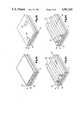
- FIGS. 1a through 1hare perspective sectional views somewhat diagrammatic showing various steps in one method of producing a structure according to this invention.
- FIGS. 2a through 2mare perspective sectional views somewhat diagrammatic showing various steps in another method of producing a structure according to this invention.
- FIGS. 1a through 1fthe various steps in producing a structure according to one method of the present invention are depicted, somewhat diagrammatically.
- insulating substrate material 10such as SiO 2 is provided which may overlie the devices on a VLSI or ULSI integrated circuit chip (not shown).
- the insulating material 10has disposed thereon metal lines 12 which may be aluminum or other metal which have been patterned by conventional photolithographic techniques to provide the desired wiring structure on top of the insulating layer 10.
- a layer of removable material 14is deposited atop the substrate material 10 and around the metal lines 12.
- the preferred material for thisis a poly-para-xylylene, (PPX) an organic polymer sold by Union Carbid Corporation, under the Trademark Parylene N, which can be readily selectively removed under certain specific conditions as will be described presently.
- PPXpoly-para-xylylene
- other removable materialswhich have the property of being etched or consumed at a rate significantly and substantially faster than any of the material surrounding it (i.e. the metal and silicon dioxide) can also be used.
- Other such additional materialsinclude spun on glasses which can be removed in HF acid etch.
- parylenewhen used, this can be deposited by chemical vapor deposition (CVD) techniques which are well known in the art.
- CVD deposition by the Gorham methodis a very good technique. This is done after first optionally applying an adhesion promoter such as A1100 sold by Shipley Co. Thereafter the PPX is applied by heating the PPX source material to 165° C. and passing the vapor through a furnace in a tube at 425° C. and thereafter depositing the heated vapor onto the substrate in a chamber at 40 microns pressure and room temperature.
- CVD deposition by the Gorham methodis a very good technique. This is done after first optionally applying an adhesion promoter such as A1100 sold by Shipley Co. Thereafter the PPX is applied by heating the PPX source material to 165° C. and passing the vapor through a furnace in a tube at 425° C. and thereafter depositing the heated vapor onto the substrate in a chamber at 40 microns pressure and room temperature.
- the materialWhen the
- etch back techniqueis as follows: A layer of planarizing resist material, such as AZ1350 sold by Shipley Co. is spun applied and then baked at about 120° C. This is followed by etching in O 2 in a reactive ion etching tool. This etching continues until all the resist has been removed and the resulting structure is a planarized surface of parylene 14 and metal lines 12. This structure is shown in FIG. 1b.
- a layer of planarizing resist materialsuch as AZ1350 sold by Shipley Co. is spun applied and then baked at about 120° C. This is followed by etching in O 2 in a reactive ion etching tool. This etching continues until all the resist has been removed and the resulting structure is a planarized surface of parylene 14 and metal lines 12. This structure is shown in FIG. 1b.
- An insulating cap material 16is then deposited on top of the planarized parylene surface and metal, which cap preferably also is silicon dioxide which can be deposited by conventional techniques.
- the SiO 2is deposited in an AME 3300 deposition tool using 1.9% SiH 4 with He at 3000 sccm, and N 2 O at 2500 sccm, carried out at a pressure of 2.0 Torr, a temperature of 340° C., and a power of 150 watts.
- a layer of photoresist material 18is deposited on top of the insulating material 16 and patterned by conventional photolithographic processes so as to provide the desired opening configurations 19 for access to the metal lines and to parylene material as will become clear presently and as shown in FIG. 1c.
- the revealed SiO 2 material on the cap 16 underlying the openings 19is removed by any conventional etching technique utilizing the unexposed remaining photoresist material 18 as a mask.
- One such techniquebeing as follows: The SiO 2 is etched in an AME 8100 etching tool using CHF 3 at 75 sccm, and CO 2 at 8 sccm, carried out at 40 millitor, at ambient temperature and at a power of 1200 watts. The remaining photoresist 18 is then removed. This will result in the structure shown in FIG. 1d. As can be seen in FIG.
- openings 20there are a plurality of openings one of which is shown at 20, which extends through the cap material 16 to the underlying metalization layer 12, while other openings, one of which is shown at 22, extend through the insulating cap material 16 and communicate with the underlying parylene material 14.
- the openings 20will be used to provide interlayer contact and the openings 22 will be used as access openings to remove the material 14 as will be described presently.
- a metal such as tungsten 24is deposited in the openings 20 as shown in FIG. 1e which can be effectively accomplished by selective deposition as follows:
- the tungstenis deposited in a Varian 5100 tool, using WF 6 at 10 sccm, H 2 at 200 sccm, SiH 4 at 10 sccm and at a temperature of about 300° C.
- the parylene materialis removed through the access openings by heating the entire structure in the O 2 rich atmosphere at a temperature of about 200° C. This will cause the parylene material 14 to react with the oxygen in the atmosphere and essentially turn to gas and be expelled through the access openings 22 leaving spaces 25 between the metal lines 12 and between the base layer 10 and the cap 16 as shown in FIG. 1f.
- the access openings 22are filled, preferably by a technique of CVD deposition of SiO 2 utilizing an inert carrier gas at a pressure of about 100 millitorr.
- Thisis quite a low pressure and any ambient atmosphere which is contained within the spaces between the base 10 and cap 16 and between metal lines 12 is replaced by the vacuum and a certain small amount of whatever carrier gas is used to perform chemical vapor deposition of the SiO 2 .
- This chemical deposition of SiO 2will effectively close the access openings 22, and, since the process is being carried out at the very low pressure of 100 millitorr with inert carrier gas the resulting space between the metal lines 14 has a very low pressure therein containing only small amounts of inert gas. This will give a dielectric constant of 2.0 or less.
- the SiO 2 on the cap 16 to close the acces openings 22there will also be a layer 26 of the SiO 2 material deposited on the top thereof as shown in FIG. 1g.
- This layer 26is then blanket etched by the reactive ion etching (R.I.E.) process as described above to expose the top of the tungsten as shown in FIG. 1h, which can then act as a via or stud for interlayer connection.
- the desired metallizationcan then be applied to the top of the cap layer 16, and the whole process repeated if additional layers of metallizations are desired.
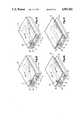
- FIGS. 2a through 2mthe steps in another embodiment of this invention are shown which is particularly effective for providing not only intralayer insulation between two metal lines on a given layer, but also is especially effective for providing interlayer insulation of metal lines on two superposed layers of insulation.
- a first layer of metal 31such as tungsten is blanket deposited onto an insulating substrate 30 such as silicon dioxide by any suitable deposition technique.
- a sputter processutilizing a Perkins-Elmer 4450 tool at 600 watts D.C. magnetron sputtering at 10-30 millitorr pressure with a bias of between 0 and-60 volts.
- a layer of aluminumis blanket deposited onto the tungsten by any suitable process. This aluminum can be deposited by using an RF evaporation source at a pressure of about 1 microtorr.
- a silicon dioxide layer 34is deposited as previously described.
- silicon dioxide layer 34On top of the silicon dioxide layer 34 a layer of silicon nitride 36 is deposited.
- the silicon nitride depositionis preferably done in an ASM tool utilizing SiH 4 at 175 sccm, and NH 3 at 325 sccm, carried out at a pressure of 2 torr, a temperature of 375° C., and a power of 160 watts. This is the starting structure and is shown in FIG. 2a.
- the overlying silicon nitride layer 36is then patterned by convention photolithographic techniques and reactive ion etched to provide the structure shown in FIG. 2b wherein there are a series of pads of silicon nitride 36 atop the silicon dioxide layer 34.
- a layer of photoresist material 38is then deposited over the surface of the structure shown in FIG. 2b and patterned and developed in a conventional manner to provide the pattern shown in FIG. 2c.
- the pattern of the photoresist 38corresponds to the desired pattern of lines which will be etched in the underlying metal layer 32 as will become apparent presently.
- the silicon nitride pads 36have been intentionally made slightly wider than the width of the photoresist pattern material 38 so as to provide a self-aligning feature which is well known in the art. At this point the excess nitride 36 is trimmed in an AME Hexode tool using CHF 3 at 75 sccm, and O 2 at 10 sccm, carried out at a power of 800 watts. This provides the structure shown in FIG. 2d.
- the structureis etched using the undeveloped photoresist pattern 38 as a mask, the etching first being through the exposed silicon dioxide 34 down to the exposed metal layer 32 and thereafter the aluminum metal layer 32 is etched so as to reveal the underlying tungsten 31 and provide a line pattern as shown in FIG. 2e.
- This etchingtakes place by the following process: First the SIO 2 is etched as previously described until it is completely removed to expose the aluminum metal.
- the aluminumis etched in an AME 8300 tool using a multi-step process as follows:
- BCl 3at 140 sccm, Cl 2 , at 30 sccm, CH 3 at 15 sccm, and CH 4 at 15 sccm, carried out at a pressure of 30 millitorr and a D.C. bias of -160 volts until the unmasked aluminum is removed.
- the silicon dioxide which underlies the photoresist but which is not covered by the Si 3 N 4 pads 36is removed by etching as previously described, the pads 36 acting as etch marks on the SiO 2 layer 34 and the tungsten 31 acting as an etch mask on the SiO 2 layer 30.
- the tungsten 31is then removed by any suitable means, such as by reactive ion etching in a suitable gas such as SF 6 at a rate of 150 nm per minute. This will provide the structure as shown in FIG. 2f.
- underlying aluminum metal lines 32have disposed thereon stanchions 40, two of which are shown in FIG. 2f, each stanchions being comprised of a silicon nitride layer 36 and a silicon dioxide layer 34.
- Removable material 41such as parylene is deposited(as previously described) onto the surface of the substrate 30 so that it fills between the metal lines 32 and around the stanchions 40, and is planarized back as previously described to the structure shown in FIG. 2g. (The silicon nitride need not remain after this point in the process, and if desired can be removed as a part of the planarization operation using conventional techniques as previously described.)
- a cap layer 42 of silicon dioxideis then blanket deposited on top of the structure shown in FIG. 2h.
- a layer of photo resistis deposited on the cap layer 42 and patterned and developed as described in the previous embodiment to provide for the necessary via and access openings.
- Via openings, one of which is shown at 44, and access opeinings 46,are etched through the silicon dioxide cap layer 42 by the technique as previously described, the via openings being located above the stanchions 40 and the removal or access openings 46 being located above the removable material 41 and the photoresist material removed to provide the structure as shown in FIG. 2i. It should be noted that the etching of the via hole 44 proceeds through both the oxide cap material 42 and the silicon nitride 36 and the underlying oxide material 34 to the metal 32.
- This etching processis carried out in an AME 8100 etching tool wherein the SiO 2 is first etched as previously described to remove the SiO 2 revealing the silicon nitride. The silicon nitride is then etched in an AME Hexode tool as previously described to reveal the SiO 2 . This final layer of SiO 2 is etched as previously described to reveal the underlying aluminum lines.
- metal 48is deposited into the via 44 to provide an interconnection which preferably is tungsten as previously described and shown in FIG. 2j.
- the material 41is then removed as previously described. It the material is parylene it is removed by heating the structure in an O 2 atmosphere at about 200° C. or less until the material is removed as shown in FIG. 2k providing spaces 50 between the lines 32 and between the base 30 and cap 42. If the material is spun on glass it can be etched out by a solution of 100 parts HNO 3 , 100 parts H 2 O, and 1 part HF. If other material is used it can be suitable removed by selecting enchants that do not significantly react either with the silicon dioxide, or the silicon nitride or the metal.
- the structureis then subjected to a CVD silicon dioxide deposition as previously described to close the access openings 46 and provide a layer 52 on top of cap 42 which when done at a pressure of 100 millitorr will result in a relatively low pressure spaces 50 as shown in FIG. 2l.
- the layer 52is then etched back as previously described to provide the resulting structure shown in FIG. 2m.
- This particular embodimentis particularly adapted not only for use with intralayer insulation but also interlayer insulation in that there is provided a plurality of stanchions or supports 40 separating the base layer 30 and cap layer 42, which stanchions are comprised of a layer of silicon dioxide and silicon nitride overlying the metal lines 32 thus increasing the space 50 constituting the space between the layer 32 and the cap 42.
Landscapes
- Engineering & Computer Science (AREA)
- Physics & Mathematics (AREA)
- Condensed Matter Physics & Semiconductors (AREA)
- General Physics & Mathematics (AREA)
- Computer Hardware Design (AREA)
- Microelectronics & Electronic Packaging (AREA)
- Power Engineering (AREA)
- Manufacturing & Machinery (AREA)
- Internal Circuitry In Semiconductor Integrated Circuit Devices (AREA)
- Electrodes Of Semiconductors (AREA)
Abstract
Description
This invention relates generally to a method and structure for reducing the capacitive coupling either between lines on the same layer (intralayer) or between lines on superposed layers (interlayer) in VLSI or ULSI circuits. In more particular aspects the present invention relates to a method and structure for yielding an effectively reduced dielectric constant between lines on the surface of a given VLSI or ULSI chip or on lines mounted on various layers or surfaces on VLSI or ULSI structures utilizing air, other gasses, or a partial vacuum as a dielectric medium.
It has been conventional prior art practice in integrated circuit chip production to utilize materials such as silicon dioxide, silicon nitride, polyimides and certain other organic materials as delectric materials interposed between the metal lines on a give layer and between various layers of metalization in the wiring portion of the integrated circuit chip.
However, as the integrated circuit technology progresses into a Very Large Scale Intergration (VLSI) and beyond to Ultra Large Scale Integration (ULSI) the spacing between the metal lines on any given plane and the interplanar spacing of metal lines becomes less and less, extending into the submicron range for intralayer spacing. This increases the capacitive losses between the lines and gives rise to a need for the space between the lines having improved dielectric properties; i.e., with a dielectric constant as low as possible.
The dielectric constants of silicon nitride (which is about 7.0), CVD silicon dioxide (which is 3.9), and polyimides (which are about 3.6), are not sufficiently low to provide acceptable insulation in these submicron ranges; hence, it is necessary to provide a medium with improved dielectric properties, e.g. a constant of 2.0 or less in the intraplanar spaces between lines and interplanar spaces between lines at different levels.
According to the present invention a method and structure for providing an insulating electrical space between two lines on a layer of material or between lines on adjacent superposed layers of material are provided. According to this invention a base member is formed having a plurality of support members extending upwardly from said base member. A removable material is deposited on said base member and around said support members. A cap member of insulating material is then disposed over said support members and said removable material. Access openings are formed in at least one of the base member or the cap member communicating with said removable material. The removable material is removed through the access openings to thereby define a space between said cap member and said base member and between said support members. During this step a partial vacuum (in which some inert gas may be dispersed) may be created in the space vacated by the removable material. The access openings are then filled in so as to provide a sealed space between the cap member and the base member which has a very low dielectric constant.
FIGS. 1a through 1h are perspective sectional views somewhat diagrammatic showing various steps in one method of producing a structure according to this invention; and
FIGS. 2a through 2m are perspective sectional views somewhat diagrammatic showing various steps in another method of producing a structure according to this invention.
Referring now to the drawing and for the present FIGS. 1a through 1f the various steps in producing a structure according to one method of the present invention are depicted, somewhat diagrammatically. As shown in FIG. 1a insulatingsubstrate material 10 such as SiO2 is provided which may overlie the devices on a VLSI or ULSI integrated circuit chip (not shown). The insulatingmaterial 10 has disposed thereonmetal lines 12 which may be aluminum or other metal which have been patterned by conventional photolithographic techniques to provide the desired wiring structure on top of the insulatinglayer 10. A layer ofremovable material 14 is deposited atop thesubstrate material 10 and around the metal lines 12. The preferred material for this is a poly-para-xylylene, (PPX) an organic polymer sold by Union Carbid Corporation, under the Trademark Parylene N, which can be readily selectively removed under certain specific conditions as will be described presently. However, other removable materials which have the property of being etched or consumed at a rate significantly and substantially faster than any of the material surrounding it (i.e. the metal and silicon dioxide) can also be used. Other such additional materials include spun on glasses which can be removed in HF acid etch.
When parylene is used, this can be deposited by chemical vapor deposition (CVD) techniques which are well known in the art. For example, CVD deposition by the Gorham method is a very good technique. This is done after first optionally applying an adhesion promoter such as A1100 sold by Shipley Co. Thereafter the PPX is applied by heating the PPX source material to 165° C. and passing the vapor through a furnace in a tube at 425° C. and thereafter depositing the heated vapor onto the substrate in a chamber at 40 microns pressure and room temperature. When the material has been deposited it is planarized by a suitable technique such as an etch back or other planarization techniques so that the top surface is flush with the top of themetal lines 12. One such etch back technique is as follows: A layer of planarizing resist material, such as AZ1350 sold by Shipley Co. is spun applied and then baked at about 120° C. This is followed by etching in O2 in a reactive ion etching tool. This etching continues until all the resist has been removed and the resulting structure is a planarized surface ofparylene 14 andmetal lines 12. This structure is shown in FIG. 1b.
Aninsulating cap material 16 is then deposited on top of the planarized parylene surface and metal, which cap preferably also is silicon dioxide which can be deposited by conventional techniques. In one such technique the SiO2 is deposited in an AME 3300 deposition tool using 1.9% SiH4 with He at 3000 sccm, and N2 O at 2500 sccm, carried out at a pressure of 2.0 Torr, a temperature of 340° C., and a power of 150 watts. Following this, a layer ofphotoresist material 18 is deposited on top of theinsulating material 16 and patterned by conventional photolithographic processes so as to provide the desiredopening configurations 19 for access to the metal lines and to parylene material as will become clear presently and as shown in FIG. 1c.
The revealed SiO2 material on thecap 16 underlying theopenings 19 is removed by any conventional etching technique utilizing the unexposed remainingphotoresist material 18 as a mask. One such technique being as follows: The SiO2 is etched in an AME 8100 etching tool using CHF3 at 75 sccm, and CO2 at 8 sccm, carried out at 40 millitor, at ambient temperature and at a power of 1200 watts. Theremaining photoresist 18 is then removed. This will result in the structure shown in FIG. 1d. As can be seen in FIG. 1d there are a plurality of openings one of which is shown at 20, which extends through thecap material 16 to theunderlying metalization layer 12, while other openings, one of which is shown at 22, extend through theinsulating cap material 16 and communicate with theunderlying parylene material 14. Theopenings 20 will be used to provide interlayer contact and theopenings 22 will be used as access openings to remove thematerial 14 as will be described presently.
A metal such astungsten 24 is deposited in theopenings 20 as shown in FIG. 1e which can be effectively accomplished by selective deposition as follows: The tungsten is deposited in a Varian 5100 tool, using WF6 at 10 sccm, H2 at 200 sccm, SiH4 at 10 sccm and at a temperature of about 300° C.
Following the tungsten deposition, the parylene material is removed through the access openings by heating the entire structure in the O2 rich atmosphere at a temperature of about 200° C. This will cause theparylene material 14 to react with the oxygen in the atmosphere and essentially turn to gas and be expelled through theaccess openings 22 leavingspaces 25 between themetal lines 12 and between thebase layer 10 and thecap 16 as shown in FIG. 1f.
At this point in the process, theaccess openings 22 are filled, preferably by a technique of CVD deposition of SiO2 utilizing an inert carrier gas at a pressure of about 100 millitorr. This is quite a low pressure and any ambient atmosphere which is contained within the spaces between thebase 10 andcap 16 and betweenmetal lines 12 is replaced by the vacuum and a certain small amount of whatever carrier gas is used to perform chemical vapor deposition of the SiO2. This chemical deposition of SiO2 will effectively close theaccess openings 22, and, since the process is being carried out at the very low pressure of 100 millitorr with inert carrier gas the resulting space between themetal lines 14 has a very low pressure therein containing only small amounts of inert gas. This will give a dielectric constant of 2.0 or less.
In the deposition of the SiO2 on thecap 16 to close theacces openings 22 there will also be alayer 26 of the SiO2 material deposited on the top thereof as shown in FIG. 1g. Thislayer 26 is then blanket etched by the reactive ion etching (R.I.E.) process as described above to expose the top of the tungsten as shown in FIG. 1h, which can then act as a via or stud for interlayer connection. The desired metallization can then be applied to the top of thecap layer 16, and the whole process repeated if additional layers of metallizations are desired.
Referring, now to FIGS. 2a through 2m the steps in another embodiment of this invention are shown which is particularly effective for providing not only intralayer insulation between two metal lines on a given layer, but also is especially effective for providing interlayer insulation of metal lines on two superposed layers of insulation.
In this embodiment, a first layer ofmetal 31 such as tungsten is blanket deposited onto an insulatingsubstrate 30 such as silicon dioxide by any suitable deposition technique. One such technique is a sputter process utilizing a Perkins-Elmer 4450 tool at 600 watts D.C. magnetron sputtering at 10-30 millitorr pressure with a bias of between 0 and-60 volts. Thereafter a layer of aluminum is blanket deposited onto the tungsten by any suitable process. This aluminum can be deposited by using an RF evaporation source at a pressure of about 1 microtorr. On top of thealuminum metal 32, asilicon dioxide layer 34 is deposited as previously described. On top of the silicon dioxide layer 34 a layer ofsilicon nitride 36 is deposited. The silicon nitride deposition is preferably done in an ASM tool utilizing SiH4 at 175 sccm, and NH3 at 325 sccm, carried out at a pressure of 2 torr, a temperature of 375° C., and a power of 160 watts. This is the starting structure and is shown in FIG. 2a.
The overlyingsilicon nitride layer 36 is then patterned by convention photolithographic techniques and reactive ion etched to provide the structure shown in FIG. 2b wherein there are a series of pads ofsilicon nitride 36 atop thesilicon dioxide layer 34.
A layer ofphotoresist material 38 is then deposited over the surface of the structure shown in FIG. 2b and patterned and developed in a conventional manner to provide the pattern shown in FIG. 2c. The pattern of thephotoresist 38 corresponds to the desired pattern of lines which will be etched in theunderlying metal layer 32 as will become apparent presently.
Thesilicon nitride pads 36 have been intentionally made slightly wider than the width of thephotoresist pattern material 38 so as to provide a self-aligning feature which is well known in the art. At this point theexcess nitride 36 is trimmed in an AME Hexode tool using CHF3 at 75 sccm, and O2 at 10 sccm, carried out at a power of 800 watts. This provides the structure shown in FIG. 2d.
At this point the structure is etched using theundeveloped photoresist pattern 38 as a mask, the etching first being through the exposedsilicon dioxide 34 down to the exposedmetal layer 32 and thereafter thealuminum metal layer 32 is etched so as to reveal the underlyingtungsten 31 and provide a line pattern as shown in FIG. 2e. This etching takes place by the following process: First the SIO2 is etched as previously described until it is completely removed to expose the aluminum metal. The aluminum is etched in an AME 8300 tool using a multi-step process as follows:
first in CF4 at 40 sccm, carried out at a pressure of 25 millitorr with a D.C. bias of 25 volts;
thereafter in BCl3 at 140 sccm, Cl2, at 30 sccm, CH3 at 15 sccm, and CH4 at 15 sccm, carried out at a pressure of 30 millitorr and a D.C. bias of -160 volts until the unmasked aluminum is removed.
At this point the remainingphotoresist 38 is stripped away. The silicon dioxide which underlies the photoresist but which is not covered by the Si3 N4 pads 36 is removed by etching as previously described, thepads 36 acting as etch marks on the SiO2 layer 34 and thetungsten 31 acting as an etch mask on the SiO2 layer 30. Thetungsten 31 is then removed by any suitable means, such as by reactive ion etching in a suitable gas such as SF6 at a rate of 150 nm per minute. This will provide the structure as shown in FIG. 2f. At this stage in the process underlyingaluminum metal lines 32 have disposed thereonstanchions 40, two of which are shown in FIG. 2f, each stanchions being comprised of asilicon nitride layer 36 and asilicon dioxide layer 34.
Acap layer 42 of silicon dioxide is then blanket deposited on top of the structure shown in FIG. 2h. A layer of photo resist is deposited on thecap layer 42 and patterned and developed as described in the previous embodiment to provide for the necessary via and access openings. Via openings, one of which is shown at 44, and accessopeinings 46, are etched through the silicondioxide cap layer 42 by the technique as previously described, the via openings being located above thestanchions 40 and the removal oraccess openings 46 being located above theremovable material 41 and the photoresist material removed to provide the structure as shown in FIG. 2i. It should be noted that the etching of the viahole 44 proceeds through both theoxide cap material 42 and thesilicon nitride 36 and theunderlying oxide material 34 to themetal 32. This etching process is carried out in an AME 8100 etching tool wherein the SiO2 is first etched as previously described to remove the SiO2 revealing the silicon nitride. The silicon nitride is then etched in an AME Hexode tool as previously described to reveal the SiO2. This final layer of SiO2 is etched as previously described to reveal the underlying aluminum lines.
As in the previously described embodiment,metal 48 is deposited into the via 44 to provide an interconnection which preferably is tungsten as previously described and shown in FIG. 2j. Thematerial 41 is then removed as previously described. It the material is parylene it is removed by heating the structure in an O2 atmosphere at about 200° C. or less until the material is removed as shown in FIG.2k providing spaces 50 between thelines 32 and between the base 30 andcap 42. If the material is spun on glass it can be etched out by a solution of 100 parts HNO3, 100 parts H2 O, and 1 part HF. If other material is used it can be suitable removed by selecting enchants that do not significantly react either with the silicon dioxide, or the silicon nitride or the metal.
The structure is then subjected to a CVD silicon dioxide deposition as previously described to close theaccess openings 46 and provide a layer 52 on top ofcap 42 which when done at a pressure of 100 millitorr will result in a relativelylow pressure spaces 50 as shown in FIG. 2l. The layer 52 is then etched back as previously described to provide the resulting structure shown in FIG. 2m.
This particular embodiment is particularly adapted not only for use with intralayer insulation but also interlayer insulation in that there is provided a plurality of stanchions or supports 40 separating thebase layer 30 andcap layer 42, which stanchions are comprised of a layer of silicon dioxide and silicon nitride overlying themetal lines 32 thus increasing thespace 50 constituting the space between thelayer 32 and thecap 42.
While several embodiments of this invention have been shown and described, various adaptations and modifications can be made without departing from the scope of the invention as defined in the appended claims.
Claims (11)
1. A method of providing an electrically insulating medium between a pair of superposed members comprising the steps of;
providing a base member of insulating material;
forming a plurality of discrete spaced support means extending upwardly from said base member;
depositing a selectively removable material on said base member around said support means;
providing a cap member of insulating material overlying said support means and said removable material;
forming access opening means in at least one of said cap or said base members communicating with said removable material;
removing said removable material through said access opening means without appreciably removing any of the base member or the cap member or the support means to thereby define a space between said base member and said cap member and around said support means and thereafter sealing said openings with insulating material;
thereby providing a space between said members and around said support means of a low dielectric constant.
2. The invention as defined in claim 1 wherein said support means includes a plurality of metal lines formed on said base member.
3. The invention as defined in claim 2 wherein said cap member is deposited directly onto said metal lines and said removable material.
4. The invention as defined in claim 1 wherein said support means include a plurality of stanchions formed by the insulating material.
5. The invention as defined in claim 1 further characterized by providing via openings through said insulating cap member, and filling said openings with a metal.
6. The invention as defined in claim 4 wherein said stanchions are formed by deposition and selective etching of insulating materials.
7. The invention as defined in claim 1 wherein said base member is silicon dioxide and said cap member is silicon dioxide.
8. The invention as defined in claim 1 wherein a vacuum is created in said space during the step of depositing the insulating material in said access openings.
9. The invention as defined in claim 1 wherein said removable material is poly-para-xylylene.
10. The invention as defined in claim 1 wherein said removable material is spun on glass.
11. The invention as defined in claim 1 wherein the dielectric constant in said space is less than 2.0.
Priority Applications (5)
| Application Number | Priority Date | Filing Date | Title |
|---|---|---|---|
| US07/286,443US4987101A (en) | 1988-12-16 | 1988-12-16 | Method for providing improved insulation in VLSI and ULSI circuits |
| DE68924468TDE68924468T2 (en) | 1988-12-16 | 1989-11-08 | Method and structure for producing insulation from VLSI and ULSI circuits. |
| EP89120666AEP0373360B1 (en) | 1988-12-16 | 1989-11-08 | Method and structure for providing improved insulation in VLSI and ULSI circuits |
| JP1324166AJPH0685415B2 (en) | 1988-12-16 | 1989-12-15 | Method for providing an electrically insulating medium between a pair of overlapping members and structure provided |
| US07/590,290US5144411A (en) | 1988-12-16 | 1990-09-28 | Method and structure for providing improved insulation in vlsi and ulsi circuits |
Applications Claiming Priority (1)
| Application Number | Priority Date | Filing Date | Title |
|---|---|---|---|
| US07/286,443US4987101A (en) | 1988-12-16 | 1988-12-16 | Method for providing improved insulation in VLSI and ULSI circuits |
Related Child Applications (1)
| Application Number | Title | Priority Date | Filing Date |
|---|---|---|---|
| US07/590,290DivisionUS5144411A (en) | 1988-12-16 | 1990-09-28 | Method and structure for providing improved insulation in vlsi and ulsi circuits |
Publications (1)
| Publication Number | Publication Date |
|---|---|
| US4987101Atrue US4987101A (en) | 1991-01-22 |
Family
ID=23098630
Family Applications (2)
| Application Number | Title | Priority Date | Filing Date |
|---|---|---|---|
| US07/286,443Expired - Fee RelatedUS4987101A (en) | 1988-12-16 | 1988-12-16 | Method for providing improved insulation in VLSI and ULSI circuits |
| US07/590,290Expired - LifetimeUS5144411A (en) | 1988-12-16 | 1990-09-28 | Method and structure for providing improved insulation in vlsi and ulsi circuits |
Family Applications After (1)
| Application Number | Title | Priority Date | Filing Date |
|---|---|---|---|
| US07/590,290Expired - LifetimeUS5144411A (en) | 1988-12-16 | 1990-09-28 | Method and structure for providing improved insulation in vlsi and ulsi circuits |
Country Status (4)
| Country | Link |
|---|---|
| US (2) | US4987101A (en) |
| EP (1) | EP0373360B1 (en) |
| JP (1) | JPH0685415B2 (en) |
| DE (1) | DE68924468T2 (en) |
Cited By (67)
| Publication number | Priority date | Publication date | Assignee | Title |
|---|---|---|---|---|
| US5308440A (en)* | 1991-09-05 | 1994-05-03 | Matsushita Electric Industrial Co., Ltd. | Method of making semiconductor device with air-bridge interconnection |
| US5407860A (en)* | 1994-05-27 | 1995-04-18 | Texas Instruments Incorporated | Method of forming air gap dielectric spaces between semiconductor leads |
| US5422590A (en)* | 1993-01-05 | 1995-06-06 | Texas Instruments Incorporated | High voltage negative charge pump with low voltage CMOS transistors |
| US5432128A (en)* | 1994-05-27 | 1995-07-11 | Texas Instruments Incorporated | Reliability enhancement of aluminum interconnects by reacting aluminum leads with a strengthening gas |
| US5461003A (en)* | 1994-05-27 | 1995-10-24 | Texas Instruments Incorporated | Multilevel interconnect structure with air gaps formed between metal leads |
| US5470802A (en)* | 1994-05-20 | 1995-11-28 | Texas Instruments Incorporated | Method of making a semiconductor device using a low dielectric constant material |
| US5472913A (en)* | 1994-08-05 | 1995-12-05 | Texas Instruments Incorporated | Method of fabricating porous dielectric material with a passivation layer for electronics applications |
| EP0687004A1 (en) | 1994-06-07 | 1995-12-13 | Texas Instruments Incorporated | Method for fabrication of dielectrics on semiconductor devices |
| US5476817A (en)* | 1994-05-31 | 1995-12-19 | Texas Instruments Incorporated | Method of making reliable metal leads in high speed LSI semiconductors using both dummy leads and thermoconductive layers |
| EP0688052A2 (en) | 1994-05-20 | 1995-12-20 | Texas Instruments Incorporated | Improvements in or relating to fabrication of semiconductor devices |
| EP0692824A2 (en) | 1994-07-15 | 1996-01-17 | Texas Instruments Incorporated | Improvements in and relating to semiconductor devices |
| US5510293A (en)* | 1994-05-31 | 1996-04-23 | Texas Instruments Incorporated | Method of making reliable metal leads in high speed LSI semiconductors using thermoconductive layers |
| US5512775A (en)* | 1994-04-28 | 1996-04-30 | Texas Instruments Incorporated | Low dielectric constant insulation in VLSI applications |
| US5523615A (en)* | 1994-06-23 | 1996-06-04 | Texas Instruments Incorporated | Porous dielectric material with improved pore surface properties for electronics applications |
| US5525857A (en)* | 1994-08-19 | 1996-06-11 | Texas Instruments Inc. | Low density, high porosity material as gate dielectric for field emission device |
| US5670828A (en)* | 1995-02-21 | 1997-09-23 | Advanced Micro Devices, Inc. | Tunneling technology for reducing intra-conductive layer capacitance |
| US5728628A (en)* | 1994-05-27 | 1998-03-17 | Texas Instruments Incorporated | Two-step metal etch process for selective gap fill of submicron inter-connects and structure for same |
| US5751056A (en)* | 1994-05-31 | 1998-05-12 | Texas Instruments Incorporated | Reliable metal leads in high speed LSI semiconductors using dummy leads |
| US5801092A (en)* | 1997-09-04 | 1998-09-01 | Ayers; Michael R. | Method of making two-component nanospheres and their use as a low dielectric constant material for semiconductor devices |
| US5818110A (en)* | 1996-11-22 | 1998-10-06 | International Business Machines Corporation | Integrated circuit chip wiring structure with crossover capability and method of manufacturing the same |
| US5847439A (en)* | 1995-06-07 | 1998-12-08 | Micron Technology, Inc. | Integrated circuit having a void between adjacent conductive lines |
| US5861653A (en)* | 1995-05-11 | 1999-01-19 | Nec Corporation | Semiconductor device having gaseous isolating layer formed in inter-level insulating layer and process of fabrication thereof |
| US5880018A (en)* | 1996-10-07 | 1999-03-09 | Motorola Inc. | Method for manufacturing a low dielectric constant inter-level integrated circuit structure |
| US5882963A (en)* | 1994-11-24 | 1999-03-16 | Siemens Aktiengesellschaft | Method of manufacturing semiconductor components |
| US5908318A (en)* | 1995-12-08 | 1999-06-01 | Advanced Micro Devices, Inc. | Method of forming low capacitance interconnect structures on semiconductor substrates |
| US5965465A (en)* | 1997-09-18 | 1999-10-12 | International Business Machines Corporation | Etching of silicon nitride |
| US6033996A (en)* | 1997-11-13 | 2000-03-07 | International Business Machines Corporation | Process for removing etching residues, etching mask and silicon nitride and/or silicon dioxide |
| US6090724A (en)* | 1998-12-15 | 2000-07-18 | Lsi Logic Corporation | Method for composing a thermally conductive thin film having a low dielectric property |
| US6117796A (en)* | 1998-08-13 | 2000-09-12 | International Business Machines Corporation | Removal of silicon oxide |
| WO2000054312A1 (en)* | 1999-03-12 | 2000-09-14 | California Institute Of Technology | Ic-compatible parylene mems technology and its application in integrated sensors |
| US6150282A (en)* | 1997-11-13 | 2000-11-21 | International Business Machines Corporation | Selective removal of etching residues |
| US6162838A (en)* | 1998-06-05 | 2000-12-19 | Georgia Tech Research Corporation | Porous insulating compounds and method for making same |
| US6165890A (en)* | 1997-01-21 | 2000-12-26 | Georgia Tech Research Corporation | Fabrication of a semiconductor device with air gaps for ultra-low capacitance interconnections |
| US6200891B1 (en) | 1998-08-13 | 2001-03-13 | International Business Machines Corporation | Removal of dielectric oxides |
| US6277766B1 (en) | 2000-02-03 | 2001-08-21 | Michael Raymond Ayers | Method of making fullerene-decorated nanoparticles and their use as a low dielectric constant material for semiconductor devices |
| US6307265B1 (en)* | 1995-12-28 | 2001-10-23 | Kabushiki Kaisha Toshiba | Feasible, gas-dielectric interconnect process |
| US20010041459A1 (en)* | 1995-11-16 | 2001-11-15 | Smith Douglas M. | Polyol-based method for forming thin film aerogels on semiconductor substrates |
| US6319858B1 (en)* | 2000-07-11 | 2001-11-20 | Nano-Architect Research Corporation | Methods for reducing a dielectric constant of a dielectric film and for forming a low dielectric constant porous film |
| US6319852B1 (en) | 1995-11-16 | 2001-11-20 | Texas Instruments Incorporated | Nanoporous dielectric thin film formation using a post-deposition catalyst |
| US6329062B1 (en) | 2000-02-29 | 2001-12-11 | Novellus Systems, Inc. | Dielectric layer including silicalite crystals and binder and method for producing same for microelectronic circuits |
| US6380105B1 (en) | 1996-11-14 | 2002-04-30 | Texas Instruments Incorporated | Low volatility solvent-based method for forming thin film nanoporous aerogels on semiconductor substrates |
| US6437007B1 (en) | 1995-11-16 | 2002-08-20 | Texas Instruments Incorporated | Aerogel thin film formation from multi-solvent systems |
| US20020140007A1 (en)* | 2001-03-30 | 2002-10-03 | Fujitsu Quantum Devices Limited | Semiconductor device and method for fabricating the same |
| US6498031B1 (en) | 1999-05-28 | 2002-12-24 | Oxidor Corporation, Inc. | Column reactor for testing and evaluating refractory ores |
| US6576976B2 (en) | 1997-01-03 | 2003-06-10 | Integrated Device Technology, Inc. | Semiconductor integrated circuit with an insulation structure having reduced permittivity |
| US6576848B1 (en) | 1996-11-22 | 2003-06-10 | International Business Machines Corporation | Integrated circuit chip wiring structure with crossover capability and method of manufacturing the same |
| US6610593B2 (en) | 2000-08-31 | 2003-08-26 | Georgia Tech Research Corporation | Fabrication of semiconductor device with air gaps for ultra low capacitance interconnections and methods of making same |
| US6614097B1 (en) | 1998-09-30 | 2003-09-02 | Lsi Logic Corporation | Method for composing a dielectric layer within an interconnect structure of a multilayer semiconductor device |
| US6710538B1 (en) | 1998-08-26 | 2004-03-23 | Micron Technology, Inc. | Field emission display having reduced power requirements and method |
| US20040075159A1 (en)* | 2002-10-17 | 2004-04-22 | Nantero, Inc. | Nanoscopic tunnel |
| US20040077107A1 (en)* | 2002-10-17 | 2004-04-22 | Nantero, Inc. | Method of making nanoscopic tunnel |
| US20040087162A1 (en)* | 2002-10-17 | 2004-05-06 | Nantero, Inc. | Metal sacrificial layer |
| US20040137728A1 (en)* | 2002-09-13 | 2004-07-15 | Shipley Company, L.L.C. | Air gap formation |
| US20050124172A1 (en)* | 2002-04-02 | 2005-06-09 | Townsend Iii Paul H. | Process for making air gap containing semiconducting devices and resulting semiconducting device |
| US20050215047A1 (en)* | 2004-03-17 | 2005-09-29 | Roel Daamen | Method of manufacturing a semiconductor device having damascene structures with air gaps |
| US6995439B1 (en)* | 2002-06-12 | 2006-02-07 | Novellus Systems, Inc. | Method of fabricating low dielectric constant dielectric films |
| DE102005004376A1 (en)* | 2005-01-31 | 2006-08-10 | Infineon Technologies Ag | Semiconductor memory device e.g. high-density chain-ferroelectric RAM, has capacitor arrangement with capacitors serving as memory units, where memory units and capacitors are separated from each other by insulation area |
| US20060185794A1 (en)* | 2005-02-24 | 2006-08-24 | Ayers Michael Raymond | Porous films and bodies with enhanced mechanical strength |
| US20060246681A1 (en)* | 2003-02-05 | 2006-11-02 | Youngfu Li | Sacrificial benzocyclobutene/norbornene polymers for making air gap semiconductor devices |
| US20060292892A1 (en)* | 2003-02-05 | 2006-12-28 | Kirchhoff Robert A | Sacrificial benzocyclobutene copolymers for making air gap semiconductor devices |
| US20070292700A1 (en)* | 2006-05-31 | 2007-12-20 | Roskilde Semiconductor Llc | Porous materials derived from polymer composites |
| US20080020197A1 (en)* | 2006-05-31 | 2008-01-24 | Roskilde Semiconductor Llc | Porous inorganic solids for use as low dielectric constant materials |
| US20080044642A1 (en)* | 2006-05-31 | 2008-02-21 | Roskilde Semiconductor, Llc | Low dielectric constant materials prepared from soluble fullerene clusters |
| US7541277B1 (en) | 2008-04-30 | 2009-06-02 | International Business Machines Corporation | Stress relaxation, selective nitride phase removal |
| US7919188B2 (en) | 2006-05-31 | 2011-04-05 | Roskilde Semiconductor Llc | Linked periodic networks of alternating carbon and inorganic clusters for use as low dielectric constant materials |
| US20140322910A1 (en)* | 2012-05-01 | 2014-10-30 | Taiwan Semiconductor Manufacturing Company, Ltd. | Via-free interconnect structure with self-aligned metal line interconnections |
| CN109935549A (en)* | 2019-03-21 | 2019-06-25 | 长江存储科技有限责任公司 | Method of forming metal interconnection lines |
Families Citing this family (18)
| Publication number | Priority date | Publication date | Assignee | Title |
|---|---|---|---|---|
| GB2247986A (en)* | 1990-09-12 | 1992-03-18 | Marconi Gec Ltd | Reducing interconnection capacitance in integrated circuits |
| JP3074713B2 (en)* | 1990-09-18 | 2000-08-07 | 日本電気株式会社 | Method for manufacturing semiconductor device |
| GB2248072B (en)* | 1990-09-22 | 1994-03-09 | Gec Ferranti Defence Syst | A method of fabricating coaxial cable components and coaxial cable components fabricated thereby |
| US5486493A (en)* | 1994-02-25 | 1996-01-23 | Jeng; Shin-Puu | Planarized multi-level interconnect scheme with embedded low-dielectric constant insulators |
| US5759911A (en)* | 1995-08-22 | 1998-06-02 | International Business Machines Corporation | Self-aligned metallurgy |
| US6136212A (en)* | 1996-08-12 | 2000-10-24 | The Regents Of The University Of Michigan | Polymer-based micromachining for microfluidic devices |
| JP2962272B2 (en)* | 1997-04-18 | 1999-10-12 | 日本電気株式会社 | Method for manufacturing semiconductor device |
| US7211496B1 (en) | 1998-04-22 | 2007-05-01 | International Business Machines Corporation | Freestanding multiplayer IC wiring structure |
| US6097092A (en)* | 1998-04-22 | 2000-08-01 | International Business Machines Corporation | Freestanding multilayer IC wiring structure |
| US6071805A (en)* | 1999-01-25 | 2000-06-06 | Chartered Semiconductor Manufacturing, Ltd. | Air gap formation for high speed IC processing |
| DE10144847A1 (en)* | 2001-09-12 | 2003-03-27 | Infineon Technologies Ag | Production of a membrane on a semiconductor substrate comprises forming trenches in the substrate, applying a dielectric material, isotropically etching the substrate, and applying a further dielectric material |
| DE10200869A1 (en) | 2002-01-11 | 2003-07-31 | Infineon Technologies Ag | Method for producing a protective cover for a component |
| DE10316776B4 (en) | 2003-04-11 | 2005-03-17 | Infineon Technologies Ag | Method for producing a protective cover for a component |
| DE10316777B4 (en) | 2003-04-11 | 2005-11-24 | Infineon Technologies Ag | Method for producing a protective cover for a component |
| US6875685B1 (en) | 2003-10-24 | 2005-04-05 | International Business Machines Corporation | Method of forming gas dielectric with support structure |
| JP2009267347A (en)* | 2008-03-31 | 2009-11-12 | Toshiba Corp | Semiconductor device and manufacturing method thereof |
| JP4691152B2 (en) | 2008-03-31 | 2011-06-01 | 株式会社東芝 | Semiconductor device and manufacturing method thereof |
| PL2826856T3 (en) | 2013-07-16 | 2016-06-30 | Sia Latima | Genetically stable oncolytic RNA virus, method of manufacturing and use thereof |
Citations (6)
| Publication number | Priority date | Publication date | Assignee | Title |
|---|---|---|---|---|
| US3689992A (en)* | 1964-08-08 | 1972-09-12 | Telefunken Patent | Production of circuit device |
| US3890636A (en)* | 1971-09-09 | 1975-06-17 | Hitachi Ltd | Multilayer wiring structure of integrated circuit and method of producing the same |
| US3925880A (en)* | 1971-04-29 | 1975-12-16 | Signetics Corp | Semiconductor assembly with beam lead construction and method |
| US3932226A (en)* | 1974-12-06 | 1976-01-13 | Rca Corporation | Method of electrically interconnecting semiconductor elements |
| US4289846A (en)* | 1979-12-28 | 1981-09-15 | General Electric Company | Process for forming low-reactance interconnections on semiconductors |
| US4849071A (en)* | 1986-12-13 | 1989-07-18 | Spectrol Reliance Limited | Method of forming a sealed diaphragm on a substrate |
Family Cites Families (8)
| Publication number | Priority date | Publication date | Assignee | Title |
|---|---|---|---|---|
| JPS5220230B2 (en)* | 1973-06-22 | 1977-06-02 | ||
| US4379307A (en)* | 1980-06-16 | 1983-04-05 | Rockwell International Corporation | Integrated circuit chip transmission line |
| US4975762A (en)* | 1981-06-11 | 1990-12-04 | General Electric Ceramics, Inc. | Alpha-particle-emitting ceramic composite cover |
| JPS60223145A (en)* | 1984-04-20 | 1985-11-07 | Hitachi Ltd | semiconductor equipment |
| JPS62177943A (en)* | 1986-01-31 | 1987-08-04 | Nec Corp | Manufacture of multilayer interconnection structure |
| JPS62181446A (en)* | 1986-02-04 | 1987-08-08 | Mitsubishi Electric Corp | Manufacturing method of semiconductor device |
| JPS63179548A (en)* | 1987-01-21 | 1988-07-23 | Mitsubishi Electric Corp | Wiring structure of semiconductor integrated circuit device |
| JP2615608B2 (en)* | 1987-04-07 | 1997-06-04 | 日本電気株式会社 | Method for manufacturing semiconductor device |
- 1988
- 1988-12-16USUS07/286,443patent/US4987101A/ennot_activeExpired - Fee Related
- 1989
- 1989-11-08DEDE68924468Tpatent/DE68924468T2/ennot_activeExpired - Fee Related
- 1989-11-08EPEP89120666Apatent/EP0373360B1/ennot_activeExpired - Lifetime
- 1989-12-15JPJP1324166Apatent/JPH0685415B2/ennot_activeExpired - Lifetime
- 1990
- 1990-09-28USUS07/590,290patent/US5144411A/ennot_activeExpired - Lifetime
Patent Citations (6)
| Publication number | Priority date | Publication date | Assignee | Title |
|---|---|---|---|---|
| US3689992A (en)* | 1964-08-08 | 1972-09-12 | Telefunken Patent | Production of circuit device |
| US3925880A (en)* | 1971-04-29 | 1975-12-16 | Signetics Corp | Semiconductor assembly with beam lead construction and method |
| US3890636A (en)* | 1971-09-09 | 1975-06-17 | Hitachi Ltd | Multilayer wiring structure of integrated circuit and method of producing the same |
| US3932226A (en)* | 1974-12-06 | 1976-01-13 | Rca Corporation | Method of electrically interconnecting semiconductor elements |
| US4289846A (en)* | 1979-12-28 | 1981-09-15 | General Electric Company | Process for forming low-reactance interconnections on semiconductors |
| US4849071A (en)* | 1986-12-13 | 1989-07-18 | Spectrol Reliance Limited | Method of forming a sealed diaphragm on a substrate |
Cited By (118)
| Publication number | Priority date | Publication date | Assignee | Title |
|---|---|---|---|---|
| US5308440A (en)* | 1991-09-05 | 1994-05-03 | Matsushita Electric Industrial Co., Ltd. | Method of making semiconductor device with air-bridge interconnection |
| US5422590A (en)* | 1993-01-05 | 1995-06-06 | Texas Instruments Incorporated | High voltage negative charge pump with low voltage CMOS transistors |
| US5512775A (en)* | 1994-04-28 | 1996-04-30 | Texas Instruments Incorporated | Low dielectric constant insulation in VLSI applications |
| US5488015A (en)* | 1994-05-20 | 1996-01-30 | Texas Instruments Incorporated | Method of making an interconnect structure with an integrated low density dielectric |
| EP0688052A2 (en) | 1994-05-20 | 1995-12-20 | Texas Instruments Incorporated | Improvements in or relating to fabrication of semiconductor devices |
| US5470802A (en)* | 1994-05-20 | 1995-11-28 | Texas Instruments Incorporated | Method of making a semiconductor device using a low dielectric constant material |
| EP0684642A1 (en) | 1994-05-20 | 1995-11-29 | Texas Instruments Incorporated | Method of fabrication of a porous dielectric layer for a semiconductor device |
| US5747880A (en)* | 1994-05-20 | 1998-05-05 | Texas Instruments Incorporated | Interconnect structure with an integrated low density dielectric |
| US5804508A (en)* | 1994-05-20 | 1998-09-08 | Texas Instruments Incorporated | Method of making a low dielectric constant material for electronics |
| US5789819A (en)* | 1994-05-20 | 1998-08-04 | Texas Instruments Incorporated | Low dielectric constant material for electronics applications |
| US5432128A (en)* | 1994-05-27 | 1995-07-11 | Texas Instruments Incorporated | Reliability enhancement of aluminum interconnects by reacting aluminum leads with a strengthening gas |
| US5936295A (en)* | 1994-05-27 | 1999-08-10 | Texas Instruments Incorporated | Multilevel interconnect structure with air gaps formed between metal leads |
| US5668398A (en)* | 1994-05-27 | 1997-09-16 | Texas Instruments Incorporated | Multilevel interconnect structure with air gaps formed between metal leads |
| US5751066A (en)* | 1994-05-27 | 1998-05-12 | Texas Instruments Incorporated | Structure with selective gap fill of submicron interconnects |
| US5461003A (en)* | 1994-05-27 | 1995-10-24 | Texas Instruments Incorporated | Multilevel interconnect structure with air gaps formed between metal leads |
| US5407860A (en)* | 1994-05-27 | 1995-04-18 | Texas Instruments Incorporated | Method of forming air gap dielectric spaces between semiconductor leads |
| US5728628A (en)* | 1994-05-27 | 1998-03-17 | Texas Instruments Incorporated | Two-step metal etch process for selective gap fill of submicron inter-connects and structure for same |
| US5751056A (en)* | 1994-05-31 | 1998-05-12 | Texas Instruments Incorporated | Reliable metal leads in high speed LSI semiconductors using dummy leads |
| US5519250A (en)* | 1994-05-31 | 1996-05-21 | Numata; Ken | Reliability of metal leads in high speed LSI semiconductors using both dummy leads and thermoconductive layers |
| US5811352A (en)* | 1994-05-31 | 1998-09-22 | Texas Instruments Incorporated | Method of making reliable metal leads in high speed LSI semiconductors using dummy leads |
| US5476817A (en)* | 1994-05-31 | 1995-12-19 | Texas Instruments Incorporated | Method of making reliable metal leads in high speed LSI semiconductors using both dummy leads and thermoconductive layers |
| US5510293A (en)* | 1994-05-31 | 1996-04-23 | Texas Instruments Incorporated | Method of making reliable metal leads in high speed LSI semiconductors using thermoconductive layers |
| EP0687004A1 (en) | 1994-06-07 | 1995-12-13 | Texas Instruments Incorporated | Method for fabrication of dielectrics on semiconductor devices |
| US5561318A (en)* | 1994-06-07 | 1996-10-01 | Texas Instruments Incorporated | Porous composites as a low dielectric constant material for electronics applications |
| US5494858A (en)* | 1994-06-07 | 1996-02-27 | Texas Instruments Incorporated | Method for forming porous composites as a low dielectric constant layer with varying porosity distribution electronics applications |
| US5523615A (en)* | 1994-06-23 | 1996-06-04 | Texas Instruments Incorporated | Porous dielectric material with improved pore surface properties for electronics applications |
| US5723368A (en)* | 1994-06-23 | 1998-03-03 | Cho; Chi-Chen | Porous dielectric material with improved pore surface properties for electronics applications |
| EP0692824A2 (en) | 1994-07-15 | 1996-01-17 | Texas Instruments Incorporated | Improvements in and relating to semiconductor devices |
| US5675187A (en)* | 1994-07-15 | 1997-10-07 | Texas Instruments Incorporated | Reliability of metal leads in high speed LSI semiconductors using dummy vias |
| US5625232A (en)* | 1994-07-15 | 1997-04-29 | Texas Instruments Incorporated | Reliability of metal leads in high speed LSI semiconductors using dummy vias |
| US5472913A (en)* | 1994-08-05 | 1995-12-05 | Texas Instruments Incorporated | Method of fabricating porous dielectric material with a passivation layer for electronics applications |
| US5661344A (en)* | 1994-08-05 | 1997-08-26 | Texas Instruments Incorporated | Porous dielectric material with a passivation layer for electronics applications |
| US5569058A (en)* | 1994-08-19 | 1996-10-29 | Texas Instruments Incorporated | Low density, high porosity material as gate dielectric for field emission device |
| US5525857A (en)* | 1994-08-19 | 1996-06-11 | Texas Instruments Inc. | Low density, high porosity material as gate dielectric for field emission device |
| US5882963A (en)* | 1994-11-24 | 1999-03-16 | Siemens Aktiengesellschaft | Method of manufacturing semiconductor components |
| US5670828A (en)* | 1995-02-21 | 1997-09-23 | Advanced Micro Devices, Inc. | Tunneling technology for reducing intra-conductive layer capacitance |
| US5843836A (en)* | 1995-02-21 | 1998-12-01 | Advanced Micro Devices, Inc. | Tunneling technology for reducing intra-conductive layer capacitance |
| US5861653A (en)* | 1995-05-11 | 1999-01-19 | Nec Corporation | Semiconductor device having gaseous isolating layer formed in inter-level insulating layer and process of fabrication thereof |
| US6355551B1 (en) | 1995-06-07 | 2002-03-12 | Micron Technology, Inc. | Integrated circuit having a void between adjacent conductive lines |
| US5847439A (en)* | 1995-06-07 | 1998-12-08 | Micron Technology, Inc. | Integrated circuit having a void between adjacent conductive lines |
| US6083821A (en)* | 1995-06-07 | 2000-07-04 | Micron Technology, Inc. | Integrated circuit having a void between adjacent conductive lines |
| US6319852B1 (en) | 1995-11-16 | 2001-11-20 | Texas Instruments Incorporated | Nanoporous dielectric thin film formation using a post-deposition catalyst |
| US6437007B1 (en) | 1995-11-16 | 2002-08-20 | Texas Instruments Incorporated | Aerogel thin film formation from multi-solvent systems |
| US6821554B2 (en) | 1995-11-16 | 2004-11-23 | Texas Instruments Incorporated | Polyol-based method for forming thin film aerogels on semiconductor substrates |
| US6645878B2 (en) | 1995-11-16 | 2003-11-11 | Texas Instruments Incorporated | Low volatility solvent-based method for forming thin film nanoporous aerogels on semiconductor substrates |
| US20010041459A1 (en)* | 1995-11-16 | 2001-11-15 | Smith Douglas M. | Polyol-based method for forming thin film aerogels on semiconductor substrates |
| US5908318A (en)* | 1995-12-08 | 1999-06-01 | Advanced Micro Devices, Inc. | Method of forming low capacitance interconnect structures on semiconductor substrates |
| US6306753B1 (en)* | 1995-12-28 | 2001-10-23 | Kabushiki Kaisha Toshiba | Feasible, gas-dielectric interconnect process |
| US6307265B1 (en)* | 1995-12-28 | 2001-10-23 | Kabushiki Kaisha Toshiba | Feasible, gas-dielectric interconnect process |
| US5880018A (en)* | 1996-10-07 | 1999-03-09 | Motorola Inc. | Method for manufacturing a low dielectric constant inter-level integrated circuit structure |
| US6380105B1 (en) | 1996-11-14 | 2002-04-30 | Texas Instruments Incorporated | Low volatility solvent-based method for forming thin film nanoporous aerogels on semiconductor substrates |
| US6576848B1 (en) | 1996-11-22 | 2003-06-10 | International Business Machines Corporation | Integrated circuit chip wiring structure with crossover capability and method of manufacturing the same |
| US5818110A (en)* | 1996-11-22 | 1998-10-06 | International Business Machines Corporation | Integrated circuit chip wiring structure with crossover capability and method of manufacturing the same |
| US6576976B2 (en) | 1997-01-03 | 2003-06-10 | Integrated Device Technology, Inc. | Semiconductor integrated circuit with an insulation structure having reduced permittivity |
| US7504699B1 (en) | 1997-01-21 | 2009-03-17 | George Tech Research Corporation | Fabrication of a semiconductor device with air gaps for ultra-low capacitance interconnections |
| US6165890A (en)* | 1997-01-21 | 2000-12-26 | Georgia Tech Research Corporation | Fabrication of a semiconductor device with air gaps for ultra-low capacitance interconnections |
| US5801092A (en)* | 1997-09-04 | 1998-09-01 | Ayers; Michael R. | Method of making two-component nanospheres and their use as a low dielectric constant material for semiconductor devices |
| US6066267A (en)* | 1997-09-18 | 2000-05-23 | International Business Machines Corporation | Etching of silicon nitride |
| US5965465A (en)* | 1997-09-18 | 1999-10-12 | International Business Machines Corporation | Etching of silicon nitride |
| US6150282A (en)* | 1997-11-13 | 2000-11-21 | International Business Machines Corporation | Selective removal of etching residues |
| US6033996A (en)* | 1997-11-13 | 2000-03-07 | International Business Machines Corporation | Process for removing etching residues, etching mask and silicon nitride and/or silicon dioxide |
| US6162838A (en)* | 1998-06-05 | 2000-12-19 | Georgia Tech Research Corporation | Porous insulating compounds and method for making same |
| US6509386B1 (en) | 1998-06-05 | 2003-01-21 | Georgia Tech Research Corporation | Porous insulating compounds and method for making same |
| US6200891B1 (en) | 1998-08-13 | 2001-03-13 | International Business Machines Corporation | Removal of dielectric oxides |
| US6117796A (en)* | 1998-08-13 | 2000-09-12 | International Business Machines Corporation | Removal of silicon oxide |
| US20040189175A1 (en)* | 1998-08-26 | 2004-09-30 | Ahn Kie Y. | Field emission display having reduced power requirements and method |
| US7042148B2 (en) | 1998-08-26 | 2006-05-09 | Micron Technology, Inc. | Field emission display having reduced power requirements and method |
| US20060152134A1 (en)* | 1998-08-26 | 2006-07-13 | Micron Technology, Inc. | Field emission display having reduced power requirements and method |
| US6953375B2 (en) | 1998-08-26 | 2005-10-11 | Micron Technology, Inc. | Manufacturing method of a field emission display having porous silicon dioxide insulating layer |
| US6835111B2 (en) | 1998-08-26 | 2004-12-28 | Micron Technology, Inc. | Field emission display having porous silicon dioxide layer |
| US20040169453A1 (en)* | 1998-08-26 | 2004-09-02 | Ahn Kie Y. | Field emission display having reduced power requirements and method |
| US6710538B1 (en) | 1998-08-26 | 2004-03-23 | Micron Technology, Inc. | Field emission display having reduced power requirements and method |
| US6614097B1 (en) | 1998-09-30 | 2003-09-02 | Lsi Logic Corporation | Method for composing a dielectric layer within an interconnect structure of a multilayer semiconductor device |
| US6090724A (en)* | 1998-12-15 | 2000-07-18 | Lsi Logic Corporation | Method for composing a thermally conductive thin film having a low dielectric property |
| US6511859B1 (en) | 1999-03-12 | 2003-01-28 | California Institute Of Technology | IC-compatible parylene MEMS technology and its application in integrated sensors |
| WO2000054312A1 (en)* | 1999-03-12 | 2000-09-14 | California Institute Of Technology | Ic-compatible parylene mems technology and its application in integrated sensors |
| US6498031B1 (en) | 1999-05-28 | 2002-12-24 | Oxidor Corporation, Inc. | Column reactor for testing and evaluating refractory ores |
| US6277766B1 (en) | 2000-02-03 | 2001-08-21 | Michael Raymond Ayers | Method of making fullerene-decorated nanoparticles and their use as a low dielectric constant material for semiconductor devices |
| US6329062B1 (en) | 2000-02-29 | 2001-12-11 | Novellus Systems, Inc. | Dielectric layer including silicalite crystals and binder and method for producing same for microelectronic circuits |
| US6319858B1 (en)* | 2000-07-11 | 2001-11-20 | Nano-Architect Research Corporation | Methods for reducing a dielectric constant of a dielectric film and for forming a low dielectric constant porous film |
| US20040038513A1 (en)* | 2000-08-31 | 2004-02-26 | Kohl Paul Albert | Fabrication of semiconductor devices with air gaps for ultra low capacitance interconnections and methods of making same |
| US6610593B2 (en) | 2000-08-31 | 2003-08-26 | Georgia Tech Research Corporation | Fabrication of semiconductor device with air gaps for ultra low capacitance interconnections and methods of making same |
| US6888249B2 (en) | 2000-08-31 | 2005-05-03 | Georgia Tech Research Corporation | Fabrication of semiconductor devices with air gaps for ultra low capacitance interconnections and methods of making same |
| US20020140007A1 (en)* | 2001-03-30 | 2002-10-03 | Fujitsu Quantum Devices Limited | Semiconductor device and method for fabricating the same |
| US6806181B2 (en)* | 2001-03-30 | 2004-10-19 | Fujitsu Quantum Devices Limited | Method of fabricating an air bridge |
| US6946382B2 (en) | 2002-04-02 | 2005-09-20 | Dow Global Technologies Inc. | Process for making air gap containing semiconducting devices and resulting semiconducting device |
| US20050124172A1 (en)* | 2002-04-02 | 2005-06-09 | Townsend Iii Paul H. | Process for making air gap containing semiconducting devices and resulting semiconducting device |
| US6995439B1 (en)* | 2002-06-12 | 2006-02-07 | Novellus Systems, Inc. | Method of fabricating low dielectric constant dielectric films |
| US20080038518A1 (en)* | 2002-09-13 | 2008-02-14 | Shipley Company, L.L.C. | Air gap formation |
| US20040137728A1 (en)* | 2002-09-13 | 2004-07-15 | Shipley Company, L.L.C. | Air gap formation |
| US7256127B2 (en) | 2002-09-13 | 2007-08-14 | Shipley Company, L.L.C. | Air gap formation |
| US7723850B2 (en) | 2002-09-13 | 2010-05-25 | Rohm And Haas Electronic Materials Llc | Electronic devices having air gaps |
| US20040075159A1 (en)* | 2002-10-17 | 2004-04-22 | Nantero, Inc. | Nanoscopic tunnel |
| US20040077107A1 (en)* | 2002-10-17 | 2004-04-22 | Nantero, Inc. | Method of making nanoscopic tunnel |
| US20040087162A1 (en)* | 2002-10-17 | 2004-05-06 | Nantero, Inc. | Metal sacrificial layer |
| US20060246681A1 (en)* | 2003-02-05 | 2006-11-02 | Youngfu Li | Sacrificial benzocyclobutene/norbornene polymers for making air gap semiconductor devices |
| US20060292892A1 (en)* | 2003-02-05 | 2006-12-28 | Kirchhoff Robert A | Sacrificial benzocyclobutene copolymers for making air gap semiconductor devices |
| US7598114B2 (en) | 2003-02-05 | 2009-10-06 | Dow Global Technologies Inc. | Sacrificial benzocyclobutene/norbornene polymers for making air gap semiconductor devices |
| US7585785B2 (en) | 2003-02-05 | 2009-09-08 | Dow Global Technologies | Sacrificial benzocyclobutene copolymers for making air gap semiconductor devices |
| US20050215047A1 (en)* | 2004-03-17 | 2005-09-29 | Roel Daamen | Method of manufacturing a semiconductor device having damascene structures with air gaps |
| US7510959B2 (en)* | 2004-03-17 | 2009-03-31 | Interuniversitair Microelektronica Centrum (Imec) | Method of manufacturing a semiconductor device having damascene structures with air gaps |
| DE102005004376A1 (en)* | 2005-01-31 | 2006-08-10 | Infineon Technologies Ag | Semiconductor memory device e.g. high-density chain-ferroelectric RAM, has capacitor arrangement with capacitors serving as memory units, where memory units and capacitors are separated from each other by insulation area |
| US20060185794A1 (en)* | 2005-02-24 | 2006-08-24 | Ayers Michael Raymond | Porous films and bodies with enhanced mechanical strength |
| US7531209B2 (en) | 2005-02-24 | 2009-05-12 | Michael Raymond Ayers | Porous films and bodies with enhanced mechanical strength |
| US8034890B2 (en) | 2005-02-24 | 2011-10-11 | Roskilde Semiconductor Llc | Porous films and bodies with enhanced mechanical strength |
| US20090192281A1 (en)* | 2005-02-24 | 2009-07-30 | Michael Raymond Ayers | Porous Films and Bodies with Enhanced Mechanical Strength |
| US7875315B2 (en) | 2006-05-31 | 2011-01-25 | Roskilde Semiconductor Llc | Porous inorganic solids for use as low dielectric constant materials |
| US20070292700A1 (en)* | 2006-05-31 | 2007-12-20 | Roskilde Semiconductor Llc | Porous materials derived from polymer composites |
| US20080020197A1 (en)* | 2006-05-31 | 2008-01-24 | Roskilde Semiconductor Llc | Porous inorganic solids for use as low dielectric constant materials |
| US7790234B2 (en) | 2006-05-31 | 2010-09-07 | Michael Raymond Ayers | Low dielectric constant materials prepared from soluble fullerene clusters |
| US20080044642A1 (en)* | 2006-05-31 | 2008-02-21 | Roskilde Semiconductor, Llc | Low dielectric constant materials prepared from soluble fullerene clusters |
| US7883742B2 (en) | 2006-05-31 | 2011-02-08 | Roskilde Semiconductor Llc | Porous materials derived from polymer composites |
| US7919188B2 (en) | 2006-05-31 | 2011-04-05 | Roskilde Semiconductor Llc | Linked periodic networks of alternating carbon and inorganic clusters for use as low dielectric constant materials |
| US7541277B1 (en) | 2008-04-30 | 2009-06-02 | International Business Machines Corporation | Stress relaxation, selective nitride phase removal |
| US20140322910A1 (en)* | 2012-05-01 | 2014-10-30 | Taiwan Semiconductor Manufacturing Company, Ltd. | Via-free interconnect structure with self-aligned metal line interconnections |
| US9716032B2 (en)* | 2012-05-01 | 2017-07-25 | Taiwan Semiconductor Manufacturing Company, Ltd. | Via-free interconnect structure with self-aligned metal line interconnections |
| CN109935549A (en)* | 2019-03-21 | 2019-06-25 | 长江存储科技有限责任公司 | Method of forming metal interconnection lines |
| CN109935549B (en)* | 2019-03-21 | 2021-05-18 | 长江存储科技有限责任公司 | Method for forming metal interconnection line |
Also Published As
| Publication number | Publication date |
|---|---|
| DE68924468D1 (en) | 1995-11-09 |
| JPH0685415B2 (en) | 1994-10-26 |
| EP0373360A3 (en) | 1991-02-27 |
| EP0373360A2 (en) | 1990-06-20 |
| JPH02218150A (en) | 1990-08-30 |
| EP0373360B1 (en) | 1995-10-04 |
| US5144411A (en) | 1992-09-01 |
| DE68924468T2 (en) | 1996-05-30 |
Similar Documents
| Publication | Publication Date | Title |
|---|---|---|
| US4987101A (en) | Method for providing improved insulation in VLSI and ULSI circuits | |
| US6777346B2 (en) | Planarization using plasma oxidized amorphous silicon | |
| US6424044B1 (en) | Use of boron carbide as an etch-stop and barrier layer for copper dual damascene metallization | |
| US6004883A (en) | Dual damascene patterned conductor layer formation method without etch stop layer | |
| KR100369511B1 (en) | The method of producing for semiconductor device | |
| US5607880A (en) | Method of fabricating multilevel interconnections in a semiconductor integrated circuit | |
| US6020255A (en) | Dual damascene interconnect process with borderless contact | |
| EP0496614A1 (en) | Method for forming contact hole in process of manufacturing semiconductor device | |
| US6083824A (en) | Borderless contact | |
| US5856703A (en) | Integrated circuitry having a pair of adjacent conductive lines | |
| US4305974A (en) | Method of manufacturing a semiconductor device | |
| JPH08264530A (en) | Semiconductor device manufacturing method and semiconductor device manufacturing apparatus | |
| US6100577A (en) | Contact process using Y-contact etching | |
| US6271119B1 (en) | Method for making semiconductor device | |
| US5366850A (en) | Submicron planarization process with passivation on metal line | |
| JPH01503021A (en) | Flattening method for forming through conductors in silicon wafers | |
| US6278189B1 (en) | High density integrated circuits using tapered and self-aligned contacts | |
| US6054377A (en) | Method for forming an inlaid via in a semiconductor device | |
| US6326296B1 (en) | Method of forming dual damascene structure with improved contact/via edge integrity | |
| US6218287B1 (en) | Method of fabricating a semiconductor structure | |
| US6235644B1 (en) | Method of improving etch back process | |
| US6593230B1 (en) | Method of manufacturing semiconductor device | |
| JPH1041389A (en) | Manufacture of semiconductor device | |
| JP3400162B2 (en) | Method for manufacturing semiconductor device | |
| JP3070564B2 (en) | Method for manufacturing semiconductor device |
Legal Events
| Date | Code | Title | Description |
|---|---|---|---|
| AS | Assignment | Owner name:INTERNATIONAL BUSINESS MACHINES CORPORATION, A COR Free format text:ASSIGNMENT OF ASSIGNORS INTEREST.;ASSIGNORS:KAANTA, CARTER W.;ROBERTS, STANLEY;REEL/FRAME:005009/0272;SIGNING DATES FROM 19881215 TO 19881216 | |
| FPAY | Fee payment | Year of fee payment:4 | |
| SULP | Surcharge for late payment | ||
| REMI | Maintenance fee reminder mailed | ||
| REMI | Maintenance fee reminder mailed | ||
| LAPS | Lapse for failure to pay maintenance fees | ||
| FP | Lapsed due to failure to pay maintenance fee | Effective date:19990122 | |
| STCH | Information on status: patent discontinuation | Free format text:PATENT EXPIRED DUE TO NONPAYMENT OF MAINTENANCE FEES UNDER 37 CFR 1.362 |