US4985703A - Analog multiplexer - Google Patents
Analog multiplexerDownload PDFInfo
- Publication number
- US4985703A US4985703AUS07/305,538US30553889AUS4985703AUS 4985703 AUS4985703 AUS 4985703AUS 30553889 AUS30553889 AUS 30553889AUS 4985703 AUS4985703 AUS 4985703A
- Authority
- US
- United States
- Prior art keywords
- mos fet
- analog
- mos
- analog multiplexer
- fets
- Prior art date
- Legal status (The legal status is an assumption and is not a legal conclusion. Google has not performed a legal analysis and makes no representation as to the accuracy of the status listed.)
- Expired - Lifetime
Links
- 230000002401inhibitory effectEffects0.000claims4
- 230000005540biological transmissionEffects0.000claims2
- 230000000903blocking effectEffects0.000claims1
- 238000010586diagramMethods0.000description3
- 230000001419dependent effectEffects0.000description2
- 238000010276constructionMethods0.000description1
- 230000004048modificationEffects0.000description1
- 238000012986modificationMethods0.000description1
- 230000003071parasitic effectEffects0.000description1
- 230000001052transient effectEffects0.000description1
Images

Classifications
- H—ELECTRICITY
- H03—ELECTRONIC CIRCUITRY
- H03K—PULSE TECHNIQUE
- H03K17/00—Electronic switching or gating, i.e. not by contact-making and –breaking
- H03K17/16—Modifications for eliminating interference voltages or currents
- H03K17/161—Modifications for eliminating interference voltages or currents in field-effect transistor switches
- H—ELECTRICITY
- H03—ELECTRONIC CIRCUITRY
- H03K—PULSE TECHNIQUE
- H03K17/00—Electronic switching or gating, i.e. not by contact-making and –breaking
- H03K17/51—Electronic switching or gating, i.e. not by contact-making and –breaking characterised by the components used
- H03K17/56—Electronic switching or gating, i.e. not by contact-making and –breaking characterised by the components used by the use, as active elements, of semiconductor devices
- H03K17/687—Electronic switching or gating, i.e. not by contact-making and –breaking characterised by the components used by the use, as active elements, of semiconductor devices the devices being field-effect transistors
- H03K17/693—Switching arrangements with several input- or output-terminals, e.g. multiplexers, distributors
Definitions
- the inventionrelates to an analog multiplexer, and more particularly to an analog multiplexer in which a predetermined analog input is selected from a plurality of analog inputs.
- An analog multiplexeris applied to such a use in which a predetermined analog input is selected for an input of an analog to digital converter from a plurality of analog inputs.
- a conventional analog multiplexercomprises (n+1) input terminals to which (n+1) analog inputs are supplied respectively, an output terminal from which a selected analog output is supplied to a following stage, and (n+1) MOS FET circuits each passing and stopping a corresponding analog input dependent on a selection signal applied thereto.
- Each of the (n+1) MOS FET circuitsis composed of an n-channel MOS FET and a p-channel MOS FET which are connected to face each other wherein the selection signal is applied to a gate electrode of the n-channel MOS FET, while an inverted signal of the selection signal is applied to a gate electrode of the p-channel MOS FET.
- the (n+1) analog inputsare supplied to the (n+1) input terminals, and the selection signal applied to one of the (n+1) MOS FET circuits becomes "1", while the remaining selection signals applied to the remaining MOS FET circuits of n become "0".
- the n and p-channel MOS FETsare turned on in the MOS FET circuit to which the selection signal "1" is applied, so that an analog input supplied to a corresponding input terminal is passed through the selected MOS FET circuit to be transmitted to the output terminal, while the n and p-channel MOS FETs are turned off in the non-selected MOS FET circuits of (n+1) to which the selection signals "0" are applied, so that analog inputs of n supplied to the remaining input terminals of n are not transmitted to the output terminal.
- a predetermined analog input signalis selected from the (n+1) analog input signals.
- an object of the inventionto provide an analog multiplexer in which an analog output is not affected by input analog inputs in a state that the MOS FET circuit is turned off by the non-selection signals.
- an analog multiplexercomprises MOS FET circuits of (n+1) in number corresponding to analog input terminals of (n+1) in number, and electric potential fixing circuits of (n+1) in number corresponding to the MOS FET circuits.
- Each of the MOS FET circuitscomprises two pairs of MOS FETs such that each pair of the MOS FETs are composed of n and p-channel MOS FETs which are connected to face each other.
- a corresponding one of the potential fixing circuitsis connected between the two pairs of the MOS FETs in a corresponding one of the MOS FET circuits, such that the potential fixing circuits apply a fixed electric potential such as the ground potential or a power supply voltage to connecting points between the two pairs of the MOS FETs in non-selected MOS FET circuits.
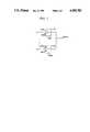
- FIG. 1is a circuit diagram showing a conventional analog multiplexer
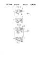
- FIGS. 2 and 3are circuit diagrams showing analog multiplexers in first and second embodiments according to the invention.
- FIG. 4is a timing chart showing an operation of the invention.
- FIG. 5is a circuit diagram showing an analog multiplexer in a third embodiment according to the invention.
- the analog multiplexercomprises (n+1) MOS FET circuits correspondingly connected to (n+1) input terminals Io to In and commonly connected an output terminal MPXO.
- Q501is an n-channel MOS FET
- Q502is a p-channel MOS FET.
- n and p-channel MOS FETsare connected to face each other wherein a selection signal So is applied to a gate electrode of the n-channel MOS FET Q501 and to an inverter N501, an output of which is applied to a gate electrode of the p-channel MOS FET Q502.
- a selection signal Sois applied to a gate electrode of the n-channel MOS FET Q501 and to an inverter N501, an output of which is applied to a gate electrode of the p-channel MOS FET Q502.
- Q503is an n-channel MOS FET
- Q504is a p-channel MOS FET.
- n and p-channel MOS FETsare connected to face each other wherein a selection signal Sn is applied to a gate electrode of the n-channel MOS FET Q503 and to an inverter N502, an output of which is applied to a gate electrode of the p-channel MOS FET Q504.
- input terminals I 1 to I n-1 and MOS FET circuits connected theretoare not shown in FIG. 1, they are of the same circuit structure as explained above.
- the output of the inverter N501is "0", so that the n and p-MOS FETs Q501 and Q502 are turned on, whereby an analog signal level at the input terminal Io is transmitted through the turned-on MOS FET circuit to the output terminal MPXO.
- the selection signal Sois "0”
- the output of the inverter N501is "1”, so that the n and p-MOS FETs Q501 and Q502 are turned off, whereby the analog signal level at the input terminal Io is not transmitted to the output terminal MPXO.
- the n and p-MOS FETs Q503 and Q504are turned on, where the selection signal Sn is "1", while the n and p-MOS FETs Q503 and Q504 are turned off, where the selection signal Sn is "0".
- the analog signal levels at the input terminals Io to Inare controlled to be transmitted to the output terminal MPXO dependent on a content of the selection signals So to Sn.
- FIG. 2shows an analog multiplexer in a first embodiment according to the invention which comprises MOS FET circuits of (n+1) in number correspondingly connected to input terminals of (n+1) in number and commonly connected to an output terminal MPXO.
- MOS FET circuitsconnected to the input terminal Io
- n and p-channel MOS FETs Q101 and Q104are connected to face each other to provide a first MOS FET pair
- n and p-channel MOS FETs Q102 and Q105are connected to face each other to provide a second MOS FET pair, wherein the first and second MOS FET pairs are connected in series
- an n-channel MOS FET Q103is inserted between a connecting point A of the first and second MOS FET pairs and the ground.
- a selection signal Sois applied to gate electrodes of the n-channel MOS FETs Q101 and Q102 and to an inverter N101, an output of which is applied to gate electrodes of the MOS FETs Q103, Q104 and Q105.
- the MOS FET circuit connected to the input terminal Inis of the same circuit structure as that connected to the input terminal Io, wherein Q106, Q107 and Q108 are n-channel MOS FETs, Q109 and Q110 are p-channel MOS FETs, N102 is an inverter, and Sn is a selection signal.
- the MOS FETs Q101, Q102, Q104 and Q105are turned off, and the MOS FET Q103 is turned on, so that an output level at the output terminal MPXO is not affected due to the connecting point A connected to the ground even if an input signal level at the input terminal Io is changed.
- the selection signal Snis "1”
- the MOS FETs Q106, Q107, Q109 and Q110are turned on, and the MOS FET Q108 is turned off.
- the MOS FETs Q106, Q107, Q109 and Q110are turned off, and the MOS FET Q108 is turned on so that a connecting point between a first MOS FET pair Q106 and Q109 and a second MOS FET pair Q107 and Q110 is connected to the ground.
- FIG. 3shows an analog multiplexer in a second embodiment according to the invention.
- Q201 to Q204 and Q207 to Q210are n-channel MOS FETs
- Q205, Q206, Q211 and Q212are p-channel MOS FETs
- N201 and N202are inverters.
- the n-channel MOS FETs Q204 and Q210, to gate electrodes of which a control signal OFF is applied,are added to the circuit structure of the first embodiment.
- control signal OFF of "0"is applied to the MOS FETs Q204 and Q210 during a predetermined duration including times t 1 to t 4 at which the selection signals So and Sn rise up and fall down, so that the ground potential is prevented from being supplied to the input terminals Io to In at respective transient times.
- FIG. 5shows an analog multiplexer in a third embodiment according to the invention.
- the analog multiplexeris the same circuit structure as that in the second embodiment, except that a connecting point A between first and second MOS FET pairs is connected to a power supply potential VDD, where the selection signals So to Sn are "0".
- Q401, Q402, Q407 and Q408are n-channel MOS FETs
- Q403 to Q406 and Q409 to Q412are p-channel MOS FETs
- N401 and N402are inverters.
Landscapes
- Electronic Switches (AREA)
Abstract
Description
Claims (7)
Applications Claiming Priority (2)
| Application Number | Priority Date | Filing Date | Title |
|---|---|---|---|
| JP63023482AJP2600753B2 (en) | 1988-02-03 | 1988-02-03 | Input circuit |
| JP63-23482 | 1988-02-03 |
Publications (1)
| Publication Number | Publication Date |
|---|---|
| US4985703Atrue US4985703A (en) | 1991-01-15 |
Family
ID=12111745
Family Applications (1)
| Application Number | Title | Priority Date | Filing Date |
|---|---|---|---|
| US07/305,538Expired - LifetimeUS4985703A (en) | 1988-02-03 | 1989-02-02 | Analog multiplexer |
Country Status (2)
| Country | Link |
|---|---|
| US (1) | US4985703A (en) |
| JP (1) | JP2600753B2 (en) |
Cited By (95)
| Publication number | Priority date | Publication date | Assignee | Title |
|---|---|---|---|---|
| US5087826A (en)* | 1990-12-28 | 1992-02-11 | Intel Corporation | Multi-layer neural network employing multiplexed output neurons |
| US5323064A (en)* | 1993-04-26 | 1994-06-21 | Raytheon Company | Radio frequency signal frequency converter |
| US5410192A (en)* | 1992-07-09 | 1995-04-25 | Kabushiki Kaisha Toshiba | Potential data selection circuit |
| US5598114A (en)* | 1995-09-27 | 1997-01-28 | Intel Corporation | High speed reduced area multiplexer |
| US5617055A (en)* | 1994-07-29 | 1997-04-01 | Sgs-Thomson Microelectronics S.R.L. | Electronic switch having reduced body effect |
| US5625303A (en)* | 1995-09-27 | 1997-04-29 | Intel Corporation | Multiplexer having a plurality of internal data paths that operate at different speeds |
| US5635745A (en)* | 1994-09-08 | 1997-06-03 | National Semiconductor Corporation | Analog multiplexer cell for mixed digital and analog signal inputs |
| US5646558A (en)* | 1995-09-27 | 1997-07-08 | Intel Corporation | Plurality of distinct multiplexers that operate as a single multiplexer |
| GB2319128A (en)* | 1996-10-30 | 1998-05-13 | Motorola Gmbh | A CMOS transmission gate multiplexer with improved OFF isolation |
| US5789966A (en)* | 1996-09-18 | 1998-08-04 | International Business Machines Corporation | Distributed multiplexer |
| US5796288A (en)* | 1995-05-16 | 1998-08-18 | Hewlett-Packard Company | Graphics accelerator having minimal logic multiplexer system for sharing a microprocessor |
| US5825235A (en)* | 1995-05-15 | 1998-10-20 | Hyundai Electronic Industries, Co., Ltd. | Multiplexer for semiconductor memory device |
| US5872477A (en)* | 1997-06-13 | 1999-02-16 | Vtc Inc. | Multiplexer with CMOS break-before-make circuit |
| US6233650B1 (en)* | 1998-04-01 | 2001-05-15 | Intel Corporation | Using FET switches for large memory arrays |
| US6466072B1 (en)* | 1998-03-30 | 2002-10-15 | Cypress Semiconductor Corp. | Integrated circuitry for display generation |
| US20030081392A1 (en)* | 2001-10-26 | 2003-05-01 | Staktek Group, L.P. | Integrated circuit stacking system and method |
| US20030111736A1 (en)* | 2001-12-14 | 2003-06-19 | Roeters Glen E. | Csp chip stack with flex circuit |
| KR100396637B1 (en)* | 1998-05-13 | 2003-09-02 | 지멘스 악티엔게젤샤프트 | Optimal lag time multiplexer |
| US20030234443A1 (en)* | 2001-10-26 | 2003-12-25 | Staktek Group, L.P. | Low profile stacking system and method |
| US20040000707A1 (en)* | 2001-10-26 | 2004-01-01 | Staktek Group, L.P. | Modularized die stacking system and method |
| US20040000708A1 (en)* | 2001-10-26 | 2004-01-01 | Staktek Group, L.P. | Memory expansion and chip scale stacking system and method |
| US20040052060A1 (en)* | 2001-10-26 | 2004-03-18 | Staktek Group, L.P. | Low profile chip scale stacking system and method |
| US20040061545A1 (en)* | 2002-09-27 | 2004-04-01 | Cosmin Iorga | Timing generator with low delay multiplexer |
| US20040195666A1 (en)* | 2001-10-26 | 2004-10-07 | Julian Partridge | Stacked module systems and methods |
| US20040201091A1 (en)* | 2001-10-26 | 2004-10-14 | Staktek Group, L.P. | Stacked module systems and methods |
| US20040235222A1 (en)* | 2001-10-26 | 2004-11-25 | Staktek Group, L.P. | Integrated circuit stacking system and method |
| US20040245615A1 (en)* | 2003-06-03 | 2004-12-09 | Staktek Group, L.P. | Point to point memory expansion system and method |
| US20040263236A1 (en)* | 2003-06-30 | 2004-12-30 | Morf Thomas E. | Multiplexer and demultiplexer |
| US20050009234A1 (en)* | 2001-10-26 | 2005-01-13 | Staktek Group, L.P. | Stacked module systems and methods for CSP packages |
| US20050018412A1 (en)* | 2001-10-26 | 2005-01-27 | Staktek Group, L.P. | Pitch change and chip scale stacking system |
| US20050057911A1 (en)* | 2003-09-15 | 2005-03-17 | Staktek Group, L.P. | Memory expansion and integrated circuit stacking system and method |
| US20050056921A1 (en)* | 2003-09-15 | 2005-03-17 | Staktek Group L.P. | Stacked module systems and methods |
| US20050083108A1 (en)* | 2000-11-13 | 2005-04-21 | Sami Kiriaki | Analog multiplexers with CMOS control signals |
| US20050139980A1 (en)* | 1992-12-11 | 2005-06-30 | Burns Carmen D. | High density integrated circuit module |
| US20050146011A1 (en)* | 2001-10-26 | 2005-07-07 | Staktek Group, L.P. | Pitch change and chip scale stacking system and method |
| US20060033187A1 (en)* | 2004-08-12 | 2006-02-16 | Staktek Group, L.P. | Rugged CSP module system and method |
| US20060043558A1 (en)* | 2004-09-01 | 2006-03-02 | Staktek Group L.P. | Stacked integrated circuit cascade signaling system and method |
| US20060050497A1 (en)* | 2004-09-03 | 2006-03-09 | Staktek Group L.P. | Buffered thin module system and method |
| US20060049502A1 (en)* | 2004-09-03 | 2006-03-09 | Staktek Group, L.P. | Module thermal management system and method |
| US20060050492A1 (en)* | 2004-09-03 | 2006-03-09 | Staktek Group, L.P. | Thin module system and method |
| US20060050498A1 (en)* | 2004-09-03 | 2006-03-09 | Staktek Group L.P. | Die module system and method |
| US20060050488A1 (en)* | 2004-09-03 | 2006-03-09 | Staktel Group, L.P. | High capacity thin module system and method |
| US20060049513A1 (en)* | 2004-09-03 | 2006-03-09 | Staktek Group L.P. | Thin module system and method with thermal management |
| US20060050592A1 (en)* | 2004-09-03 | 2006-03-09 | Staktek Group L.P. | Compact module system and method |
| US20060049500A1 (en)* | 2004-09-03 | 2006-03-09 | Staktek Group L.P. | Thin module system and method |
| US20060055024A1 (en)* | 2004-09-14 | 2006-03-16 | Staktek Group, L.P. | Adapted leaded integrated circuit module |
| US20060072297A1 (en)* | 2004-10-01 | 2006-04-06 | Staktek Group L.P. | Circuit Module Access System and Method |
| US7033861B1 (en) | 2005-05-18 | 2006-04-25 | Staktek Group L.P. | Stacked module systems and method |
| US20060118936A1 (en)* | 2004-12-03 | 2006-06-08 | Staktek Group L.P. | Circuit module component mounting system and method |
| US20060131716A1 (en)* | 2001-10-26 | 2006-06-22 | Cady James W | Stacking system and method |
| US20060157842A1 (en)* | 2005-01-20 | 2006-07-20 | Staktek Group L.P. | Inverted CSP stacking system and method |
| US20060170459A1 (en)* | 2005-01-31 | 2006-08-03 | Samsung Electronics Co., Ltd. | Multiplexer and methods thereof |
| US20060175693A1 (en)* | 2005-02-04 | 2006-08-10 | Staktek Group, L.P. | Systems, methods, and apparatus for generating ball-out matrix configuration output for a flex circuit |
| US20060198238A1 (en)* | 2004-09-03 | 2006-09-07 | Staktek Group L.P. | Modified core for circuit module system and method |
| US20060203442A1 (en)* | 2004-09-03 | 2006-09-14 | Staktek Group, L.P. | Memory module system and method |
| US20060244114A1 (en)* | 2005-04-28 | 2006-11-02 | Staktek Group L.P. | Systems, methods, and apparatus for connecting a set of contacts on an integrated circuit to a flex circuit via a contact beam |
| US20060250780A1 (en)* | 2005-05-06 | 2006-11-09 | Staktek Group L.P. | System component interposer |
| US20060255446A1 (en)* | 2001-10-26 | 2006-11-16 | Staktek Group, L.P. | Stacked modules and method |
| US20060261449A1 (en)* | 2005-05-18 | 2006-11-23 | Staktek Group L.P. | Memory module system and method |
| US20070103877A1 (en)* | 2005-11-04 | 2007-05-10 | Staktek Group L.P. | Flex circuit apparatus and method for adding capacitance while conserving circuit board surface area |
| USRE39628E1 (en) | 1999-05-05 | 2007-05-15 | Stakick Group, L.P. | Stackable flex circuit IC package and method of making same |
| US20070158821A1 (en)* | 2006-01-11 | 2007-07-12 | Leland Szewerenko | Managed memory component |
| US20070158802A1 (en)* | 2006-01-11 | 2007-07-12 | Staktek Group L.P. | High density memory card system and method |
| US20070164416A1 (en)* | 2006-01-17 | 2007-07-19 | James Douglas Wehrly | Managed memory component |
| US20070170561A1 (en)* | 2006-01-11 | 2007-07-26 | Staktek Group L.P. | Leaded package integrated circuit stacking |
| US20070176286A1 (en)* | 2006-02-02 | 2007-08-02 | Staktek Group L.P. | Composite core circuit module system and method |
| US20070201208A1 (en)* | 2006-02-27 | 2007-08-30 | Staktek Group L.P. | Active cooling methods and apparatus for modules |
| US20070262429A1 (en)* | 2006-05-15 | 2007-11-15 | Staktek Group, L.P. | Perimeter stacking system and method |
| US7304382B2 (en) | 2006-01-11 | 2007-12-04 | Staktek Group L.P. | Managed memory component |
| US7310458B2 (en) | 2001-10-26 | 2007-12-18 | Staktek Group L.P. | Stacked module systems and methods |
| US20080030255A1 (en)* | 2006-08-02 | 2008-02-07 | Nec Electronics Corporation | Switch circuit and switch device |
| US20080093724A1 (en)* | 2006-10-20 | 2008-04-24 | Staktek Group L.P. | Stackable Micropackages and Stacked Modules |
| US7417310B2 (en) | 2006-11-02 | 2008-08-26 | Entorian Technologies, Lp | Circuit module having force resistant construction |
| US7443023B2 (en) | 2004-09-03 | 2008-10-28 | Entorian Technologies, Lp | High capacity thin module system |
| US7446410B2 (en) | 2004-09-03 | 2008-11-04 | Entorian Technologies, Lp | Circuit module with thermal casing systems |
| US7508069B2 (en) | 2006-01-11 | 2009-03-24 | Entorian Technologies, Lp | Managed memory component |
| US7522421B2 (en) | 2004-09-03 | 2009-04-21 | Entorian Technologies, Lp | Split core circuit module |
| US7542297B2 (en) | 2004-09-03 | 2009-06-02 | Entorian Technologies, Lp | Optimized mounting area circuit module system and method |
| US7579687B2 (en) | 2004-09-03 | 2009-08-25 | Entorian Technologies, Lp | Circuit module turbulence enhancement systems and methods |
| US7605454B2 (en) | 2006-01-11 | 2009-10-20 | Entorian Technologies, Lp | Memory card and method for devising |
| US7616452B2 (en) | 2004-09-03 | 2009-11-10 | Entorian Technologies, Lp | Flex circuit constructions for high capacity circuit module systems and methods |
| USRE41039E1 (en) | 2000-01-13 | 2009-12-15 | Entorian Technologies, Lp | Stackable chip package with flex carrier |
| US7656678B2 (en) | 2001-10-26 | 2010-02-02 | Entorian Technologies, Lp | Stacked module systems |
| US20110098382A1 (en)* | 2008-04-09 | 2011-04-28 | Zephyros Inc | Structural adhesives |
| US20120056661A1 (en)* | 2010-09-08 | 2012-03-08 | Ayman Shabra | High voltage multiplexer element and multiplexer system using same |
| US20130009623A1 (en)* | 2009-11-16 | 2013-01-10 | Analog Devices, Inc. | Four-quadrant bootstrapped switch circuit |
| US20130057334A1 (en)* | 2011-06-20 | 2013-03-07 | St Ericsson Sa | Method for providing a system on chip with power and body bias voltages |
| CN103597746A (en)* | 2011-06-16 | 2014-02-19 | 罗姆股份有限公司 | Analog switch circuit and motor drive device using it |
| TWI427883B (en)* | 2006-12-01 | 2014-02-21 | Nokia Corp | Over-voltage protection circuit, method and computer program product for operating the same and mobile device |
| US8766701B1 (en)* | 2013-03-08 | 2014-07-01 | Xilinx, Inc. | Analog multiplexing with independent power supplies |
| US9013228B2 (en) | 2011-06-20 | 2015-04-21 | Stmicroelectronics Sa | Method for providing a system on chip with power and body bias voltages |
| US20150222268A1 (en)* | 2014-01-31 | 2015-08-06 | Texas Instruments Deutschland Gmbh | Configurable analog front ends for circuits with substantially gate enclosed inner electrode mosfet switch |
| US20160218710A1 (en)* | 2015-01-23 | 2016-07-28 | Seiko Instruments Inc. | Switch circuit |
| US9444451B2 (en) | 2012-02-29 | 2016-09-13 | Sii Semiconductor Corporation | Switch circuit |
| US11106235B2 (en)* | 2019-09-13 | 2021-08-31 | Silicon Laboratories Inc. | Configurable clock buffer for multiple operating modes |
Families Citing this family (1)
| Publication number | Priority date | Publication date | Assignee | Title |
|---|---|---|---|---|
| JPH01236731A (en)* | 1988-03-16 | 1989-09-21 | Nec Corp | Complementary analog switch |
Citations (4)
| Publication number | Priority date | Publication date | Assignee | Title |
|---|---|---|---|---|
| US4551634A (en)* | 1982-03-31 | 1985-11-05 | Fujitsu Limited | Multiplexing input circuit |
| US4556804A (en)* | 1983-11-17 | 1985-12-03 | Motorola, Inc. | Power multiplexer switch and method |
| US4645944A (en)* | 1983-09-05 | 1987-02-24 | Matsushita Electric Industrial Co., Ltd. | MOS register for selecting among various data inputs |
| US4695749A (en)* | 1986-02-25 | 1987-09-22 | Fairchild Semiconductor Corporation | Emitter-coupled logic multiplexer |
Family Cites Families (2)
| Publication number | Priority date | Publication date | Assignee | Title |
|---|---|---|---|---|
| JPS6154711A (en)* | 1984-08-27 | 1986-03-19 | Yokogawa Hokushin Electric Corp | analog switch |
| JPS61192121A (en)* | 1985-02-20 | 1986-08-26 | New Japan Radio Co Ltd | Switch circuit for analog signal |
- 1988
- 1988-02-03JPJP63023482Apatent/JP2600753B2/ennot_activeExpired - Lifetime
- 1989
- 1989-02-02USUS07/305,538patent/US4985703A/ennot_activeExpired - Lifetime
Patent Citations (4)
| Publication number | Priority date | Publication date | Assignee | Title |
|---|---|---|---|---|
| US4551634A (en)* | 1982-03-31 | 1985-11-05 | Fujitsu Limited | Multiplexing input circuit |
| US4645944A (en)* | 1983-09-05 | 1987-02-24 | Matsushita Electric Industrial Co., Ltd. | MOS register for selecting among various data inputs |
| US4556804A (en)* | 1983-11-17 | 1985-12-03 | Motorola, Inc. | Power multiplexer switch and method |
| US4695749A (en)* | 1986-02-25 | 1987-09-22 | Fairchild Semiconductor Corporation | Emitter-coupled logic multiplexer |
Cited By (182)
| Publication number | Priority date | Publication date | Assignee | Title |
|---|---|---|---|---|
| US5087826A (en)* | 1990-12-28 | 1992-02-11 | Intel Corporation | Multi-layer neural network employing multiplexed output neurons |
| US5410192A (en)* | 1992-07-09 | 1995-04-25 | Kabushiki Kaisha Toshiba | Potential data selection circuit |
| US20050139980A1 (en)* | 1992-12-11 | 2005-06-30 | Burns Carmen D. | High density integrated circuit module |
| US5323064A (en)* | 1993-04-26 | 1994-06-21 | Raytheon Company | Radio frequency signal frequency converter |
| US5617055A (en)* | 1994-07-29 | 1997-04-01 | Sgs-Thomson Microelectronics S.R.L. | Electronic switch having reduced body effect |
| US5635745A (en)* | 1994-09-08 | 1997-06-03 | National Semiconductor Corporation | Analog multiplexer cell for mixed digital and analog signal inputs |
| US5639680A (en)* | 1994-09-08 | 1997-06-17 | National Semiconductor Corporation | Method of making analog multiplexer cell for mixed digital and analog signal inputs |
| GB2300939B (en)* | 1995-05-15 | 1999-11-03 | Hyundai Electronics Ind | Multiplexer for semiconductor memory device |
| US5825235A (en)* | 1995-05-15 | 1998-10-20 | Hyundai Electronic Industries, Co., Ltd. | Multiplexer for semiconductor memory device |
| US5796288A (en)* | 1995-05-16 | 1998-08-18 | Hewlett-Packard Company | Graphics accelerator having minimal logic multiplexer system for sharing a microprocessor |
| US5646558A (en)* | 1995-09-27 | 1997-07-08 | Intel Corporation | Plurality of distinct multiplexers that operate as a single multiplexer |
| US5625303A (en)* | 1995-09-27 | 1997-04-29 | Intel Corporation | Multiplexer having a plurality of internal data paths that operate at different speeds |
| US5598114A (en)* | 1995-09-27 | 1997-01-28 | Intel Corporation | High speed reduced area multiplexer |
| US5789966A (en)* | 1996-09-18 | 1998-08-04 | International Business Machines Corporation | Distributed multiplexer |
| GB2319128A (en)* | 1996-10-30 | 1998-05-13 | Motorola Gmbh | A CMOS transmission gate multiplexer with improved OFF isolation |
| US5872477A (en)* | 1997-06-13 | 1999-02-16 | Vtc Inc. | Multiplexer with CMOS break-before-make circuit |
| US6466072B1 (en)* | 1998-03-30 | 2002-10-15 | Cypress Semiconductor Corp. | Integrated circuitry for display generation |
| US6233650B1 (en)* | 1998-04-01 | 2001-05-15 | Intel Corporation | Using FET switches for large memory arrays |
| KR100396637B1 (en)* | 1998-05-13 | 2003-09-02 | 지멘스 악티엔게젤샤프트 | Optimal lag time multiplexer |
| USRE39628E1 (en) | 1999-05-05 | 2007-05-15 | Stakick Group, L.P. | Stackable flex circuit IC package and method of making same |
| USRE41039E1 (en) | 2000-01-13 | 2009-12-15 | Entorian Technologies, Lp | Stackable chip package with flex carrier |
| US20050083108A1 (en)* | 2000-11-13 | 2005-04-21 | Sami Kiriaki | Analog multiplexers with CMOS control signals |
| US20080067662A1 (en)* | 2001-10-26 | 2008-03-20 | Staktek Group L.P. | Modularized Die Stacking System and Method |
| US7371609B2 (en) | 2001-10-26 | 2008-05-13 | Staktek Group L.P. | Stacked module systems and methods |
| US7586758B2 (en) | 2001-10-26 | 2009-09-08 | Entorian Technologies, Lp | Integrated circuit stacking system |
| US20040197956A1 (en)* | 2001-10-26 | 2004-10-07 | Staktek Group L.P. | Memory expansion and chip scale stacking system and method |
| US20040195666A1 (en)* | 2001-10-26 | 2004-10-07 | Julian Partridge | Stacked module systems and methods |
| US20040201091A1 (en)* | 2001-10-26 | 2004-10-14 | Staktek Group, L.P. | Stacked module systems and methods |
| US20040235222A1 (en)* | 2001-10-26 | 2004-11-25 | Staktek Group, L.P. | Integrated circuit stacking system and method |
| US7572671B2 (en) | 2001-10-26 | 2009-08-11 | Entorian Technologies, Lp | Stacked module systems and methods |
| US7524703B2 (en) | 2001-10-26 | 2009-04-28 | Entorian Technologies, Lp | Integrated circuit stacking system and method |
| US20050009234A1 (en)* | 2001-10-26 | 2005-01-13 | Staktek Group, L.P. | Stacked module systems and methods for CSP packages |
| US20050018412A1 (en)* | 2001-10-26 | 2005-01-27 | Staktek Group, L.P. | Pitch change and chip scale stacking system |
| US20050041404A1 (en)* | 2001-10-26 | 2005-02-24 | Staktek Group. L.P. | Integrated circuit stacking system and method |
| US20050041403A1 (en)* | 2001-10-26 | 2005-02-24 | Staktek Group, L.P. | Integrated circuit stacking system and method |
| US20050041402A1 (en)* | 2001-10-26 | 2005-02-24 | Staktek Group, L.P. | Integrated circuit stacking system and method |
| US7606048B2 (en) | 2001-10-26 | 2009-10-20 | Enthorian Technologies, LP | Integrated circuit stacking system |
| US7495334B2 (en) | 2001-10-26 | 2009-02-24 | Entorian Technologies, Lp | Stacking system and method |
| US20050067683A1 (en)* | 2001-10-26 | 2005-03-31 | Staktek Group L.P. | Memory expansion and chip scale stacking system and method |
| US20040000708A1 (en)* | 2001-10-26 | 2004-01-01 | Staktek Group, L.P. | Memory expansion and chip scale stacking system and method |
| US7485951B2 (en) | 2001-10-26 | 2009-02-03 | Entorian Technologies, Lp | Modularized die stacking system and method |
| US20040000707A1 (en)* | 2001-10-26 | 2004-01-01 | Staktek Group, L.P. | Modularized die stacking system and method |
| US6914324B2 (en) | 2001-10-26 | 2005-07-05 | Staktek Group L.P. | Memory expansion and chip scale stacking system and method |
| US20050146031A1 (en)* | 2001-10-26 | 2005-07-07 | Staktek Group, L.P. | Low profile stacking system and method |
| US20050146011A1 (en)* | 2001-10-26 | 2005-07-07 | Staktek Group, L.P. | Pitch change and chip scale stacking system and method |
| US6940729B2 (en) | 2001-10-26 | 2005-09-06 | Staktek Group L.P. | Integrated circuit stacking system and method |
| US6955945B2 (en) | 2001-10-26 | 2005-10-18 | Staktek Group L.P. | Memory expansion and chip scale stacking system and method |
| US20050242423A1 (en)* | 2001-10-26 | 2005-11-03 | Staktek Group, L.P. | Stacked module systems and methods |
| US20050263872A1 (en)* | 2001-10-26 | 2005-12-01 | Cady James W | Flex-based circuit module |
| US20050280135A1 (en)* | 2001-10-26 | 2005-12-22 | Staktek Group L.P. | Stacking system and method |
| US20090273069A1 (en)* | 2001-10-26 | 2009-11-05 | Cady James W | Low profile chip scale stacking system and method |
| US20080120831A1 (en)* | 2001-10-26 | 2008-05-29 | Staktek Group L.P. | Stacked Modules and Method |
| US20040052060A1 (en)* | 2001-10-26 | 2004-03-18 | Staktek Group, L.P. | Low profile chip scale stacking system and method |
| US20080090329A1 (en)* | 2001-10-26 | 2008-04-17 | Staktek Group L.P. | Stacked Modules and Method |
| US20080088032A1 (en)* | 2001-10-26 | 2008-04-17 | Staktek Group L.P. | Stacked Modules and Method |
| US20080088003A1 (en)* | 2001-10-26 | 2008-04-17 | Staktek Group L.P. | Stacked Modules and Method |
| US7595550B2 (en) | 2001-10-26 | 2009-09-29 | Entorian Technologies, Lp | Flex-based circuit module |
| US7335975B2 (en) | 2001-10-26 | 2008-02-26 | Staktek Group L.P. | Integrated circuit stacking system and method |
| US7310458B2 (en) | 2001-10-26 | 2007-12-18 | Staktek Group L.P. | Stacked module systems and methods |
| US7626273B2 (en) | 2001-10-26 | 2009-12-01 | Entorian Technologies, L.P. | Low profile stacking system and method |
| US20090298230A1 (en)* | 2001-10-26 | 2009-12-03 | Staktek Group, L.P. | Stacked Module Systems and Methods |
| US20030081392A1 (en)* | 2001-10-26 | 2003-05-01 | Staktek Group, L.P. | Integrated circuit stacking system and method |
| US7656678B2 (en) | 2001-10-26 | 2010-02-02 | Entorian Technologies, Lp | Stacked module systems |
| US7026708B2 (en) | 2001-10-26 | 2006-04-11 | Staktek Group L.P. | Low profile chip scale stacking system and method |
| US7256484B2 (en) | 2001-10-26 | 2007-08-14 | Staktek Group L.P. | Memory expansion and chip scale stacking system and method |
| US7053478B2 (en) | 2001-10-26 | 2006-05-30 | Staktek Group L.P. | Pitch change and chip scale stacking system |
| US7719098B2 (en) | 2001-10-26 | 2010-05-18 | Entorian Technologies Lp | Stacked modules and method |
| US20060131716A1 (en)* | 2001-10-26 | 2006-06-22 | Cady James W | Stacking system and method |
| US20070114649A1 (en)* | 2001-10-26 | 2007-05-24 | Staktek Group L.P., A Texas Limited Partnership | Low Profile Stacking System and Method |
| US20070117262A1 (en)* | 2001-10-26 | 2007-05-24 | Staktek Group L.P., A Texas Limited Partnership | Low Profile Stacking System and Method |
| US20030234443A1 (en)* | 2001-10-26 | 2003-12-25 | Staktek Group, L.P. | Low profile stacking system and method |
| US7202555B2 (en) | 2001-10-26 | 2007-04-10 | Staktek Group L.P. | Pitch change and chip scale stacking system and method |
| US7180167B2 (en) | 2001-10-26 | 2007-02-20 | Staktek Group L. P. | Low profile stacking system and method |
| US7094632B2 (en) | 2001-10-26 | 2006-08-22 | Staktek Group L.P. | Low profile chip scale stacking system and method |
| US20060255446A1 (en)* | 2001-10-26 | 2006-11-16 | Staktek Group, L.P. | Stacked modules and method |
| US20030111736A1 (en)* | 2001-12-14 | 2003-06-19 | Roeters Glen E. | Csp chip stack with flex circuit |
| US7081373B2 (en) | 2001-12-14 | 2006-07-25 | Staktek Group, L.P. | CSP chip stack with flex circuit |
| US7193310B2 (en) | 2001-12-14 | 2007-03-20 | Stuktek Group L.P. | Stacking system and method |
| US20040061545A1 (en)* | 2002-09-27 | 2004-04-01 | Cosmin Iorga | Timing generator with low delay multiplexer |
| US20040245615A1 (en)* | 2003-06-03 | 2004-12-09 | Staktek Group, L.P. | Point to point memory expansion system and method |
| US7088170B2 (en)* | 2003-06-30 | 2006-08-08 | International Business Machines Corporation | Multiplexer and demultiplexer |
| US20040263236A1 (en)* | 2003-06-30 | 2004-12-30 | Morf Thomas E. | Multiplexer and demultiplexer |
| US7542304B2 (en) | 2003-09-15 | 2009-06-02 | Entorian Technologies, Lp | Memory expansion and integrated circuit stacking system and method |
| US20050056921A1 (en)* | 2003-09-15 | 2005-03-17 | Staktek Group L.P. | Stacked module systems and methods |
| US20050098873A1 (en)* | 2003-09-15 | 2005-05-12 | Staktek Group L.P. | Stacked module systems and methods |
| US20050057911A1 (en)* | 2003-09-15 | 2005-03-17 | Staktek Group, L.P. | Memory expansion and integrated circuit stacking system and method |
| US20060033187A1 (en)* | 2004-08-12 | 2006-02-16 | Staktek Group, L.P. | Rugged CSP module system and method |
| US20060043558A1 (en)* | 2004-09-01 | 2006-03-02 | Staktek Group L.P. | Stacked integrated circuit cascade signaling system and method |
| US7760513B2 (en) | 2004-09-03 | 2010-07-20 | Entorian Technologies Lp | Modified core for circuit module system and method |
| US7443023B2 (en) | 2004-09-03 | 2008-10-28 | Entorian Technologies, Lp | High capacity thin module system |
| US7579687B2 (en) | 2004-09-03 | 2009-08-25 | Entorian Technologies, Lp | Circuit module turbulence enhancement systems and methods |
| US20060203442A1 (en)* | 2004-09-03 | 2006-09-14 | Staktek Group, L.P. | Memory module system and method |
| US7737549B2 (en) | 2004-09-03 | 2010-06-15 | Entorian Technologies Lp | Circuit module with thermal casing systems |
| US7602613B2 (en) | 2004-09-03 | 2009-10-13 | Entorian Technologies, Lp | Thin module system and method |
| US7606050B2 (en) | 2004-09-03 | 2009-10-20 | Entorian Technologies, Lp | Compact module system and method |
| US20060198238A1 (en)* | 2004-09-03 | 2006-09-07 | Staktek Group L.P. | Modified core for circuit module system and method |
| US7542297B2 (en) | 2004-09-03 | 2009-06-02 | Entorian Technologies, Lp | Optimized mounting area circuit module system and method |
| US20060050496A1 (en)* | 2004-09-03 | 2006-03-09 | Staktek Group L.P. | Thin module system and method |
| US20060049500A1 (en)* | 2004-09-03 | 2006-03-09 | Staktek Group L.P. | Thin module system and method |
| US20060050592A1 (en)* | 2004-09-03 | 2006-03-09 | Staktek Group L.P. | Compact module system and method |
| US7522421B2 (en) | 2004-09-03 | 2009-04-21 | Entorian Technologies, Lp | Split core circuit module |
| US7522425B2 (en) | 2004-09-03 | 2009-04-21 | Entorian Technologies, Lp | High capacity thin module system and method |
| US7324352B2 (en) | 2004-09-03 | 2008-01-29 | Staktek Group L.P. | High capacity thin module system and method |
| US20080030966A1 (en)* | 2004-09-03 | 2008-02-07 | Staktek Group L.P. | High Capacity Thin Module System and Method |
| US7626259B2 (en) | 2004-09-03 | 2009-12-01 | Entorian Technologies, Lp | Heat sink for a high capacity thin module system |
| US20060049513A1 (en)* | 2004-09-03 | 2006-03-09 | Staktek Group L.P. | Thin module system and method with thermal management |
| US20060050488A1 (en)* | 2004-09-03 | 2006-03-09 | Staktel Group, L.P. | High capacity thin module system and method |
| US20060050498A1 (en)* | 2004-09-03 | 2006-03-09 | Staktek Group L.P. | Die module system and method |
| US20060050492A1 (en)* | 2004-09-03 | 2006-03-09 | Staktek Group, L.P. | Thin module system and method |
| US20060049502A1 (en)* | 2004-09-03 | 2006-03-09 | Staktek Group, L.P. | Module thermal management system and method |
| US7616452B2 (en) | 2004-09-03 | 2009-11-10 | Entorian Technologies, Lp | Flex circuit constructions for high capacity circuit module systems and methods |
| US20060050497A1 (en)* | 2004-09-03 | 2006-03-09 | Staktek Group L.P. | Buffered thin module system and method |
| US7606049B2 (en) | 2004-09-03 | 2009-10-20 | Entorian Technologies, Lp | Module thermal management system and method |
| US7511968B2 (en) | 2004-09-03 | 2009-03-31 | Entorian Technologies, Lp | Buffered thin module system and method |
| US7423885B2 (en) | 2004-09-03 | 2008-09-09 | Entorian Technologies, Lp | Die module system |
| US7768796B2 (en) | 2004-09-03 | 2010-08-03 | Entorian Technologies L.P. | Die module system |
| US7446410B2 (en) | 2004-09-03 | 2008-11-04 | Entorian Technologies, Lp | Circuit module with thermal casing systems |
| US20080278901A9 (en)* | 2004-09-03 | 2008-11-13 | Staktek Group, L.P. | Memory module system and method |
| US20080278924A1 (en)* | 2004-09-03 | 2008-11-13 | Entorian Technologies, L.P. (Formerly Staktek Group L.P.) | Die module system |
| US7459784B2 (en) | 2004-09-03 | 2008-12-02 | Entorian Technologies, Lp | High capacity thin module system |
| US7606042B2 (en) | 2004-09-03 | 2009-10-20 | Entorian Technologies, Lp | High capacity thin module system and method |
| US7468893B2 (en) | 2004-09-03 | 2008-12-23 | Entorian Technologies, Lp | Thin module system and method |
| US7480152B2 (en) | 2004-09-03 | 2009-01-20 | Entorian Technologies, Lp | Thin module system and method |
| US7606040B2 (en) | 2004-09-03 | 2009-10-20 | Entorian Technologies, Lp | Memory module system and method |
| US20090052124A1 (en)* | 2004-09-03 | 2009-02-26 | Entorian Technologies, L.P. (Formerly Staktek Group, L.P) | Circuit Module with Thermal Casing Systems |
| US20060055024A1 (en)* | 2004-09-14 | 2006-03-16 | Staktek Group, L.P. | Adapted leaded integrated circuit module |
| US20060072297A1 (en)* | 2004-10-01 | 2006-04-06 | Staktek Group L.P. | Circuit Module Access System and Method |
| US20060118936A1 (en)* | 2004-12-03 | 2006-06-08 | Staktek Group L.P. | Circuit module component mounting system and method |
| US20060157842A1 (en)* | 2005-01-20 | 2006-07-20 | Staktek Group L.P. | Inverted CSP stacking system and method |
| US7309914B2 (en) | 2005-01-20 | 2007-12-18 | Staktek Group L.P. | Inverted CSP stacking system and method |
| US20060170459A1 (en)* | 2005-01-31 | 2006-08-03 | Samsung Electronics Co., Ltd. | Multiplexer and methods thereof |
| US20060175693A1 (en)* | 2005-02-04 | 2006-08-10 | Staktek Group, L.P. | Systems, methods, and apparatus for generating ball-out matrix configuration output for a flex circuit |
| US20060244114A1 (en)* | 2005-04-28 | 2006-11-02 | Staktek Group L.P. | Systems, methods, and apparatus for connecting a set of contacts on an integrated circuit to a flex circuit via a contact beam |
| US20060250780A1 (en)* | 2005-05-06 | 2006-11-09 | Staktek Group L.P. | System component interposer |
| US20060261449A1 (en)* | 2005-05-18 | 2006-11-23 | Staktek Group L.P. | Memory module system and method |
| US7033861B1 (en) | 2005-05-18 | 2006-04-25 | Staktek Group L.P. | Stacked module systems and method |
| US7323364B2 (en) | 2005-05-18 | 2008-01-29 | Staktek Group L.P. | Stacked module systems and method |
| US20070126124A1 (en)* | 2005-05-18 | 2007-06-07 | Staktek Group L.P. | Memory Module System and Method |
| US20070126125A1 (en)* | 2005-05-18 | 2007-06-07 | Staktek Group L.P. | Memory Module System and Method |
| US20070103877A1 (en)* | 2005-11-04 | 2007-05-10 | Staktek Group L.P. | Flex circuit apparatus and method for adding capacitance while conserving circuit board surface area |
| US7576995B2 (en) | 2005-11-04 | 2009-08-18 | Entorian Technologies, Lp | Flex circuit apparatus and method for adding capacitance while conserving circuit board surface area |
| US20070158802A1 (en)* | 2006-01-11 | 2007-07-12 | Staktek Group L.P. | High density memory card system and method |
| US7304382B2 (en) | 2006-01-11 | 2007-12-04 | Staktek Group L.P. | Managed memory component |
| US7605454B2 (en) | 2006-01-11 | 2009-10-20 | Entorian Technologies, Lp | Memory card and method for devising |
| US20090170243A1 (en)* | 2006-01-11 | 2009-07-02 | Entorian Technologies, Lp | Stacked Integrated Circuit Module |
| US7508069B2 (en) | 2006-01-11 | 2009-03-24 | Entorian Technologies, Lp | Managed memory component |
| US7508058B2 (en) | 2006-01-11 | 2009-03-24 | Entorian Technologies, Lp | Stacked integrated circuit module |
| US20070158821A1 (en)* | 2006-01-11 | 2007-07-12 | Leland Szewerenko | Managed memory component |
| US7608920B2 (en) | 2006-01-11 | 2009-10-27 | Entorian Technologies, Lp | Memory card and method for devising |
| US20070170561A1 (en)* | 2006-01-11 | 2007-07-26 | Staktek Group L.P. | Leaded package integrated circuit stacking |
| US20090160042A1 (en)* | 2006-01-17 | 2009-06-25 | Entorian Technologies, Lp | Managed Memory Component |
| US20070164416A1 (en)* | 2006-01-17 | 2007-07-19 | James Douglas Wehrly | Managed memory component |
| US20070176286A1 (en)* | 2006-02-02 | 2007-08-02 | Staktek Group L.P. | Composite core circuit module system and method |
| US7511969B2 (en) | 2006-02-02 | 2009-03-31 | Entorian Technologies, Lp | Composite core circuit module system and method |
| US7289327B2 (en) | 2006-02-27 | 2007-10-30 | Stakick Group L.P. | Active cooling methods and apparatus for modules |
| US20070201208A1 (en)* | 2006-02-27 | 2007-08-30 | Staktek Group L.P. | Active cooling methods and apparatus for modules |
| US20070262429A1 (en)* | 2006-05-15 | 2007-11-15 | Staktek Group, L.P. | Perimeter stacking system and method |
| US20080030255A1 (en)* | 2006-08-02 | 2008-02-07 | Nec Electronics Corporation | Switch circuit and switch device |
| US20080093724A1 (en)* | 2006-10-20 | 2008-04-24 | Staktek Group L.P. | Stackable Micropackages and Stacked Modules |
| US7468553B2 (en) | 2006-10-20 | 2008-12-23 | Entorian Technologies, Lp | Stackable micropackages and stacked modules |
| US7417310B2 (en) | 2006-11-02 | 2008-08-26 | Entorian Technologies, Lp | Circuit module having force resistant construction |
| US7804985B2 (en) | 2006-11-02 | 2010-09-28 | Entorian Technologies Lp | Circuit module having force resistant construction |
| TWI427883B (en)* | 2006-12-01 | 2014-02-21 | Nokia Corp | Over-voltage protection circuit, method and computer program product for operating the same and mobile device |
| US20110098382A1 (en)* | 2008-04-09 | 2011-04-28 | Zephyros Inc | Structural adhesives |
| US11667813B2 (en) | 2008-04-09 | 2023-06-06 | Zephyros, Inc. | Structural adhesives |
| US11248145B2 (en) | 2008-04-09 | 2022-02-15 | Zephyros, Inc. | Structural adhesives |
| US20130009623A1 (en)* | 2009-11-16 | 2013-01-10 | Analog Devices, Inc. | Four-quadrant bootstrapped switch circuit |
| US8604862B2 (en)* | 2009-11-16 | 2013-12-10 | Analog Devices, Inc. | Four-quadrant bootstrapped switch circuit |
| US20120056661A1 (en)* | 2010-09-08 | 2012-03-08 | Ayman Shabra | High voltage multiplexer element and multiplexer system using same |
| CN103597746B (en)* | 2011-06-16 | 2016-08-31 | 罗姆股份有限公司 | Analog switch circuit and motor drive device using it |
| CN103597746A (en)* | 2011-06-16 | 2014-02-19 | 罗姆股份有限公司 | Analog switch circuit and motor drive device using it |
| US9013228B2 (en) | 2011-06-20 | 2015-04-21 | Stmicroelectronics Sa | Method for providing a system on chip with power and body bias voltages |
| US20130057334A1 (en)* | 2011-06-20 | 2013-03-07 | St Ericsson Sa | Method for providing a system on chip with power and body bias voltages |
| US9444451B2 (en) | 2012-02-29 | 2016-09-13 | Sii Semiconductor Corporation | Switch circuit |
| TWI575872B (en)* | 2012-02-29 | 2017-03-21 | Sii Semiconductor Corp | Switch circuit |
| CN104137418B (en)* | 2012-02-29 | 2017-06-16 | 精工半导体有限公司 | On-off circuit |
| US8766701B1 (en)* | 2013-03-08 | 2014-07-01 | Xilinx, Inc. | Analog multiplexing with independent power supplies |
| US20150222268A1 (en)* | 2014-01-31 | 2015-08-06 | Texas Instruments Deutschland Gmbh | Configurable analog front ends for circuits with substantially gate enclosed inner electrode mosfet switch |
| US9520880B2 (en)* | 2014-01-31 | 2016-12-13 | Texas Instruments Deutschland Gmbh | Configurable analog front ends for circuits with substantially gate enclosed inner electrode MOSFET switch |
| US20160218710A1 (en)* | 2015-01-23 | 2016-07-28 | Seiko Instruments Inc. | Switch circuit |
| US9571094B2 (en)* | 2015-01-23 | 2017-02-14 | Sii Semiconductor Corporation | Switch circuit |
| US11106235B2 (en)* | 2019-09-13 | 2021-08-31 | Silicon Laboratories Inc. | Configurable clock buffer for multiple operating modes |
Also Published As
| Publication number | Publication date |
|---|---|
| JP2600753B2 (en) | 1997-04-16 |
| JPH01198823A (en) | 1989-08-10 |
Similar Documents
| Publication | Publication Date | Title |
|---|---|---|
| US4985703A (en) | Analog multiplexer | |
| US4656373A (en) | High-speed voltage level shift circuit | |
| EP0703665B1 (en) | Voltage level shift circuit | |
| US5216289A (en) | Asynchronous reset scheme for ultra-low noise port tri-state output driver circuit | |
| US3654394A (en) | Field effect transistor switch, particularly for multiplexing | |
| US3675144A (en) | Transmission gate and biasing circuits | |
| KR950020069A (en) | Data driver | |
| KR910013535A (en) | Semiconductor integrated circuit | |
| JPH06169252A (en) | Programmable logic-circuit device | |
| KR930018850A (en) | Output buffer device | |
| KR880001109A (en) | Integrated Logic Circuit | |
| KR890010906A (en) | Static RAM Output Circuit | |
| US4988894A (en) | Power supply switching circuit | |
| US5170073A (en) | Ultra-low noise port output driver circuit | |
| US4932027A (en) | Single-level multiplexer | |
| KR970063278A (en) | Semiconductor memory | |
| KR950023885A (en) | A voltage selector that receives a plurality of inputs and selectively outputs one of them | |
| DE3685026D1 (en) | CLOCKED CMOS SWITCHING WITH AT LEAST ONE CMOS SWITCH. | |
| JPH0628882A (en) | Sample-hold circuit | |
| KR100236911B1 (en) | Automatic polarity conversion circuit | |
| JPS62145906A (en) | Amplifier circuit | |
| US4571509A (en) | Output circuit having decreased interference between output terminals | |
| US3927365A (en) | Switch operating device | |
| JP2830902B2 (en) | Output buffer circuit | |
| JPS6470996A (en) | Writable sense amplifier for read-only- memory |
Legal Events
| Date | Code | Title | Description |
|---|---|---|---|
| AS | Assignment | Owner name:NEC CORPORATION, JAPAN Free format text:ASSIGNMENT OF ASSIGNORS INTEREST.;ASSIGNOR:KANEYAMA, HIDEYO;REEL/FRAME:005041/0544 Effective date:19890313 | |
| STCF | Information on status: patent grant | Free format text:PATENTED CASE | |
| FEPP | Fee payment procedure | Free format text:PAYOR NUMBER ASSIGNED (ORIGINAL EVENT CODE: ASPN); ENTITY STATUS OF PATENT OWNER: LARGE ENTITY | |
| FPAY | Fee payment | Year of fee payment:4 | |
| FEPP | Fee payment procedure | Free format text:PAYER NUMBER DE-ASSIGNED (ORIGINAL EVENT CODE: RMPN); ENTITY STATUS OF PATENT OWNER: LARGE ENTITY Free format text:PAYOR NUMBER ASSIGNED (ORIGINAL EVENT CODE: ASPN); ENTITY STATUS OF PATENT OWNER: LARGE ENTITY | |
| FPAY | Fee payment | Year of fee payment:8 | |
| FPAY | Fee payment | Year of fee payment:12 | |
| AS | Assignment | Owner name:NEC ELECTRONICS CORPORATION, JAPAN Free format text:ASSIGNMENT OF ASSIGNORS INTEREST;ASSIGNOR:NEC CORPORATION;REEL/FRAME:013758/0440 Effective date:20021101 |