US4984059A - Semiconductor device and a method for fabricating the same - Google Patents
Semiconductor device and a method for fabricating the sameDownload PDFInfo
- Publication number
- US4984059A US4984059AUS06/539,781US53978183AUS4984059AUS 4984059 AUS4984059 AUS 4984059AUS 53978183 AUS53978183 AUS 53978183AUS 4984059 AUS4984059 AUS 4984059A
- Authority
- US
- United States
- Prior art keywords
- semiconductor chip
- leads
- lead end
- plastic body
- inner lead
- Prior art date
- Legal status (The legal status is an assumption and is not a legal conclusion. Google has not performed a legal analysis and makes no representation as to the accuracy of the status listed.)
- Ceased
Links
Images


Classifications
- H—ELECTRICITY
- H01—ELECTRIC ELEMENTS
- H01L—SEMICONDUCTOR DEVICES NOT COVERED BY CLASS H10
- H01L23/00—Details of semiconductor or other solid state devices
- H01L23/48—Arrangements for conducting electric current to or from the solid state body in operation, e.g. leads, terminal arrangements ; Selection of materials therefor
- H01L23/488—Arrangements for conducting electric current to or from the solid state body in operation, e.g. leads, terminal arrangements ; Selection of materials therefor consisting of soldered or bonded constructions
- H01L23/495—Lead-frames or other flat leads
- H01L23/49537—Plurality of lead frames mounted in one device
- H—ELECTRICITY
- H01—ELECTRIC ELEMENTS
- H01L—SEMICONDUCTOR DEVICES NOT COVERED BY CLASS H10
- H01L23/00—Details of semiconductor or other solid state devices
- H01L23/48—Arrangements for conducting electric current to or from the solid state body in operation, e.g. leads, terminal arrangements ; Selection of materials therefor
- H—ELECTRICITY
- H01—ELECTRIC ELEMENTS
- H01L—SEMICONDUCTOR DEVICES NOT COVERED BY CLASS H10
- H01L21/00—Processes or apparatus adapted for the manufacture or treatment of semiconductor or solid state devices or of parts thereof
- H01L21/02—Manufacture or treatment of semiconductor devices or of parts thereof
- H01L21/04—Manufacture or treatment of semiconductor devices or of parts thereof the devices having potential barriers, e.g. a PN junction, depletion layer or carrier concentration layer
- H01L21/50—Assembly of semiconductor devices using processes or apparatus not provided for in a single one of the groups H01L21/18 - H01L21/326 or H10D48/04 - H10D48/07 e.g. sealing of a cap to a base of a container
- H01L21/56—Encapsulations, e.g. encapsulation layers, coatings
- H01L21/565—Moulds
- H—ELECTRICITY
- H01—ELECTRIC ELEMENTS
- H01L—SEMICONDUCTOR DEVICES NOT COVERED BY CLASS H10
- H01L23/00—Details of semiconductor or other solid state devices
- H01L23/28—Encapsulations, e.g. encapsulating layers, coatings, e.g. for protection
- H01L23/31—Encapsulations, e.g. encapsulating layers, coatings, e.g. for protection characterised by the arrangement or shape
- H01L23/3107—Encapsulations, e.g. encapsulating layers, coatings, e.g. for protection characterised by the arrangement or shape the device being completely enclosed
- H01L23/3135—Double encapsulation or coating and encapsulation
- H—ELECTRICITY
- H01—ELECTRIC ELEMENTS
- H01L—SEMICONDUCTOR DEVICES NOT COVERED BY CLASS H10
- H01L23/00—Details of semiconductor or other solid state devices
- H01L23/28—Encapsulations, e.g. encapsulating layers, coatings, e.g. for protection
- H01L23/31—Encapsulations, e.g. encapsulating layers, coatings, e.g. for protection characterised by the arrangement or shape
- H01L23/3157—Partial encapsulation or coating
- H—ELECTRICITY
- H01—ELECTRIC ELEMENTS
- H01L—SEMICONDUCTOR DEVICES NOT COVERED BY CLASS H10
- H01L23/00—Details of semiconductor or other solid state devices
- H01L23/48—Arrangements for conducting electric current to or from the solid state body in operation, e.g. leads, terminal arrangements ; Selection of materials therefor
- H01L23/488—Arrangements for conducting electric current to or from the solid state body in operation, e.g. leads, terminal arrangements ; Selection of materials therefor consisting of soldered or bonded constructions
- H01L23/495—Lead-frames or other flat leads
- H01L23/49503—Lead-frames or other flat leads characterised by the die pad
- H—ELECTRICITY
- H01—ELECTRIC ELEMENTS
- H01L—SEMICONDUCTOR DEVICES NOT COVERED BY CLASS H10
- H01L23/00—Details of semiconductor or other solid state devices
- H01L23/48—Arrangements for conducting electric current to or from the solid state body in operation, e.g. leads, terminal arrangements ; Selection of materials therefor
- H01L23/488—Arrangements for conducting electric current to or from the solid state body in operation, e.g. leads, terminal arrangements ; Selection of materials therefor consisting of soldered or bonded constructions
- H01L23/495—Lead-frames or other flat leads
- H01L23/49589—Capacitor integral with or on the leadframe
- H—ELECTRICITY
- H01—ELECTRIC ELEMENTS
- H01L—SEMICONDUCTOR DEVICES NOT COVERED BY CLASS H10
- H01L2224/00—Indexing scheme for arrangements for connecting or disconnecting semiconductor or solid-state bodies and methods related thereto as covered by H01L24/00
- H01L2224/01—Means for bonding being attached to, or being formed on, the surface to be connected, e.g. chip-to-package, die-attach, "first-level" interconnects; Manufacturing methods related thereto
- H01L2224/42—Wire connectors; Manufacturing methods related thereto
- H01L2224/44—Structure, shape, material or disposition of the wire connectors prior to the connecting process
- H01L2224/45—Structure, shape, material or disposition of the wire connectors prior to the connecting process of an individual wire connector
- H01L2224/45001—Core members of the connector
- H01L2224/4501—Shape
- H01L2224/45012—Cross-sectional shape
- H01L2224/45014—Ribbon connectors, e.g. rectangular cross-section
- H—ELECTRICITY
- H01—ELECTRIC ELEMENTS
- H01L—SEMICONDUCTOR DEVICES NOT COVERED BY CLASS H10
- H01L2224/00—Indexing scheme for arrangements for connecting or disconnecting semiconductor or solid-state bodies and methods related thereto as covered by H01L24/00
- H01L2224/01—Means for bonding being attached to, or being formed on, the surface to be connected, e.g. chip-to-package, die-attach, "first-level" interconnects; Manufacturing methods related thereto
- H01L2224/42—Wire connectors; Manufacturing methods related thereto
- H01L2224/44—Structure, shape, material or disposition of the wire connectors prior to the connecting process
- H01L2224/45—Structure, shape, material or disposition of the wire connectors prior to the connecting process of an individual wire connector
- H01L2224/45001—Core members of the connector
- H01L2224/45099—Material
- H01L2224/451—Material with a principal constituent of the material being a metal or a metalloid, e.g. boron (B), silicon (Si), germanium (Ge), arsenic (As), antimony (Sb), tellurium (Te) and polonium (Po), and alloys thereof
- H01L2224/45138—Material with a principal constituent of the material being a metal or a metalloid, e.g. boron (B), silicon (Si), germanium (Ge), arsenic (As), antimony (Sb), tellurium (Te) and polonium (Po), and alloys thereof the principal constituent melting at a temperature of greater than or equal to 950°C and less than 1550°C
- H01L2224/45144—Gold (Au) as principal constituent
- H—ELECTRICITY
- H01—ELECTRIC ELEMENTS
- H01L—SEMICONDUCTOR DEVICES NOT COVERED BY CLASS H10
- H01L2224/00—Indexing scheme for arrangements for connecting or disconnecting semiconductor or solid-state bodies and methods related thereto as covered by H01L24/00
- H01L2224/01—Means for bonding being attached to, or being formed on, the surface to be connected, e.g. chip-to-package, die-attach, "first-level" interconnects; Manufacturing methods related thereto
- H01L2224/42—Wire connectors; Manufacturing methods related thereto
- H01L2224/47—Structure, shape, material or disposition of the wire connectors after the connecting process
- H01L2224/48—Structure, shape, material or disposition of the wire connectors after the connecting process of an individual wire connector
- H01L2224/4805—Shape
- H01L2224/4809—Loop shape
- H01L2224/48091—Arched
- H—ELECTRICITY
- H01—ELECTRIC ELEMENTS
- H01L—SEMICONDUCTOR DEVICES NOT COVERED BY CLASS H10
- H01L2224/00—Indexing scheme for arrangements for connecting or disconnecting semiconductor or solid-state bodies and methods related thereto as covered by H01L24/00
- H01L2224/01—Means for bonding being attached to, or being formed on, the surface to be connected, e.g. chip-to-package, die-attach, "first-level" interconnects; Manufacturing methods related thereto
- H01L2224/42—Wire connectors; Manufacturing methods related thereto
- H01L2224/47—Structure, shape, material or disposition of the wire connectors after the connecting process
- H01L2224/48—Structure, shape, material or disposition of the wire connectors after the connecting process of an individual wire connector
- H01L2224/481—Disposition
- H01L2224/48151—Connecting between a semiconductor or solid-state body and an item not being a semiconductor or solid-state body, e.g. chip-to-substrate, chip-to-passive
- H01L2224/48221—Connecting between a semiconductor or solid-state body and an item not being a semiconductor or solid-state body, e.g. chip-to-substrate, chip-to-passive the body and the item being stacked
- H01L2224/48245—Connecting between a semiconductor or solid-state body and an item not being a semiconductor or solid-state body, e.g. chip-to-substrate, chip-to-passive the body and the item being stacked the item being metallic
- H01L2224/48247—Connecting between a semiconductor or solid-state body and an item not being a semiconductor or solid-state body, e.g. chip-to-substrate, chip-to-passive the body and the item being stacked the item being metallic connecting the wire to a bond pad of the item
- H—ELECTRICITY
- H01—ELECTRIC ELEMENTS
- H01L—SEMICONDUCTOR DEVICES NOT COVERED BY CLASS H10
- H01L2224/00—Indexing scheme for arrangements for connecting or disconnecting semiconductor or solid-state bodies and methods related thereto as covered by H01L24/00
- H01L2224/01—Means for bonding being attached to, or being formed on, the surface to be connected, e.g. chip-to-package, die-attach, "first-level" interconnects; Manufacturing methods related thereto
- H01L2224/42—Wire connectors; Manufacturing methods related thereto
- H01L2224/47—Structure, shape, material or disposition of the wire connectors after the connecting process
- H01L2224/48—Structure, shape, material or disposition of the wire connectors after the connecting process of an individual wire connector
- H01L2224/481—Disposition
- H01L2224/48151—Connecting between a semiconductor or solid-state body and an item not being a semiconductor or solid-state body, e.g. chip-to-substrate, chip-to-passive
- H01L2224/48221—Connecting between a semiconductor or solid-state body and an item not being a semiconductor or solid-state body, e.g. chip-to-substrate, chip-to-passive the body and the item being stacked
- H01L2224/48245—Connecting between a semiconductor or solid-state body and an item not being a semiconductor or solid-state body, e.g. chip-to-substrate, chip-to-passive the body and the item being stacked the item being metallic
- H01L2224/4826—Connecting between the body and an opposite side of the item with respect to the body
- H—ELECTRICITY
- H01—ELECTRIC ELEMENTS
- H01L—SEMICONDUCTOR DEVICES NOT COVERED BY CLASS H10
- H01L2224/00—Indexing scheme for arrangements for connecting or disconnecting semiconductor or solid-state bodies and methods related thereto as covered by H01L24/00
- H01L2224/01—Means for bonding being attached to, or being formed on, the surface to be connected, e.g. chip-to-package, die-attach, "first-level" interconnects; Manufacturing methods related thereto
- H01L2224/42—Wire connectors; Manufacturing methods related thereto
- H01L2224/47—Structure, shape, material or disposition of the wire connectors after the connecting process
- H01L2224/49—Structure, shape, material or disposition of the wire connectors after the connecting process of a plurality of wire connectors
- H01L2224/491—Disposition
- H01L2224/4912—Layout
- H01L2224/49171—Fan-out arrangements
- H—ELECTRICITY
- H01—ELECTRIC ELEMENTS
- H01L—SEMICONDUCTOR DEVICES NOT COVERED BY CLASS H10
- H01L2224/00—Indexing scheme for arrangements for connecting or disconnecting semiconductor or solid-state bodies and methods related thereto as covered by H01L24/00
- H01L2224/01—Means for bonding being attached to, or being formed on, the surface to be connected, e.g. chip-to-package, die-attach, "first-level" interconnects; Manufacturing methods related thereto
- H01L2224/42—Wire connectors; Manufacturing methods related thereto
- H01L2224/47—Structure, shape, material or disposition of the wire connectors after the connecting process
- H01L2224/49—Structure, shape, material or disposition of the wire connectors after the connecting process of a plurality of wire connectors
- H01L2224/491—Disposition
- H01L2224/4912—Layout
- H01L2224/49175—Parallel arrangements
- H—ELECTRICITY
- H01—ELECTRIC ELEMENTS
- H01L—SEMICONDUCTOR DEVICES NOT COVERED BY CLASS H10
- H01L24/00—Arrangements for connecting or disconnecting semiconductor or solid-state bodies; Methods or apparatus related thereto
- H01L24/01—Means for bonding being attached to, or being formed on, the surface to be connected, e.g. chip-to-package, die-attach, "first-level" interconnects; Manufacturing methods related thereto
- H01L24/42—Wire connectors; Manufacturing methods related thereto
- H01L24/44—Structure, shape, material or disposition of the wire connectors prior to the connecting process
- H01L24/45—Structure, shape, material or disposition of the wire connectors prior to the connecting process of an individual wire connector
- H—ELECTRICITY
- H01—ELECTRIC ELEMENTS
- H01L—SEMICONDUCTOR DEVICES NOT COVERED BY CLASS H10
- H01L24/00—Arrangements for connecting or disconnecting semiconductor or solid-state bodies; Methods or apparatus related thereto
- H01L24/01—Means for bonding being attached to, or being formed on, the surface to be connected, e.g. chip-to-package, die-attach, "first-level" interconnects; Manufacturing methods related thereto
- H01L24/42—Wire connectors; Manufacturing methods related thereto
- H01L24/47—Structure, shape, material or disposition of the wire connectors after the connecting process
- H01L24/48—Structure, shape, material or disposition of the wire connectors after the connecting process of an individual wire connector
- H—ELECTRICITY
- H01—ELECTRIC ELEMENTS
- H01L—SEMICONDUCTOR DEVICES NOT COVERED BY CLASS H10
- H01L24/00—Arrangements for connecting or disconnecting semiconductor or solid-state bodies; Methods or apparatus related thereto
- H01L24/01—Means for bonding being attached to, or being formed on, the surface to be connected, e.g. chip-to-package, die-attach, "first-level" interconnects; Manufacturing methods related thereto
- H01L24/42—Wire connectors; Manufacturing methods related thereto
- H01L24/47—Structure, shape, material or disposition of the wire connectors after the connecting process
- H01L24/49—Structure, shape, material or disposition of the wire connectors after the connecting process of a plurality of wire connectors
- H—ELECTRICITY
- H01—ELECTRIC ELEMENTS
- H01L—SEMICONDUCTOR DEVICES NOT COVERED BY CLASS H10
- H01L2924/00—Indexing scheme for arrangements or methods for connecting or disconnecting semiconductor or solid-state bodies as covered by H01L24/00
- H01L2924/0001—Technical content checked by a classifier
- H01L2924/00014—Technical content checked by a classifier the subject-matter covered by the group, the symbol of which is combined with the symbol of this group, being disclosed without further technical details
- H—ELECTRICITY
- H01—ELECTRIC ELEMENTS
- H01L—SEMICONDUCTOR DEVICES NOT COVERED BY CLASS H10
- H01L2924/00—Indexing scheme for arrangements or methods for connecting or disconnecting semiconductor or solid-state bodies as covered by H01L24/00
- H01L2924/01—Chemical elements
- H01L2924/01078—Platinum [Pt]
- H—ELECTRICITY
- H01—ELECTRIC ELEMENTS
- H01L—SEMICONDUCTOR DEVICES NOT COVERED BY CLASS H10
- H01L2924/00—Indexing scheme for arrangements or methods for connecting or disconnecting semiconductor or solid-state bodies as covered by H01L24/00
- H01L2924/01—Chemical elements
- H01L2924/01079—Gold [Au]
- H—ELECTRICITY
- H01—ELECTRIC ELEMENTS
- H01L—SEMICONDUCTOR DEVICES NOT COVERED BY CLASS H10
- H01L2924/00—Indexing scheme for arrangements or methods for connecting or disconnecting semiconductor or solid-state bodies as covered by H01L24/00
- H01L2924/10—Details of semiconductor or other solid state devices to be connected
- H01L2924/11—Device type
- H01L2924/14—Integrated circuits
- H—ELECTRICITY
- H01—ELECTRIC ELEMENTS
- H01L—SEMICONDUCTOR DEVICES NOT COVERED BY CLASS H10
- H01L2924/00—Indexing scheme for arrangements or methods for connecting or disconnecting semiconductor or solid-state bodies as covered by H01L24/00
- H01L2924/15—Details of package parts other than the semiconductor or other solid state devices to be connected
- H01L2924/181—Encapsulation
- H—ELECTRICITY
- H01—ELECTRIC ELEMENTS
- H01L—SEMICONDUCTOR DEVICES NOT COVERED BY CLASS H10
- H01L2924/00—Indexing scheme for arrangements or methods for connecting or disconnecting semiconductor or solid-state bodies as covered by H01L24/00
- H01L2924/19—Details of hybrid assemblies other than the semiconductor or other solid state devices to be connected
- H01L2924/1901—Structure
- H01L2924/1904—Component type
- H01L2924/19041—Component type being a capacitor
- Y—GENERAL TAGGING OF NEW TECHNOLOGICAL DEVELOPMENTS; GENERAL TAGGING OF CROSS-SECTIONAL TECHNOLOGIES SPANNING OVER SEVERAL SECTIONS OF THE IPC; TECHNICAL SUBJECTS COVERED BY FORMER USPC CROSS-REFERENCE ART COLLECTIONS [XRACs] AND DIGESTS
- Y10—TECHNICAL SUBJECTS COVERED BY FORMER USPC
- Y10S—TECHNICAL SUBJECTS COVERED BY FORMER USPC CROSS-REFERENCE ART COLLECTIONS [XRACs] AND DIGESTS
- Y10S257/00—Active solid-state devices, e.g. transistors, solid-state diodes
- Y10S257/916—Narrow band gap semiconductor material, <<1ev
Definitions
- the present inventionrelates to a semiconductor device and more specifically to a plastic molded semiconductor device and a method for fabricating the same.
- a plastic molded semiconductor devicefor example, a plastic molded integrated circuit
- a plastic molded integrated circuitis known and is fabricated by assembling and interconnecting a semiconductor chip on a substrate or lead frame and molding the entire structure in plastic, with the exception of the leads, to form the body of the component.
- a single lead framemade from a metal ribbon and comprising a stage and leads is used, with the result that the leads do not overlap the stage on which the semiconductor chip is mounted.
- the size of a semiconductor deviceshould be a predetermined size, a row space size, or, preferably, as small as possible so that it can be packed more densely.
- leadsmust be embedded in plastic in more than a fixed length in order to obtain a required pull out resistance, which limits the maximum size of a stage on which a semiconductor chip is mounted and, therefore, limits the maximum size of a semiconductor chip mounted on the stage if the size of a semiconductor device is predetermined.
- An object of the present inventionis to provide a plastic molded semiconductor device in which a larger semiconductor chip can be mounted and to form a layout of leads which is less restricted than that of the prior art case.
- Another object of the present inventionis to provide a method for fabricating such a semiconductor device.
- a semiconductor devicehaving a molded plastic body, the semiconductor device comprising: the molded plastic body; a stage in the molded plastic body; a semiconductor chip having electrodes and being mounted on the stage in the molded plastic body; and a plurality of leads each consisting of an inner lead portion embedded in the molded plastic body and an outer lead portion extending outside of the molded plastic body, at least one of the leads overlapping the stage, and the leads and the electrodes of the semiconductor chip being interconnected.
- the leadspreferably overlap not only the stage but also the semiconductor chip so as to create a larger area for the inner leads.
- an insulating layerpreferably a polyimide or silicone film, may be inserted between the leads and the semiconductor chip except for the electrodes of the semiconductor chip.
- the insertion of an insulating layeris preferable not only for electrically insulating the semiconductor chip from the wires or leads but also for preventing damages resulted from the direct contact of the inner leads to the surface of the semiconductor chip during the wire bonding process.
- the present inventionalso provides a method for fabricating a semiconductor device, including the steps of: mounting a semiconductor chip having electrodes onto a stage; fixing the stage to a lead frame having a plurality of leads each consisting of an inner lead portion and an outer lead portion in such a manner that at least one of the leads overlaps the stage; interconnecting the electrodes of the semiconductor chip and the inner lead portions of the leads; molding the structure of the stage, the semiconductor chip, and the inner lead portions of the leads in plastic; and separating the thus-molded structure from the rest of the lead frame.
- the stagemay be fixed to the lead frame by welding, such as spot welding or heat pressure welding, or bonding, e.g., with an adhesive, caulking, or the like.
- a stage alone, a tab comprising a stage and arms, or another lead frame comprising a stagemay be used.
- FIG. 1is a sectional view of a prior art semiconductor device.
- FIG. 2is a plan view of a prior art assembly of a semiconductor device just before molding is effected.
- FIG. 3is a sectional view of a semiconductor device according to the present invention.
- FIG. 4ais a plan view of a lead frame used in combination with a tab
- FIGS. 4b and 4care a plan view and a sectional view, respectively, of a tab.
- FIG. 5is a plan view of an assembly before molding.
- FIG. 6ais a plan view of a capacitor stage
- FIG. 6bis a plan view of a lead frame used in combination with the capacitor stage of FIG. 6a
- FIG. 6cis a partial sectional view of the assembly of the capacitor stage, a chip, and the lead frame.
- FIG. 7a and FIG. 7bare plan view and sectional view taken along the line VIIA--VIIA in FIG. 7a of a lead frame
- FIG. 7cis also a plan view of a lead frame, the lead frame of FIG. 7a and the lead frame of FIG. 7c being used in combination.
- FIGS. 8a and 8bare cross-sectional view of and a longitudinal sectional view of a mold including the assembly of two lead frames and a chip.
- FIGS. 9 and 10are sectional views of further semiconductor devices according to the present invention.
- a semiconductor device 1comprises a plastic body 2, a stage 3, a semiconductor chip 4, a plurality of leads 5, and wires 6.
- the stage 3 and the leads 5consist of a single lead frame made from a metal ribbon by stamping or etching it and, therefore, the leads 5 do not overlap the stage 3.
- FIG. 2illustrates an example of patterns of an assembly of a prior art lead frame and a semiconductor chip.
- Reference numeral 7denotes cradles, 8 dam bars, and 9 pinch bars, the cradles 7 and a part of pinch bars 9 near the cradle 7 and the dam bars 8 except for the leads 5 being removed from a finished semiconductor device.
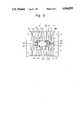
- FIG. 3illustrates a semiconductor device 11 according to the present invention.
- reference numeral 12denotes a plastic body, 13 a stage, 14 a semiconductor chip, 15 a plurality of leads, 16 wires, and 20 electrodes of the semiconductor chip 14.
- the leads 15overlap the stage 13, as well as the semiconductor chip 14, so that the leads 15 have enough depth in the plastic body 12 to give them a high pull out resistance and so that a wide region above the semiconductor chip 14 can be used for extending each of the leads 15 to near a desired electrode 20 of the semiconductor chip 14 irrespective of the size of the semiconductor chip 14, i.e., even if it is a size close to the width of the plastic body 12.
- the distance between the leads 15 and the electrodes 20 of the semiconductor chip 14can be decreased to a minimum so that the expensive wires 16 of, e.g., gold can be shortened and the time period for wire bonding can be greatly shortened, resulting in a reduction of production costs.
- FIG. 4aillustrates a lead frame according to the present invention.
- a lead frame 21is made from a metal ribbon of, e.g., 42-alloy by stamping, etching, etc. and contains several parts, each of which is used for fabricating one semiconductor device. Below, a part of a lead frame from which one semiconductor device is fabricated is described.
- the lead frame 21comprises cradles 17 running along the two longitudinal sides of the lead frame itself and provided with alignment holes, a plurality of leads 15 consisting of an inner lead portion 15a and an outer lead portion 15b, dam bars 18 tying the leads 15 to each other and to the cradles 17, and a receiving portion 22 near the cradles 17 for fixing a tab.
- the lead frame 21does not include a stage on which the semiconductor chip 14 is mounted since both the leads 15 and a stage cannot be formed from a single metal ribbon due to the overlapping thereof in a semiconductor device according to the present invention.
- FIGS. 4b and 4cillustrate a tab 23 comprising a stage 13 and two arms 24.
- the arms 24are bent to differentiate the levels of the stage 13 and the ends of the arms 24.
- a semiconductor chip 14 having electrodes 20is bonded onto a stage 13 of a tab 23 with, e.g., silver paste.
- An insulating film 25, e.g., a polyimide or silicone tape, 50 ⁇ m to 200 ⁇ m thickis bonded onto all of the top surface of the semiconductor chip 14 except for the electrodes 20.
- the insulating film 25is preferably heat resistant since it will be subjected to heat in later processes. This insulating film 25 may serve not only as an electrical insulating layer but also as a protective layer for a semiconductor chip against damages resulted from direct contacts of leads during wire bonding process.
- the tab 23 on which the chip 14 is mountedis fixed to a lead frame 21 by welding or bonding the arms 24 of the tab 23 and the tab-receiving portions 22 of the lead frame 21.
- the type of weldingis preferably spot welding or heat pressure welding.
- An adhesivesuch as polyimide may be used as a bond.
- the electrodes 20 of the semiconductor chip 14 and the inner lead portions 15a of the leads 15are then interconnected by means of, e.g., gold wire bonding.
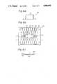
- FIG. 5The thus-assembled and interconnected structure is illustrated in FIG. 5.
- the ends of some inner lead portions 15aoverlap the stage 13 and the semiconductor chip 14.
- the semiconductor chip 14has electrodes 20 arranged along two sides thereof and making a row perpendicular to the row of the leads 15, all of the ends of the inner lead portions 15a extend to near the electrodes 20 of the chip 14 since the leads 15 can occupy the region above the chip 14. This possibility of an unrestricted layout of the inner lead portions is a great advantage of the present invention.
- the thus-assembled and interconnected structurecomprising the lead frame 21, the tab 23, the chip 14, and the wires 16 is set in an transfer mold comprising on upper half and a lower half.
- the moldhas a mold space having peripheries along the dam bars 18 and near the cradles 17 so that a structure consisting of the stage 13, the chip 14, the inner lead portions 15a of the leads 15, and the wires 16 can be molded in plastic, e.g., epoxy resin.
- plastice.g., epoxy resin.
- a semiconductor device having a molded plastic body 6.6 mm widecan contain a semiconductor chip 5.5 mm wide and can have a high resistance to withdrawal of the leads.
- a prior art semiconductor device having a molded plastic body 6.6 mm widecan contain only a semiconductor chip 4 mm wide at the maximum since the depth of the inner leads and the space between the inner leads and the stage must be at least 1 mm and 0.3 mm, respectively.
- FIGS. 6a, 6b, and 6cillustrate another embodiment of the present invention in which a stage on which a semiconductor chip is mounted is a capacitor.
- a capacitor 40is made of a ceramic plate 41 of, e.g., alumina provided with electrodes 42.
- the capacitor 40is fixed to a lead frame 43 at the point indicated by the broken lines in FIG. 6b after a semiconductor chip 14 is mounted onto the capacitor 40.
- the lead frame 43may have receiving portions 44 which do not overlap the inner lead portions of the leads.
- the capacitor 40may be directly fixed to the lead frame 43.
- the capacitor itselfis proposed as a stage for improving the characteristics of a semiconductor chip mounted on the stage.
- An armless metal stagemay be used in combination with a lead frame similar to that of FIG. 6b.
- FIGS. 7a and 7billustrate a further embodiment of the present invention in which two lead frames are used for fabricating a semiconductor device.
- a stage 13is formed as a part of a first lead frame 50 and is tied to cradles 17 with pinch bars 19.
- a second lead frame 51is similar to the lead frame 21 in FIG. 4a except that the tab-receiving portions are removed.
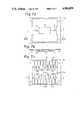
- FIGS. 8a and 8billustrate a cross-sectional and a longitudinal sectional view, respectively, of such a particular mold including an assembly of two lead frames and a semiconductor chip.
- a mold 52comprising an upper half 52a and an lower half 52b holds a single lead frame of the second lead frame 51 at the dam bars 18 thereof and has apertures for receiving the laminations of two cradles.
- a mold space 53contains the assembly of a stage, a chip, and inner lead portions of leads and is connected by a gate 54 to a runner 55 which is connected to a cull (not shown), from where transfer plastic material is fed into the mold space 53.
- FIG. 9illustrates still another embodiment of the present invention in which an insulating layer is inserted between the semiconductor chip and a part of the leads, but not on or above the entire surface of the semiconductor chip except for the electrodes.
- insulating films 62are inserted between the semiconductor chip 14 and the end portions of the lead 15 (15a). This insertion of the insulating film may be effected by adhering the insulating films 62 to the top surface of the semiconductor chip 14 or to the end portions of the leads 15 (15a). FIG. 9 illustrates the former case. This insulating film can also protect a semiconductor chip 14 from damages resulted from direct contacts of the end portions of leads 15 (15a) when wire bonding is effected.
- FIG. 10illustrates still a further embodiment of the present invention in which inner leads 15a overlap a stage 13 but not a semiconductor chip 14.
- an insulating layer 64is inserted between the inner leads 15a and the stage 13.
Landscapes
- Engineering & Computer Science (AREA)
- Power Engineering (AREA)
- Physics & Mathematics (AREA)
- Condensed Matter Physics & Semiconductors (AREA)
- General Physics & Mathematics (AREA)
- Computer Hardware Design (AREA)
- Microelectronics & Electronic Packaging (AREA)
- Manufacturing & Machinery (AREA)
- Lead Frames For Integrated Circuits (AREA)
- Wire Bonding (AREA)
- Encapsulation Of And Coatings For Semiconductor Or Solid State Devices (AREA)
- Structures Or Materials For Encapsulating Or Coating Semiconductor Devices Or Solid State Devices (AREA)
Abstract
Description
1. Field of the Invention
The present invention relates to a semiconductor device and more specifically to a plastic molded semiconductor device and a method for fabricating the same.
2. Description of the Prior Art
A plastic molded semiconductor device, for example, a plastic molded integrated circuit, is known and is fabricated by assembling and interconnecting a semiconductor chip on a substrate or lead frame and molding the entire structure in plastic, with the exception of the leads, to form the body of the component. In this type of fabrication, a single lead frame made from a metal ribbon and comprising a stage and leads is used, with the result that the leads do not overlap the stage on which the semiconductor chip is mounted.
Although the size of a semiconductor chip tends to be increased, the size of a semiconductor device should be a predetermined size, a row space size, or, preferably, as small as possible so that it can be packed more densely. In a semiconductor device, however, leads must be embedded in plastic in more than a fixed length in order to obtain a required pull out resistance, which limits the maximum size of a stage on which a semiconductor chip is mounted and, therefore, limits the maximum size of a semiconductor chip mounted on the stage if the size of a semiconductor device is predetermined.
Further, recent large-scale integrated circuits tend to have electrodes arranged only on two longitudinally opposed edges of a semiconductor chip. Therefore, it is difficult to form a layout of leads adopted suitable for this arrangement of electrodes, and it is particularly difficult if the width from the outer edge of a plastic body to be molded to near the stage on which a semiconductor chip is mounted is narrow.
An object of the present invention is to provide a plastic molded semiconductor device in which a larger semiconductor chip can be mounted and to form a layout of leads which is less restricted than that of the prior art case.
Another object of the present invention is to provide a method for fabricating such a semiconductor device.
These and other objects, features, and advantages of the present invention are accomplished by providing a semiconductor device having a molded plastic body, the semiconductor device comprising: the molded plastic body; a stage in the molded plastic body; a semiconductor chip having electrodes and being mounted on the stage in the molded plastic body; and a plurality of leads each consisting of an inner lead portion embedded in the molded plastic body and an outer lead portion extending outside of the molded plastic body, at least one of the leads overlapping the stage, and the leads and the electrodes of the semiconductor chip being interconnected.
The leads preferably overlap not only the stage but also the semiconductor chip so as to create a larger area for the inner leads. In this case, an insulating layer, preferably a polyimide or silicone film, may be inserted between the leads and the semiconductor chip except for the electrodes of the semiconductor chip. The insertion of an insulating layer is preferable not only for electrically insulating the semiconductor chip from the wires or leads but also for preventing damages resulted from the direct contact of the inner leads to the surface of the semiconductor chip during the wire bonding process.
The present invention also provides a method for fabricating a semiconductor device, including the steps of: mounting a semiconductor chip having electrodes onto a stage; fixing the stage to a lead frame having a plurality of leads each consisting of an inner lead portion and an outer lead portion in such a manner that at least one of the leads overlaps the stage; interconnecting the electrodes of the semiconductor chip and the inner lead portions of the leads; molding the structure of the stage, the semiconductor chip, and the inner lead portions of the leads in plastic; and separating the thus-molded structure from the rest of the lead frame.
The stage may be fixed to the lead frame by welding, such as spot welding or heat pressure welding, or bonding, e.g., with an adhesive, caulking, or the like.
For fixing the stage to the lead frame, a stage alone, a tab comprising a stage and arms, or another lead frame comprising a stage may be used.
The objects, features, and advantages of the present invention are described with reference to the accompanying drawings.
FIG. 1 is a sectional view of a prior art semiconductor device.
FIG. 2 is a plan view of a prior art assembly of a semiconductor device just before molding is effected.
FIG. 3 is a sectional view of a semiconductor device according to the present invention.
FIG. 4a is a plan view of a lead frame used in combination with a tab, and FIGS. 4b and 4c are a plan view and a sectional view, respectively, of a tab.
FIG. 5 is a plan view of an assembly before molding.
FIG. 6a is a plan view of a capacitor stage, FIG. 6b is a plan view of a lead frame used in combination with the capacitor stage of FIG. 6a, and FIG. 6c is a partial sectional view of the assembly of the capacitor stage, a chip, and the lead frame.
FIG. 7a and FIG. 7b are plan view and sectional view taken along the line VIIA--VIIA in FIG. 7a of a lead frame, and FIG. 7c is also a plan view of a lead frame, the lead frame of FIG. 7a and the lead frame of FIG. 7c being used in combination.
FIGS. 8a and 8b are cross-sectional view of and a longitudinal sectional view of a mold including the assembly of two lead frames and a chip.
FIGS. 9 and 10 are sectional views of further semiconductor devices according to the present invention.
Before describing the present invention, the prior art is described with reference to FIGS. 1 and 2. In FIG. 1, a semiconductor device 1 comprises aplastic body 2, astage 3, asemiconductor chip 4, a plurality ofleads 5, andwires 6. Thestage 3 and theleads 5 consist of a single lead frame made from a metal ribbon by stamping or etching it and, therefore, theleads 5 do not overlap thestage 3. FIG. 2 illustrates an example of patterns of an assembly of a prior art lead frame and a semiconductor chip. In FIG. 2, the same parts as in FIG. 1 are denoted by the same reference numerals.Reference numeral 7 denotes cradles, 8 dam bars, and 9 pinch bars, thecradles 7 and a part ofpinch bars 9 near thecradle 7 and thedam bars 8 except for theleads 5 being removed from a finished semiconductor device.
FIG. 3 illustrates asemiconductor device 11 according to the present invention. In the figure,reference numeral 12 denotes a plastic body, 13 a stage, 14 a semiconductor chip, 15 a plurality of leads, 16 wires, and 20 electrodes of thesemiconductor chip 14. In this device, theleads 15 overlap thestage 13, as well as thesemiconductor chip 14, so that theleads 15 have enough depth in theplastic body 12 to give them a high pull out resistance and so that a wide region above thesemiconductor chip 14 can be used for extending each of theleads 15 to near a desiredelectrode 20 of thesemiconductor chip 14 irrespective of the size of thesemiconductor chip 14, i.e., even if it is a size close to the width of theplastic body 12. Further, in this construction of a semiconductor device, the distance between theleads 15 and theelectrodes 20 of thesemiconductor chip 14 can be decreased to a minimum so that theexpensive wires 16 of, e.g., gold can be shortened and the time period for wire bonding can be greatly shortened, resulting in a reduction of production costs.
FIG. 4a illustrates a lead frame according to the present invention. Alead frame 21 is made from a metal ribbon of, e.g., 42-alloy by stamping, etching, etc. and contains several parts, each of which is used for fabricating one semiconductor device. Below, a part of a lead frame from which one semiconductor device is fabricated is described. Thelead frame 21 comprisescradles 17 running along the two longitudinal sides of the lead frame itself and provided with alignment holes, a plurality ofleads 15 consisting of aninner lead portion 15a and anouter lead portion 15b,dam bars 18 tying theleads 15 to each other and to thecradles 17, and a receivingportion 22 near thecradles 17 for fixing a tab. Thelead frame 21 does not include a stage on which thesemiconductor chip 14 is mounted since both theleads 15 and a stage cannot be formed from a single metal ribbon due to the overlapping thereof in a semiconductor device according to the present invention.
FIGS. 4b and 4c illustrate atab 23 comprising astage 13 and twoarms 24. Thearms 24 are bent to differentiate the levels of thestage 13 and the ends of thearms 24.
In the fabrication of a semiconductor device, referring to FIGS. 3 to 5, asemiconductor chip 14 havingelectrodes 20 is bonded onto astage 13 of atab 23 with, e.g., silver paste. An insulatingfilm 25, e.g., a polyimide or silicone tape, 50 λm to 200 λm thick is bonded onto all of the top surface of thesemiconductor chip 14 except for theelectrodes 20. The insulatingfilm 25 is preferably heat resistant since it will be subjected to heat in later processes. This insulatingfilm 25 may serve not only as an electrical insulating layer but also as a protective layer for a semiconductor chip against damages resulted from direct contacts of leads during wire bonding process. Next, thetab 23 on which thechip 14 is mounted is fixed to alead frame 21 by welding or bonding thearms 24 of thetab 23 and the tab-receivingportions 22 of thelead frame 21. The type of welding is preferably spot welding or heat pressure welding. An adhesive such as polyimide may be used as a bond. Theelectrodes 20 of thesemiconductor chip 14 and theinner lead portions 15a of theleads 15 are then interconnected by means of, e.g., gold wire bonding.
The thus-assembled and interconnected structure is illustrated in FIG. 5. As can be seen from FIG. 5, the ends of someinner lead portions 15a overlap thestage 13 and thesemiconductor chip 14. In FIG. 5, though thesemiconductor chip 14 haselectrodes 20 arranged along two sides thereof and making a row perpendicular to the row of theleads 15, all of the ends of theinner lead portions 15a extend to near theelectrodes 20 of thechip 14 since theleads 15 can occupy the region above thechip 14. This possibility of an unrestricted layout of the inner lead portions is a great advantage of the present invention.
The thus-assembled and interconnected structure comprising thelead frame 21, thetab 23, thechip 14, and thewires 16 is set in an transfer mold comprising on upper half and a lower half. The mold has a mold space having peripheries along the dam bars 18 and near thecradles 17 so that a structure consisting of thestage 13, thechip 14, theinner lead portions 15a of theleads 15, and thewires 16 can be molded in plastic, e.g., epoxy resin. After the molding is carried out, thecradles 17 and the dam bars 18, but not the portions of theleads 15, are removed with a press so as to separate the molded plastic body and theouter lead portions 15b, corresponding to an individual plastic molded semiconductor device. Conventional processes such as metal plating, bending the outer lead, etc. may then be carried out.
In accordance with the present invention, a semiconductor device having a molded plastic body 6.6 mm wide can contain a semiconductor chip 5.5 mm wide and can have a high resistance to withdrawal of the leads. In comparison, a prior art semiconductor device having a molded plastic body 6.6 mm wide can contain only asemiconductor chip 4 mm wide at the maximum since the depth of the inner leads and the space between the inner leads and the stage must be at least 1 mm and 0.3 mm, respectively.
FIGS. 6a, 6b, and 6c illustrate another embodiment of the present invention in which a stage on which a semiconductor chip is mounted is a capacitor. For example, acapacitor 40 is made of aceramic plate 41 of, e.g., alumina provided withelectrodes 42. Thecapacitor 40 is fixed to alead frame 43 at the point indicated by the broken lines in FIG. 6b after asemiconductor chip 14 is mounted onto thecapacitor 40. To fix thecapacitor 40 to thelead frame 43, thelead frame 43 may have receivingportions 44 which do not overlap the inner lead portions of the leads. Thus, thecapacitor 40 may be directly fixed to thelead frame 43. The capacitor itself is proposed as a stage for improving the characteristics of a semiconductor chip mounted on the stage.
An armless metal stage may be used in combination with a lead frame similar to that of FIG. 6b.
FIGS. 7a and 7b illustrate a further embodiment of the present invention in which two lead frames are used for fabricating a semiconductor device. In this embodiment, astage 13 is formed as a part of afirst lead frame 50 and is tied tocradles 17 with pinch bars 19. Asecond lead frame 51 is similar to thelead frame 21 in FIG. 4a except that the tab-receiving portions are removed.
The assembling and interconnecting processes are similar to those in the embodiments described before except that thestage 13 is fixed to thesecond lead frame 51 by fixing the twolead frames cradles 17. In the molding process, a particular mold adopted for receiving two lead frames is necessary. FIGS. 8a and 8b illustrate a cross-sectional and a longitudinal sectional view, respectively, of such a particular mold including an assembly of two lead frames and a semiconductor chip. As can be seen from FIGS. 8a and 8b, amold 52 comprising anupper half 52a and anlower half 52b holds a single lead frame of thesecond lead frame 51 at the dam bars 18 thereof and has apertures for receiving the laminations of two cradles. Amold space 53 contains the assembly of a stage, a chip, and inner lead portions of leads and is connected by agate 54 to arunner 55 which is connected to a cull (not shown), from where transfer plastic material is fed into themold space 53.
FIG. 9 illustrates still another embodiment of the present invention in which an insulating layer is inserted between the semiconductor chip and a part of the leads, but not on or above the entire surface of the semiconductor chip except for the electrodes.
In asemiconductor device 61 in FIG. 9, insulatingfilms 62 are inserted between thesemiconductor chip 14 and the end portions of the lead 15 (15a). This insertion of the insulating film may be effected by adhering the insulatingfilms 62 to the top surface of thesemiconductor chip 14 or to the end portions of the leads 15 (15a). FIG. 9 illustrates the former case. This insulating film can also protect asemiconductor chip 14 from damages resulted from direct contacts of the end portions of leads 15 (15a) when wire bonding is effected.
FIG. 10 illustrates still a further embodiment of the present invention in which inner leads 15a overlap astage 13 but not asemiconductor chip 14. In thissemiconductor device 63, an insulatinglayer 64 is inserted between theinner leads 15a and thestage 13.
Claims (10)
1. A semiconductor device having a molded plastic body, said semiconductor device comprising:
a semiconductor chip having a major surface and having electrodes formed on said major surface, said semiconductor chip being encapsulated in the molded plastic body;
a thin, flat, self-supportive metal stage onto which said semiconductor chip is bonded so that said major surface is opposite to and faces said metal stage, said stage being encapsulated in said molded plastic body;
a plurality of leads, each comprising an inner lead end portion embedded in the molded plastic body and an outer lead end portion extending outside of the molded plastic body, said inner lead end portions of the leads being spaced apart from said semiconductor chips, said inner lead end portion of at least one of the leads overlapping said stage and extending over said major surface of said semiconductor chip; and
interconnection wires interconnecting each of said inner lead end portions and each of said electrodes of said semiconductor chip.
2. A semiconductor device having a molded plastic body, said semiconductor device comprising:
a semiconductor chip having electrodes and being encapsulated in the molded plastic body;
a thin, flat, self-supportive metal stage onto which said semiconductor chip is bonded, said stage being encapsulated in said molded plastic body;
a plurality of leads, each comprising an inner lead end portion embedded in the molded plastic body and an outer lead end portion extending outside of the molded plastic body, said inner lead end portions of the leads being spaced apart from said semiconductor chips, said inner lead end portion of at least one of the leads overlapping said stage and said semiconductor chip; and
interconnection wires interconnecting each of said inner lead end portions and each of said electrodes of said semiconductor chip, wherein said electrodes are arranged along at least one side of said semiconductor chip and said inner lead end portion of at least one of said leads extends over said semiconductor chip to a position adjacent to inner sides of said electrodes relative to said semiconductor chip.
3. A semiconductor device according to claim 2, wherein an insulating film covers an entire top surface of the semiconductor chip except for the electrodes thereof.
4. A semiconductor device according to claim 2, wherein an insulating film exists in part of the space between the semiconductor chip and only the inner lead end portions of the leads.
5. A semiconductor device according to claim 4, wherein the insulating film between the semiconductor chip and the inner lead end portions of the leads is adhered to the end portion of the leads.
6. A semiconductor device according to claim 4, wherein the insulating film between the semiconductor chip and the inner lead end portions of the leads is adhered to the semiconductor chip.
7. A semiconductor device according to claim 3 or 4, wherein the insulating film is of polyimide.
8. A semiconductor device according to claim 3 or 4, wherein the insulating film is silicone.
9. A semiconductor device according to claim 2, wherein the inner lead end portions of the leads are arranged in at least one row, said electrodes of the semiconductor chip being arranged along two sides of the semiconductor chip forming rows of electrodes which run perpendicular to at least one row of leads.
10. A semiconductor device having a molded plastic body, said semiconductor device comprising:
a semiconductor chip having electrodes and being encapsulated in the molded plastic body;
a thin, flat, self-supportive metal stage onto which said semiconductor chip is bonded, said stage being encapsulated in said molded plastic body;
a plurality of leads, each comprising an inner lead end portion embedded in the molded plastic body and an outer lead end portion extending outside of the molded plastic body, said inner lead end portions of the leads being spaced apart from said semiconductor chips, said inner lead end portion of at least one of the leads overlapping said stage and said semiconductor chip; and
interconnection wires interconnecting each of said inner lead end portions and each of said electrodes of said semiconductor chip, wherein the stage is a capacitor made of a ceramic plate having two electrodes, each electrode being interconnected to one of the leads.
Priority Applications (1)
| Application Number | Priority Date | Filing Date | Title |
|---|---|---|---|
| US08/001,613USRE35109E (en) | 1982-10-08 | 1993-01-07 | Semiconductor device and method for fabricating the same |
Applications Claiming Priority (2)
| Application Number | Priority Date | Filing Date | Title |
|---|---|---|---|
| JP57177353AJPS5966157A (en) | 1982-10-08 | 1982-10-08 | Semiconductor device and its manufacturing method |
| JP57-177353 | 1982-10-08 |
Related Child Applications (1)
| Application Number | Title | Priority Date | Filing Date |
|---|---|---|---|
| US08/001,613ReissueUSRE35109E (en) | 1982-10-08 | 1993-01-07 | Semiconductor device and method for fabricating the same |
Publications (1)
| Publication Number | Publication Date |
|---|---|
| US4984059Atrue US4984059A (en) | 1991-01-08 |
Family
ID=16029481
Family Applications (2)
| Application Number | Title | Priority Date | Filing Date |
|---|---|---|---|
| US06/539,781CeasedUS4984059A (en) | 1982-10-08 | 1983-10-07 | Semiconductor device and a method for fabricating the same |
| US08/001,613Expired - LifetimeUSRE35109E (en) | 1982-10-08 | 1993-01-07 | Semiconductor device and method for fabricating the same |
Family Applications After (1)
| Application Number | Title | Priority Date | Filing Date |
|---|---|---|---|
| US08/001,613Expired - LifetimeUSRE35109E (en) | 1982-10-08 | 1993-01-07 | Semiconductor device and method for fabricating the same |
Country Status (7)
| Country | Link |
|---|---|
| US (2) | US4984059A (en) |
| EP (1) | EP0108502B1 (en) |
| JP (1) | JPS5966157A (en) |
| KR (1) | KR860000410B1 (en) |
| CA (1) | CA1217876A (en) |
| DE (1) | DE3379008D1 (en) |
| IE (1) | IE55078B1 (en) |
Cited By (74)
| Publication number | Priority date | Publication date | Assignee | Title |
|---|---|---|---|---|
| US5168345A (en)* | 1990-08-15 | 1992-12-01 | Lsi Logic Corporation | Semiconductor device having a universal die size inner lead layout |
| US5198883A (en)* | 1988-08-06 | 1993-03-30 | Kabushiki Kaisha Toshiba | Semiconductor device having an improved lead arrangement and method for manufacturing the same |
| US5262927A (en)* | 1992-02-07 | 1993-11-16 | Lsi Logic Corporation | Partially-molded, PCB chip carrier package |
| US5291061A (en)* | 1993-04-06 | 1994-03-01 | Micron Semiconductor, Inc. | Multi-chip stacked devices |
| US5299730A (en)* | 1989-08-28 | 1994-04-05 | Lsi Logic Corporation | Method and apparatus for isolation of flux materials in flip-chip manufacturing |
| US5334803A (en)* | 1991-10-30 | 1994-08-02 | Mitsubishi Denki Kabushiki Kaisha | Semiconductor device and method of producing the same |
| US5388327A (en)* | 1993-09-15 | 1995-02-14 | Lsi Logic Corporation | Fabrication of a dissolvable film carrier containing conductive bump contacts for placement on a semiconductor device package |
| US5399903A (en)* | 1990-08-15 | 1995-03-21 | Lsi Logic Corporation | Semiconductor device having an universal die size inner lead layout |
| US5409866A (en)* | 1991-12-27 | 1995-04-25 | Fujitsu Ltd. | Process for manufacturing a semiconductor device affixed to an upper and a lower leadframe |
| US5434750A (en)* | 1992-02-07 | 1995-07-18 | Lsi Logic Corporation | Partially-molded, PCB chip carrier package for certain non-square die shapes |
| US5438477A (en)* | 1993-08-12 | 1995-08-01 | Lsi Logic Corporation | Die-attach technique for flip-chip style mounting of semiconductor dies |
| US5440169A (en)* | 1993-01-08 | 1995-08-08 | Mitsubishi Denki Kabushiki Kaisha | Resin-packaged semiconductor device with flow prevention dimples |
| US5440170A (en)* | 1990-09-10 | 1995-08-08 | Fujitsu Limited | Semiconductor device having a die pad with rounded edges and its manufacturing method |
| USRE35109E (en)* | 1982-10-08 | 1995-12-05 | Fujitsu Limited | Semiconductor device and method for fabricating the same |
| US5585600A (en)* | 1993-09-02 | 1996-12-17 | International Business Machines Corporation | Encapsulated semiconductor chip module and method of forming the same |
| US5596172A (en)* | 1993-05-07 | 1997-01-21 | Motorola, Inc. | Planar encapsulation process |
| US5696029A (en)* | 1993-08-31 | 1997-12-09 | Texas Instruments Incorporated | Process for manufacturing a lead frame |
| US5717246A (en)* | 1996-07-29 | 1998-02-10 | Micron Technology, Inc. | Hybrid frame with lead-lock tape |
| US5734198A (en)* | 1994-11-10 | 1998-03-31 | Micron Technology, Inc. | Multi-layer lead frame for a semiconductor device |
| US5733800A (en)* | 1996-05-21 | 1998-03-31 | Micron Technology, Inc. | Underfill coating for LOC package |
| US5759875A (en)* | 1996-10-04 | 1998-06-02 | Micron Technology, Inc. | Reduced filler particle size encapsulant for reduction in die surface damage in LOC packages and method of use |
| US5770479A (en)* | 1996-01-11 | 1998-06-23 | Micron Technology, Inc. | Bonding support for leads-over-chip process |
| US5834691A (en)* | 1995-01-19 | 1998-11-10 | Sharp Kabushiki Kaisha | Lead frame, its use in the fabrication of resin-encapsulated semiconductor device |
| US5847445A (en)* | 1996-11-04 | 1998-12-08 | Micron Technology, Inc. | Die assemblies using suspended bond wires, carrier substrates and dice having wire suspension structures, and methods of fabricating same |
| US5869355A (en)* | 1996-06-11 | 1999-02-09 | Yamaha Corp. | Lead frame with increased strength and manufacture of semiconductor device |
| US5872398A (en)* | 1996-01-11 | 1999-02-16 | Micron Technology, Inc. | Reduced stress LOC assembly including cantilevered leads |
| US5923081A (en)* | 1997-05-15 | 1999-07-13 | Micron Technology, Inc. | Compression layer on the leadframe to reduce stress defects |
| US5959349A (en)* | 1997-02-25 | 1999-09-28 | Micron Technology, Inc. | Transfer molding encapsulation of a semiconductor die with attached heat sink |
| US5965936A (en)* | 1997-12-31 | 1999-10-12 | Micron Technology, Inc. | Multi-layer lead frame for a semiconductor device |
| US5982018A (en)* | 1997-05-23 | 1999-11-09 | Micron Technology, Inc. | Thin film capacitor coupons for memory modules and multi-chip modules |
| US6005286A (en)* | 1997-10-06 | 1999-12-21 | Micron Technology, Inc. | Increasing the gap between a lead frame and a semiconductor die |
| US6046506A (en)* | 1997-03-24 | 2000-04-04 | Rohm Co., Ltd. | Semiconductor device with package |
| US6054754A (en)* | 1997-06-06 | 2000-04-25 | Micron Technology, Inc. | Multi-capacitance lead frame decoupling device |
| US6072228A (en)* | 1996-10-25 | 2000-06-06 | Micron Technology, Inc. | Multi-part lead frame with dissimilar materials and method of manufacturing |
| GB2344934A (en)* | 1995-10-24 | 2000-06-21 | Altera Corp | Integrated circuit package |
| US6114756A (en)* | 1998-04-01 | 2000-09-05 | Micron Technology, Inc. | Interdigitated capacitor design for integrated circuit leadframes |
| US6117797A (en)* | 1998-09-03 | 2000-09-12 | Micron Technology, Inc. | Attachment method for heat sinks and devices involving removal of misplaced encapsulant |
| US6124150A (en)* | 1998-08-20 | 2000-09-26 | Micron Technology, Inc. | Transverse hybrid LOC package |
| US6194779B1 (en)* | 1989-11-28 | 2001-02-27 | Kabushiki Kaisha Toshiba | Plastic mold type semiconductor device |
| US6215176B1 (en)* | 1999-05-04 | 2001-04-10 | Sitron Precision Co., Ltd. | Dual leadframe package |
| US6277225B1 (en) | 1996-03-13 | 2001-08-21 | Micron Technology, Inc. | Stress reduction feature for LOC lead frame |
| US6297960B1 (en) | 1998-06-30 | 2001-10-02 | Micron Technology, Inc. | Heat sink with alignment and retaining features |
| US6297548B1 (en) | 1998-06-30 | 2001-10-02 | Micron Technology, Inc. | Stackable ceramic FBGA for high thermal applications |
| US6384333B1 (en) | 1996-05-21 | 2002-05-07 | Micron Technology, Inc. | Underfill coating for LOC package |
| US6444501B1 (en) | 2001-06-12 | 2002-09-03 | Micron Technology, Inc. | Two stage transfer molding method to encapsulate MMC module |
| US6472737B1 (en) | 1998-01-20 | 2002-10-29 | Micron Technology, Inc. | Lead frame decoupling capacitor, semiconductor device packages including the same and methods |
| US20020186549A1 (en)* | 2001-06-11 | 2002-12-12 | Bolken Todd O. | Alternative method used to package multi media card by transfer molding |
| US6586821B1 (en) | 1997-06-23 | 2003-07-01 | Stmicroelectronics, Inc. | Lead-frame forming for improved thermal performance |
| US20030151120A1 (en)* | 2000-06-28 | 2003-08-14 | Hundt Michael J. | Lead-frame forming for improved thermal performance |
| US20040109525A1 (en)* | 2002-12-09 | 2004-06-10 | Chieng Koc Vai Chieng Aka Michael | Automatic chip counting system (process) |
| US6791842B2 (en)* | 2002-11-12 | 2004-09-14 | Kingpak Technology Inc. | Image sensor structure |
| US20050062139A1 (en)* | 2003-09-24 | 2005-03-24 | Chung-Hsing Tzu | Reinforced die pad support structure |
| US20050082681A1 (en)* | 2001-11-23 | 2005-04-21 | Jacob Wijdenes | Semiconductor device and method of enveloping an intergrated circuit |
| US20070170859A1 (en)* | 2006-01-25 | 2007-07-26 | Dong Soo Choi | Organic light emitting display and method of fabricating the same |
| US20070170845A1 (en)* | 2006-01-26 | 2007-07-26 | Dong Soo Choi | Organic light emitting display device |
| US20070170860A1 (en)* | 2006-01-25 | 2007-07-26 | Dong Soo Choi | Organic light-emitting display device with frit seal and reinforcing structure bonded to frame |
| US20070173167A1 (en)* | 2006-01-26 | 2007-07-26 | Young Seo Choi | Organic light-emitting display device and method of fabricating the same |
| US20070170324A1 (en)* | 2006-01-25 | 2007-07-26 | Jae Sun Lee | Organic light emitting display and fabricating method of the same |
| US20070170857A1 (en)* | 2006-01-25 | 2007-07-26 | Dong Soo Choi | Organic light-emitting display device and method of manufacturing the same |
| US20070170839A1 (en)* | 2006-01-20 | 2007-07-26 | Choi Dong S | Organic light-emitting display device with frit seal and reinforcing structure |
| US20070170423A1 (en)* | 2006-01-24 | 2007-07-26 | Choi Dong S | Organic light-emitting display and method of making the same |
| US20070170850A1 (en)* | 2006-01-23 | 2007-07-26 | Choi Dong-Soo | Organic light emitting display and method of fabricating the same |
| US20070170855A1 (en)* | 2006-01-25 | 2007-07-26 | Choi Dong-Soo | Organic light emitting display device and method of fabricating the same |
| US20070176549A1 (en)* | 2006-01-27 | 2007-08-02 | Jin Woo Park | Organic light emitting display and method of fabricating the same |
| US20070177069A1 (en)* | 2006-01-27 | 2007-08-02 | Jong Woo Lee | Organic light emitting display and fabricating method of the same |
| USRE40061E1 (en) | 1993-04-06 | 2008-02-12 | Micron Technology, Inc. | Multi-chip stacked devices |
| US20090267171A1 (en)* | 2008-04-24 | 2009-10-29 | Micron Technology, Inc. | Pre-encapsulated cavity interposer |
| US7834550B2 (en) | 2006-01-24 | 2010-11-16 | Samsung Mobile Display Co., Ltd. | Organic light emitting display and fabricating method of the same |
| US7837530B2 (en) | 2006-03-29 | 2010-11-23 | Samsung Mobile Display Co., Ltd. | Method of sealing an organic light emitting display by means of a glass frit seal assembly |
| US8038495B2 (en) | 2006-01-20 | 2011-10-18 | Samsung Mobile Display Co., Ltd. | Organic light-emitting display device and manufacturing method of the same |
| US8299705B2 (en) | 2006-01-26 | 2012-10-30 | Samsung Display Co., Ltd. | Organic light emitting display device and manufacturing method thereof |
| US11036269B2 (en)* | 2014-09-02 | 2021-06-15 | Delta Electronics (Shanghai) Co., Ltd. | Power module and manufacturing method thereof |
| US11437910B2 (en) | 2014-09-02 | 2022-09-06 | Delta Electronics, Inc. | Power module |
| US12253893B2 (en) | 2014-09-02 | 2025-03-18 | Delta Electronics, Inc. | Power supply apparatus |
Families Citing this family (15)
| Publication number | Priority date | Publication date | Assignee | Title |
|---|---|---|---|---|
| JPS61230344A (en)* | 1985-04-05 | 1986-10-14 | Toray Silicone Co Ltd | Resin-sealed semiconductor device |
| JPS6344750A (en)* | 1986-08-12 | 1988-02-25 | Shinko Electric Ind Co Ltd | Manufacture of resin-sealed type semiconductor device and lead frame for semiconductor device |
| JPS63213347A (en)* | 1987-02-27 | 1988-09-06 | Mitsubishi Electric Corp | semiconductor equipment |
| JPH0724275B2 (en)* | 1987-11-06 | 1995-03-15 | 三菱電機株式会社 | Semiconductor device |
| JP2706077B2 (en)* | 1988-02-12 | 1998-01-28 | 株式会社日立製作所 | Resin-sealed semiconductor device and method of manufacturing the same |
| JPH0215663A (en)* | 1988-07-04 | 1990-01-19 | Tomoegawa Paper Co Ltd | Double-sided adhesive tape for lead frames |
| JPH0650749B2 (en)* | 1989-06-28 | 1994-06-29 | 株式会社東芝 | Semiconductor device and manufacturing method thereof |
| KR920018907A (en)* | 1991-03-23 | 1992-10-22 | 김광호 | Semiconductor leadframe |
| JP3088193B2 (en)* | 1992-06-05 | 2000-09-18 | 三菱電機株式会社 | Method for manufacturing semiconductor device having LOC structure and lead frame used therein |
| JP2866572B2 (en)* | 1994-02-07 | 1999-03-08 | 三菱電機株式会社 | Semiconductor manufacturing method |
| TW314650B (en)* | 1995-06-21 | 1997-09-01 | Oki Electric Ind Co Ltd | |
| US5907769A (en)* | 1996-12-30 | 1999-05-25 | Micron Technology, Inc. | Leads under chip in conventional IC package |
| JP2003017645A (en)* | 2001-07-03 | 2003-01-17 | Shinko Electric Ind Co Ltd | Lead frame and method of fabricating the same |
| US8116102B2 (en)* | 2007-12-26 | 2012-02-14 | Infineon Technologies Ag | Integrated circuit device and method of producing |
| US8946876B2 (en)* | 2011-09-29 | 2015-02-03 | Sharp Kabushiki Kaisha | Semiconductor device |
Citations (10)
| Publication number | Priority date | Publication date | Assignee | Title |
|---|---|---|---|---|
| JPS5240062A (en)* | 1975-09-26 | 1977-03-28 | Hitachi Ltd | Process for production of semiconductor devices |
| US4024570A (en)* | 1974-09-17 | 1977-05-17 | Siemens Aktiengesellschaft | Simplified housing structure including a heat sink for a semiconductor unit |
| JPS5413776A (en)* | 1977-07-01 | 1979-02-01 | Nec Corp | Semiconductor devices |
| GB2036428A (en)* | 1978-11-20 | 1980-06-25 | Hitachi Ltd | A Semiconductor Device |
| JPS55113339A (en)* | 1979-02-22 | 1980-09-01 | Chiyou Lsi Gijutsu Kenkyu Kumiai | Semiconductor integrated circuit device |
| JPS55140249A (en)* | 1979-04-18 | 1980-11-01 | Fujitsu Ltd | Semiconductor device |
| JPS5848952A (en)* | 1981-09-18 | 1983-03-23 | Sumitomo Electric Ind Ltd | Lead frame for integrated circuit |
| EP0089044A2 (en)* | 1982-03-16 | 1983-09-21 | Nec Corporation | A semiconductor device having a container sealed with a solder of low melting point |
| US4527185A (en)* | 1981-01-12 | 1985-07-02 | Avx Corporation | Integrated circuit device and subassembly |
| US4541003A (en)* | 1978-12-27 | 1985-09-10 | Hitachi, Ltd. | Semiconductor device including an alpha-particle shield |
Family Cites Families (10)
| Publication number | Priority date | Publication date | Assignee | Title |
|---|---|---|---|---|
| NL7104239A (en)* | 1970-04-16 | 1971-10-19 | ||
| US3838984A (en)* | 1973-04-16 | 1974-10-01 | Sperry Rand Corp | Flexible carrier and interconnect for uncased ic chips |
| US3922712A (en)* | 1974-05-01 | 1975-11-25 | Gen Motors Corp | Plastic power semiconductor flip chip package |
| JPS522282A (en)* | 1975-06-24 | 1977-01-08 | Hitachi Ltd | Semiconductor device |
| JPS522281A (en)* | 1975-06-24 | 1977-01-08 | Hitachi Ltd | Method of making semiconductor devices |
| US4215360A (en)* | 1978-11-09 | 1980-07-29 | General Motors Corporation | Power semiconductor device assembly having a lead frame with interlock members |
| US4308339A (en)* | 1980-02-07 | 1981-12-29 | Westinghouse Electric Corp. | Method for manufacturing tape including lead frames |
| GB2091035B (en)* | 1981-01-12 | 1985-01-09 | Avx Corp | Integrated circuit device and sub-assembly |
| JPS5966157A (en)* | 1982-10-08 | 1984-04-14 | Fujitsu Ltd | Semiconductor device and its manufacturing method |
| JP3595558B2 (en)* | 1991-08-09 | 2004-12-02 | キヤノン株式会社 | Camera and automatic focusing device |
- 1982
- 1982-10-08JPJP57177353Apatent/JPS5966157A/enactiveGranted
- 1983
- 1983-10-04CACA000438288Apatent/CA1217876A/ennot_activeExpired
- 1983-10-06DEDE8383306055Tpatent/DE3379008D1/ennot_activeExpired
- 1983-10-06EPEP83306055Apatent/EP0108502B1/ennot_activeExpired
- 1983-10-07KRKR1019830004765Apatent/KR860000410B1/ennot_activeExpired
- 1983-10-07IEIE2368/83Apatent/IE55078B1/ennot_activeIP Right Cessation
- 1983-10-07USUS06/539,781patent/US4984059A/ennot_activeCeased
- 1993
- 1993-01-07USUS08/001,613patent/USRE35109E/ennot_activeExpired - Lifetime
Patent Citations (10)
| Publication number | Priority date | Publication date | Assignee | Title |
|---|---|---|---|---|
| US4024570A (en)* | 1974-09-17 | 1977-05-17 | Siemens Aktiengesellschaft | Simplified housing structure including a heat sink for a semiconductor unit |
| JPS5240062A (en)* | 1975-09-26 | 1977-03-28 | Hitachi Ltd | Process for production of semiconductor devices |
| JPS5413776A (en)* | 1977-07-01 | 1979-02-01 | Nec Corp | Semiconductor devices |
| GB2036428A (en)* | 1978-11-20 | 1980-06-25 | Hitachi Ltd | A Semiconductor Device |
| US4541003A (en)* | 1978-12-27 | 1985-09-10 | Hitachi, Ltd. | Semiconductor device including an alpha-particle shield |
| JPS55113339A (en)* | 1979-02-22 | 1980-09-01 | Chiyou Lsi Gijutsu Kenkyu Kumiai | Semiconductor integrated circuit device |
| JPS55140249A (en)* | 1979-04-18 | 1980-11-01 | Fujitsu Ltd | Semiconductor device |
| US4527185A (en)* | 1981-01-12 | 1985-07-02 | Avx Corporation | Integrated circuit device and subassembly |
| JPS5848952A (en)* | 1981-09-18 | 1983-03-23 | Sumitomo Electric Ind Ltd | Lead frame for integrated circuit |
| EP0089044A2 (en)* | 1982-03-16 | 1983-09-21 | Nec Corporation | A semiconductor device having a container sealed with a solder of low melting point |
Cited By (200)
| Publication number | Priority date | Publication date | Assignee | Title |
|---|---|---|---|---|
| USRE35109E (en)* | 1982-10-08 | 1995-12-05 | Fujitsu Limited | Semiconductor device and method for fabricating the same |
| US5198883A (en)* | 1988-08-06 | 1993-03-30 | Kabushiki Kaisha Toshiba | Semiconductor device having an improved lead arrangement and method for manufacturing the same |
| US5299730A (en)* | 1989-08-28 | 1994-04-05 | Lsi Logic Corporation | Method and apparatus for isolation of flux materials in flip-chip manufacturing |
| US6194779B1 (en)* | 1989-11-28 | 2001-02-27 | Kabushiki Kaisha Toshiba | Plastic mold type semiconductor device |
| US5399903A (en)* | 1990-08-15 | 1995-03-21 | Lsi Logic Corporation | Semiconductor device having an universal die size inner lead layout |
| US5168345A (en)* | 1990-08-15 | 1992-12-01 | Lsi Logic Corporation | Semiconductor device having a universal die size inner lead layout |
| US5440170A (en)* | 1990-09-10 | 1995-08-08 | Fujitsu Limited | Semiconductor device having a die pad with rounded edges and its manufacturing method |
| US5334803A (en)* | 1991-10-30 | 1994-08-02 | Mitsubishi Denki Kabushiki Kaisha | Semiconductor device and method of producing the same |
| USRE35496E (en)* | 1991-10-30 | 1997-04-29 | Mitsubishi Denki Kabushiki Kaisha | Semiconductor device and method of producing the same |
| US5409866A (en)* | 1991-12-27 | 1995-04-25 | Fujitsu Ltd. | Process for manufacturing a semiconductor device affixed to an upper and a lower leadframe |
| EP0987758A3 (en)* | 1991-12-27 | 2000-05-24 | Fujitsu Limited | Semiconducter device and method of producing the same |
| US5637915A (en)* | 1991-12-27 | 1997-06-10 | Fujitsu Ltd. | Semiconductor device affixed to an upper and a lower leadframe |
| US5434750A (en)* | 1992-02-07 | 1995-07-18 | Lsi Logic Corporation | Partially-molded, PCB chip carrier package for certain non-square die shapes |
| US5262927A (en)* | 1992-02-07 | 1993-11-16 | Lsi Logic Corporation | Partially-molded, PCB chip carrier package |
| US5440169A (en)* | 1993-01-08 | 1995-08-08 | Mitsubishi Denki Kabushiki Kaisha | Resin-packaged semiconductor device with flow prevention dimples |
| USRE36613E (en)* | 1993-04-06 | 2000-03-14 | Micron Technology, Inc. | Multi-chip stacked devices |
| US5291061A (en)* | 1993-04-06 | 1994-03-01 | Micron Semiconductor, Inc. | Multi-chip stacked devices |
| USRE40061E1 (en) | 1993-04-06 | 2008-02-12 | Micron Technology, Inc. | Multi-chip stacked devices |
| US5596172A (en)* | 1993-05-07 | 1997-01-21 | Motorola, Inc. | Planar encapsulation process |
| US5438477A (en)* | 1993-08-12 | 1995-08-01 | Lsi Logic Corporation | Die-attach technique for flip-chip style mounting of semiconductor dies |
| US5696029A (en)* | 1993-08-31 | 1997-12-09 | Texas Instruments Incorporated | Process for manufacturing a lead frame |
| US5585600A (en)* | 1993-09-02 | 1996-12-17 | International Business Machines Corporation | Encapsulated semiconductor chip module and method of forming the same |
| US5388327A (en)* | 1993-09-15 | 1995-02-14 | Lsi Logic Corporation | Fabrication of a dissolvable film carrier containing conductive bump contacts for placement on a semiconductor device package |
| US6124630A (en)* | 1994-11-10 | 2000-09-26 | Micron Technology, Inc. | Multi-layer lead frame for a semiconductor device |
| US6307255B1 (en) | 1994-11-10 | 2001-10-23 | Micron Technology, Inc. | Multi-layer lead frame for a semiconductor device |
| US5734198A (en)* | 1994-11-10 | 1998-03-31 | Micron Technology, Inc. | Multi-layer lead frame for a semiconductor device |
| US5834691A (en)* | 1995-01-19 | 1998-11-10 | Sharp Kabushiki Kaisha | Lead frame, its use in the fabrication of resin-encapsulated semiconductor device |
| GB2344934A (en)* | 1995-10-24 | 2000-06-21 | Altera Corp | Integrated circuit package |
| US6590277B1 (en) | 1996-01-11 | 2003-07-08 | Micron Technology, Inc. | Reduced stress LOC assembly |
| US6083777A (en)* | 1996-01-11 | 2000-07-04 | Micron Technology, Inc. | Reduced stress LOC assembly |
| US6294824B1 (en) | 1996-01-11 | 2001-09-25 | Micron Technology, Inc. | Bonding support for leads-over-chip process |
| US5872398A (en)* | 1996-01-11 | 1999-02-16 | Micron Technology, Inc. | Reduced stress LOC assembly including cantilevered leads |
| US5770479A (en)* | 1996-01-11 | 1998-06-23 | Micron Technology, Inc. | Bonding support for leads-over-chip process |
| US6063650A (en)* | 1996-01-11 | 2000-05-16 | Micron Technology, Inc. | Reduced stress LOC assembly |
| US6277225B1 (en) | 1996-03-13 | 2001-08-21 | Micron Technology, Inc. | Stress reduction feature for LOC lead frame |
| US7112252B2 (en) | 1996-03-13 | 2006-09-26 | Micron Technology, Inc. | Assembly method for semiconductor die and lead frame |
| US6610162B1 (en) | 1996-03-13 | 2003-08-26 | Micron Technology, Inc. | Methods for stress reduction feature for LOC lead frame |
| US6635954B2 (en) | 1996-03-13 | 2003-10-21 | Micron Technology, Inc. | Stress reduction feature for LOC lead frame |
| US20070000599A1 (en)* | 1996-03-13 | 2007-01-04 | Kinsman Larry D | Assembly method for semiconductor die and lead frame |
| US6396131B1 (en) | 1996-03-13 | 2002-05-28 | Micron Technology, Inc. | Stress reduction feature for LOC lead frame |
| US20040056336A1 (en)* | 1996-03-13 | 2004-03-25 | Kinsman Larry D. | Methods for stress reduction feature for LOC lead frame |
| US6090644A (en)* | 1996-05-21 | 2000-07-18 | Micron Technology, Inc. | Underfill coating for LOC package |
| US6384333B1 (en) | 1996-05-21 | 2002-05-07 | Micron Technology, Inc. | Underfill coating for LOC package |
| US6538200B2 (en) | 1996-05-21 | 2003-03-25 | Micron Technology, Inc. | Underfill coating for LOC package |
| US5960258A (en)* | 1996-05-21 | 1999-09-28 | Micron Technology, Inc. | Underfill coating for LOC package |
| US6114627A (en)* | 1996-05-21 | 2000-09-05 | Micron Technology, Inc. | Underfill coating for LOC package |
| US6297546B1 (en) | 1996-05-21 | 2001-10-02 | Micron Technology, Inc. | Underfill coating for LOC package |
| US6670550B2 (en) | 1996-05-21 | 2003-12-30 | Micron Technology, Inc. | Underfill coating for LOC package |
| US5733800A (en)* | 1996-05-21 | 1998-03-31 | Micron Technology, Inc. | Underfill coating for LOC package |
| US6310288B1 (en) | 1996-05-21 | 2001-10-30 | Micron Technology, Inc. | Underfill coating for loc package |
| US5869355A (en)* | 1996-06-11 | 1999-02-09 | Yamaha Corp. | Lead frame with increased strength and manufacture of semiconductor device |
| US6545343B2 (en) | 1996-07-29 | 2003-04-08 | Micron Technology, Inc. | Hybrid frame with lead-lock tape |
| US6737734B2 (en) | 1996-07-29 | 2004-05-18 | Micron Technology, Inc. | Structure and method for securing bussing leads |
| US6146922A (en)* | 1996-07-29 | 2000-11-14 | Micron Technology, Inc. | Hybrid frame with lead-lock tape |
| US6008531A (en)* | 1996-07-29 | 1999-12-28 | Micron Technology, Inc. | Hybrid frame with lead-lock tape |
| US5717246A (en)* | 1996-07-29 | 1998-02-10 | Micron Technology, Inc. | Hybrid frame with lead-lock tape |
| US6251708B1 (en) | 1996-07-29 | 2001-06-26 | Micron Technology, Inc. | Hybrid frame with lead-lock tape |
| US5897340A (en)* | 1996-07-29 | 1999-04-27 | Micron Technology, Inc. | Hybrid frame with lead-lock tape |
| US6707136B2 (en) | 1996-09-04 | 2004-03-16 | Micron Technology, Inc. | Multi-layer lead frame for a semiconductor device |
| US6515353B2 (en) | 1996-09-04 | 2003-02-04 | Micron Technology, Inc. | Multi-layer lead frame for a semiconductor device |
| US5759875A (en)* | 1996-10-04 | 1998-06-02 | Micron Technology, Inc. | Reduced filler particle size encapsulant for reduction in die surface damage in LOC packages and method of use |
| US20070057353A1 (en)* | 1996-10-25 | 2007-03-15 | Hinkle S D | Multi-part lead frame with dissimilar materials |
| US6140154A (en)* | 1996-10-25 | 2000-10-31 | Micron Technology, Inc. | Multi-part lead frame with dissimilar materials and method of manufacturing |
| US20020076857A1 (en)* | 1996-10-25 | 2002-06-20 | Hinkle S. Derek | Multi-part lead frame with dissimilar materials and method of manufacturing |
| US7321160B2 (en) | 1996-10-25 | 2008-01-22 | Micron Technology, Inc. | Multi-part lead frame |
| US20050224928A1 (en)* | 1996-10-25 | 2005-10-13 | Hinkle S D | Multi-part lead frame with dissimilar materials |
| US6946722B2 (en) | 1996-10-25 | 2005-09-20 | Micron Technology, Inc. | Multi-part lead frame with dissimilar materials |
| US20060125065A1 (en)* | 1996-10-25 | 2006-06-15 | Hinkle S D | Multi-part lead frame with dissimilar materials |
| US6362022B1 (en) | 1996-10-25 | 2002-03-26 | Micron Technology, Inc. | Multi-part lead frame with dissimilar materials and method of manufacturing |
| US20050146002A1 (en)* | 1996-10-25 | 2005-07-07 | Hinkle S. D. | Multi-part lead frame with dissimilar materials |
| US6902952B2 (en) | 1996-10-25 | 2005-06-07 | Micron Technology, Inc. | Multi-part lead frame with dissimilar materials and method of manufacturing |
| US6072228A (en)* | 1996-10-25 | 2000-06-06 | Micron Technology, Inc. | Multi-part lead frame with dissimilar materials and method of manufacturing |
| US5847445A (en)* | 1996-11-04 | 1998-12-08 | Micron Technology, Inc. | Die assemblies using suspended bond wires, carrier substrates and dice having wire suspension structures, and methods of fabricating same |
| US20040033644A1 (en)* | 1997-02-25 | 2004-02-19 | Wensel Richard W. | Methods for transfer molding encapsulation of a semiconductor die with attached heat sink |
| US7061082B2 (en) | 1997-02-25 | 2006-06-13 | Micron Technology, Inc. | Semiconductor die with attached heat sink and transfer mold |
| US20040004274A1 (en)* | 1997-02-25 | 2004-01-08 | Wensel Richard W. | Semiconductor die with attached heat sink and transfer mold |
| US6583504B2 (en) | 1997-02-25 | 2003-06-24 | Micron Technology, Inc. | Semiconductor die with attached heat sink and transfer mold |
| US6373132B2 (en) | 1997-02-25 | 2002-04-16 | Micron Technology, Inc. | Semiconductor die with attached heat sink and transfer mold |
| US5959349A (en)* | 1997-02-25 | 1999-09-28 | Micron Technology, Inc. | Transfer molding encapsulation of a semiconductor die with attached heat sink |
| US6001672A (en)* | 1997-02-25 | 1999-12-14 | Micron Technology, Inc. | Method for transfer molding encapsulation of a semiconductor die with attached heat sink |
| US6869811B2 (en) | 1997-02-25 | 2005-03-22 | Micron Technology, Inc. | Methods for transfer molding encapsulation of a semiconductor die with attached heat sink |
| US6403387B1 (en) | 1997-02-25 | 2002-06-11 | Micron Technology | Method and apparatus for transfer molding encapsulation of a semiconductor die with attached heat sink |
| US6249050B1 (en) | 1997-02-25 | 2001-06-19 | Micron Technology, Inc. | Encapsulated transfer molding of a semiconductor die with attached heat sink |
| US20020076856A1 (en)* | 1997-02-25 | 2002-06-20 | Wensel Richard W. | Method and apparatus for transfer molding encapsulation of a semiconductor die with attached heat sink |
| US6046506A (en)* | 1997-03-24 | 2000-04-04 | Rohm Co., Ltd. | Semiconductor device with package |
| US6657288B2 (en) | 1997-05-15 | 2003-12-02 | Micron Technology, Inc. | Compression layer on the lead frame to reduce stress defects |
| US6140695A (en)* | 1997-05-15 | 2000-10-31 | Micron Technology, Inc. | Compression layer on the leadframe to reduce stress defects |
| US6221695B1 (en) | 1997-05-15 | 2001-04-24 | Micron Technology, Inc. | Method for fabricating a compression layer on the dead frame to reduce stress defects |
| US5923081A (en)* | 1997-05-15 | 1999-07-13 | Micron Technology, Inc. | Compression layer on the leadframe to reduce stress defects |
| US6486539B1 (en) | 1997-05-15 | 2002-11-26 | Micron Technology, Inc. | Compression layer on the leadframe to reduce stress defects |
| US6342724B1 (en) | 1997-05-23 | 2002-01-29 | Micron Technology, Inc. | Thin film capacitor coupons for memory modules and multi-chip modules |
| US6165814A (en)* | 1997-05-23 | 2000-12-26 | Micron Technology, Inc. | Thin film capacitor coupons for memory modules and multi-chip modules |
| US5982018A (en)* | 1997-05-23 | 1999-11-09 | Micron Technology, Inc. | Thin film capacitor coupons for memory modules and multi-chip modules |
| US6504236B2 (en) | 1997-06-06 | 2003-01-07 | Micron Technology, Inc. | Semiconductor die assembly having leadframe decoupling characters and method |
| US6054754A (en)* | 1997-06-06 | 2000-04-25 | Micron Technology, Inc. | Multi-capacitance lead frame decoupling device |
| US6310388B1 (en) | 1997-06-06 | 2001-10-30 | Micron Technology, Inc. | Semiconductor die assembly having leadframe decoupling characters |
| US6184574B1 (en) | 1997-06-06 | 2001-02-06 | Micron Technology, Inc. | Multi-capacitance lead frame decoupling device |
| US6781219B2 (en) | 1997-06-06 | 2004-08-24 | Micron Technology, Inc. | Semiconductor die assembly having leadframe decoupling characters |
| US6586821B1 (en) | 1997-06-23 | 2003-07-01 | Stmicroelectronics, Inc. | Lead-frame forming for improved thermal performance |
| US6005286A (en)* | 1997-10-06 | 1999-12-21 | Micron Technology, Inc. | Increasing the gap between a lead frame and a semiconductor die |
| US6133068A (en)* | 1997-10-06 | 2000-10-17 | Micron Technology, Inc. | Increasing the gap between a lead frame and a semiconductor die |
| US5965936A (en)* | 1997-12-31 | 1999-10-12 | Micron Technology, Inc. | Multi-layer lead frame for a semiconductor device |
| US20030052402A1 (en)* | 1998-01-20 | 2003-03-20 | Corisis David J. | Lead frame decoupling capacitor, semiconductor device packages including the same and methods |
| US6472737B1 (en) | 1998-01-20 | 2002-10-29 | Micron Technology, Inc. | Lead frame decoupling capacitor, semiconductor device packages including the same and methods |
| US20060118924A1 (en)* | 1998-01-20 | 2006-06-08 | Corisis David J | Lead frame assemblies and decoupling capacitors |
| US6717257B2 (en) | 1998-01-20 | 2004-04-06 | Micron Technology, Inc. | Lead frame decoupling capacitor, semiconductor device packages including the same and methods |
| US6515359B1 (en) | 1998-01-20 | 2003-02-04 | Micron Technology, Inc. | Lead frame decoupling capacitor semiconductor device packages including the same and methods |
| US7071542B2 (en) | 1998-01-20 | 2006-07-04 | Micron Technology, Inc. | Lead frame decoupling capacitor, semiconductor device packages including the same and methods |
| US6531765B2 (en) | 1998-04-01 | 2003-03-11 | Micron Technology, Inc. | Interdigitated capacitor design for integrated circuit lead frames and method |
| US6730994B2 (en) | 1998-04-01 | 2004-05-04 | Micron Technology, Inc. | Interdigitated capacitor design for integrated circuit lead frames and methods |
| US6265764B1 (en) | 1998-04-01 | 2001-07-24 | Micron Technology, Inc. | Interdigitated capacitor design for integrated circuit lead frames |
| US6114756A (en)* | 1998-04-01 | 2000-09-05 | Micron Technology, Inc. | Interdigitated capacitor design for integrated circuit leadframes |
| US6396134B2 (en) | 1998-04-01 | 2002-05-28 | Micron Technology, Inc. | Interdigitated capacitor design for integrated circuit lead frames |
| US20080042252A1 (en)* | 1998-06-30 | 2008-02-21 | Micron Technology, Inc. | Stackable ceramic fbga for high thermal applications |
| US6650007B2 (en) | 1998-06-30 | 2003-11-18 | Micron Technology, Inc. | Stackable ceramic fbga for high thermal applications |
| US6297960B1 (en) | 1998-06-30 | 2001-10-02 | Micron Technology, Inc. | Heat sink with alignment and retaining features |
| US6760224B2 (en) | 1998-06-30 | 2004-07-06 | Micron Technology, Inc. | Heat sink with alignment and retaining features |
| US20050146010A1 (en)* | 1998-06-30 | 2005-07-07 | Moden Walter L. | Stackable ceramic FBGA for high thermal applications |
| US6297548B1 (en) | 1998-06-30 | 2001-10-02 | Micron Technology, Inc. | Stackable ceramic FBGA for high thermal applications |
| US7285442B2 (en) | 1998-06-30 | 2007-10-23 | Micron Technology, Inc. | Stackable ceramic FBGA for high thermal applications |
| US20040104408A1 (en)* | 1998-06-30 | 2004-06-03 | Moden Walter L. | Stackable ceramic FBGA for high thermal applications |
| US7829991B2 (en) | 1998-06-30 | 2010-11-09 | Micron Technology, Inc. | Stackable ceramic FBGA for high thermal applications |
| US6525943B2 (en) | 1998-06-30 | 2003-02-25 | Micron Technology, Inc. | Heat sink with alignment and retaining features |
| US6858926B2 (en) | 1998-06-30 | 2005-02-22 | Micron Technology, Inc. | Stackable ceramic FBGA for high thermal applications |
| US20030162327A1 (en)* | 1998-08-20 | 2003-08-28 | Corisis David J. | Methods for transverse hybrid LOC package |
| US6259153B1 (en) | 1998-08-20 | 2001-07-10 | Micron Technology, Inc. | Transverse hybrid LOC package |
| US6218216B1 (en) | 1998-08-20 | 2001-04-17 | Micron Technology, Inc. | Transverse hybrid LOC package |
| US6753598B2 (en) | 1998-08-20 | 2004-06-22 | Micron Technology, Inc. | Transverse hybrid LOC package |
| US6476468B2 (en) | 1998-08-20 | 2002-11-05 | Micron Technology, Inc. | Transverse hybrid LOC package |
| US6150710A (en)* | 1998-08-20 | 2000-11-21 | Micron Technology, Inc. | Transverse hybrid LOC package |
| US6124150A (en)* | 1998-08-20 | 2000-09-26 | Micron Technology, Inc. | Transverse hybrid LOC package |
| US6406943B2 (en) | 1998-08-20 | 2002-06-18 | Micron Technology, Inc. | Transverse hybrid LOC package |
| US20020195694A1 (en)* | 1998-08-20 | 2002-12-26 | Corisis David J. | Transverse hybrid LOC package |
| US6835604B2 (en) | 1998-08-20 | 2004-12-28 | Micron Technology, Inc. | Methods for transverse hybrid LOC package |
| US6531342B2 (en) | 1998-08-20 | 2003-03-11 | Micron Technology, Inst. | Method for transverse hybrid loc package |
| US20040126931A1 (en)* | 1998-09-03 | 2004-07-01 | Hembree David R. | Chip on board and heat sink attachment methods |
| US6596565B1 (en) | 1998-09-03 | 2003-07-22 | Micron Technology, Inc. | Chip on board and heat sink attachment methods |
| US6229204B1 (en) | 1998-09-03 | 2001-05-08 | Micron Technology, Inc. | Chip on board with heat sink attachment |
| US6432840B1 (en) | 1998-09-03 | 2002-08-13 | Micron Technology, Inc. | Methodology of removing misplaced encapsulant for attachment of heat sinks in a chip on board package |
| US6630371B2 (en) | 1998-09-03 | 2003-10-07 | Micron Technology, Inc. | Chip on board and heat sink attachment methods |
| US6806567B2 (en) | 1998-09-03 | 2004-10-19 | Micron Technology, Inc. | Chip on board with heat sink attachment and assembly |
| US6117797A (en)* | 1998-09-03 | 2000-09-12 | Micron Technology, Inc. | Attachment method for heat sinks and devices involving removal of misplaced encapsulant |
| US7244637B2 (en) | 1998-09-03 | 2007-07-17 | Micron Technology, Inc. | Chip on board and heat sink attachment methods |
| US6784113B2 (en) | 1998-09-03 | 2004-08-31 | Micron Technology, Inc. | Chip on board and heat sink attachment methods |
| US6451709B1 (en) | 1998-09-03 | 2002-09-17 | Micron Technology, Inc. | Methodology of removing misplaced encapsulant for attachment of heat sinks in a chip on board package |
| US6215176B1 (en)* | 1999-05-04 | 2001-04-10 | Sitron Precision Co., Ltd. | Dual leadframe package |
| US20030151120A1 (en)* | 2000-06-28 | 2003-08-14 | Hundt Michael J. | Lead-frame forming for improved thermal performance |
| US7220615B2 (en) | 2001-06-11 | 2007-05-22 | Micron Technology, Inc. | Alternative method used to package multimedia card by transfer molding |
| US20020186549A1 (en)* | 2001-06-11 | 2002-12-12 | Bolken Todd O. | Alternative method used to package multi media card by transfer molding |
| US20050022378A1 (en)* | 2001-06-11 | 2005-02-03 | Bolken Todd O. | Apparatus used to package multimedia card by transfer molding |
| US20060157838A1 (en)* | 2001-06-11 | 2006-07-20 | Bolken Todd O | Multimedia card and transfer molding method |
| US20050023583A1 (en)* | 2001-06-11 | 2005-02-03 | Bolken Todd O. | Multi media card formed by transfer molding |
| US6538311B2 (en) | 2001-06-12 | 2003-03-25 | Micron Technology, Inc. | Two-stage transfer molding method to encapsulate MMC module |
| US20030137060A1 (en)* | 2001-06-12 | 2003-07-24 | Bolken Todd O. | Two-stage transfer molding method to encapsulate MMC module |
| US6730995B2 (en) | 2001-06-12 | 2004-05-04 | Micron Technology, Inc. | Two-stage transfer molding device to encapsulate MMC module |
| US20060110850A1 (en)* | 2001-06-12 | 2006-05-25 | Bolken Todd O | Method for two-stage transfer molding device to encapsulate MMC module |
| US6444501B1 (en) | 2001-06-12 | 2002-09-03 | Micron Technology, Inc. | Two stage transfer molding method to encapsulate MMC module |
| US20020190429A1 (en)* | 2001-06-12 | 2002-12-19 | Bolken Todd O. | Two-stage transfer molding method to encapsulate MMC module |
| US7279781B2 (en) | 2001-06-12 | 2007-10-09 | Micron Technology, Inc. | Two-stage transfer molding device to encapsulate MMC module |
| US7288441B2 (en) | 2001-06-12 | 2007-10-30 | Micron Technology, Inc. | Method for two-stage transfer molding device to encapsulate MMC module |
| US20040169265A1 (en)* | 2001-06-12 | 2004-09-02 | Bolken Todd O. | Two-stage transfer molding device to encapsulate MMC module |
| US6764882B2 (en) | 2001-06-12 | 2004-07-20 | Micron Technology, Inc. | Two-stage transfer molding method to encapsulate MMC module |
| US7098545B2 (en)* | 2001-11-23 | 2006-08-29 | Koninklijke Phllips Electronics N.V. | Semiconductor device and method of enveloping an integrated circuit |
| US20050082681A1 (en)* | 2001-11-23 | 2005-04-21 | Jacob Wijdenes | Semiconductor device and method of enveloping an intergrated circuit |
| US6791842B2 (en)* | 2002-11-12 | 2004-09-14 | Kingpak Technology Inc. | Image sensor structure |
| US20040109525A1 (en)* | 2002-12-09 | 2004-06-10 | Chieng Koc Vai Chieng Aka Michael | Automatic chip counting system (process) |
| US20050062139A1 (en)* | 2003-09-24 | 2005-03-24 | Chung-Hsing Tzu | Reinforced die pad support structure |
| US6921967B2 (en)* | 2003-09-24 | 2005-07-26 | Amkor Technology, Inc. | Reinforced die pad support structure |
| US8038495B2 (en) | 2006-01-20 | 2011-10-18 | Samsung Mobile Display Co., Ltd. | Organic light-emitting display device and manufacturing method of the same |
| US20070170839A1 (en)* | 2006-01-20 | 2007-07-26 | Choi Dong S | Organic light-emitting display device with frit seal and reinforcing structure |
| US8415880B2 (en) | 2006-01-20 | 2013-04-09 | Samsung Display Co., Ltd. | Organic light-emitting display device with frit seal and reinforcing structure |
| US9004972B2 (en) | 2006-01-20 | 2015-04-14 | Samsung Display Co., Ltd. | Organic light-emitting display device with frit seal and reinforcing structure |
| US20070170850A1 (en)* | 2006-01-23 | 2007-07-26 | Choi Dong-Soo | Organic light emitting display and method of fabricating the same |
| US8120249B2 (en) | 2006-01-23 | 2012-02-21 | Samsung Mobile Display Co., Ltd. | Organic light emitting display and method of fabricating the same |
| US20070170423A1 (en)* | 2006-01-24 | 2007-07-26 | Choi Dong S | Organic light-emitting display and method of making the same |
| US7834550B2 (en) | 2006-01-24 | 2010-11-16 | Samsung Mobile Display Co., Ltd. | Organic light emitting display and fabricating method of the same |
| US7944143B2 (en) | 2006-01-25 | 2011-05-17 | Samsung Mobile Display Co., Ltd. | Organic light-emitting display device with frit seal and reinforcing structure bonded to frame |
| US20070170859A1 (en)* | 2006-01-25 | 2007-07-26 | Dong Soo Choi | Organic light emitting display and method of fabricating the same |
| US20070170855A1 (en)* | 2006-01-25 | 2007-07-26 | Choi Dong-Soo | Organic light emitting display device and method of fabricating the same |
| US20070170857A1 (en)* | 2006-01-25 | 2007-07-26 | Dong Soo Choi | Organic light-emitting display device and method of manufacturing the same |
| US20070170324A1 (en)* | 2006-01-25 | 2007-07-26 | Jae Sun Lee | Organic light emitting display and fabricating method of the same |
| US8729796B2 (en) | 2006-01-25 | 2014-05-20 | Samsung Display Co., Ltd. | Organic light emitting display device including a gap to improve image quality and method of fabricating the same |
| US8164257B2 (en) | 2006-01-25 | 2012-04-24 | Samsung Mobile Display Co., Ltd. | Organic light emitting display and method of fabricating the same |
| US7825594B2 (en) | 2006-01-25 | 2010-11-02 | Samsung Mobile Display Co., Ltd. | Organic light emitting display and fabricating method of the same |
| US20070170860A1 (en)* | 2006-01-25 | 2007-07-26 | Dong Soo Choi | Organic light-emitting display device with frit seal and reinforcing structure bonded to frame |
| US8299705B2 (en) | 2006-01-26 | 2012-10-30 | Samsung Display Co., Ltd. | Organic light emitting display device and manufacturing method thereof |
| US20070173167A1 (en)* | 2006-01-26 | 2007-07-26 | Young Seo Choi | Organic light-emitting display device and method of fabricating the same |
| US8063561B2 (en) | 2006-01-26 | 2011-11-22 | Samsung Mobile Display Co., Ltd. | Organic light emitting display device |
| US20070170845A1 (en)* | 2006-01-26 | 2007-07-26 | Dong Soo Choi | Organic light emitting display device |
| US20070176549A1 (en)* | 2006-01-27 | 2007-08-02 | Jin Woo Park | Organic light emitting display and method of fabricating the same |
| US7821197B2 (en) | 2006-01-27 | 2010-10-26 | Samsung Mobile Display Co., Ltd. | Organic light emitting display and fabricating method of the same |
| US20070177069A1 (en)* | 2006-01-27 | 2007-08-02 | Jong Woo Lee | Organic light emitting display and fabricating method of the same |
| US7837530B2 (en) | 2006-03-29 | 2010-11-23 | Samsung Mobile Display Co., Ltd. | Method of sealing an organic light emitting display by means of a glass frit seal assembly |
| US8399297B2 (en) | 2008-04-24 | 2013-03-19 | Micron Technology, Inc. | Methods of forming and assembling pre-encapsulated assemblies and of forming associated semiconductor device packages |
| US8072082B2 (en) | 2008-04-24 | 2011-12-06 | Micron Technology, Inc. | Pre-encapsulated cavity interposer |
| US20090267171A1 (en)* | 2008-04-24 | 2009-10-29 | Micron Technology, Inc. | Pre-encapsulated cavity interposer |
| US11036269B2 (en)* | 2014-09-02 | 2021-06-15 | Delta Electronics (Shanghai) Co., Ltd. | Power module and manufacturing method thereof |
| US11435797B2 (en) | 2014-09-02 | 2022-09-06 | Delta Electronics (Shanghai) Co., Ltd. | Manufacturing method of power module |
| US11437910B2 (en) | 2014-09-02 | 2022-09-06 | Delta Electronics, Inc. | Power module |
| US12253893B2 (en) | 2014-09-02 | 2025-03-18 | Delta Electronics, Inc. | Power supply apparatus |
Also Published As
| Publication number | Publication date |
|---|---|
| DE3379008D1 (en) | 1989-02-23 |
| JPH041503B2 (en) | 1992-01-13 |
| IE832368L (en) | 1984-04-08 |
| USRE35109E (en) | 1995-12-05 |
| KR860000410B1 (en) | 1986-04-17 |
| EP0108502A2 (en) | 1984-05-16 |
| KR840006561A (en) | 1984-11-30 |
| EP0108502A3 (en) | 1985-08-07 |
| IE55078B1 (en) | 1990-05-23 |
| CA1217876A (en) | 1987-02-10 |
| EP0108502B1 (en) | 1989-01-18 |
| JPS5966157A (en) | 1984-04-14 |
Similar Documents
| Publication | Publication Date | Title |
|---|---|---|
| US4984059A (en) | Semiconductor device and a method for fabricating the same | |
| US7008824B2 (en) | Method of fabricating mounted multiple semiconductor dies in a package | |
| US6703696B2 (en) | Semiconductor package | |
| US4937656A (en) | Semiconductor device | |
| US6297547B1 (en) | Mounting multiple semiconductor dies in a package | |
| US5652461A (en) | Semiconductor device with a convex heat sink | |
| US5563443A (en) | Packaged semiconductor device utilizing leadframe attached on a semiconductor chip | |
| JPS62259450A (en) | Assembled unit in which integrated circuit die and lead frame are mutually connected and method of mutual connection | |
| KR20030035952A (en) | Lead frame, method of manufacturing the same, and method of manufacturing a semiconductor device using the same | |
| JP2000294715A (en) | Semiconductor device and method of manufacturing semiconductor device | |
| JPH0722454A (en) | Semiconductor integrated circuit device | |
| JP2981194B2 (en) | Semiconductor chip package | |
| JP2569400B2 (en) | Method for manufacturing resin-encapsulated semiconductor device | |
| EP0474224B1 (en) | Semiconductor device comprising a plurality of semiconductor chips | |
| KR0148078B1 (en) | Lead on chip having forward lead | |
| JP3665609B2 (en) | Semiconductor device and semiconductor device unit having a plurality of semiconductor devices mounted thereon | |
| KR100221918B1 (en) | Chip scale package | |
| JP2795069B2 (en) | Semiconductor device | |
| KR100575859B1 (en) | Ball grid array package | |
| JPH10125845A (en) | LOC lead frame and semiconductor chip package using the same | |
| KR19990034731A (en) | Lead-on chip lead frames and packages using them | |
| KR100321149B1 (en) | chip size package | |
| KR200169976Y1 (en) | Semiconductor package | |
| KR0152902B1 (en) | Structure of bottom lead package and method for manufacturing the same | |
| KR100351038B1 (en) | Semiconductor device and method for fabri- cating the same |
Legal Events
| Date | Code | Title | Description |
|---|---|---|---|
| AS | Assignment | Owner name:FUJITSU LIMITED, 1015, KAMIKODANAKA, NAKAHARA-KU, Free format text:ASSIGNMENT OF ASSIGNORS INTEREST.;ASSIGNORS:KUBOTA, AKIHIRO;SUGIURA, RIKIO;AOKI, TSUYOSHI;AND OTHERS;REEL/FRAME:004184/0902 Effective date:19830927 | |
| STCF | Information on status: patent grant | Free format text:PATENTED CASE | |
| FEPP | Fee payment procedure | Free format text:PAYOR NUMBER ASSIGNED (ORIGINAL EVENT CODE: ASPN); ENTITY STATUS OF PATENT OWNER: LARGE ENTITY Free format text:PAYER NUMBER DE-ASSIGNED (ORIGINAL EVENT CODE: RMPN); ENTITY STATUS OF PATENT OWNER: LARGE ENTITY | |
| FEPP | Fee payment procedure | Free format text:PAYOR NUMBER ASSIGNED (ORIGINAL EVENT CODE: ASPN); ENTITY STATUS OF PATENT OWNER: LARGE ENTITY | |
| RF | Reissue application filed | Effective date:19930107 | |
| FPAY | Fee payment | Year of fee payment:4 |