US4982183A - Alternate polarity symmetric drive for scanning electrodes in a split-screen AC TFEL display device - Google Patents
Alternate polarity symmetric drive for scanning electrodes in a split-screen AC TFEL display deviceDownload PDFInfo
- Publication number
- US4982183A US4982183AUS07/221,747US22174788AUS4982183AUS 4982183 AUS4982183 AUS 4982183AUS 22174788 AUS22174788 AUS 22174788AUS 4982183 AUS4982183 AUS 4982183A
- Authority
- US
- United States
- Prior art keywords
- panel
- electrodes
- electrode
- scanning
- half portion
- Prior art date
- Legal status (The legal status is an assumption and is not a legal conclusion. Google has not performed a legal analysis and makes no representation as to the accuracy of the status listed.)
- Expired - Lifetime
Links
Images

Classifications
- G—PHYSICS
- G09—EDUCATION; CRYPTOGRAPHY; DISPLAY; ADVERTISING; SEALS
- G09G—ARRANGEMENTS OR CIRCUITS FOR CONTROL OF INDICATING DEVICES USING STATIC MEANS TO PRESENT VARIABLE INFORMATION
- G09G3/00—Control arrangements or circuits, of interest only in connection with visual indicators other than cathode-ray tubes
- G09G3/20—Control arrangements or circuits, of interest only in connection with visual indicators other than cathode-ray tubes for presentation of an assembly of a number of characters, e.g. a page, by composing the assembly by combination of individual elements arranged in a matrix no fixed position being assigned to or needed to be assigned to the individual characters or partial characters
- G09G3/22—Control arrangements or circuits, of interest only in connection with visual indicators other than cathode-ray tubes for presentation of an assembly of a number of characters, e.g. a page, by composing the assembly by combination of individual elements arranged in a matrix no fixed position being assigned to or needed to be assigned to the individual characters or partial characters using controlled light sources
- G09G3/30—Control arrangements or circuits, of interest only in connection with visual indicators other than cathode-ray tubes for presentation of an assembly of a number of characters, e.g. a page, by composing the assembly by combination of individual elements arranged in a matrix no fixed position being assigned to or needed to be assigned to the individual characters or partial characters using controlled light sources using electroluminescent panels
- G—PHYSICS
- G09—EDUCATION; CRYPTOGRAPHY; DISPLAY; ADVERTISING; SEALS
- G09G—ARRANGEMENTS OR CIRCUITS FOR CONTROL OF INDICATING DEVICES USING STATIC MEANS TO PRESENT VARIABLE INFORMATION
- G09G2310/00—Command of the display device
- G09G2310/02—Addressing, scanning or driving the display screen or processing steps related thereto
- G09G2310/0202—Addressing of scan or signal lines
- G09G2310/0221—Addressing of scan or signal lines with use of split matrices
- G—PHYSICS
- G09—EDUCATION; CRYPTOGRAPHY; DISPLAY; ADVERTISING; SEALS
- G09G—ARRANGEMENTS OR CIRCUITS FOR CONTROL OF INDICATING DEVICES USING STATIC MEANS TO PRESENT VARIABLE INFORMATION
- G09G2310/00—Command of the display device
- G09G2310/02—Addressing, scanning or driving the display screen or processing steps related thereto
- G09G2310/0243—Details of the generation of driving signals
- G09G2310/0254—Control of polarity reversal in general, other than for liquid crystal displays
- G—PHYSICS
- G09—EDUCATION; CRYPTOGRAPHY; DISPLAY; ADVERTISING; SEALS
- G09G—ARRANGEMENTS OR CIRCUITS FOR CONTROL OF INDICATING DEVICES USING STATIC MEANS TO PRESENT VARIABLE INFORMATION
- G09G2310/00—Command of the display device
- G09G2310/02—Addressing, scanning or driving the display screen or processing steps related thereto
- G09G2310/0264—Details of driving circuits
- G09G2310/0267—Details of drivers for scan electrodes, other than drivers for liquid crystal, plasma or OLED displays
- G—PHYSICS
- G09—EDUCATION; CRYPTOGRAPHY; DISPLAY; ADVERTISING; SEALS
- G09G—ARRANGEMENTS OR CIRCUITS FOR CONTROL OF INDICATING DEVICES USING STATIC MEANS TO PRESENT VARIABLE INFORMATION
- G09G2310/00—Command of the display device
- G09G2310/02—Addressing, scanning or driving the display screen or processing steps related thereto
- G09G2310/0264—Details of driving circuits
- G09G2310/0275—Details of drivers for data electrodes, other than drivers for liquid crystal, plasma or OLED displays, not related to handling digital grey scale data or to communication of data to the pixels by means of a current
- G—PHYSICS
- G09—EDUCATION; CRYPTOGRAPHY; DISPLAY; ADVERTISING; SEALS
- G09G—ARRANGEMENTS OR CIRCUITS FOR CONTROL OF INDICATING DEVICES USING STATIC MEANS TO PRESENT VARIABLE INFORMATION
- G09G2330/00—Aspects of power supply; Aspects of display protection and defect management
- G09G2330/02—Details of power systems and of start or stop of display operation
- G09G2330/021—Power management, e.g. power saving
Definitions
- the following inventionrelates to a method and apparatus for energizing the scanning electrodes of a matrix-addressed AC TFEL panel in a way that conserves energy and allows for the use of larger panels.
- Conventional AC matrix-addressed TFEL panelsinclude a set of scanning electrodes and a set of data electrodes sandwiching an electroluminesscent (EL) phosphor laminate.
- selected data electrodesare energized as the scanning electrodes are energized a line at a time. Once all of the scanning electrodes have been energized in this fashion, a frame of data has been completed.
- the scanning electrodesare arranged as row electrodes extending from right to left and all are connected to a power source which comprises a high current power IC to provide the scanning voltage.
- the scanning voltageis selectively gated onto each individual row electrode by individual row driver transistors which act as switches under the control of logic circuits.
- An example of the way in which the electrodes of this type are conventionally arrangedis shown in the U.S. Patent to Kinoshita, et al., U.S. Pat. No. 4,485,379.
- Dolinar, et al.U.S. Pat. No. 4,739,320 which is assigned to the assignee of the present application.
- the Dolinar, et al. patentdiscloses a split screen architecture for matrix-addressed AC TFEL panels in which the column drivers are split into top and bottom segments which are separately driven. This enables the row drivers to drive top and bottom row electrodes simultaneously. This conserves energy in the panel and provides for a higher frame repetition rate because of the time savings realized by scanning the top and bottom portions of the screen simultaneously.
- a drawback to the design of Dolinar, et al.is that the row drivers are driven with the same polarity both in the top and bottom sectors of the screen simultaneously.
- TFEL panelsprovide an advantage over conventional cathode ray tube displays because of their compact size. If a very large power supply is required, however, this advantage becomes diminished.
- a desirable object in the design of such panelswould be to utilize split screen architecture along with line by line symmetric drive while at the same time decreasing the overall power requirements for the scanning electrodes, thus permitting a more compact electronics package. This would also enable larger panels to be fabricated without an attendant increase in the size of the power supplies.
- the present inventionprovides a method and apparatus for energizing the scanning electrodes of an AC TFEL matrix-addressed panel in a way that conserves energy and permits conventionally sized electronics components to drive a larger TFEL display.
- the scanning electrodesare divided into two primary groups, those driven from the left side of the panel and those driven from the right side of the panel. The electrodes in these groups are interleaved in alternating fashion across the panel from top to bottom.
- the left and right side scanning electrodeswhich may be viewed as odd and even row electrodes, respectively, are divided into two subsets, one of which is located in the top half of the panel and the other of which is located in the bottom half.
- the panelemploys split screen architecture, and as such, the data or column electrodes are divided into colinearly aligned complimentary pairs extending towards each other from opposite sides of the panel for a distance slightly less than halfway across the screen.
- the top and bottom halves of the screenare driven simultaneously, and in accordance with the invention, the rows are scanned in line-by-line fashion where a row in the top half of the panel is scanned with a first polarity voltage when, simultaneously, a row in the bottom half of the panel is scanned with an opposite polarity voltage.
- a row in the top half of the panelis scanned with a first polarity voltage when, simultaneously, a row in the bottom half of the panel is scanned with an opposite polarity voltage.
- all odd rowsmay be scanned with a negative voltage on a first frame, while all even rows are scanned with a positive voltage on the same frame.
- the polaritymay be reversed so that the odd rows are scanned with a positive voltage and the even rows are scanned with a negative voltage.
- an odd row located in, for example, the top half of the panelmay be scanned simultaneously with the scanning of an even numbered row located in the bottom half of the panel.
- Thisprovides for the simultaneous scanning of bottom and top halves of the panel while using less energy than would be required for the same type of scanning using the drive scheme of U.S. Pat. No. 4,739,320 mentioned above.
- a positive power supplydrives one electrode while a negative power supply drives the other.
- Thisprovides the advantages of split screen architecture and alternate line symmetric drive scanning while reducing the peak energy requirements for the scanning electrode power supplies.
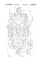
- FIG. 1is a block schematic diagram of an AC matrix addressed TFEL panel employing the scanning electrode network of the present invention.
- FIG. 2is a waveform diagram illustrating the method of operation of the scanning electrode network shown in FIG. 1.
- An AC matrix addressed TFEL display deviceincludes a panel 10.
- the panel 10includes a glass substrate (not shown separately) supporting a thin film electroluminescent layer sandwiched between insulator layers (not separately shown).
- This type of structureis well-known in the art as shown, for example, in Barrow et al., U.S. Pat. No. 4,719,385 "MULTI-COLORED THIN-FILM ELECTROLUMINESCENT DISPLAY," Jan. 12, 1988.
- top column electrodes 12which function as data electrodes are aligned across the panel from top to bottom and extend from the top towards the middle of the panel for a distance slightly less than halfway across.
- Bottom column electrodes 14extend from the bottom of the panel 10 towards the middle in lines which are colinear with respective ones of the top column electrodes 12. This construction is generally in accordance with the split-screen architecture of the Dolinar et al. '320 patent cited above.
- the column electrodes 12 and 14are driven, respectively, by top column drivers 16 and bottom column drivers 18.
- a set of left top row drivers 20drives the odd-numbered scanning electrodes 22 in the top half 10a of the panel 10.
- a left bottom row driver 24drives the odd-numbered scanning electrodes 26 in the bottom half 10b of the panel 10.
- Top even-numbered scanning electrodes 28are driven by a set of right top row drivers 30 and the bottom even-numbered scanning electrodes 32 are driven by a set of right bottom row drivers 34.
- a left row composite network 36provides a power signal on line 38 to both the left top row drivers 20 and the left bottom row drivers 24.
- the left row composite networkalso includes a logic section 36a which provides enable signals on lines 40a and 40b to the left top row drivers 20 and the left bottom row drivers 24, respectively.
- a right row composite network 42provides a power signal to the right top row drivers 30 and to the right bottom row drivers 34 on line 44.
- a logic section 42a of the right row composite 42includes enable lines 46a and 46b which control the gating of the power signal onto the electrodes 28 and 32 through the right top row drivers 30 and the right bottom row drivers 34.
- a column loading control 48receives inputs from a bottom column load line 50 and a top column load line 52. Depending upon the number of columns that are energized during the scanning of each row, the column loading control 48 provides a signal to both the right row composite 42 and the left row composite 36. Because energized column electrodes provide more capacitance and, hence, present a higher capacitive load to the left and right row composites 36 and 42, the signal from the column loading control 48 alters the pulse width of the power signal provided by the left and right row composites accordingly.
- FIG. 2illustrates the method of operation of the scanning sequence.
- the row electrodes in the top and bottom halves of the panel 10are energized in line-by-line sequence.
- the device of FIG. 1may contain 864 row electrodes.
- row 1, which lies in the top half of the screenis scanned with a positive voltage
- row 434 which lies in the bottom half of the screenis scanned with a negative voltage.
- row 2, which lies in the top half of the panelis scanned with a negative voltage.
- row 433 which lies in the bottom half of the panelis scanned with a positive voltage. This sequence continues until a frame has been completed.
- the polarityis reversed and the odd-numbered rows, which are driven from the left hand side of the screen, are scanned negatively while the even-numbered rows are scanned with a positive voltage.
- Two rowsare always scanned simultaneously, one being odd and the other being even, and situated in opposite halves of the panel, but are scanned with voltages of differing polarities to decrease the peak power requirements for the power supply driving the composite networks 36 and 42, respectively. This enables components of the power supplies to be made smaller relative to the size of the panel. The end result is that the panels may be made larger since the power supplies are capable of providing a higher current.
- the data logic for the column electrodesis different for the top column drivers 16 and the bottom column drivers 18, respectively.
- the top column driver outputwould be high.
- the bottom driver column outputwould be low, however, to illuminate a pixel in row 433 at the same time that a pixel in row 2 were being illuminated.
- the layout of the electrodeshas been described in terms of the conventional manner of assigning functions to the electrodes.
- the scanning electrodesare generally laid out as horizontal rows and the data electrodes are vertical columns.
- the inventionis not limited to any such layout and applies equally to scanning and data function electrodes which may be laid out vertically and horizontally, respectively, or even patterned in some unorthodox manner.
- the terms "row,” “column,” “top” and “bottom”are relative and the invention does not depend upon the particular orientation of the panel, but only upon the functions of the components therein.
- Appropriate voltage levels for generating the wave forms in FIG. 2are +210 volts for the positive row scanning voltages, -160 volts for the negative row scanning voltages, and +50 volts or zero for the column voltages,
- +210 voltsfor the positive row scanning voltages
- -160 voltsfor the negative row scanning voltages
- +50 volts or zerofor the column voltages
Landscapes
- Engineering & Computer Science (AREA)
- Physics & Mathematics (AREA)
- Computer Hardware Design (AREA)
- General Physics & Mathematics (AREA)
- Theoretical Computer Science (AREA)
- Control Of Indicators Other Than Cathode Ray Tubes (AREA)
Abstract
Description
This application is a continuation-in-part of application Ser. No. 166,417 entitled "Symmetric Drive Network For A TFEL Panel" filed Mar. 10, 1988, now abandoned, and is assigned to the same assignee.
The following invention relates to a method and apparatus for energizing the scanning electrodes of a matrix-addressed AC TFEL panel in a way that conserves energy and allows for the use of larger panels.
Conventional AC matrix-addressed TFEL panels include a set of scanning electrodes and a set of data electrodes sandwiching an electroluminesscent (EL) phosphor laminate. In general, selected data electrodes are energized as the scanning electrodes are energized a line at a time. Once all of the scanning electrodes have been energized in this fashion, a frame of data has been completed. Usually the scanning electrodes are arranged as row electrodes extending from right to left and all are connected to a power source which comprises a high current power IC to provide the scanning voltage. The scanning voltage is selectively gated onto each individual row electrode by individual row driver transistors which act as switches under the control of logic circuits. An example of the way in which the electrodes of this type are conventionally arranged is shown in the U.S. Patent to Kinoshita, et al., U.S. Pat. No. 4,485,379.
An improvement to such conventional TFEL panels is shown in Dolinar, et al., U.S. Pat. No. 4,739,320 which is assigned to the assignee of the present application. The Dolinar, et al. patent discloses a split screen architecture for matrix-addressed AC TFEL panels in which the column drivers are split into top and bottom segments which are separately driven. This enables the row drivers to drive top and bottom row electrodes simultaneously. This conserves energy in the panel and provides for a higher frame repetition rate because of the time savings realized by scanning the top and bottom portions of the screen simultaneously. A drawback to the design of Dolinar, et al. is that the row drivers are driven with the same polarity both in the top and bottom sectors of the screen simultaneously. This places demands on the power supply powering the row driver IC's, and the result is that the power supplies must be made physically large to accommodate the peak energy requirements. This in turn has negative consequences for the overall size of the panel because long electrodes are required for larger panel sizes resulting in a corresponding need for an increase in the size of the power supply. TFEL panels provide an advantage over conventional cathode ray tube displays because of their compact size. If a very large power supply is required, however, this advantage becomes diminished.
A variation of the Dolinar, et al. driving scheme is shown in Flegal, U.S. Pat. No. 4,733,228 assigned to the same assignee and which is incorporated herein by reference. The Flegal patent discloses a symmetric drive scheme where the scanning electrodes are alternately driven positive and negative on alternating frames. A still further variation of this concept is shown in U.S. patent application Ser. No. 166,417 also assigned to the same assignee and now abandoned. According to this application, the row or scanning electrodes alternate between driving voltages of positive and negative polarity as the rows are scanned from top to bottom and polarities are reversed every frame. The problem with this approach is that if the electrodes are arranged in the manner suggested by the Dolinar, et al. '320 patent, the positive and negative power supplies would still be called upon to deliver twice the power for every row electrode that is scanned because the electrodes are connected to the power supply in complementary top and bottom pairs.
A desirable object in the design of such panels would be to utilize split screen architecture along with line by line symmetric drive while at the same time decreasing the overall power requirements for the scanning electrodes, thus permitting a more compact electronics package. This would also enable larger panels to be fabricated without an attendant increase in the size of the power supplies.
The present invention provides a method and apparatus for energizing the scanning electrodes of an AC TFEL matrix-addressed panel in a way that conserves energy and permits conventionally sized electronics components to drive a larger TFEL display. The scanning electrodes are divided into two primary groups, those driven from the left side of the panel and those driven from the right side of the panel. The electrodes in these groups are interleaved in alternating fashion across the panel from top to bottom. In addition, the left and right side scanning electrodes, which may be viewed as odd and even row electrodes, respectively, are divided into two subsets, one of which is located in the top half of the panel and the other of which is located in the bottom half. The panel employs split screen architecture, and as such, the data or column electrodes are divided into colinearly aligned complimentary pairs extending towards each other from opposite sides of the panel for a distance slightly less than halfway across the screen.
The top and bottom halves of the screen are driven simultaneously, and in accordance with the invention, the rows are scanned in line-by-line fashion where a row in the top half of the panel is scanned with a first polarity voltage when, simultaneously, a row in the bottom half of the panel is scanned with an opposite polarity voltage. For example, all odd rows may be scanned with a negative voltage on a first frame, while all even rows are scanned with a positive voltage on the same frame. On the next frame the polarity may be reversed so that the odd rows are scanned with a positive voltage and the even rows are scanned with a negative voltage. Moreover, an odd row located in, for example, the top half of the panel may be scanned simultaneously with the scanning of an even numbered row located in the bottom half of the panel. This provides for the simultaneous scanning of bottom and top halves of the panel while using less energy than would be required for the same type of scanning using the drive scheme of U.S. Pat. No. 4,739,320 mentioned above. This is because a positive power supply drives one electrode while a negative power supply drives the other. This reduces the power required because the demand is divided between positive and negative supplies, while the top and bottom scanning electrodes are energized simultaneously. This provides the advantages of split screen architecture and alternate line symmetric drive scanning while reducing the peak energy requirements for the scanning electrode power supplies.
It is a principal object of this invention to provide a method and apparatus for scanning an AC matrix-addressed TFEL panel having split screen architecture and utilizing symmetric drive techniques to conserve energy, simplify the electronics layout for the panel, and provide higher current for the scanning electrodes thus enabling larger panels to be constructed.
The foregoing and other objectives, features and advantages of the present invention will be more readily understood upon consideration of the following detailed description of the invention taken in conjunction with the accompanying drawings.
FIG. 1 is a block schematic diagram of an AC matrix addressed TFEL panel employing the scanning electrode network of the present invention.
FIG. 2 is a waveform diagram illustrating the method of operation of the scanning electrode network shown in FIG. 1.
An AC matrix addressed TFEL display device includes apanel 10. Thepanel 10 includes a glass substrate (not shown separately) supporting a thin film electroluminescent layer sandwiched between insulator layers (not separately shown). This type of structure is well-known in the art as shown, for example, in Barrow et al., U.S. Pat. No. 4,719,385 "MULTI-COLORED THIN-FILM ELECTROLUMINESCENT DISPLAY," Jan. 12, 1988.
A set oftop column electrodes 12 which function as data electrodes are aligned across the panel from top to bottom and extend from the top towards the middle of the panel for a distance slightly less than halfway across.Bottom column electrodes 14 extend from the bottom of thepanel 10 towards the middle in lines which are colinear with respective ones of thetop column electrodes 12. This construction is generally in accordance with the split-screen architecture of the Dolinar et al. '320 patent cited above. Thecolumn electrodes top column drivers 16 andbottom column drivers 18.
A set of lefttop row drivers 20 drives the odd-numberedscanning electrodes 22 in thetop half 10a of thepanel 10. A leftbottom row driver 24 drives the odd-numberedscanning electrodes 26 in thebottom half 10b of thepanel 10. Top even-numberedscanning electrodes 28 are driven by a set of righttop row drivers 30 and the bottom even-numberedscanning electrodes 32 are driven by a set of rightbottom row drivers 34. A left row composite network 36 provides a power signal online 38 to both the lefttop row drivers 20 and the leftbottom row drivers 24. The left row composite network also includes alogic section 36a which provides enable signals onlines 40a and 40b to the lefttop row drivers 20 and the leftbottom row drivers 24, respectively. Similarly, on the right side of thepanel 10, a right rowcomposite network 42 provides a power signal to the righttop row drivers 30 and to the rightbottom row drivers 34 online 44. Alogic section 42a of theright row composite 42 includes enablelines electrodes top row drivers 30 and the rightbottom row drivers 34.
Acolumn loading control 48 receives inputs from a bottomcolumn load line 50 and a topcolumn load line 52. Depending upon the number of columns that are energized during the scanning of each row, thecolumn loading control 48 provides a signal to both theright row composite 42 and the left row composite 36. Because energized column electrodes provide more capacitance and, hence, present a higher capacitive load to the left andright row composites 36 and 42, the signal from thecolumn loading control 48 alters the pulse width of the power signal provided by the left and right row composites accordingly.
FIG. 2 illustrates the method of operation of the scanning sequence. The row electrodes in the top and bottom halves of thepanel 10 are energized in line-by-line sequence. For example, the device of FIG. 1 may contain 864 row electrodes. Thus, whenrow 1, which lies in the top half of the screen, is scanned with a positive voltage, an even-numbered row,row 434 which lies in the bottom half of the screen, is scanned with a negative voltage. On the next scan,row 2, which lies in the top half of the panel, is scanned with a negative voltage. Simultaneously,row 433 which lies in the bottom half of the panel, is scanned with a positive voltage. This sequence continues until a frame has been completed. At this point the polarity is reversed and the odd-numbered rows, which are driven from the left hand side of the screen, are scanned negatively while the even-numbered rows are scanned with a positive voltage. Two rows are always scanned simultaneously, one being odd and the other being even, and situated in opposite halves of the panel, but are scanned with voltages of differing polarities to decrease the peak power requirements for the power supply driving thecomposite networks 36 and 42, respectively. This enables components of the power supplies to be made smaller relative to the size of the panel. The end result is that the panels may be made larger since the power supplies are capable of providing a higher current.
Since the polarity of the rows being scanned in the top and bottom halves of the panel, reverses for each separate scan, the data logic for the column electrodes is different for thetop column drivers 16 and thebottom column drivers 18, respectively. For example, in a first frame, in order to illuminate a pixel inrow 2, the top column driver output would be high. The bottom driver column output would be low, however, to illuminate a pixel inrow 433 at the same time that a pixel inrow 2 were being illuminated.
Once theentire panel 10 has been scanned, that is, when all 864 rows have been "written" with a positive or negative power signal, the polarity reverses. This requires a corresponding reversal in the column driver logic. On the next frame, to illuminate pixels inRow 433, the bottom column drivers are high; to illuminate a pixel inrow 2, the top columns are low.
In general, the layout of the electrodes has been described in terms of the conventional manner of assigning functions to the electrodes. Thus, the scanning electrodes are generally laid out as horizontal rows and the data electrodes are vertical columns. However, the invention is not limited to any such layout and applies equally to scanning and data function electrodes which may be laid out vertically and horizontally, respectively, or even patterned in some unorthodox manner. Thus, the terms "row," "column," "top" and "bottom" are relative and the invention does not depend upon the particular orientation of the panel, but only upon the functions of the components therein.
Appropriate voltage levels for generating the wave forms in FIG. 2 are +210 volts for the positive row scanning voltages, -160 volts for the negative row scanning voltages, and +50 volts or zero for the column voltages, Thus, a combination of +210 on a row electrode and zero on certain columns will place a charge across those portions of the panel needed to illuminate selected pixels. However, at the same time a column charge of +50 volts will keep those particular pixels dark. This is due to the fact that for thepanel 10, 210 volts is just above the threshold of luminescence, but +160 (210v-50v) is not. Correspondingly when a negative (-160 volt) scan is used, those columns having a charge of +50 volts cause luminescence because the potential across the panel is -210 volts (-160v-50v), while those columns with zero voltage are below the threshold of luminescence at -160 volts.
The terms and expressions which have been employed in the foregoing specification are used therein as terms of description and not of limitation, and there is no intention, in the use of such terms and expressions, of excluding equivalents of the features shown and described or portions thereof, it being recognized that the scope of the invention is defined and limited only by the claims which follow.
Claims (5)
1. A scanning network for a matrix-addressed AC TFEL panel comprising first and second pluralities of scanning electrodes alternately interleaved with respect to each other across said panel, said first plurality connected to a first power source and said second plurality connected to a second power source, first and second pluralities of data electrodes, said first plurality of data electrodes occupying a first half portion of said panel and said second plurality of data electrodes occupying a second half portion of said panel, each plurality of said electrodes comprising an array of parallel electrode members disposed at right angles to said first and second pluralities of scanning electrodes and extending slightly less than halfway across said panel in the respective half portions thereof, and logic means for energizing a scanning electrode in said first plurality located in said first half portion of said panel with a positive power signal while simultaneously energizing a different scanning electrode in said second plurality located in said second half portion of said panel with a negative power signal.
2. The scanning network of claim 1 wherein said first and second pluralities of electrodes each comprise first and second electrode subsets wherein electrodes in each of said first and second subsets are scanned in line by line fashion simultaneously.
3. A method of energizing the scanning electrodes of a matrix-addressed AC TFEL panel wherein said panel comprises data electrodes having a first set of elongate parallel conductive strips extending slightly less than halfway across said panel from a first edge thereof to occupy a first half portion of said panel, and a second set of elongate parallel conductive strips extending slightly less than halfway across said panel from a second and opposite edge thereof to occupy a second half portion of said panel, and wherein said panel includes first and second sets of scanning electrodes disposed at right angles to said data electrodes and alternately interleaved across said panel, comprising the steps of:
(a) during a first frame of data: energizing said scanning electrodes in said first and second sets in line by line fashion wherein a first electrode in said first set and situated in said first half portion of said panel is energized with a signal of a first polarity simultaneously with energizing a second electrode in said second set situated in said second half portion of said panel with a signal of an opposite polarity; and
(b) during a next frame of data: Energizing the electrodes in said first and second sets of scanning electrodes in line by line fashion wherein said first electrode in said first set is energized with a signal of said opposite polarity simultaneously with energizing said second electrode in said second set with a signal of said first polarity.
4. The method of claim 3 wherein said signal of said first polarity is a positive voltage and said signal of said second polarity is a negative voltage.
5. The method of claim 4 wherein said first and second sets of electrodes each comprise top and bottom electrode subsets, wherein one electrode from a top subset is energized simultaneously with one electrode from a bottom subset.
Priority Applications (2)
| Application Number | Priority Date | Filing Date | Title |
|---|---|---|---|
| US07/221,747US4982183A (en) | 1988-03-10 | 1988-07-19 | Alternate polarity symmetric drive for scanning electrodes in a split-screen AC TFEL display device |
| JP18483489AJP2894729B2 (en) | 1988-07-19 | 1989-07-19 | Scanning network for thin film electroluminescent display and driving method thereof |
Applications Claiming Priority (2)
| Application Number | Priority Date | Filing Date | Title |
|---|---|---|---|
| US16641788A | 1988-03-10 | 1988-03-10 | |
| US07/221,747US4982183A (en) | 1988-03-10 | 1988-07-19 | Alternate polarity symmetric drive for scanning electrodes in a split-screen AC TFEL display device |
Related Parent Applications (1)
| Application Number | Title | Priority Date | Filing Date |
|---|---|---|---|
| US16641788AContinuation-In-Part | 1988-03-10 | 1988-03-10 |
Publications (1)
| Publication Number | Publication Date |
|---|---|
| US4982183Atrue US4982183A (en) | 1991-01-01 |
Family
ID=26862248
Family Applications (1)
| Application Number | Title | Priority Date | Filing Date |
|---|---|---|---|
| US07/221,747Expired - LifetimeUS4982183A (en) | 1988-03-10 | 1988-07-19 | Alternate polarity symmetric drive for scanning electrodes in a split-screen AC TFEL display device |
Country Status (1)
| Country | Link |
|---|---|
| US (1) | US4982183A (en) |
Cited By (22)
| Publication number | Priority date | Publication date | Assignee | Title |
|---|---|---|---|---|
| WO1993006585A1 (en)* | 1991-09-17 | 1993-04-01 | Copytele, Inc. | Method for writing data to an electrophoretic display panel |
| US5410219A (en)* | 1991-02-05 | 1995-04-25 | Matsushita Electronics Corporation | Plasma display panel and a method for driving the same |
| US5416494A (en)* | 1991-12-24 | 1995-05-16 | Nippondenso Co., Ltd. | Electroluminescent display |
| US5646641A (en)* | 1993-07-06 | 1997-07-08 | Olympus Optical Co., Ltd. | Image display apparatus |
| US5812104A (en)* | 1992-06-30 | 1998-09-22 | Northrop Grumman Corporation | Gray-scale stepped ramp generator with individual step correction |
| JP3002537B2 (en) | 1991-09-17 | 2000-01-24 | コピイテル,インコーポレイテッド | Method for writing data to electrophoretic display panel |
| US6124853A (en)* | 1996-09-03 | 2000-09-26 | Lear Automotive Dearborn, Inc. | Power dissipation control for a visual display screen |
| USRE37069E1 (en) | 1991-10-17 | 2001-02-27 | Chips & Technologies, Llc | Data stream converter with increased grey levels |
| US6246385B1 (en)* | 1997-04-28 | 2001-06-12 | Matsushita Electric Industrial Co., Ltd. | Liquid crystal display device and its driving method |
| EP1148467A2 (en) | 2000-04-18 | 2001-10-24 | Semiconductor Energy Laboratory Co., Ltd. | Light emitting device |
| US20020003517A1 (en)* | 2000-04-28 | 2002-01-10 | Shouzou Ashizawa | Device and method for driving EL device |
| WO2002043032A3 (en)* | 2000-11-21 | 2003-05-30 | Avery Dennison Corp | Display device and methods of manufacture and control |
| US6573880B1 (en)* | 1999-11-16 | 2003-06-03 | Xerox Corporation | Applications for electronic reusable paper |
| US20030214229A1 (en)* | 2000-11-21 | 2003-11-20 | Holman Andrew W. | Display device and methods of manufacture and control |
| US20040239586A1 (en)* | 2003-05-30 | 2004-12-02 | Eastman Kodak Company | Flexible display |
| US20050057462A1 (en)* | 2000-10-13 | 2005-03-17 | Atsushi Kota | Image display apparatus with driving modes and method of driving the same |
| US20050284984A1 (en)* | 2002-08-13 | 2005-12-29 | De Lauzun Frederic | Visual display provided with secured electronic architecture |
| EP1724747A1 (en)* | 2005-05-17 | 2006-11-22 | LG Electronics Inc. | Light emitting device and method of driving the same |
| US20070109290A1 (en)* | 2005-11-15 | 2007-05-17 | Lg Electronics Inc. | Display device having plurality of power supplies and method for controlling the same |
| US20090040202A1 (en)* | 2007-08-10 | 2009-02-12 | Samsung Electronics Co., Ltd. | Drive circuit and liquid crystal display apparatus including the same |
| US20150170561A1 (en)* | 2013-12-17 | 2015-06-18 | Samsung Display Co., Ltd. | Display device and method of driving the same |
| US20170115802A1 (en)* | 2015-10-22 | 2017-04-27 | Xiamen Tianma Micro-Electronics Co., Ltd. | Array substrate, touch display device and method for driving the same |
Citations (12)
| Publication number | Priority date | Publication date | Assignee | Title |
|---|---|---|---|---|
| US4338598A (en)* | 1980-01-07 | 1982-07-06 | Sharp Kabushiki Kaisha | Thin-film EL image display panel with power saving features |
| US4468659A (en)* | 1980-08-25 | 1984-08-28 | Sharp Kabushiki Kaisha | Electroluminescent display panel assembly |
| US4485379A (en)* | 1981-02-17 | 1984-11-27 | Sharp Kabushiki Kaisha | Circuit and method for driving a thin-film EL panel |
| GB2161011A (en)* | 1984-05-23 | 1986-01-02 | Sharp Kk | EL display arrangements |
| GB2165078A (en)* | 1984-09-28 | 1986-04-03 | Sharp Kk | Thin-film el display panel drive circuit |
| US4586039A (en)* | 1982-04-26 | 1986-04-29 | Sharp Kabushiki Kaisha | Liquid crystal display device and method for driving thereof |
| US4716341A (en)* | 1985-01-07 | 1987-12-29 | Nec Corporation | Display device |
| US4733228A (en)* | 1985-07-31 | 1988-03-22 | Planar Systems, Inc. | Transformer-coupled drive network for a TFEL panel |
| US4739320A (en)* | 1985-04-30 | 1988-04-19 | Planar Systems, Inc. | Energy-efficient split-electrode TFEL panel |
| US4816816A (en)* | 1985-06-17 | 1989-03-28 | Casio Computer Co., Ltd. | Liquid-crystal display apparatus |
| US4823121A (en)* | 1985-10-15 | 1989-04-18 | Sharp Kabushiki Kaisha | Electroluminescent panel driving system for driving the panel's electrodes only when non-blank data is present to conserve power |
| US4830466A (en)* | 1985-03-15 | 1989-05-16 | Sharp Kabushiki Kaisha | Drive system for an active matrix liquid crystal display panel having divided row electrodes |
- 1988
- 1988-07-19USUS07/221,747patent/US4982183A/ennot_activeExpired - Lifetime
Patent Citations (13)
| Publication number | Priority date | Publication date | Assignee | Title |
|---|---|---|---|---|
| US4338598A (en)* | 1980-01-07 | 1982-07-06 | Sharp Kabushiki Kaisha | Thin-film EL image display panel with power saving features |
| US4468659A (en)* | 1980-08-25 | 1984-08-28 | Sharp Kabushiki Kaisha | Electroluminescent display panel assembly |
| US4485379A (en)* | 1981-02-17 | 1984-11-27 | Sharp Kabushiki Kaisha | Circuit and method for driving a thin-film EL panel |
| US4586039A (en)* | 1982-04-26 | 1986-04-29 | Sharp Kabushiki Kaisha | Liquid crystal display device and method for driving thereof |
| GB2161011A (en)* | 1984-05-23 | 1986-01-02 | Sharp Kk | EL display arrangements |
| US4686426A (en)* | 1984-09-28 | 1987-08-11 | Sharp Kabushiki Kaisha | Thin-film EL display panel drive circuit with voltage compensation |
| GB2165078A (en)* | 1984-09-28 | 1986-04-03 | Sharp Kk | Thin-film el display panel drive circuit |
| US4716341A (en)* | 1985-01-07 | 1987-12-29 | Nec Corporation | Display device |
| US4830466A (en)* | 1985-03-15 | 1989-05-16 | Sharp Kabushiki Kaisha | Drive system for an active matrix liquid crystal display panel having divided row electrodes |
| US4739320A (en)* | 1985-04-30 | 1988-04-19 | Planar Systems, Inc. | Energy-efficient split-electrode TFEL panel |
| US4816816A (en)* | 1985-06-17 | 1989-03-28 | Casio Computer Co., Ltd. | Liquid-crystal display apparatus |
| US4733228A (en)* | 1985-07-31 | 1988-03-22 | Planar Systems, Inc. | Transformer-coupled drive network for a TFEL panel |
| US4823121A (en)* | 1985-10-15 | 1989-04-18 | Sharp Kabushiki Kaisha | Electroluminescent panel driving system for driving the panel's electrodes only when non-blank data is present to conserve power |
Cited By (34)
| Publication number | Priority date | Publication date | Assignee | Title |
|---|---|---|---|---|
| US5410219A (en)* | 1991-02-05 | 1995-04-25 | Matsushita Electronics Corporation | Plasma display panel and a method for driving the same |
| JP3002537B2 (en) | 1991-09-17 | 2000-01-24 | コピイテル,インコーポレイテッド | Method for writing data to electrophoretic display panel |
| WO1993006585A1 (en)* | 1991-09-17 | 1993-04-01 | Copytele, Inc. | Method for writing data to an electrophoretic display panel |
| USRE37069E1 (en) | 1991-10-17 | 2001-02-27 | Chips & Technologies, Llc | Data stream converter with increased grey levels |
| US5416494A (en)* | 1991-12-24 | 1995-05-16 | Nippondenso Co., Ltd. | Electroluminescent display |
| US5812104A (en)* | 1992-06-30 | 1998-09-22 | Northrop Grumman Corporation | Gray-scale stepped ramp generator with individual step correction |
| US5646641A (en)* | 1993-07-06 | 1997-07-08 | Olympus Optical Co., Ltd. | Image display apparatus |
| US6124853A (en)* | 1996-09-03 | 2000-09-26 | Lear Automotive Dearborn, Inc. | Power dissipation control for a visual display screen |
| US6246385B1 (en)* | 1997-04-28 | 2001-06-12 | Matsushita Electric Industrial Co., Ltd. | Liquid crystal display device and its driving method |
| US6573880B1 (en)* | 1999-11-16 | 2003-06-03 | Xerox Corporation | Applications for electronic reusable paper |
| EP1148467A2 (en) | 2000-04-18 | 2001-10-24 | Semiconductor Energy Laboratory Co., Ltd. | Light emitting device |
| EP1148467A3 (en)* | 2000-04-18 | 2009-06-10 | Semiconductor Energy Laboratory Co., Ltd. | Light emitting device |
| US6867755B2 (en)* | 2000-04-28 | 2005-03-15 | Yazaki Corporation | Device and method for driving EL device |
| US20020003517A1 (en)* | 2000-04-28 | 2002-01-10 | Shouzou Ashizawa | Device and method for driving EL device |
| US20050057462A1 (en)* | 2000-10-13 | 2005-03-17 | Atsushi Kota | Image display apparatus with driving modes and method of driving the same |
| US7420551B2 (en)* | 2000-10-13 | 2008-09-02 | Samsung Sdi Co., Ltd. | Image display apparatus with driving modes and method of driving the same |
| US7199527B2 (en) | 2000-11-21 | 2007-04-03 | Alien Technology Corporation | Display device and methods of manufacturing and control |
| US20040004609A1 (en)* | 2000-11-21 | 2004-01-08 | Holman Andrew W. | Display device and methods of manufacture and control |
| WO2002043032A3 (en)* | 2000-11-21 | 2003-05-30 | Avery Dennison Corp | Display device and methods of manufacture and control |
| US20030214229A1 (en)* | 2000-11-21 | 2003-11-20 | Holman Andrew W. | Display device and methods of manufacture and control |
| US20050284984A1 (en)* | 2002-08-13 | 2005-12-29 | De Lauzun Frederic | Visual display provided with secured electronic architecture |
| US20040239586A1 (en)* | 2003-05-30 | 2004-12-02 | Eastman Kodak Company | Flexible display |
| US8665247B2 (en)* | 2003-05-30 | 2014-03-04 | Global Oled Technology Llc | Flexible display |
| US7598935B2 (en) | 2005-05-17 | 2009-10-06 | Lg Electronics Inc. | Light emitting device with cross-talk preventing circuit and method of driving the same |
| EP1724747A1 (en)* | 2005-05-17 | 2006-11-22 | LG Electronics Inc. | Light emitting device and method of driving the same |
| US20060262049A1 (en)* | 2005-05-17 | 2006-11-23 | Lg Electronics Inc. | Light emitting device and method of driving the same |
| EP1786201A3 (en)* | 2005-11-15 | 2009-01-21 | LG Electronics Inc. | Display device having plurality of power supplies and method for controlling the same |
| US7817147B2 (en) | 2005-11-15 | 2010-10-19 | Lg Electronics Inc. | Display device having plurality of power supplies and method for controlling the same |
| US20070109290A1 (en)* | 2005-11-15 | 2007-05-17 | Lg Electronics Inc. | Display device having plurality of power supplies and method for controlling the same |
| US20090040202A1 (en)* | 2007-08-10 | 2009-02-12 | Samsung Electronics Co., Ltd. | Drive circuit and liquid crystal display apparatus including the same |
| US8300034B2 (en)* | 2007-08-10 | 2012-10-30 | Samsung Electronics Co., Ltd. | Drive circuit and liquid crystal display apparatus including the same |
| US20150170561A1 (en)* | 2013-12-17 | 2015-06-18 | Samsung Display Co., Ltd. | Display device and method of driving the same |
| US20170115802A1 (en)* | 2015-10-22 | 2017-04-27 | Xiamen Tianma Micro-Electronics Co., Ltd. | Array substrate, touch display device and method for driving the same |
| US10133398B2 (en)* | 2015-10-22 | 2018-11-20 | Xiamen Tianma Micro-Electronics Co., Ltd. | Array substrate, touch display device and method for driving the same |
Similar Documents
| Publication | Publication Date | Title |
|---|---|---|
| US4982183A (en) | Alternate polarity symmetric drive for scanning electrodes in a split-screen AC TFEL display device | |
| US4888523A (en) | Driving circuit of thin membrane EL display apparatus | |
| CN106710562B (en) | A kind of display panel and display device | |
| EP0466378B1 (en) | Liquid crystal display panel for reduced flicker | |
| US5093655A (en) | Liquid-crystal display apparatus | |
| US6727875B1 (en) | High-definition liquid crystal display including sub scan circuit which separately controls plural pixels connected to the same main scan wiring line and the same sub scan wiring line | |
| US4114070A (en) | Display panel with simplified thin film interconnect system | |
| US8619007B2 (en) | Electro-luminescence display device for implementing compact panel and driving method thereof | |
| KR100561946B1 (en) | LCD and its driving method | |
| US4797667A (en) | Split screen electrode structure for TFEL panel | |
| JPH01202793A (en) | Matrix display device | |
| US8456398B2 (en) | Liquid crystal display module | |
| WO1989002144A1 (en) | Active matrix cell for ac operation | |
| US4739320A (en) | Energy-efficient split-electrode TFEL panel | |
| US4816819A (en) | Display panel | |
| US6646624B1 (en) | AC plasma display device | |
| KR20200030227A (en) | Display Device | |
| US7746306B2 (en) | Display device having an improved video signal drive circuit | |
| US20030107544A1 (en) | Display devices and driving method therefor | |
| US5029257A (en) | Method for separating scan line drive in plasma display panel and circuit arrangement thereof | |
| CN1823367A (en) | Active matrix array device | |
| WO2006027754A1 (en) | Apparatus for driving matrix-type lcd panels and a liquid crystal display based thereon | |
| EP0308214B1 (en) | Thin film electroluminescent display device | |
| WO2003083815A2 (en) | Liquid crystal display driving with dot-inversion | |
| JP3953544B2 (en) | EL display device |
Legal Events
| Date | Code | Title | Description |
|---|---|---|---|
| AS | Assignment | Owner name:PLANAR SYSTEMS, INC., 1400 N.W. COMPTON DR., BEAVE Free format text:ASSIGNMENT OF ASSIGNORS INTEREST.;ASSIGNORS:FLEGAL, ROBERT T.;ZIUCHKOVSKI, MICHAEL J.;REEL/FRAME:004933/0694 Effective date:19880627 Owner name:PLANAR SYSTEMS, INC.,OREGON Free format text:ASSIGNMENT OF ASSIGNORS INTEREST;ASSIGNORS:FLEGAL, ROBERT T.;ZIUCHKOVSKI, MICHAEL J.;REEL/FRAME:004933/0694 Effective date:19880627 | |
| STCF | Information on status: patent grant | Free format text:PATENTED CASE | |
| AS | Assignment | Owner name:PLANAR SYSTEMS, INC., 1400 N.W. COMPTON DRIVE, BEA Free format text:ASSIGNMENT OF ASSIGNORS INTEREST.;ASSIGNOR:PLANAR SYSTEMS, INC., A CORP OF DE;REEL/FRAME:005500/0972 Effective date:19881205 | |
| FPAY | Fee payment | Year of fee payment:4 | |
| FPAY | Fee payment | Year of fee payment:8 | |
| FPAY | Fee payment | Year of fee payment:12 |