US4978423A - Selective solder formation on printed circuit boards - Google Patents
Selective solder formation on printed circuit boardsDownload PDFInfo
- Publication number
- US4978423A US4978423AUS07/249,133US24913388AUS4978423AUS 4978423 AUS4978423 AUS 4978423AUS 24913388 AUS24913388 AUS 24913388AUS 4978423 AUS4978423 AUS 4978423A
- Authority
- US
- United States
- Prior art keywords
- solder
- layer
- photoresist
- conductive material
- copper
- Prior art date
- Legal status (The legal status is an assumption and is not a legal conclusion. Google has not performed a legal analysis and makes no representation as to the accuracy of the status listed.)
- Expired - Fee Related
Links
Images


Classifications
- H—ELECTRICITY
- H05—ELECTRIC TECHNIQUES NOT OTHERWISE PROVIDED FOR
- H05K—PRINTED CIRCUITS; CASINGS OR CONSTRUCTIONAL DETAILS OF ELECTRIC APPARATUS; MANUFACTURE OF ASSEMBLAGES OF ELECTRICAL COMPONENTS
- H05K3/00—Apparatus or processes for manufacturing printed circuits
- H05K3/30—Assembling printed circuits with electric components, e.g. with resistor
- H05K3/32—Assembling printed circuits with electric components, e.g. with resistor electrically connecting electric components or wires to printed circuits
- H05K3/34—Assembling printed circuits with electric components, e.g. with resistor electrically connecting electric components or wires to printed circuits by soldering
- H05K3/3457—Solder materials or compositions; Methods of application thereof
- H05K3/3473—Plating of solder
- H—ELECTRICITY
- H05—ELECTRIC TECHNIQUES NOT OTHERWISE PROVIDED FOR
- H05K—PRINTED CIRCUITS; CASINGS OR CONSTRUCTIONAL DETAILS OF ELECTRIC APPARATUS; MANUFACTURE OF ASSEMBLAGES OF ELECTRICAL COMPONENTS
- H05K3/00—Apparatus or processes for manufacturing printed circuits
- H05K3/02—Apparatus or processes for manufacturing printed circuits in which the conductive material is applied to the surface of the insulating support and is thereafter removed from such areas of the surface which are not intended for current conducting or shielding
- H05K3/06—Apparatus or processes for manufacturing printed circuits in which the conductive material is applied to the surface of the insulating support and is thereafter removed from such areas of the surface which are not intended for current conducting or shielding the conductive material being removed chemically or electrolytically, e.g. by photo-etch process
- H05K3/061—Etching masks
- H05K3/062—Etching masks consisting of metals or alloys or metallic inorganic compounds
- H—ELECTRICITY
- H05—ELECTRIC TECHNIQUES NOT OTHERWISE PROVIDED FOR
- H05K—PRINTED CIRCUITS; CASINGS OR CONSTRUCTIONAL DETAILS OF ELECTRIC APPARATUS; MANUFACTURE OF ASSEMBLAGES OF ELECTRICAL COMPONENTS
- H05K3/00—Apparatus or processes for manufacturing printed circuits
- H05K3/30—Assembling printed circuits with electric components, e.g. with resistor
- H05K3/32—Assembling printed circuits with electric components, e.g. with resistor electrically connecting electric components or wires to printed circuits
- H05K3/34—Assembling printed circuits with electric components, e.g. with resistor electrically connecting electric components or wires to printed circuits by soldering
- H05K3/3452—Solder masks
- H—ELECTRICITY
- H05—ELECTRIC TECHNIQUES NOT OTHERWISE PROVIDED FOR
- H05K—PRINTED CIRCUITS; CASINGS OR CONSTRUCTIONAL DETAILS OF ELECTRIC APPARATUS; MANUFACTURE OF ASSEMBLAGES OF ELECTRICAL COMPONENTS
- H05K2201/00—Indexing scheme relating to printed circuits covered by H05K1/00
- H05K2201/09—Shape and layout
- H05K2201/09818—Shape or layout details not covered by a single group of H05K2201/09009 - H05K2201/09809
- H05K2201/099—Coating over pads, e.g. solder resist partly over pads
- H—ELECTRICITY
- H05—ELECTRIC TECHNIQUES NOT OTHERWISE PROVIDED FOR
- H05K—PRINTED CIRCUITS; CASINGS OR CONSTRUCTIONAL DETAILS OF ELECTRIC APPARATUS; MANUFACTURE OF ASSEMBLAGES OF ELECTRICAL COMPONENTS
- H05K2203/00—Indexing scheme relating to apparatus or processes for manufacturing printed circuits covered by H05K3/00
- H05K2203/03—Metal processing
- H05K2203/0361—Stripping a part of an upper metal layer to expose a lower metal layer, e.g. by etching or using a laser
- H—ELECTRICITY
- H05—ELECTRIC TECHNIQUES NOT OTHERWISE PROVIDED FOR
- H05K—PRINTED CIRCUITS; CASINGS OR CONSTRUCTIONAL DETAILS OF ELECTRIC APPARATUS; MANUFACTURE OF ASSEMBLAGES OF ELECTRICAL COMPONENTS
- H05K2203/00—Indexing scheme relating to apparatus or processes for manufacturing printed circuits covered by H05K3/00
- H05K2203/04—Soldering or other types of metallurgic bonding
- H05K2203/043—Reflowing of solder coated conductors, not during connection of components, e.g. reflowing solder paste
- H—ELECTRICITY
- H05—ELECTRIC TECHNIQUES NOT OTHERWISE PROVIDED FOR
- H05K—PRINTED CIRCUITS; CASINGS OR CONSTRUCTIONAL DETAILS OF ELECTRIC APPARATUS; MANUFACTURE OF ASSEMBLAGES OF ELECTRICAL COMPONENTS
- H05K3/00—Apparatus or processes for manufacturing printed circuits
- H05K3/10—Apparatus or processes for manufacturing printed circuits in which conductive material is applied to the insulating support in such a manner as to form the desired conductive pattern
- H05K3/108—Apparatus or processes for manufacturing printed circuits in which conductive material is applied to the insulating support in such a manner as to form the desired conductive pattern by semi-additive methods; masks therefor
Definitions
- This inventionrelates to the fabrication of printed circuit boards.
- copper conductorsare formed over the board by electroless deposition of a thin copper layer followed by selective electroplanting of a thick copper layer in the desired conductive pattern utilizing a photoresist.
- a solder layeris usually applied uniformly over the electroplated copper to act as an etch resist.
- a dry film solder maskis applied over the structure and the board is ready for mounting of semiconductor components. If it is desired to have solder in selected areas, the solder is deposited by screen printing.
- solderis desired on selected portions of the copper conductor
- present screen printing techniquesare usually adequate.
- certain applicationsrequire very dense conductor arrays (i.e., typically less than 625 ⁇ m pitch). For such spacing, a more accurate method of providing solder selectively on the conductors is desired.
- the inventionis a method for fabricating printed circuit boards.
- a pattern of conductive materialis formed over an insulating substrate, and a layer of solder is deposited over the conductive pattern.
- a photoresist maskis formed over the resulting structure so as to expose areas of solder to be removed, and these exposed areas are then selectively removed. If desired, the conductive material exposed by the solder removal can be scrubbed while the photoresist acts to protect the remaining portions of the solder.
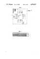
- FIG. 1is a plan view of a portion of a printed circuit board fabricated in accordance with an embodiment of the invention.
- FIGS. 2-10are cross-sectional views of a portion of the printed circuit board during various stages of fabrication in accordance with the same embodiment.
- FIG. 1illustrates a portion of a printed circuit board suitable for bonding a semiconductor component (not shown). It will be appreciated that this portion is shown for illustrative purposes only, and the board would include many more conductor paths and components.
- the board, 10,includes a set of conductors, e.g., 21, which are formed in close proximity to each other.
- the center-to-center spacing (pitch)is 400 ⁇ m and the invention is most useful when the pitch is less than 625 ⁇ m.
- the conductorswill be electrically connected to the semiconductor component mounted to the board by means of stantard procedures such as tape automated bonding (TAB).
- TABtape automated bonding
- bonding areas, 22,are formed near the edge of the conductors in order to bond the tape members from the semiconductor component to the conductors.
- the bonding areas, 22,include a layer of solder formed on the conductors as described in more detail below.
- FIGS. 2-10are cross-sectional views along line 2--2' of FIG. 1 showing a conductor during various stages of fabrication.
- the board, 10,is first entirely covered by a thin layer, 16, of copper formed by electroplating and a thin layer of copper, 11, formed by a standard electroless deposition.
- the copper layer, 16,is approximately 18 ⁇ m thick and the upper layer, 11, is approximately 2.5 ⁇ m thick.
- a first photoresist layer, 12,was formed over essentially the entire surface of the copper layers and then developed by standard photolithographic techniques to expose an appropriate pattern.
- the photoresistis typically an aqueous resist such as Dynachem HG which is laminated onto the layer, 11, to a thickness of approximately 50 ⁇ m.
- the structurewas then subjected to a copper electroplating so that copper layers, such as 13, were formed on the exposed areas of the electroless copper layer 11.
- This copper layer, which defines the conductor pattern in the final circuit board,was approximately 25-35 ⁇ m thick and could, generally, be in the range 25-50 ⁇ m. Standard electroplating techniques were utilized.
- a layer 14, of solderwas electroplated onto the copper layer 13.
- the thickness and composition of this solder layerwill depend on the particular type of bonding employed for the semiconductor component. For the case of TAB bonding, it has been found that a thickness of at least approximately 7.5 ⁇ m is desirable to achieve an appropriate final, reflowed thickness of the solder layers.
- the particular solder employedwas tin-lead solder, with the tin component between 55 and 80% by weight, the remainder lead.
- the photoresist layer, 12,was then stripped off using a solution which does not attack solder, such as an ethanol amine solution, in particular that sold by Inland Chemical Corporation under the designation 6055.
- a typical etchantis a near neutral PH alkaline etchant such as ultra Etch-Fine line from MacDermid Corporation.
- a second photoresist layer, 15,was then formed over the board and conductor pattern including the plated solder layer 14.
- the boardPrior to deposition the board was UV heated to a temperature so that the surface of the board was in the range 38°-48° C. Conformance the photoresist to the features on the board and good adhesion to the solder layer as well as to the board surface are extremely important for ensuring a well-defined solder stripping in the following steps.
- the photoresist layeris deposited by vacuum lamination to a thickness in the range 75-100 ⁇ m to satisfy these requirements.
- the resistwas Dynachem TA. The temperature during the lamination was in the range 90°-100° C. and the pressure was 0.5-0.8 millibars for a time of 60-70 sec.
- solder layer, 14After photoresist layer, 15, was fully developed, as shown in FIG. 8, the exposed portions of solder layer, 14, were selectively removed leaving the solder portions, 22, protected by the photoresist on the copper layer 13.
- the solderwas selectively etched utilizing an etchant comprising hydrogen peroxide such as Enthone TL-143 which was applied by spray for a period of approximately 10 sec.
- the exposed portions of the copper layer, 13,were subject to a pumice scrubbing in order to micro-roughen the copper surface in preparation for solder mask adhesion.
- Thisbasically involves applying a silica mixture with nylon brushes to the entire structure in order to clean the copper surfaces.
- the specific gravity of the pumice mixturewas 1.075-1.125, gms/cm 3 . Cleaning usually is done for a period of approximately 5 sec.
- the photoresist layer, 15,protects the remaining solder portions, 22, from the abrasive action of the silica and brushes. Thus, it is important that the photoresist layer can withstand the scrubbing and maintain adherence to the solder layer during this cleaning operation.
- the photoresistwas stripped off to leave the structure shown in FIG. 9.
- the resistmust be stripped without significantly reducing the remaining solder portions 22.
- the particular stripping solution employedwas an ethanol-amine solution including an inhibitor, anti-oxidant and chelator such as that sold by Inland Chemical under the designation 6055. It will be appreciated that other photoresists and stripping solutions may be employed in the inventive process.
- a standard commercially available dry film solder mask 17is usually vacuum laminated over the structure to a thickness of approximately 75 ⁇ m as shown in FIG. 10.
- the portions of the mask over the solder portionswere then removed by a standard aqueous developer such as sodium carbonate.
- the solder portions 22were reflowed by exposing the structure to an infrared source which sufficiently heats the solder to cause it to melt and cover the side walls of the copper layers 13, 11 and 16.
- the purpose of the solder maskis to keep the solder off the protected areas of the copper during subsequent assembly of the circuit.
- the boardis then ready for mounting of semiconductor components thereon.
- the inventioncan be used to selectively form solder on any type of conductor.
Landscapes
- Engineering & Computer Science (AREA)
- Manufacturing & Machinery (AREA)
- Microelectronics & Electronic Packaging (AREA)
- Metallurgy (AREA)
- Manufacturing Of Printed Wiring (AREA)
- Electric Connection Of Electric Components To Printed Circuits (AREA)
Abstract
Description
Claims (8)
Priority Applications (5)
| Application Number | Priority Date | Filing Date | Title |
|---|---|---|---|
| US07/249,133US4978423A (en) | 1988-09-26 | 1988-09-26 | Selective solder formation on printed circuit boards |
| CA000611477ACA1301952C (en) | 1988-09-26 | 1989-09-14 | Selective solder formation on printed circuit boards |
| DE68918210TDE68918210T2 (en) | 1988-09-26 | 1989-09-19 | Selective formation of solder on printed circuit boards. |
| EP89309479AEP0361752B1 (en) | 1988-09-26 | 1989-09-19 | Selective solder formation on printed circuit boards |
| JP1246630AJPH069299B2 (en) | 1988-09-26 | 1989-09-25 | Processing method of printed wiring board |
Applications Claiming Priority (1)
| Application Number | Priority Date | Filing Date | Title |
|---|---|---|---|
| US07/249,133US4978423A (en) | 1988-09-26 | 1988-09-26 | Selective solder formation on printed circuit boards |
Publications (1)
| Publication Number | Publication Date |
|---|---|
| US4978423Atrue US4978423A (en) | 1990-12-18 |
Family
ID=22942182
Family Applications (1)
| Application Number | Title | Priority Date | Filing Date |
|---|---|---|---|
| US07/249,133Expired - Fee RelatedUS4978423A (en) | 1988-09-26 | 1988-09-26 | Selective solder formation on printed circuit boards |
Country Status (5)
| Country | Link |
|---|---|
| US (1) | US4978423A (en) |
| EP (1) | EP0361752B1 (en) |
| JP (1) | JPH069299B2 (en) |
| CA (1) | CA1301952C (en) |
| DE (1) | DE68918210T2 (en) |
Cited By (19)
| Publication number | Priority date | Publication date | Assignee | Title |
|---|---|---|---|---|
| US5160579A (en)* | 1991-06-05 | 1992-11-03 | Macdermid, Incorporated | Process for manufacturing printed circuit employing selective provision of solderable coating |
| WO1993002831A1 (en)* | 1991-08-05 | 1993-02-18 | Motorola, Inc. | Solder plate reflow method for forming a solder bump on a circuit trace |
| US5733599A (en)* | 1996-03-22 | 1998-03-31 | Macdermid, Incorporated | Method for enhancing the solderability of a surface |
| US6200451B1 (en) | 1996-03-22 | 2001-03-13 | Macdermid, Incorporated | Method for enhancing the solderability of a surface |
| WO2002029135A1 (en)* | 2000-10-03 | 2002-04-11 | Macdermid, Incorporated | Method for enhancing the solderability of a surface |
| US6544397B2 (en) | 1996-03-22 | 2003-04-08 | Ronald Redline | Method for enhancing the solderability of a surface |
| US20030118742A1 (en)* | 1996-03-22 | 2003-06-26 | Macdermid, Incorporated | Method for enhancing the solderability of a surface |
| US20030209446A1 (en)* | 1999-02-17 | 2003-11-13 | Macdermid Incorporated | Method for enhancing the solderability of a surface |
| US6773757B1 (en) | 2003-04-14 | 2004-08-10 | Ronald Redline | Coating for silver plated circuits |
| US20040198044A1 (en)* | 2003-04-04 | 2004-10-07 | Sheng-Chuan Huang | Stacking photoresist image transferring method for fabricating a packaging substrate |
| US20060024430A1 (en)* | 2004-07-29 | 2006-02-02 | Enthone Inc. | Silver plating in electronics manufacture |
| US20060032668A1 (en)* | 1996-12-19 | 2006-02-16 | Ibiden Co., Ltd. | Printed circuit boards and method of producing the same |
| US20060099727A1 (en)* | 2004-10-21 | 2006-05-11 | Endicott Interconnect Technologies, Inc. | Method of making a circuitized substrate having a plurality of solder connection sites thereon |
| US20070090170A1 (en)* | 2005-10-20 | 2007-04-26 | Endicott Interconnect Technologies, Inc. | Method of making a circuitized substrate having a plurality of solder connection sites thereon |
| US7631798B1 (en) | 2008-10-02 | 2009-12-15 | Ernest Long | Method for enhancing the solderability of a surface |
| WO2012033568A1 (en) | 2010-09-10 | 2012-03-15 | Macdermid Acumen, Inc. | Method for treating metal surfaces |
| WO2013078077A2 (en) | 2011-11-22 | 2013-05-30 | Macdermid Acumen, Inc. | Method for treating metal surfaces |
| USRE45842E1 (en) | 1999-02-17 | 2016-01-12 | Ronald Redline | Method for enhancing the solderability of a surface |
| CN114143978A (en)* | 2021-12-27 | 2022-03-04 | 百强电子(深圳)有限公司 | Solder mask preparation process for selective surface fine treatment of thick copper plate |
Families Citing this family (3)
| Publication number | Priority date | Publication date | Assignee | Title |
|---|---|---|---|---|
| JPH04137083U (en)* | 1991-04-05 | 1992-12-21 | 村男 駒井 | printed wiring board |
| WO1994026081A1 (en)* | 1993-04-26 | 1994-11-10 | P.A.C. Di Bezzetto Sandro & C.S.N.C. | Process for producing printed circuit boards |
| FR2972597B1 (en)* | 2011-03-10 | 2014-08-01 | Thales Sa | METHOD FOR MANUFACTURING THE WIRING AREAS OF A PRINTED BOARD |
Citations (8)
| Publication number | Priority date | Publication date | Assignee | Title |
|---|---|---|---|---|
| US3240684A (en)* | 1962-02-21 | 1966-03-15 | Burroughs Corp | Method of etching rhodium plated metal layers and of making rhodium plated printed circuit boards |
| US3576630A (en)* | 1966-10-29 | 1971-04-27 | Nippon Electric Co | Photo-etching process |
| US4004956A (en)* | 1974-08-14 | 1977-01-25 | Enthone, Incorporated | Selectively stripping tin or tin-lead alloys from copper substrates |
| US4216246A (en)* | 1977-05-14 | 1980-08-05 | Hitachi Chemical Company, Ltd. | Method of improving adhesion between insulating substrates and metal deposits electrolessly plated thereon, and method of making additive printed circuit boards |
| US4306933A (en)* | 1980-02-11 | 1981-12-22 | Chemline Industries | Tin/tin-lead stripping solutions |
| US4319955A (en)* | 1980-11-05 | 1982-03-16 | Philip A. Hunt Chemical Corp. | Ammoniacal alkaline cupric etchant solution for and method of reducing etchant undercut |
| GB2087157A (en)* | 1980-11-05 | 1982-05-19 | Quassia Electronics Ltd | Solder plating printed circuit boards |
| US4487828A (en)* | 1983-06-03 | 1984-12-11 | At&T Technologies, Inc. | Method of manufacturing printed circuit boards |
Family Cites Families (3)
| Publication number | Priority date | Publication date | Assignee | Title |
|---|---|---|---|---|
| US3926699A (en)* | 1974-06-17 | 1975-12-16 | Rbp Chemical Corp | Method of preparing printed circuit boards with terminal tabs |
| JPS5178986A (en)* | 1974-12-30 | 1976-07-09 | Hitachi Ltd | Usumakukinzokujono setsuzokutanshi |
| DE3623505A1 (en)* | 1986-07-09 | 1988-01-21 | Deutsche Telephonwerk Kabel | METHOD FOR PRODUCING CIRCUIT BOARDS WITH GALVANIC LEAD-TIN LAYERS SELECTIVELY APPLIED ON THE SOLUTION EYES AND HOLE WALLS |
- 1988
- 1988-09-26USUS07/249,133patent/US4978423A/ennot_activeExpired - Fee Related
- 1989
- 1989-09-14CACA000611477Apatent/CA1301952C/ennot_activeExpired - Fee Related
- 1989-09-19EPEP89309479Apatent/EP0361752B1/ennot_activeExpired - Lifetime
- 1989-09-19DEDE68918210Tpatent/DE68918210T2/ennot_activeExpired - Fee Related
- 1989-09-25JPJP1246630Apatent/JPH069299B2/ennot_activeExpired - Lifetime
Patent Citations (8)
| Publication number | Priority date | Publication date | Assignee | Title |
|---|---|---|---|---|
| US3240684A (en)* | 1962-02-21 | 1966-03-15 | Burroughs Corp | Method of etching rhodium plated metal layers and of making rhodium plated printed circuit boards |
| US3576630A (en)* | 1966-10-29 | 1971-04-27 | Nippon Electric Co | Photo-etching process |
| US4004956A (en)* | 1974-08-14 | 1977-01-25 | Enthone, Incorporated | Selectively stripping tin or tin-lead alloys from copper substrates |
| US4216246A (en)* | 1977-05-14 | 1980-08-05 | Hitachi Chemical Company, Ltd. | Method of improving adhesion between insulating substrates and metal deposits electrolessly plated thereon, and method of making additive printed circuit boards |
| US4306933A (en)* | 1980-02-11 | 1981-12-22 | Chemline Industries | Tin/tin-lead stripping solutions |
| US4319955A (en)* | 1980-11-05 | 1982-03-16 | Philip A. Hunt Chemical Corp. | Ammoniacal alkaline cupric etchant solution for and method of reducing etchant undercut |
| GB2087157A (en)* | 1980-11-05 | 1982-05-19 | Quassia Electronics Ltd | Solder plating printed circuit boards |
| US4487828A (en)* | 1983-06-03 | 1984-12-11 | At&T Technologies, Inc. | Method of manufacturing printed circuit boards |
Non-Patent Citations (2)
| Title |
|---|
| Hackh s Chemical Dictionary, 4th Ed., McGraw Hill, New York, 1969, pp. 622 623.* |
| Hackh's Chemical Dictionary, 4th Ed., McGraw-Hill, New York, 1969, pp. 622-623. |
Cited By (49)
| Publication number | Priority date | Publication date | Assignee | Title |
|---|---|---|---|---|
| US5160579A (en)* | 1991-06-05 | 1992-11-03 | Macdermid, Incorporated | Process for manufacturing printed circuit employing selective provision of solderable coating |
| WO1993002831A1 (en)* | 1991-08-05 | 1993-02-18 | Motorola, Inc. | Solder plate reflow method for forming a solder bump on a circuit trace |
| US5733599A (en)* | 1996-03-22 | 1998-03-31 | Macdermid, Incorporated | Method for enhancing the solderability of a surface |
| US5935640A (en)* | 1996-03-22 | 1999-08-10 | Macdermid, Incorporated | Method for enhancing the solderability of a surface |
| US6200451B1 (en) | 1996-03-22 | 2001-03-13 | Macdermid, Incorporated | Method for enhancing the solderability of a surface |
| USRE45297E1 (en) | 1996-03-22 | 2014-12-23 | Ronald Redline | Method for enhancing the solderability of a surface |
| US6905587B2 (en) | 1996-03-22 | 2005-06-14 | Ronald Redline | Method for enhancing the solderability of a surface |
| US6444109B1 (en) | 1996-03-22 | 2002-09-03 | Ronald Redline | Method for enhancing the solderability of a surface |
| US6544397B2 (en) | 1996-03-22 | 2003-04-08 | Ronald Redline | Method for enhancing the solderability of a surface |
| US20030118742A1 (en)* | 1996-03-22 | 2003-06-26 | Macdermid, Incorporated | Method for enhancing the solderability of a surface |
| USRE45881E1 (en) | 1996-03-22 | 2016-02-09 | Ronald Redline | Method for enhancing the solderability of a surface |
| EP1391536A2 (en) | 1996-03-22 | 2004-02-25 | MacDermid, Incorporated | Composition and process for plating silver onto a metallic substrate |
| US20070062724A1 (en)* | 1996-12-19 | 2007-03-22 | Ibiden Co., Ltd. | Printed wiring board and method for manufacturing the same |
| US20070051695A1 (en)* | 1996-12-19 | 2007-03-08 | Ibiden Co., Ltd. | Printed wiring board and method for manufacturing the same |
| US7585541B2 (en) | 1996-12-19 | 2009-09-08 | Ibiden Co., Ltd. | Printed wiring board and method for manufacturing the same |
| US7449791B2 (en)* | 1996-12-19 | 2008-11-11 | Ibiden Co., Ltd. | Printed circuit boards and method of producing the same |
| US7388159B2 (en) | 1996-12-19 | 2008-06-17 | Ibiden Co., Ltd. | Printed wiring board and method for manufacturing the same |
| US20060032668A1 (en)* | 1996-12-19 | 2006-02-16 | Ibiden Co., Ltd. | Printed circuit boards and method of producing the same |
| US7385146B2 (en) | 1996-12-19 | 2008-06-10 | Ibiden Co., Ltd. | Printed wiring board and method for manufacturing the same |
| USRE43509E1 (en) | 1996-12-19 | 2012-07-17 | Ibiden Co., Ltd. | Printed wiring board and method for manufacturing the same |
| US20070051694A1 (en)* | 1996-12-19 | 2007-03-08 | Ibiden Co., Ltd. | Printed wiring board and method for manufacturing the same |
| US7361849B2 (en) | 1996-12-19 | 2008-04-22 | Ibiden Co., Ltd. | Printed wiring board and method for manufacturing the same |
| US20070056924A1 (en)* | 1996-12-19 | 2007-03-15 | Ibiden Co., Ltd. | Printed wiring board and method for manufacturing the same |
| US20070056767A1 (en)* | 1996-12-19 | 2007-03-15 | Ibiden Co., Ltd. | Printed wiring board and method for manufacturing the same |
| US7615162B2 (en) | 1996-12-19 | 2009-11-10 | Ibiden Co., Ltd. | Printed wiring board and method for manufacturing the same |
| US20070062729A1 (en)* | 1996-12-19 | 2007-03-22 | Ibiden Co., Ltd. | Printed wiring board and method for manufacturing the same |
| US20070062728A1 (en)* | 1996-12-19 | 2007-03-22 | Ibiden Co., Ltd. | Printed wiring board and method for manufacturing the same |
| US7712212B2 (en) | 1996-12-19 | 2010-05-11 | Ibiden Co., Ltd. | Method for manufacturing printed wiring board |
| US7371976B2 (en) | 1996-12-19 | 2008-05-13 | Ibiden Co., Ltd. | Printed wiring board and method for manufacturing the same |
| US7267259B2 (en) | 1999-02-17 | 2007-09-11 | Ronald Redline | Method for enhancing the solderability of a surface |
| USRE45842E1 (en) | 1999-02-17 | 2016-01-12 | Ronald Redline | Method for enhancing the solderability of a surface |
| US20030209446A1 (en)* | 1999-02-17 | 2003-11-13 | Macdermid Incorporated | Method for enhancing the solderability of a surface |
| WO2002029135A1 (en)* | 2000-10-03 | 2002-04-11 | Macdermid, Incorporated | Method for enhancing the solderability of a surface |
| US6375822B1 (en) | 2000-10-03 | 2002-04-23 | Lev Taytsas | Method for enhancing the solderability of a surface |
| US20040198044A1 (en)* | 2003-04-04 | 2004-10-07 | Sheng-Chuan Huang | Stacking photoresist image transferring method for fabricating a packaging substrate |
| US6773757B1 (en) | 2003-04-14 | 2004-08-10 | Ronald Redline | Coating for silver plated circuits |
| WO2004094682A2 (en) | 2003-04-14 | 2004-11-04 | Macdermid, Incorporated | Improved coating for silver plated circuits |
| US8986434B2 (en) | 2004-07-29 | 2015-03-24 | Enthone Inc. | Silver plating in electronics manufacture |
| US9730321B2 (en) | 2004-07-29 | 2017-08-08 | Enthone Inc. | Silver plating in electronics manufacture |
| US20060024430A1 (en)* | 2004-07-29 | 2006-02-02 | Enthone Inc. | Silver plating in electronics manufacture |
| US8349393B2 (en) | 2004-07-29 | 2013-01-08 | Enthone Inc. | Silver plating in electronics manufacture |
| US7087441B2 (en) | 2004-10-21 | 2006-08-08 | Endicott Interconnect Technologies, Inc. | Method of making a circuitized substrate having a plurality of solder connection sites thereon |
| US20060099727A1 (en)* | 2004-10-21 | 2006-05-11 | Endicott Interconnect Technologies, Inc. | Method of making a circuitized substrate having a plurality of solder connection sites thereon |
| US20070090170A1 (en)* | 2005-10-20 | 2007-04-26 | Endicott Interconnect Technologies, Inc. | Method of making a circuitized substrate having a plurality of solder connection sites thereon |
| US7631798B1 (en) | 2008-10-02 | 2009-12-15 | Ernest Long | Method for enhancing the solderability of a surface |
| WO2012033568A1 (en) | 2010-09-10 | 2012-03-15 | Macdermid Acumen, Inc. | Method for treating metal surfaces |
| WO2013078077A2 (en) | 2011-11-22 | 2013-05-30 | Macdermid Acumen, Inc. | Method for treating metal surfaces |
| CN114143978A (en)* | 2021-12-27 | 2022-03-04 | 百强电子(深圳)有限公司 | Solder mask preparation process for selective surface fine treatment of thick copper plate |
| CN114143978B (en)* | 2021-12-27 | 2022-07-05 | 百强电子(深圳)有限公司 | Solder mask preparation process for selective surface fine treatment of thick copper plate |
Also Published As
| Publication number | Publication date |
|---|---|
| JPH02122692A (en) | 1990-05-10 |
| DE68918210D1 (en) | 1994-10-20 |
| DE68918210T2 (en) | 1995-02-02 |
| JPH069299B2 (en) | 1994-02-02 |
| CA1301952C (en) | 1992-05-26 |
| EP0361752A2 (en) | 1990-04-04 |
| EP0361752A3 (en) | 1990-06-13 |
| EP0361752B1 (en) | 1994-09-14 |
Similar Documents
| Publication | Publication Date | Title |
|---|---|---|
| US4978423A (en) | Selective solder formation on printed circuit boards | |
| US3960561A (en) | Method for making electrical lead frame devices | |
| US3890177A (en) | Technique for the fabrication of air-isolated crossovers | |
| JP2861841B2 (en) | Lead frame manufacturing method | |
| US5922517A (en) | Method of preparing a substrate surface for conformal plating | |
| US3447960A (en) | Method of manufacturing printed circuit boards | |
| US3811973A (en) | Technique for the fabrication of a bilevel thin film integrated circuit | |
| JPH0864934A (en) | Manufacture of printed wiring board | |
| JPS62263645A (en) | Construction of electric contact and method of forming the same | |
| JPH10270630A (en) | Semiconductor device substrate and method of manufacturing the same | |
| JPS628945B2 (en) | ||
| JP2713037B2 (en) | Printed wiring board and manufacturing method thereof | |
| JPH02121387A (en) | Manufacturing method of electronic circuit device | |
| US5578186A (en) | Method for forming an acrylic resist on a substrate and a fabrication process of an electronic apparatus | |
| JP2518249B2 (en) | Manufacturing method of through-hole substrate | |
| JPS5917981B2 (en) | Method for manufacturing protrusions on substrate conductor layer | |
| JP2517277B2 (en) | Manufacturing method of printed wiring board | |
| JPH0795556B2 (en) | Tape carrier manufacturing method | |
| JPS5815955B2 (en) | Concerns about the construction of the government | |
| JPS5649541A (en) | Multilayer wiring structure for integrated circuit | |
| JPH0354873B2 (en) | ||
| JPH06314724A (en) | Double-sided wiring board for mounting semiconductor element and semiconductor device using the same | |
| JPH02105494A (en) | Printed wiring board and manufacture thereof | |
| JPH0923054A (en) | Manufacture of printed wiring board | |
| JPS6349378B2 (en) |
Legal Events
| Date | Code | Title | Description |
|---|---|---|---|
| AS | Assignment | Owner name:AMERICAN TELEPHONE AND TELEGRAPH COMPANY, NEW YORK Free format text:ASSIGNMENT OF ASSIGNORS INTEREST.;ASSIGNORS:DURNWIRTH, ROY KARL, JR.;GEORGE, JOHN EMANUEL;MORTON, KIM LESLIE;REEL/FRAME:005025/0487 Effective date:19881031 Owner name:AT&T TECHNOLOGIES, INC., NEW JERSEY Free format text:ASSIGNMENT OF ASSIGNORS INTEREST.;ASSIGNORS:DURNWIRTH, ROY KARL, JR.;GEORGE, JOHN EMANUEL;MORTON, KIM LESLIE;REEL/FRAME:005025/0487 Effective date:19881031 | |
| FEPP | Fee payment procedure | Free format text:PAYOR NUMBER ASSIGNED (ORIGINAL EVENT CODE: ASPN); ENTITY STATUS OF PATENT OWNER: LARGE ENTITY | |
| FPAY | Fee payment | Year of fee payment:4 | |
| FEPP | Fee payment procedure | Free format text:PAYER NUMBER DE-ASSIGNED (ORIGINAL EVENT CODE: RMPN); ENTITY STATUS OF PATENT OWNER: LARGE ENTITY Free format text:PAYOR NUMBER ASSIGNED (ORIGINAL EVENT CODE: ASPN); ENTITY STATUS OF PATENT OWNER: LARGE ENTITY | |
| FEPP | Fee payment procedure | Free format text:PAYER NUMBER DE-ASSIGNED (ORIGINAL EVENT CODE: RMPN); ENTITY STATUS OF PATENT OWNER: LARGE ENTITY Free format text:PAYOR NUMBER ASSIGNED (ORIGINAL EVENT CODE: ASPN); ENTITY STATUS OF PATENT OWNER: LARGE ENTITY | |
| FPAY | Fee payment | Year of fee payment:8 | |
| AS | Assignment | Owner name:AT&T CORP., MISSOURI Free format text:CHANGE OF NAME;ASSIGNOR:AMERICAN TELEPHONE AND TELEGRAPH COMPANY;REEL/FRAME:011712/0722 Effective date:19940420 Owner name:CHASE MANHATTAN BANK, THE, AS COLLATERAL AGENT, TE Free format text:SECURITY AGREEMENT;ASSIGNOR:VIASYSTEMS TECHNOLOGIES CORP., L.L.C.;REEL/FRAME:011722/0296 Effective date:20000329 Owner name:VIASYSTEMS TECHNOLOGIES CORP., L.L.C., MISSOURI Free format text:MERGER;ASSIGNOR:VIASYSTEMS TECHNOLOGIES CORP.;REEL/FRAME:011722/0357 Effective date:19990101 Owner name:LUCENT TECHNOLOGIES INC., MISSOURI Free format text:ASSIGNMENT OF ASSIGNORS INTEREST;ASSIGNOR:AT&T CORP.;REEL/FRAME:011722/0362 Effective date:19960329 Owner name:CIRCO CRAFT TECHNOLOGIES, INC., MISSOURI Free format text:ASSIGNMENT OF ASSIGNORS INTEREST;ASSIGNOR:LUCENT TECHNOLOGIES INC.;REEL/FRAME:011722/0438 Effective date:19961126 Owner name:VIASYSTEMS TECHNOLOGIES CORP., MISSOURI Free format text:CHANGE OF NAME;ASSIGNOR:CIRCO CRAFT TECHNOLOGIES, INC.;REEL/FRAME:011722/0461 Effective date:19970117 | |
| REMI | Maintenance fee reminder mailed | ||
| LAPS | Lapse for failure to pay maintenance fees | ||
| STCH | Information on status: patent discontinuation | Free format text:PATENT EXPIRED DUE TO NONPAYMENT OF MAINTENANCE FEES UNDER 37 CFR 1.362 | |
| FP | Lapsed due to failure to pay maintenance fee | Effective date:20021218 | |
| AS | Assignment | Owner name:VIASYSTEMS TECHNOLOGIES CORP, LLC, MISSOURI Free format text:TERMINATION AND RELEASE OF SECURITY INTEREST;ASSIGNOR:THE CHASE MANHATTAN BANK ( NOW KNOWN AS JPMORGAN CHASE BANK, N.A.);REEL/FRAME:018087/0758 Effective date:20060810 |