US4975751A - High breakdown active device structure with low series resistance - Google Patents
High breakdown active device structure with low series resistanceDownload PDFInfo
- Publication number
- US4975751A US4975751AUS07/253,437US25343788AUS4975751AUS 4975751 AUS4975751 AUS 4975751AUS 25343788 AUS25343788 AUS 25343788AUS 4975751 AUS4975751 AUS 4975751A
- Authority
- US
- United States
- Prior art keywords
- region
- conductivity type
- impurity concentration
- regions
- collector
- Prior art date
- Legal status (The legal status is an assumption and is not a legal conclusion. Google has not performed a legal analysis and makes no representation as to the accuracy of the status listed.)
- Expired - Lifetime
Links
Images

Classifications
- H—ELECTRICITY
- H10—SEMICONDUCTOR DEVICES; ELECTRIC SOLID-STATE DEVICES NOT OTHERWISE PROVIDED FOR
- H10D—INORGANIC ELECTRIC SEMICONDUCTOR DEVICES
- H10D30/00—Field-effect transistors [FET]
- H10D30/60—Insulated-gate field-effect transistors [IGFET]
- H10D30/64—Double-diffused metal-oxide semiconductor [DMOS] FETs
- H10D30/66—Vertical DMOS [VDMOS] FETs
- H—ELECTRICITY
- H10—SEMICONDUCTOR DEVICES; ELECTRIC SOLID-STATE DEVICES NOT OTHERWISE PROVIDED FOR
- H10D—INORGANIC ELECTRIC SEMICONDUCTOR DEVICES
- H10D8/00—Diodes
- H10D8/411—PN diodes having planar bodies
- H—ELECTRICITY
- H10—SEMICONDUCTOR DEVICES; ELECTRIC SOLID-STATE DEVICES NOT OTHERWISE PROVIDED FOR
- H10D—INORGANIC ELECTRIC SEMICONDUCTOR DEVICES
- H10D18/00—Thyristors
- H10D18/251—Lateral thyristors
- H—ELECTRICITY
- H10—SEMICONDUCTOR DEVICES; ELECTRIC SOLID-STATE DEVICES NOT OTHERWISE PROVIDED FOR
- H10D—INORGANIC ELECTRIC SEMICONDUCTOR DEVICES
- H10D30/00—Field-effect transistors [FET]
- H10D30/60—Insulated-gate field-effect transistors [IGFET]
- H10D30/64—Double-diffused metal-oxide semiconductor [DMOS] FETs
- H10D30/65—Lateral DMOS [LDMOS] FETs
- H—ELECTRICITY
- H10—SEMICONDUCTOR DEVICES; ELECTRIC SOLID-STATE DEVICES NOT OTHERWISE PROVIDED FOR
- H10D—INORGANIC ELECTRIC SEMICONDUCTOR DEVICES
- H10D30/00—Field-effect transistors [FET]
- H10D30/60—Insulated-gate field-effect transistors [IGFET]
- H10D30/64—Double-diffused metal-oxide semiconductor [DMOS] FETs
- H10D30/66—Vertical DMOS [VDMOS] FETs
- H10D30/662—Vertical DMOS [VDMOS] FETs having a drift region having a doping concentration that is higher between adjacent body regions relative to other parts of the drift region
- H—ELECTRICITY
- H10—SEMICONDUCTOR DEVICES; ELECTRIC SOLID-STATE DEVICES NOT OTHERWISE PROVIDED FOR
- H10D—INORGANIC ELECTRIC SEMICONDUCTOR DEVICES
- H10D62/00—Semiconductor bodies, or regions thereof, of devices having potential barriers
- H10D62/10—Shapes, relative sizes or dispositions of the regions of the semiconductor bodies; Shapes of the semiconductor bodies
- H10D62/13—Semiconductor regions connected to electrodes carrying current to be rectified, amplified or switched, e.g. source or drain regions
- H10D62/137—Collector regions of BJTs
- H—ELECTRICITY
- H10—SEMICONDUCTOR DEVICES; ELECTRIC SOLID-STATE DEVICES NOT OTHERWISE PROVIDED FOR
- H10D—INORGANIC ELECTRIC SEMICONDUCTOR DEVICES
- H10D62/00—Semiconductor bodies, or regions thereof, of devices having potential barriers
- H10D62/10—Shapes, relative sizes or dispositions of the regions of the semiconductor bodies; Shapes of the semiconductor bodies
- H10D62/13—Semiconductor regions connected to electrodes carrying current to be rectified, amplified or switched, e.g. source or drain regions
- H10D62/149—Source or drain regions of field-effect devices
- H10D62/151—Source or drain regions of field-effect devices of IGFETs
- H10D62/156—Drain regions of DMOS transistors
- H10D62/157—Impurity concentrations or distributions
- H—ELECTRICITY
- H10—SEMICONDUCTOR DEVICES; ELECTRIC SOLID-STATE DEVICES NOT OTHERWISE PROVIDED FOR
- H10D—INORGANIC ELECTRIC SEMICONDUCTOR DEVICES
- H10D62/00—Semiconductor bodies, or regions thereof, of devices having potential barriers
- H10D62/10—Shapes, relative sizes or dispositions of the regions of the semiconductor bodies; Shapes of the semiconductor bodies
- H10D62/17—Semiconductor regions connected to electrodes not carrying current to be rectified, amplified or switched, e.g. channel regions
- H10D62/192—Base regions of thyristors
- H10D62/199—Anode base regions of thyristors
Definitions
- the present inventionrelates generally to high voltage components and more specifically to high voltage components with low series resistance.
- DMOSdoubly diffused MOS device
- DMOS'sis used as an example, other three layer devices which include two PN junctions also are generally formed in lightly doped background material and, thus, the series resistance of the lightly doped region is increased in order to support the high voltage. This applies to bipolar devices, MOS devices and four layer (SCR) devices.
- Another object of the present inventionis to provide such components which both reduce the cost of the components and improve their performance.
- Yet another object of the present inventionis to produce such components with reduced current leakage and capacitance which are proportional to component area.
- an increased impurity concentration region between the lowest impurity concentration region and the second lowest impurity concentration regionhaving the same conductivity type as the lowest impurity concentration region and having a doping profile such that this increased impurity concentration region is depleted under reverse biasing before critical field is reached therein.
- the increased impurity concentration regionoffers a lower series resistance while not affecting the breakdown characteristics of the high voltage PN junction.
- the increased impurity concentration regionextends equally distant vertically and laterally from the second lowest impurity concentration region.
- the impurity concentration profile of the increased impurity concentration regionis such that critical field is reached substantially simultaneously in the lowest impurity concentration region and the increased impurity concentration region.
- the increased impurity concentration regionmay be formed at the body-drain junction of an insulated gate field effect transistor or base collector junction of a bipolar transistor. In a four layer device, the increased impurity concentration region would be formed around the first and third layer portion of a four layer device.
- a method of forming the increased impurity concentration regionwould include forming the second lowest impurity concent ration region and the increased impurity concentration region through the same mask to assure vertical and lateral self-alignment. Other methods to form the equal lateral and vertical spread may also be used.
- FIG. 1is a cross-sectional view of a lateral DMOS incorporating the principles of the present invention.
- FIG. 2is a cross-sectional view of a vertical DMOS incorporating the principles of the present invention.
- FIG. 3is a cross-sectional view of a high voltage bipolar transistor incorporating the principles of the present invention.
- FIG. 4is a cross-sectional view of a low voltage bipolar transistor incorporating the principles of the present invention.
- FIG. 5is a cross-sectional view of a four layer device incorporating the principles of the present invention.
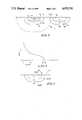
- FIG. 6is a graph of the electric field of the four layer device of FIG. 5 as a function of distance from the surface of the substrate.
- FIG. 7is a cross-sectional view at one stage of manufacture incorporating the principles of the present invention.
- FIG. 1A lateral insulated gate field effect transistor incorporating these principles is illustrated in FIG. 1.
- the drainis an N- substrate region 10 having a P body region 12 with an N+ source region 14 therein and an N+ drain contact region 16 in the drain region 10.
- a gate oxide 18 and gate 20extends along the surface over the channel portion of body region 12 between the N+ source region 14 and the drain region 10. This is a standard structure for a lateral doubly diffused insulated gate field effect transistor.
- the present inventionincorporates an increased impurity concentration N region 22 at the drain-body junction 24.
- the N-type region 22has a decreasing impurity concentration profile from the junction 24 into the drain region 10.
- the impurity concentration profiledeceases sufficiently that the region 22 is depleted under reverse biasing before critical field is reached therein.
- this regionis such that critical field is reached in the increased impurity region 22 and in the drain region 10 substantially simultaneously .
- the junction breakdownis as high as it would have been in the absence of the increased impurity concentration region 22.
- the vertical and lateral spread of the increased impurity concentration region 22assures that there is not premature critical field being reached in the added region 22 or that the series resistance would be increased in any direction.
- the current pathis created, as indicated by arrow 26, between the source region 14 across the surface of the body region 12, high impurity concentration region 22, low impurity concentration drain region 10 to drain contact region 16.
- the N increased impurity concentration region 22reduces the series resistance by providing a region of low resistance in at least part of the current flow path while the diminishing doping profile assures maintenance of a high breakdown voltage.
- the use of increased impurity concentration regions of the same conductivity type as the lower impurity regionhave been used as punch-through shields. These typically in a three layer device have protected the forward bias low breakdown junction from the depletion spread from the high voltage breakdown junction.
- the emitter-base junctionwill include a punch-through shield around the emitter having the same conductivity type as the base region but having a higher impurity concentration. This protects the emitter-base junction from the depletion spread from the reverse bias collector-base junction.
- the principle of the present inventionis also applicable to vertical doubly diffused insulated gate field effect transistors as illustrated in FIG. 2.
- the N- drain region 10is shown as being formed on the N+ buried drain region 16'. This region 10 may be an epitaxial layer.
- the body region 12, source region 14 and increased impurity concentration 22are shown formed as annuluses or rings.
- the gate oxide 18 and gate region 20are also shown formed as annuluses or rings.
- the current lines 28are shown as substantially vertical extending from the surface source region 14 down through the body regions 12, increased impurity concentration region 22, low impurity concentration drain region 10 to buried drain contact region 16'.
- the impurity concentration profile and, thus, the operation of the increased impurity concentration region 22is the same for the vertical insulated gate field effect transistor of FIG. 2 as it is for the lateral insulated gate field effect transistor of FIG. 1.
- a high voltage bipolar transistoris illustrated in FIG. 3 as including a low impurity N- concentration collector region 30 having a P base region 32 formed therein, an N+ emitter region 34 formed in the base region 32 and an N+ collector contact 36 formed in the surface of the N- collector region 30.
- An increased impurity N-type concentration region 38is formed at the PN junction 40 between the base region 32 and collector region 30.
- the impurity concentration profile of the region 38decreases from the PN junction 40 through the collector region 30.
- the impurity concentrationis selected such that the region 38 is depleted before critical field is reached therein. As in the preferred embodiments of FIGS. 1 and 2, ideally the critical field is reached simultaneously in the increased impurity concentration region 38 and the collector region 30 simultaneously.
- Current lines 42illustrate that the increased impurity region 38 reduces the collector series resistance.
- the principleis also applicable to low voltage bipolar transistors as illustrated in FIG. 4.
- the N+ contact region 36By placing the N+ contact region 36 in the increased impurity concentration region 38, the total series collector resistance is low since it does not include any of the N- collector regions 30.
- the collector contactBy placing the collector contact in the increased impurity concentration regions 38, the collector base junction cannot support as high a breakdown voltage as in FIG. 3. It should be noted that the structure of FIGS. 3 and 4 are the same except for the placement of the N+ contact region and therefore may be formed during the same process step and therefore be incorporated in a common integrated circuit.
- FIGS. 3 and 4The principles of the bipolar transistors of FIGS. 3 and 4 are also applicable to diodes. It is well known in the industry to use the base collector junction as a diode structure. Thus, the structure of FIGS. 3 and 4 could be built without emitter region 34 or the emitter 34 may be electrically inactive by not connecting it to a voltage or connecting it to the base region 32. In any application, the impurity concentration profile of region 38 is selected to deplete before critical field is reached therein. Thus, the principle is applicable to a PN junction by providing a region on the lightly doped side having a unique impurity profile.
- An N+ cathode 44 as a first layeris formed in a second layer P-type region 46 which is formed in a third layer N- region 48.
- the fourth layer or anode P-type region 50is also formed in the third layer 48.
- a first increased impurity concentration region 52is formed at the PN junction 54 between the second layer 46 and the third layer 48. This region acts to reduce the series resistance while not affecting the breakdown voltage of the reverse biased junction 54 as in the previously described embodiments.
- the four layer device of FIG. 5includes a second increased impurity concentration region 56 at the PN junction 58 between the fourth layer 50 and the third layer 48.
- the second increased impurity concentration region 56is a punch-through shield which protects the PN junction 58 from the depletion of region 54. As illustrated by the dotted line 60, the depletion of junction 54 extends towards anode 50 but is absorbed in the punch-through shield 56.
- FIG. 6illustrates the electric field along the surface of the four layer device of FIG. 5.
- the major voltage dropis in the N region 52 where X O is at the PN junction 54 and continues to X1 which is the junction between the N region 52 and the N- layer 48.
- X1is the junction between the N region 52 and the N- layer 48.
- the final rapid fall in electric fieldis in the punch-through shield 56 between X2 and X3.
- the combination of the two increased imurity concentration regions 46 and 50allows the heavily doped anode region 52 to be closer to the regions of significantly different voltage than would otherwise be the case.
- the anode or fourth layer 40may be formed as a buried layer below the first layer 44 and second layer 54.
- the punch-through shield 56would also be formed as a buried layer and it would serve the exact same function.
- the fourth layer 50 and the punch-through shield 56could be formed as buried expitaxial layers or buried diffused regions.
- a method for forming the increased impurity concentration region at the PN junction of a reverse bias junctionwould include, as illustrated in FIG. 7, forming a masking layer 62 on the surface of the N- substrate 10, 30.
- N-type impurityfor example phosphorus
- P-type impuritiesfor example boron
- the region 22, 38is formed graded because of the planar diffusion and the equal dimension of region 22, 38 extending from the P region 12, 32 is achieved by using the same mask aperture.
- a wash processmay be performed to remove it between the processing of the N and P-type impurities.
- N region 22, 38extends laterally and vertically equally distant from the P region 12, 32 and has a decreasing impurity concentration therefrom.
- the subsequent steps to form the third region of a three layer device or fourth region of a four layer deviceare well know and, thus, will not be described.
- the N- substrate 10would have an impurity concentration of 1 ⁇ 10 14 carriers per cubic centimeter
- the N increased impurity concentration region 22would have an average impurity concentration of 1 ⁇ 10 15 carriers per cubic centimeter, a peak impurity concentration of 2 ⁇ 10 15 carriers per cubic centimeter and a depth in the range of 2 to 20 microns.
- the P-type body region 12would have a surface impurity concentration of 5 ⁇ 10 16 carriers per square centimeter and a depth of 1 to 10 microns.
- the emitter, base and collector of the bipolar transistor of FIGS. 3 and 4would have the same depth and impurity concentration as corresponding regions of the DMOS devices.
- the increased impurity concentration regions 52 and 56are formed simultaneously in the same process step and the second layer 46 and the anode 58 are also formed simultaneously during the same process step.
Landscapes
- Insulated Gate Type Field-Effect Transistor (AREA)
Abstract
Description
Claims (11)
Priority Applications (1)
| Application Number | Priority Date | Filing Date | Title |
|---|---|---|---|
| US07/253,437US4975751A (en) | 1985-09-09 | 1988-10-05 | High breakdown active device structure with low series resistance |
Applications Claiming Priority (2)
| Application Number | Priority Date | Filing Date | Title |
|---|---|---|---|
| US77428285A | 1985-09-09 | 1985-09-09 | |
| US07/253,437US4975751A (en) | 1985-09-09 | 1988-10-05 | High breakdown active device structure with low series resistance |
Related Parent Applications (1)
| Application Number | Title | Priority Date | Filing Date |
|---|---|---|---|
| US77428285AContinuation | 1985-09-09 | 1985-09-09 |
Related Child Applications (1)
| Application Number | Title | Priority Date | Filing Date |
|---|---|---|---|
| US07/592,308DivisionUS5091336A (en) | 1985-09-09 | 1990-10-03 | Method of making a high breakdown active device structure with low series resistance |
Publications (1)
| Publication Number | Publication Date |
|---|---|
| US4975751Atrue US4975751A (en) | 1990-12-04 |
Family
ID=26943257
Family Applications (1)
| Application Number | Title | Priority Date | Filing Date |
|---|---|---|---|
| US07/253,437Expired - LifetimeUS4975751A (en) | 1985-09-09 | 1988-10-05 | High breakdown active device structure with low series resistance |
Country Status (1)
| Country | Link |
|---|---|
| US (1) | US4975751A (en) |
Cited By (17)
| Publication number | Priority date | Publication date | Assignee | Title |
|---|---|---|---|---|
| WO1992007384A1 (en)* | 1990-10-22 | 1992-04-30 | Harris Corporation | Piso electrostatic discharge protection device |
| EP0487937A1 (en)* | 1990-11-26 | 1992-06-03 | Motorola, Inc. | A semiconductor device having punch-through protected buried contacts and method for making the same |
| EP0735591A1 (en)* | 1995-03-31 | 1996-10-02 | Consorzio per la Ricerca sulla Microelettronica nel Mezzogiorno - CoRiMMe | Improved DMOS device structure, and related manufacturing process |
| WO1998009335A1 (en)* | 1996-08-29 | 1998-03-05 | The Whitaker Corporation | Monolithic integrated circuit including bipolar transistors having nonuniformly doped collector base junction |
| EP0837508A3 (en)* | 1996-10-18 | 1999-01-20 | Hitachi, Ltd. | Semiconductor device and electric power conversion apparatus therewith |
| US6137139A (en)* | 1999-06-03 | 2000-10-24 | Intersil Corporation | Low voltage dual-well MOS device having high ruggedness, low on-resistance, and improved body diode reverse recovery |
| EP1148555A1 (en)* | 2000-04-21 | 2001-10-24 | STMicroelectronics S.r.l. | RESURF LDMOS field-effect transistor |
| US6355971B2 (en)* | 1998-02-28 | 2002-03-12 | U.S. Philips Corporation | Semiconductor switch devices having a region with three distinct zones and their manufacture |
| WO2002001644A3 (en)* | 2000-06-23 | 2002-07-04 | Silicon Wireless Corp | Power mosfet and methods of forming and operating the same |
| US20020175351A1 (en)* | 2001-04-11 | 2002-11-28 | Baliga Bantval Jayant | Power semiconductor devices having retrograded-doped transition regions that enhance breakdown voltage characteristics and methods of forming same |
| US20020185679A1 (en)* | 2000-06-23 | 2002-12-12 | Baliga Bantval Jayant | Power semiconductor devices having linear transfer characteristics and methods of forming and operating same |
| US6552391B2 (en) | 2001-01-22 | 2003-04-22 | Fairchild Semiconductor Corporation | Low voltage dual-well trench MOS device |
| US20030091556A1 (en)* | 2000-12-04 | 2003-05-15 | Ruoslahti Erkki I. | Methods of inhibiting tumor growth and angiogenesis with anastellin |
| US20040099905A1 (en)* | 2001-04-11 | 2004-05-27 | Baliga Bantval Jayant | Power semiconductor devices having laterally extending base shielding regions that inhibit base reach-through and schottky rectifying flyback diodes |
| US20050196930A1 (en)* | 2004-03-08 | 2005-09-08 | Intersil Americas Inc. | Method of making bipolar transistors and resulting product |
| US20060124994A1 (en)* | 2004-12-15 | 2006-06-15 | Samsung Electronics Co., Ltd. | Vertical double-diffused metal oxide semiconductor (VDMOS) device incorporating reverse diode |
| EP3435419A1 (en)* | 2017-07-26 | 2019-01-30 | ams AG | Semiconductor device with single electron counting capability comprising an avalanche bipolar transistor |
Citations (13)
| Publication number | Priority date | Publication date | Assignee | Title |
|---|---|---|---|---|
| US3183128A (en)* | 1962-06-11 | 1965-05-11 | Fairchild Camera Instr Co | Method of making field-effect transistors |
| US3252062A (en)* | 1961-05-24 | 1966-05-17 | Philips Corp | Zener diode |
| US3450961A (en)* | 1966-05-26 | 1969-06-17 | Westinghouse Electric Corp | Semiconductor devices with a region having portions of differing depth and concentration |
| US3488527A (en)* | 1967-09-05 | 1970-01-06 | Fairchild Camera Instr Co | Punch-through,microwave negativeresistance device |
| US3722079A (en)* | 1970-06-05 | 1973-03-27 | Radiation Inc | Process for forming buried layers to reduce collector resistance in top contact transistors |
| US3821657A (en)* | 1972-10-25 | 1974-06-28 | Gen Electric | High frequency semiconductor amplifying devices and circuits therefor |
| US3865649A (en)* | 1972-10-16 | 1975-02-11 | Harris Intertype Corp | Fabrication of MOS devices and complementary bipolar transistor devices in a monolithic substrate |
| US3909320A (en)* | 1973-12-26 | 1975-09-30 | Signetics Corp | Method for forming MOS structure using double diffusion |
| US3911461A (en)* | 1974-11-07 | 1975-10-07 | Motorola Inc | Semiconductor device with improved reverse transient capability |
| US4242697A (en)* | 1979-03-14 | 1980-12-30 | Bell Telephone Laboratories, Incorporated | Dielectrically isolated high voltage semiconductor devices |
| US4258379A (en)* | 1978-09-25 | 1981-03-24 | Hitachi, Ltd. | IIL With in and outdiffused emitter pocket |
| US4290831A (en)* | 1980-04-18 | 1981-09-22 | Harris Corporation | Method of fabricating surface contacts for buried layer into dielectric isolated islands |
| US4366495A (en)* | 1979-08-06 | 1982-12-28 | Rca Corporation | Vertical MOSFET with reduced turn-on resistance |
- 1988
- 1988-10-05USUS07/253,437patent/US4975751A/ennot_activeExpired - Lifetime
Patent Citations (13)
| Publication number | Priority date | Publication date | Assignee | Title |
|---|---|---|---|---|
| US3252062A (en)* | 1961-05-24 | 1966-05-17 | Philips Corp | Zener diode |
| US3183128A (en)* | 1962-06-11 | 1965-05-11 | Fairchild Camera Instr Co | Method of making field-effect transistors |
| US3450961A (en)* | 1966-05-26 | 1969-06-17 | Westinghouse Electric Corp | Semiconductor devices with a region having portions of differing depth and concentration |
| US3488527A (en)* | 1967-09-05 | 1970-01-06 | Fairchild Camera Instr Co | Punch-through,microwave negativeresistance device |
| US3722079A (en)* | 1970-06-05 | 1973-03-27 | Radiation Inc | Process for forming buried layers to reduce collector resistance in top contact transistors |
| US3865649A (en)* | 1972-10-16 | 1975-02-11 | Harris Intertype Corp | Fabrication of MOS devices and complementary bipolar transistor devices in a monolithic substrate |
| US3821657A (en)* | 1972-10-25 | 1974-06-28 | Gen Electric | High frequency semiconductor amplifying devices and circuits therefor |
| US3909320A (en)* | 1973-12-26 | 1975-09-30 | Signetics Corp | Method for forming MOS structure using double diffusion |
| US3911461A (en)* | 1974-11-07 | 1975-10-07 | Motorola Inc | Semiconductor device with improved reverse transient capability |
| US4258379A (en)* | 1978-09-25 | 1981-03-24 | Hitachi, Ltd. | IIL With in and outdiffused emitter pocket |
| US4242697A (en)* | 1979-03-14 | 1980-12-30 | Bell Telephone Laboratories, Incorporated | Dielectrically isolated high voltage semiconductor devices |
| US4366495A (en)* | 1979-08-06 | 1982-12-28 | Rca Corporation | Vertical MOSFET with reduced turn-on resistance |
| US4290831A (en)* | 1980-04-18 | 1981-09-22 | Harris Corporation | Method of fabricating surface contacts for buried layer into dielectric isolated islands |
Non-Patent Citations (4)
| Title |
|---|
| Pederson, D. O., et al., Introduction to Electronic Systems, Circuits, and Devices, McGraw Hill, 1966, p. 143 173.* |
| Pederson, D. O., et al., Introduction to Electronic Systems, Circuits, and Devices, McGraw-Hill, 1966, p. 143-173. |
| Streetman, B., Solid State Electronic Devices, Prentice Hall, Inc., 1972, pp. 177 180, 155 159.* |
| Streetman, B., Solid State Electronic Devices, Prentice-Hall, Inc., 1972, pp. 177-180, 155-159. |
Cited By (36)
| Publication number | Priority date | Publication date | Assignee | Title |
|---|---|---|---|---|
| US5138413A (en)* | 1990-10-22 | 1992-08-11 | Harris Corporation | Piso electrostatic discharge protection device |
| WO1992007384A1 (en)* | 1990-10-22 | 1992-04-30 | Harris Corporation | Piso electrostatic discharge protection device |
| EP0487937A1 (en)* | 1990-11-26 | 1992-06-03 | Motorola, Inc. | A semiconductor device having punch-through protected buried contacts and method for making the same |
| US6218228B1 (en) | 1995-03-31 | 2001-04-17 | Consorzio Per La Ricerca Sulla Microelettronica Nel Mezzogiorno | DMOS device structure, and related manufacturing process |
| EP0735591A1 (en)* | 1995-03-31 | 1996-10-02 | Consorzio per la Ricerca sulla Microelettronica nel Mezzogiorno - CoRiMMe | Improved DMOS device structure, and related manufacturing process |
| US5838042A (en)* | 1995-03-31 | 1998-11-17 | Consorzio Per La Ricerca Sulla Microelettronica Nel Mezzogiorno | DMOS device structure, and related manufacturing process |
| WO1998009335A1 (en)* | 1996-08-29 | 1998-03-05 | The Whitaker Corporation | Monolithic integrated circuit including bipolar transistors having nonuniformly doped collector base junction |
| EP0837508A3 (en)* | 1996-10-18 | 1999-01-20 | Hitachi, Ltd. | Semiconductor device and electric power conversion apparatus therewith |
| US6355971B2 (en)* | 1998-02-28 | 2002-03-12 | U.S. Philips Corporation | Semiconductor switch devices having a region with three distinct zones and their manufacture |
| US6137139A (en)* | 1999-06-03 | 2000-10-24 | Intersil Corporation | Low voltage dual-well MOS device having high ruggedness, low on-resistance, and improved body diode reverse recovery |
| EP1148555A1 (en)* | 2000-04-21 | 2001-10-24 | STMicroelectronics S.r.l. | RESURF LDMOS field-effect transistor |
| WO2002001644A3 (en)* | 2000-06-23 | 2002-07-04 | Silicon Wireless Corp | Power mosfet and methods of forming and operating the same |
| US20050001268A1 (en)* | 2000-06-23 | 2005-01-06 | Baliga Bantval Jayant | Power semiconductor devices having linear transfer characteristics when regions therein are in velocity saturation modes and methods of forming and operating same |
| US6784486B2 (en) | 2000-06-23 | 2004-08-31 | Silicon Semiconductor Corporation | Vertical power devices having retrograded-doped transition regions therein |
| US20020185679A1 (en)* | 2000-06-23 | 2002-12-12 | Baliga Bantval Jayant | Power semiconductor devices having linear transfer characteristics and methods of forming and operating same |
| US6545316B1 (en) | 2000-06-23 | 2003-04-08 | Silicon Wireless Corporation | MOSFET devices having linear transfer characteristics when operating in velocity saturation mode and methods of forming and operating same |
| US20030091556A1 (en)* | 2000-12-04 | 2003-05-15 | Ruoslahti Erkki I. | Methods of inhibiting tumor growth and angiogenesis with anastellin |
| US6552391B2 (en) | 2001-01-22 | 2003-04-22 | Fairchild Semiconductor Corporation | Low voltage dual-well trench MOS device |
| US20040099905A1 (en)* | 2001-04-11 | 2004-05-27 | Baliga Bantval Jayant | Power semiconductor devices having laterally extending base shielding regions that inhibit base reach-through and schottky rectifying flyback diodes |
| US7041559B2 (en) | 2001-04-11 | 2006-05-09 | Silicon Semiconductor Corporation | Methods of forming power semiconductor devices having laterally extending base shielding regions |
| US20020177277A1 (en)* | 2001-04-11 | 2002-11-28 | Baliga Bantval Jayant | Power semiconductor devices having laterally extending base shielding regions that inhibit base reach through and methods of forming same |
| US6791143B2 (en) | 2001-04-11 | 2004-09-14 | Silicon Semiconductor Corporation | Power semiconductor devices having laterally extending base shielding regions that inhibit base reach-through |
| US6800897B2 (en) | 2001-04-11 | 2004-10-05 | Silicon Semiconductor Corporation | Integrated circuit power devices having junction barrier controlled schottky diodes therein |
| US20040232479A1 (en)* | 2001-04-11 | 2004-11-25 | Baliga Bantval Jayant | Methods of forming vertical power devices having trench-based source electrodes with sidewall source contacts |
| US20020175351A1 (en)* | 2001-04-11 | 2002-11-28 | Baliga Bantval Jayant | Power semiconductor devices having retrograded-doped transition regions that enhance breakdown voltage characteristics and methods of forming same |
| US20050032291A1 (en)* | 2001-04-11 | 2005-02-10 | Baliga Bantval Jayant | Methods of forming power semiconductor devices having laterally extending base shielding regions |
| US6781194B2 (en) | 2001-04-11 | 2004-08-24 | Silicon Semiconductor Corporation | Vertical power devices having retrograded-doped transition regions and insulated trench-based electrodes therein |
| US20050196930A1 (en)* | 2004-03-08 | 2005-09-08 | Intersil Americas Inc. | Method of making bipolar transistors and resulting product |
| US7067383B2 (en) | 2004-03-08 | 2006-06-27 | Intersil Americas, Inc. | Method of making bipolar transistors and resulting product |
| US20060199350A1 (en)* | 2004-03-08 | 2006-09-07 | Intersil Americas, Inc. | Method of Making Bipolar Transistors and Resulting Product |
| US7327012B2 (en) | 2004-03-08 | 2008-02-05 | James Douglas Beasom | Bipolar Transistor Devices |
| US20060124994A1 (en)* | 2004-12-15 | 2006-06-15 | Samsung Electronics Co., Ltd. | Vertical double-diffused metal oxide semiconductor (VDMOS) device incorporating reverse diode |
| US7417282B2 (en)* | 2004-12-15 | 2008-08-26 | Samsung Electronics, Co., Ltd. | Vertical double-diffused metal oxide semiconductor (VDMOS) device incorporating reverse diode |
| EP3435419A1 (en)* | 2017-07-26 | 2019-01-30 | ams AG | Semiconductor device with single electron counting capability comprising an avalanche bipolar transistor |
| WO2019020471A1 (en)* | 2017-07-26 | 2019-01-31 | Ams Ag | Semiconductor device with single electron counting capability comprising an avalanche bipolar transistor |
| US11322641B2 (en) | 2017-07-26 | 2022-05-03 | Ams Ag | Semiconductor device with single electron counting capability |
Similar Documents
| Publication | Publication Date | Title |
|---|---|---|
| US4975751A (en) | High breakdown active device structure with low series resistance | |
| US6707104B2 (en) | Lateral high-breakdown-voltage transistor | |
| US4760433A (en) | ESD protection transistors | |
| US8823051B2 (en) | High-voltage diodes formed in advanced power integrated circuit devices | |
| KR100305238B1 (en) | Silicon controlled rectifier for esd protection | |
| US4837606A (en) | Vertical MOSFET with reduced bipolar effects | |
| US7719086B2 (en) | Lateral insulated gate bipolar transistor having a retrograde doping profile in base region and method of manufacture thereof | |
| US4605948A (en) | Semiconductor structure for electric field distribution | |
| US4394674A (en) | Insulated gate field effect transistor | |
| US5091336A (en) | Method of making a high breakdown active device structure with low series resistance | |
| JPH037149B2 (en) | ||
| EP0810671A2 (en) | Insulated gate bipolar transistor type semiconductor device | |
| EP0621637A1 (en) | Protective diode for transistor | |
| EP0685891B1 (en) | Integrated semiconductor diode | |
| KR100397882B1 (en) | Field effect controllable semiconductor component | |
| JP2680788B2 (en) | Integrated structure active clamp device | |
| US20080265333A1 (en) | Structure and method for enhanced triple well latchup robustness | |
| JP2718907B2 (en) | PIC structure and manufacturing method thereof | |
| US4713681A (en) | Structure for high breakdown PN diode with relatively high surface doping | |
| US8022506B2 (en) | SOI device with more immunity from substrate voltage | |
| JP3522887B2 (en) | High voltage semiconductor device | |
| US5723349A (en) | Process for manufacturing a high conductivity insulated gate bipolar transistor integrater structure | |
| EP0267768A1 (en) | High voltage drifted-drain MOS transistor | |
| US4794436A (en) | High voltage drifted-drain MOS transistor | |
| US4987469A (en) | Lateral high-voltage transistor suitable for use in emitter followers |
Legal Events
| Date | Code | Title | Description |
|---|---|---|---|
| STCF | Information on status: patent grant | Free format text:PATENTED CASE | |
| FEPP | Fee payment procedure | Free format text:PAYOR NUMBER ASSIGNED (ORIGINAL EVENT CODE: ASPN); ENTITY STATUS OF PATENT OWNER: LARGE ENTITY | |
| FPAY | Fee payment | Year of fee payment:4 | |
| REMI | Maintenance fee reminder mailed | ||
| FPAY | Fee payment | Year of fee payment:8 | |
| AS | Assignment | Owner name:INTERSIL CORPORATION, FLORIDA Free format text:ASSIGNMENT OF ASSIGNORS INTEREST;ASSIGNOR:HARRIS CORPORATION;REEL/FRAME:010247/0043 Effective date:19990813 | |
| AS | Assignment | Owner name:CREDIT SUISSE FIRST BOSTON, AS COLLATERAL AGENT, N Free format text:SECURITY INTEREST;ASSIGNOR:INTERSIL CORPORATION;REEL/FRAME:010351/0410 Effective date:19990813 | |
| AS | Assignment | Owner name:INTERSIL HOLDING CORPORATION, CALIFORNIA Free format text:INTELLECTUAL PROPERTY PARTIAL RELEASE;ASSIGNOR:CREIDT SUISSE FIRST BOSTON;REEL/FRAME:011667/0166 Effective date:20010303 | |
| AS | Assignment | Owner name:FAIRCHILD SEMICONDUCTOR CORPORATION, MAINE Free format text:REASSIGNMENT OF PATENT APPLICATIONS;ASSIGNOR:INTERSIL CORPORATION;REEL/FRAME:012002/0206 Effective date:20010406 | |
| FPAY | Fee payment | Year of fee payment:12 | |
| REMI | Maintenance fee reminder mailed |