US4974166A - Processing systems with intelligent article tracking - Google Patents
Processing systems with intelligent article trackingDownload PDFInfo
- Publication number
- US4974166A US4974166AUS07/458,767US45876789AUS4974166AUS 4974166 AUS4974166 AUS 4974166AUS 45876789 AUS45876789 AUS 45876789AUS 4974166 AUS4974166 AUS 4974166A
- Authority
- US
- United States
- Prior art keywords
- processing
- data
- container
- workstation
- transportable container
- Prior art date
- Legal status (The legal status is an assumption and is not a legal conclusion. Google has not performed a legal analysis and makes no representation as to the accuracy of the status listed.)
- Expired - Lifetime
Links
Images


Classifications
- H—ELECTRICITY
- H01—ELECTRIC ELEMENTS
- H01L—SEMICONDUCTOR DEVICES NOT COVERED BY CLASS H10
- H01L21/00—Processes or apparatus adapted for the manufacture or treatment of semiconductor or solid state devices or of parts thereof
- H01L21/67—Apparatus specially adapted for handling semiconductor or electric solid state devices during manufacture or treatment thereof; Apparatus specially adapted for handling wafers during manufacture or treatment of semiconductor or electric solid state devices or components ; Apparatus not specifically provided for elsewhere
- H01L21/67005—Apparatus not specifically provided for elsewhere
- H01L21/67242—Apparatus for monitoring, sorting or marking
- H01L21/67294—Apparatus for monitoring, sorting or marking using identification means, e.g. labels on substrates or labels on containers
- G—PHYSICS
- G06—COMPUTING OR CALCULATING; COUNTING
- G06F—ELECTRIC DIGITAL DATA PROCESSING
- G06F17/00—Digital computing or data processing equipment or methods, specially adapted for specific functions
- G—PHYSICS
- G03—PHOTOGRAPHY; CINEMATOGRAPHY; ANALOGOUS TECHNIQUES USING WAVES OTHER THAN OPTICAL WAVES; ELECTROGRAPHY; HOLOGRAPHY
- G03F—PHOTOMECHANICAL PRODUCTION OF TEXTURED OR PATTERNED SURFACES, e.g. FOR PRINTING, FOR PROCESSING OF SEMICONDUCTOR DEVICES; MATERIALS THEREFOR; ORIGINALS THEREFOR; APPARATUS SPECIALLY ADAPTED THEREFOR
- G03F7/00—Photomechanical, e.g. photolithographic, production of textured or patterned surfaces, e.g. printing surfaces; Materials therefor, e.g. comprising photoresists; Apparatus specially adapted therefor
- G03F7/70—Microphotolithographic exposure; Apparatus therefor
- G03F7/70483—Information management; Active and passive control; Testing; Wafer monitoring, e.g. pattern monitoring
- G03F7/70491—Information management, e.g. software; Active and passive control, e.g. details of controlling exposure processes or exposure tool monitoring processes
- G03F7/70525—Controlling normal operating mode, e.g. matching different apparatus, remote control or prediction of failure
- G—PHYSICS
- G03—PHOTOGRAPHY; CINEMATOGRAPHY; ANALOGOUS TECHNIQUES USING WAVES OTHER THAN OPTICAL WAVES; ELECTROGRAPHY; HOLOGRAPHY
- G03F—PHOTOMECHANICAL PRODUCTION OF TEXTURED OR PATTERNED SURFACES, e.g. FOR PRINTING, FOR PROCESSING OF SEMICONDUCTOR DEVICES; MATERIALS THEREFOR; ORIGINALS THEREFOR; APPARATUS SPECIALLY ADAPTED THEREFOR
- G03F7/00—Photomechanical, e.g. photolithographic, production of textured or patterned surfaces, e.g. printing surfaces; Materials therefor, e.g. comprising photoresists; Apparatus specially adapted therefor
- G03F7/70—Microphotolithographic exposure; Apparatus therefor
- G03F7/70483—Information management; Active and passive control; Testing; Wafer monitoring, e.g. pattern monitoring
- G03F7/70491—Information management, e.g. software; Active and passive control, e.g. details of controlling exposure processes or exposure tool monitoring processes
- G03F7/70541—Tagging, i.e. hardware or software tagging of features or components, e.g. using tagging scripts or tagging identifier codes for identification of chips, shots or wafers
- G—PHYSICS
- G03—PHOTOGRAPHY; CINEMATOGRAPHY; ANALOGOUS TECHNIQUES USING WAVES OTHER THAN OPTICAL WAVES; ELECTROGRAPHY; HOLOGRAPHY
- G03F—PHOTOMECHANICAL PRODUCTION OF TEXTURED OR PATTERNED SURFACES, e.g. FOR PRINTING, FOR PROCESSING OF SEMICONDUCTOR DEVICES; MATERIALS THEREFOR; ORIGINALS THEREFOR; APPARATUS SPECIALLY ADAPTED THEREFOR
- G03F7/00—Photomechanical, e.g. photolithographic, production of textured or patterned surfaces, e.g. printing surfaces; Materials therefor, e.g. comprising photoresists; Apparatus specially adapted therefor
- G03F7/70—Microphotolithographic exposure; Apparatus therefor
- G03F7/70691—Handling of masks or workpieces
- G03F7/70733—Handling masks and workpieces, e.g. exchange of workpiece or mask, transport of workpiece or mask
- G03F7/7075—Handling workpieces outside exposure position, e.g. SMIF box
- G—PHYSICS
- G03—PHOTOGRAPHY; CINEMATOGRAPHY; ANALOGOUS TECHNIQUES USING WAVES OTHER THAN OPTICAL WAVES; ELECTROGRAPHY; HOLOGRAPHY
- G03F—PHOTOMECHANICAL PRODUCTION OF TEXTURED OR PATTERNED SURFACES, e.g. FOR PRINTING, FOR PROCESSING OF SEMICONDUCTOR DEVICES; MATERIALS THEREFOR; ORIGINALS THEREFOR; APPARATUS SPECIALLY ADAPTED THEREFOR
- G03F7/00—Photomechanical, e.g. photolithographic, production of textured or patterned surfaces, e.g. printing surfaces; Materials therefor, e.g. comprising photoresists; Apparatus specially adapted therefor
- G03F7/70—Microphotolithographic exposure; Apparatus therefor
- G03F7/708—Construction of apparatus, e.g. environment aspects, hygiene aspects or materials
- G03F7/70991—Connection with other apparatus, e.g. multiple exposure stations, particular arrangement of exposure apparatus and pre-exposure and/or post-exposure apparatus; Shared apparatus, e.g. having shared radiation source, shared mask or workpiece stage, shared base-plate; Utilities, e.g. cable, pipe or wireless arrangements for data, power, fluids or vacuum
- G—PHYSICS
- G05—CONTROLLING; REGULATING
- G05B—CONTROL OR REGULATING SYSTEMS IN GENERAL; FUNCTIONAL ELEMENTS OF SUCH SYSTEMS; MONITORING OR TESTING ARRANGEMENTS FOR SUCH SYSTEMS OR ELEMENTS
- G05B19/00—Programme-control systems
- G05B19/02—Programme-control systems electric
- G05B19/418—Total factory control, i.e. centrally controlling a plurality of machines, e.g. direct or distributed numerical control [DNC], flexible manufacturing systems [FMS], integrated manufacturing systems [IMS] or computer integrated manufacturing [CIM]
- G05B19/4183—Total factory control, i.e. centrally controlling a plurality of machines, e.g. direct or distributed numerical control [DNC], flexible manufacturing systems [FMS], integrated manufacturing systems [IMS] or computer integrated manufacturing [CIM] characterised by data acquisition, e.g. workpiece identification
- H—ELECTRICITY
- H01—ELECTRIC ELEMENTS
- H01L—SEMICONDUCTOR DEVICES NOT COVERED BY CLASS H10
- H01L21/00—Processes or apparatus adapted for the manufacture or treatment of semiconductor or solid state devices or of parts thereof
- H01L21/67—Apparatus specially adapted for handling semiconductor or electric solid state devices during manufacture or treatment thereof; Apparatus specially adapted for handling wafers during manufacture or treatment of semiconductor or electric solid state devices or components ; Apparatus not specifically provided for elsewhere
- H01L21/67005—Apparatus not specifically provided for elsewhere
- H01L21/67242—Apparatus for monitoring, sorting or marking
- H01L21/67276—Production flow monitoring, e.g. for increasing throughput
- G—PHYSICS
- G05—CONTROLLING; REGULATING
- G05B—CONTROL OR REGULATING SYSTEMS IN GENERAL; FUNCTIONAL ELEMENTS OF SUCH SYSTEMS; MONITORING OR TESTING ARRANGEMENTS FOR SUCH SYSTEMS OR ELEMENTS
- G05B2219/00—Program-control systems
- G05B2219/30—Nc systems
- G05B2219/31—From computer integrated manufacturing till monitoring
- G05B2219/31002—Computer controlled agv conveys workpieces between buffer and cell
- G—PHYSICS
- G05—CONTROLLING; REGULATING
- G05B—CONTROL OR REGULATING SYSTEMS IN GENERAL; FUNCTIONAL ELEMENTS OF SUCH SYSTEMS; MONITORING OR TESTING ARRANGEMENTS FOR SUCH SYSTEMS OR ELEMENTS
- G05B2219/00—Program-control systems
- G05B2219/30—Nc systems
- G05B2219/31—From computer integrated manufacturing till monitoring
- G05B2219/31286—Detect position of articles and equipment by receivers, identify objects by code
- G—PHYSICS
- G05—CONTROLLING; REGULATING
- G05B—CONTROL OR REGULATING SYSTEMS IN GENERAL; FUNCTIONAL ELEMENTS OF SUCH SYSTEMS; MONITORING OR TESTING ARRANGEMENTS FOR SUCH SYSTEMS OR ELEMENTS
- G05B2219/00—Program-control systems
- G05B2219/30—Nc systems
- G05B2219/31—From computer integrated manufacturing till monitoring
- G05B2219/31323—Database for CIM
- G—PHYSICS
- G05—CONTROLLING; REGULATING
- G05B—CONTROL OR REGULATING SYSTEMS IN GENERAL; FUNCTIONAL ELEMENTS OF SUCH SYSTEMS; MONITORING OR TESTING ARRANGEMENTS FOR SUCH SYSTEMS OR ELEMENTS
- G05B2219/00—Program-control systems
- G05B2219/30—Nc systems
- G05B2219/31—From computer integrated manufacturing till monitoring
- G05B2219/31432—Keep track of conveyed workpiece, batch, tool, conditions of stations, cells
- Y—GENERAL TAGGING OF NEW TECHNOLOGICAL DEVELOPMENTS; GENERAL TAGGING OF CROSS-SECTIONAL TECHNOLOGIES SPANNING OVER SEVERAL SECTIONS OF THE IPC; TECHNICAL SUBJECTS COVERED BY FORMER USPC CROSS-REFERENCE ART COLLECTIONS [XRACs] AND DIGESTS
- Y02—TECHNOLOGIES OR APPLICATIONS FOR MITIGATION OR ADAPTATION AGAINST CLIMATE CHANGE
- Y02P—CLIMATE CHANGE MITIGATION TECHNOLOGIES IN THE PRODUCTION OR PROCESSING OF GOODS
- Y02P90/00—Enabling technologies with a potential contribution to greenhouse gas [GHG] emissions mitigation
- Y02P90/02—Total factory control, e.g. smart factories, flexible manufacturing systems [FMS] or integrated manufacturing systems [IMS]
Definitions
- the present inventionrelates to standardized mechanical interface systems for reducing particle contamination of semiconductor wafers during semiconductor processing. More particularly, the present invention relates to an apparatus for information processing in standard mechanical interface systems.
- a standardized mechanical interface (SMIF) systemhas been proposed to reduce particle contamination by significantly reducing particle fluxes onto wafers. This end is accomplished by mechanically insuring that during transport, storage and processing of the wafers, the gaseous media (such as air or nitrogen) surrounding the wafers is essentially stationary relative to the wafers and by inSuring that particles from the outside environment do not enter the immediate internal wafer environment.
- the gaseous mediasuch as air or nitrogen
- the SMIF conceptis based on the realization that a small volume of still, particle free air, with no internal source of particles, is the cleanest possible environment for wafers. Further details of one proposed system are described in the article "SMlF: A Technology for Wafer Cassette Transfer and VLSI Manufacturing", by Mihir Parikh and Ulrich Kaemph, Solid State Technology, July 1984, pp. 111-115, and the above cross-referenced applications.
- a SMIF systemhas three main components, namely, (1) minimum volume, dust proof transportable containers or boxes are used for storing and transporting wafer cassettes; (2) canopies are placed over the cassette ports of processing equipment so that the environments inside the boxes and the canopies become miniature clean spaces; and (3) doors on the boxes are designed to mate with doors on the interface ports on the equipment canopies and two doors are open simultaneously so that particles which may have been on the external door surfaces are trapped (sandwiched) between the doors.
- a boxis placed at the interface port on top of the canopy at a desired processing station; latches release the boxed door and the interface port door simultaneously.
- a mechanical elevatorlowers the two doors with the cassette riding on top into the canopy covered space.
- a manipulatorpicks up the cassette and places it into the cassette port/elevator of the equipment. After processing, the reverse operation takes place.
- clean roomsare established in which through filtering and other techniques attempts are made to remove particles which may cause contamination on semiconductor wafer surfaces.
- the SMIF conceptis one way which has come under consideration for improving the processing environment over that available in clean rooms.
- the proposed SMlF systemsinvolve transporting cassettes of wafers from processing station to processing station inside the boxes.
- a given processing stationmay be located long distances from the preceding station.
- the processingmay be complex, involving a large number of steps different processing times, requiring the boxes including wafer cassettes to be stored between processing stations.
- there is a need to identify the boxes containing wafersso that information about the wafers within the boxes can be processed.
- the proposed SMIF systemshave not been fully satisfactory.
- the SMIF systems which have been proposedinclude boxes which may be marked with "OCR" or bar codes. This sort of proposed marking will identify the particular box, however, the user is unable to effectively include information with the box concerning the wafers within the box. Further, external markings of this nature do not serve to control physical access to the wafers in the box. Accordingly, there is a need for improved apparatus for information processing in SMIF systems.
- an object of the present inventionto provide a system for transporting and storing articles which provides improved tracking of the articles.
- a further object of the present inventionis to provide a system which centrally tracks articles undergoing processing and which centrally stores data regarding articles undergoing processing at a variety of locations.
- Another object of the present inventionis to provide a system which centrally controls the processing of articles being processed at a plurality of workstations so that the proper process steps and are performed in the proper sequence.
- Another object of the present inventionis to provide a system for processing articles which reduces or eliminates human decision making regarding the process to be performed at the point of processing.
- a systemin which a plurality of containers are each provided with data storage and a communication link for reading and updating the stored data.
- a plurality of workstationseach have a communication link which reads the data stored by the container and confirms that the articles in the container have arrived at the proper location.
- the workstationalso reports that the articles have arrived and the status of the articles to a central data processor.
- the central data processordownloads processing information and the workstation then removes that articles from the container and processes the articles. After processing the workstation reports to the central data processor and updates the information stored by the container.
- a system for performing a series of processing steps for an article in accordance with the present inventioncomprises:
- a transportable container for the articleincluding:
- first interface meansfor controlling access to the article in said transportable container
- container data processing meansfor receiving, storing and transmitting data relating to the identity and processing history of the article
- second interface meansprovided at each workstation, for interfacing with said first interface means
- workstation data processing meansprovided at each workstation, for receiving data from and transmitting data to said container data processing means, for processing the data received from said container data processing means, and for controlling said first and second interface means to permit access to the article in said transportable container based on a comparison of the processing history of the article and the identity of the workstation;
- central data processing meansfor receiving data from and transmitting data to each of said container and workstation data processing means and for processing data received from each of said container and workstation data processing means.
- FIG. 1shows a perspective view of a SMIF system positioned adjacent processing equipment.
- FIG. 2is a schematic representation of a SMIF system employing the present invention.
- FIG. 3A and 3Bare circuit diagrams of one embodiment of the present invention.
- FIG. 4is an alternative embodiment of an apparatus according to the present invention.
- FIG. 5is a schematic diagram of a power supply according to the present invention.
- FIG. 6is a schematic representation of the mounting relationship of apparatus according to the present invention.
- FIG. 7is a block diagram of a system included on the transportable container in one embodiment of the present invention.
- FIG. 8is a chart used in explanation of part of the circuit of FIG. 5.
- FIG. 9A, 9B and 9Cconstitute a flow chart used in the explanation of the processing system in accordance with the present invention.
- FIG. 10is an alternative flow chart for substitution for a portion of the flow chart of FIG. 9.
- FIG. 11is a flow chart used in the explanation of the processing system in accordance with the present invention.
- FIG. 12is a perspective view of a tray and transportable container of the inventory management system in accordance with the present invention.
- FIG. 13is a block diagram of an inventory management system in accordance with the invention.
- FIG. 14is a block diagram of one application of a system in accordance with the present invention.
- a semiconductor wafer processing station 100is shown.
- a given semiconductor manufacturing processmay include any number of processing stations such as the station 100 shown in FIG. 1.
- the stationsare manufactured to handle processing steps such as the application of photo resist materials, the alignment of masks for exposing photo resist materials, the deposition of materials on semiconductor wafers, and so forth.
- FIG. 1shows a transportable container 10 for semiconductor wafers, or other articles to be processed, mounted on the processing station 100.
- the transportable container 10is removeably engaged on the canopy 30 of the processing station 100 by a means 60 for engaging described with reference to FIG. 2.
- the transportable container 10is adapted for containing a cartridge 31 for holding a plurality of semiconductor wafers 32.
- the cartridge 31is lowered into the processing station 100 without exposure to outside air.
- an intelligent data card 40is mounted on the transportable container 10.
- data cardrefers to the portion of the present invention mounted on the transportable container 10, and at a minimum includes data storage means as described below.
- mounted on the processing station 100is a means 50 for communication with an electronic card 40 on a transportable container 10 engaged on the processing station 100.
- the means 50 for communicating with the data card 40is connected to a data processor 20 on the processing station 100.
- the data processor 20may include a display 21 such as an LED or liquid crystal display.
- the data processor 20may include a keyboard 22 for inputting data regarding for instance the control of the process.
- an operatorwill carrier the transportable container 10 from a first processing station 100 to a second processing station 100 with the data card 40 attached to the container 10.
- the data stored in the data card 40is communicated to the means 50 on the processing station 100 for communicating with the data card 40 when the transportable container 10 is engaged.
- the data from the data card 40 on the transportable container 10is communicated through the means 50 to the data processor 20.
- the data processor 20may also communicate to the data card 40 through the means 50.
- FIG. 2illustrates schematically the transportable container 10 engaged on the canopy 30 of a processing station.
- An engaging means 60 for engaging the transportable container 10 on the canopy 30 of the processing stationis shown.
- the engaging means 60includes a guide 61 on the canopy. Also, a tab 62 is formed on the transportable container 10.
- the port 70 on the canopy 30 through which the cartridge of semiconductor wafers is loweredis aligned with the transportable container 10.
- the data card 40is mounted on the transportable container 10 along at least one side of the transportable container 10.
- the communicating means 50is mounted adjacent the engaging means 60 in relationship with the card 40.
- the communicating means 50is connected over communicating line 51 to the process controller 20 on the processing station 100.
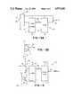
- FIG. 3Aillustrates a circuit for mounting on the data card 40 in one embodiment of the present invention.
- FIG. 3Billustrates a communication means 50 for receiving data from the card 40 as shown in FIG. 3A.
- the circuit of FIG. 3Aincludes a timer/counter 41 and a storage means 42 such as a "PROM" or other stable storage device.
- the timer/counter 41is connected to the storage means 42 across a communication bus 43.
- the timer/counterwhen power is applied, generates addresses in sequence to the storage means 41 which outputs data through the light emitting diode 44 or other optical transmission means.
- the communicating means 50 of FIG. 3Bincludes a photosensitive transistor 52 or other photo detector which responds to the data transmitted by the light emitting diode 44 to generate a signal across the control line 51 for communication with process control on the processing station 100.
- a photosensitive transistor 52 or other photo detectorwhich responds to the data transmitted by the light emitting diode 44 to generate a signal across the control line 51 for communication with process control on the processing station 100.
- the data card 40includes a power supply 45, such as a battery.
- the power supplywill be applied to the timer/counter by a switch 46 which is engaged only when the transportable container 10 is fully engaged on the engaging means 60.
- FIG. 4An alternative embodiment for a circuit on the data card 40 is shown in FIG. 4.
- the embodiment of FIG. 4includes a microcomputer 101 or other data processing means and a static memory device such as a RAM 102.
- the microcomputer 101communicates with the memory device 102 across the bus 103.
- the microcomputer 101communicates with a transmitter 104 such as the light emitting diode 105.
- the microcomputer 101communicates with a receiver 106 such as the photosensitive transistor 107.
- the microcomputerreceives power from power supply (described below) at +5 volts along line 108.
- the memory device 102receives power from a battery along line 109.
- the storage device 102likewise receives an enable signal on line 110 when the power supply supplying power to the microcomputer 101 is in operation.
- the generation of the power supply voltage on line 108, the battery voltage on line 109 and the enable signal on line 110is accomplished by the circuit shown in FIG. 5.
- FIG. 5shows a power supply 120 for mounting on the data card 40 used in conjunction with the circuit shown in FIG. 4.
- the power supply 120is adapted to receive power through a transformer coupling device 121, when the transportable container 10 is engaged by the engaging means 60 on the processing station 100.
- An AC signalis received from transformer coupling means 121 and converted to DC in an AD to DC converter 122, such as the bridge shown in FIG. 5.
- a voltage regulator 123may be included to provide a stable voltage for the operation of the components on the data card 40.
- the output of the voltage regulator 123is supplied as the power supply voltage to the microcomputer 101 across line 108 in the embodiment of FIG. 4.
- a battery 125is included on the data card 40.
- the battery voltageis slightly less than the output of the voltage regulator 123 on line 108. It is connected through the Shottley diode 126 to the node 127 which is likewise connect through a Shottley diode 128 to the power supply output on line 108. Node 127 is supplied as the battery voltage to the storage device 102 on line 109.
- the memory enable signal(MENABLE) operates to enable the memory device 102 only when the power from the transformer coupled power 121 is turned on.
- the memory enable circuitis generated as it will be described with reference to FIG. 8.
- the rectifying optocoupler 141is a means for generating voltage on line 143 from the power supply such as battery 125 when the power from the transformer coupling device is off.
- the power from the transformer coupling deviceturns on as indicated by line 200 of FIG. 8 at point 201
- output on line 143tends to drop which can be seen at point 301 of line 300 on FIG. 8.
- the speed at which the voltage on line 143, MENABLEcan drop as determined by the time constant set by R1 and C1.
- the power on line 108will reach the voltage necessary to drive the microcomputer 101 before the enable signal on line 110 reaches a level to enable the memory device 102. This prevents causing disruption of the data stored in the memory device before the power is completely up in the data card 40.
- the rectifying optocoupler 141will supply a charging current across line 143 which will rapidly charge the capacitor C1 as can be seen at point 302 on line FIG. 8.
- the static RAMwill be disabled very rapidly when power is turned off from the transformer coupling device 121.
- a variety of other circuits for protecting the data stored in the memory device 102can be devised as suits the particular embodiment of the data card 40 chosen by the user.
- FIG. 6shows one configuration for mounting the data card 40, such as the one described with reference to FIGS. 4 and 5, in communication with the communication means 50 for receiving the data from the data card 40 and transmitting data to the data card 40.
- the data card 40 and the communicating means 50are aligned for communication.
- a transformer coupling device 21is mounted on the data card 40.
- a mate transformer coupling device 131is mounted on the communicating means 50.
- FIG. 6schematically are the transmitting means 104 and the receiving means 106 on the card 40.
- Mounted adjacent the transmitting means 104 on the communicating means 50 when the transportable container 10 is fully engagedis a mate receiving means 134 for receiving the data from the data card 40.
- a transmitting means 136is mounted on the communicating means 50 so that it is adjacent the receiving means 106 on the transportable container 10 when the transportable container 10 is fully engaged on the engaging means 60.
- the communicating means 50communicates across the communication line 51 with the data processing means 20 on the processing station 100.
- FIG. 7A preferred embodiment of the circuit mounted on the data card 40 is shown in FIG. 7.
- the data card 40 shown schematically in FIG. 7includes a data processing system 151 in communication across a bus 152 with a plurality 153 of input/output devices.
- the data processing systemincludes a CPU 154, a non-volatile memory device such as a ROM 155, a random access memory device 156 for reading and writing data, and a power supply 157 such as the power supply shown in FIG. 5.
- the plurality of input/output devicesinclude any one of the following devices.
- a display 160such as an LED or liquid crystal display, may be mounted on the data card 40 for providing data to an operator.
- a keyboard 161may be mounted on the data card 40 with the transportable container 10 so that an operator may control data stored within the data card 40.
- a sensor device 162may be included on the data card 40 which communicates with a plurality of sensors on the transportable container 10. These sensors may provide information regarding conditions, such as engagement or disengagement of the transportable container 10 with an engaging means 60, opening or closing of the port in the transportable container 10 for allowing access to the articles stored within a container or other conditions. Further, a sensor may be included which indicates whether a retaining device has engaged the articles stored in the container. Many other sensors may be included depending on the particular processing steps being carried out and the characteristics of articles being transported in the transportable container 10.
- the plurality of input/output devices 153includes a transmitter 163 and a receiver 164 such as the light emitting diode 44 and photosensitive transistor 52 discussed with reference to FIGS. 4 and 6.
- the transmitter 163 and receiver 164may be of other varieties of phototransistors and photodetectors as suited to the particular use required. Further, the transmitter and receiver may be comprised of a magnetic tape and a magnetic reading head. Other acoustic, inductive or optical means of accomplishing data communication between the electronic data card 40 and the communication means 50 may be implemented as suits the particular needs of the device.
- the data card 40may include a real time clock 165 for generating data regarding real time. Data from the clock 165 may be useful by the processing stations in determining parameters for processing and the like. Also, the clock 165 may be used for determining length of storage time for the articles contained in the transportable container 10.
- the transportable container 10 with the data card 40 attached to itcan be used in conjunction with a plurality of work stations, such as the work station 100 illustrated in FIG. 1, to form a novel distributed processing system.
- a distributed processing systemis used to fabricate semiconductor integrated circuits.
- the fabrication of semiconductor integrated circuitstypically involves the processing of semiconductor wafers using a variety of discrete processing operations using a corresponding variety of work stations.
- the processing operations and corresponding work stations involved in the fabrication of a semiconductor integrated circuit from a semiconductor wafermight include the following operations and work stations
- a resistis applied to the wafer at a first work station.
- the thickness of the resistis measured at a second work station.
- a circuit patternis exposed onto the resist at a third work station.
- the circuit patternis developed at a fourth work station.
- the width of one or more circuit tracesare measured at a fifth work station.
- Etching of the exposed resistis performed at a sixth work station.
- each batchmay be enclosed within a different transportable container 10 or group of containers each with its own associated card 40.
- different batches of wafersmay undergo different operations at different work stations so as to ultimately produce different types of semiconductor integrated circuits.
- different batches of semiconductor wafersmay use the same work stations, but may be processed somewhat differently by the work stations as to ultimately produce different types of semiconductor integrated circuits.
- the resists of two batches of wafersboth might be etched at the sixth work station, but one batch might be etched for a longer period of time than the other.
- the nature of the processing operations to be performed in the course of fabricating integrated circuits from a batch of wafersmay depend upon the outcome of earlier processing steps.
- the step of etching the exposed resist at the sixth work stationmay have an etch time which depends upon the width of the one or more circuit traces measured at the fifth work station. Therefore, the outcome of the circuit trace measurement is used to determine the etch time.
- the work station 100is merely representative of a variety of work stations which can form part of a processing system in accordance with the present invention.
- the processing systemwill be described with reference to the work station 100 shown in FIG. 1, it will be appreciated that the actual processing system includes a plurality of work stations for performing a variety of processing operations such as those discussed above: applying a resist, measuring resist thickness, exposing the resist, measuring the width of circuit traces, and etching the resist.
- local 20coupled to the local control, processor 20 (hereinafter "local" 20) is a local transfer control processor 300 and a local operation control processor 302.
- the local 20is mounted on the work station 100 in electronic communication with the means 50 which serves as a two-way communication means with the data card 40.
- the microcomputer 101 of the data card 40can engage in two-way communication, through transmitter 104 and receiver 106, with means 50.
- the local 20is in electronic communication with local transfer control processor 300 and the local operation control processor 302.
- the local transfer control processor 300controls the operation of transfer means 304 which include arms 306 for transferring a cartridge 31 containing wafers 32 between the work station 100 and the transportable container 40.
- transfer means 304include arms 306 for transferring a cartridge 31 containing wafers 32 between the work station 100 and the transportable container 40.
- One embodiment of the preferred transfer means 304is described in U.S. Pat. No. 4,676,709, entitled “LONG ARM MANIPULATOR FOR SEALED STANDARD INTERFACE APPARATUS".
- An alternative embodiment of the transfer means 304is described in U.S. Pat. No. 4,674,936, entitled "SHORT ARM MANIPULATOR FOR SEALED STANDARD MECHANICAL INTERFACE APPARATUS". These two Patents are incorporated herein by this reference.
- the local operation control processor 302controls the operation of the work station 100.
- work station 100is shown for purposes of example only. Any number of a variety of different types of work stations performing a corresponding variety of processing operations can be included in the processing system.
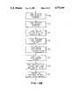
- FIGS. 9 and 10illustrate the novel distributed control aspects of the system. Distributed control is an important feature of the system of the present invention which must be flexible enough to efficiently select among a variety of processing steps and work stations.
- a transportable container 10 with its attached data card 40is transported to a work station, for example, by a human operator.
- the local 20queries the data card 40 as to whether it is ready to exchange digital information, step 404.
- the data card 40responds with a digital message generated by its microcomputers 101 (see FIG. 4) that it is set to exchange digital information, step 406.
- the local 20instructs the data card 40 to report its status, step 408.
- the microcomputer 101 of the data card 40performs a self-test, step 410.
- the self-testmay include a test to determine whether the card's battery 125 and RAM 102 are in proper working order,. If the self-test determines that the card is not in proper working order, then the microcomputer 101 causes a signal to appear on the card display 21 indicating that the card 40 may not be operating properly, step 411, and digital communication between card 40 and the local 20 typically stops. If, however, the self-test shows the card 40 to be operating properly, then the card 40 reports that the procedure may continue, step 412.
- the local 20requests that the card 40 identify itself and provide the current processing data, step 414.
- the card 40provides an identifying code.
- the cardmight also identify the lot number of the semiconductor wafers to be processed as well as the identity of the work station which is to perform the next processing step and a specification of what processing step is to be performed next, step 416.
- the next processing stepmight be the exposing of a circuit pattern onto a resist at the third work station.
- the local 20determines whether the container 10 with its contents and its card 40 is at the correct work station to perform the next processing step, step 418.
- step 420If it is not, then it informs the data card 40 which reports via display 21 that the container 10 is at the wrong work station, step 420, and typically digital communication between the card 40 and the local 20 stops. If the local 20 determines that the card 40 is at the correct work station, then digital communication continues between the card 40 and the local 20.
- the local 20responds by instructing the local transfer control processor 300 to cause the transfer of articles to be processed from the transportable container 10 to the work station 100, step 422.
- the local transfer control processor 300For example, in semiconductor integrated circuit fabrication, a cartridge 31 containing wafers 32 to be processed is lowered from the container 10 to the work station 100 via arms 306.
- the local 20instructs the local operation control processor 302 to initiate the processing operation, step 424.
- the processing operation to be performed by the work stationmight be to expose a circuit pattern onto a resist applied to a semiconductor wafer.
- the local 20informs the card that the transfer has been completed and that the processing operation has been commenced, step 426.
- the local 20composes a first history record identifying the work station and indicating that the transfer has occurred and that the processing operation was commenced, step 428.
- the local 20communicates the first history record to the card 40, step 430.
- the card 40stores first history record, step 432.
- the local 20instructs the card 40 to date and time stamp the first history record; using its microcomputer 101 and real-time clock 165 (FIG. 7); the card 40 complies with the instruction and records a date and time record for the first history record, step 434.
- the local operation control processor 302Upon completion of the processing operation, the local operation control processor 302 informs the local 20 of its completion, step 436.
- the local 20instructs the local transfer control processor 300 to imitate a transfer of the articles processed, the semiconductor wafers 32 for example, from the work station 100 back to the transportable container 10, step 438.
- the localcomposes a second history record, step 440.
- the second history recordfor example, provides a record of the operation of exposing a circuit pattern onto a resist applied to a semiconductor wafer.
- the local 20communicates the second history record to the card 40, step 442, and instructs the card 40 to date, time stamp and store the second history record, step 444.
- the local 20instructs the card 40 to advance to the next processing step, step 446.
- the card 40prepares for the next processing step, step 448, for example by changing the identity of the work station and process to be identified in step 416 at the next work station.
- the card 40causes its display 21 to identify for the operator the next work station to be visited by the transportable container, step 450.
- step 406the card 40 itself initiates and performs the self test, step 500, described above with respect to step 410. If the card 40 determines that it is not operating properly then it causes its display 21 to report its inoperability, step 502, and communication with the local 20 typically stops. On the other hand, if the card 40 determines that it is operating properly, then the card 40 requests that the local 20 report its identity, step 504. In response, the local 20 identifies itself to the card 40, step 506. The card 40 then determines whether it is the correct work station.
- step 508If it is not, it causes the display 21 to display an appropriate message, step 508, and communication with the local 20 typically stops. If the card 40 determines that it is in fact at the correct work station, then the card 40 instructs the local 20 to initiate the first material transfer, step 510.
- step 600represents the storage of the formula.
- the formulafor example, might be: K+A (width specified--width measured) +B (resist thickness). Where K, A and B are constant values, and the "width specified” refers to the specified width of a circuit trace, and “width measured” refers to the measure width of the circuit trace, and "resist thickness” is the measured thickness of a resist applied to a semiconductor wafer.
- the first processing stepis to apply a resist to semiconductor wafers being processed, step 602.
- This stepfor example, is performed at a first work station.
- the thickness of the resistis measured at a second work station, step 604, and the measured thickness is stored in the card's RAM 102, step 606.
- a circuit patternis exposed onto the resist at a third work station, step 608.
- the circuit patternis developed at a fourth work station, step 610.
- the width of one or more circuit tracesare measured at a fifth work station, step 612, and the measured width is stored in the card's RAM 102, step 614.
- the card 40using its microcomputer 101, calculates the etch time, step 616, using the formula stored in step 600 and the measurements stored in steps 606 and 614.
- the exposed resistis etched for the calculated etch time, step 618.
- the card 40advantageously can be used as part of a distributed processing system which does not require centralized control. Instead, a card 40 associated with a transportable container 10 containing articles to be processed can store processing data pertaining to the particular articles, and can perform calculations necessary to properly process the articles.
- the present inventionalso provides a novel inventory management system which advantageously can monitor the status of articles, such as semiconductor wafers for example, between processing operations.
- a tray 630including a recessed region 632 sized to receive a transportable container 10 having a data card 40 mounted on it as shown.
- the tray 630includes a two-way communication means 50-1 like the two-way communication means 50 described above and mounted on the work station 100.
- the base portion 636 of the transportable container 10can fit snugly within the recessed region 632.
- the card 40is aligned with the two-way communication means 50-1 such that the card 40 and the means 50-1 can engage in two-way communication with each other.
- FIG. 13there is shown in block diagram form an inventory management system 637 which includes a plurality of trays divided into respective qroups of trays 630-1 through 630-N. Each respective individual tray is like that described with reference to FIG. 12. Each tray in the respective groups of trays 630-1 through 630-N is coupled by a respective control line 639-1 through 639-N to a multiplexer circuit 640-1 through 640-N. The respective multiplexers 640-1 through 640-N are coupled via control line 642, which for example can be an RS232 C line, to a storage control processor 644.
- control line 642which for example can be an RS232 C line
- the storage control processor 644comprises an IBM compatible personal computer.
- the multiplexers 630-1 through 630-Nare coupled to one another in a daisy chain such that signals propagated along control line 642 proceed in a serial fashion from one multiplexer circuit to another.
- Only two groups of trays 630-1 and 630-Nare shown together, with two associated multiplexer circuits 640-l through 640-N, it will be appreciated that a plurality of groups of trays and a corresponding plurality of groups of multiplexers can be included in the inventory management system 637.
- a plurality of transportable containers 10can be placed into the respective trays 630-1 through 630-N of the inventory management system 637.
- An operatorcan use the storage control processor to ascertain, for example, the processing status of the contents of any container 10 received within any of the trays of the system 637.
- the storage control processor 644instructs the respective multiplexer circuit (not shown) coupled to that tray 630 to select that tray 630 and to couple it to the processor 644.
- the storage control processor 644sends digital signals to the selected tray 630 which cause two-way communication between the tray-mounted two-Way communication means 50-1 and the card 40.
- the storage control processor 644can ascertain the contents of the container 10, the processing steps already performed on those contents and what processing steps are scheduled to be performed in the future.
- the storage control processor 644can be used to reprogram the microcomputer 101 of the card 40, for example, so as to modify processing instructions stored in the card's RAM 102 or to update or correct its real time clock.
- the present inventory management system 637advantageously can distribute, for example, the task of maintaining a history of the processing steps and a schedule of future processing steps for the articles within respective transportable containers 10. Consequently, the storage control processor 644 is free from maintaining and managing such information.
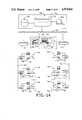
- FIG. 14One example of a material tracking system, known as a SMART-Traveler System (STS), in accordance with the present invention will be provided with reference to FIG. 14.
- the system shown in FIG. 14includes a plurality of work centers 700 n (only one work center is illustrated) and a control center 701.
- the systemis known as a SMART system because of the system's ability to track each article being processed and to centrally control the processing of each article.
- the data card 40(also known as a SMART-Tag) is the foundation of the STS.
- a data card 40is attached to each material container and carries all the information pertaining to the material inside the container 10 to which the data card is attached.
- Each data card 40has 8 kilobytes of RAM 156; a two-way infrared communications system; a battery with a life sufficient for more than one year of continuous operation; a 16 character liquid crystal display 160; an on-board microprocessor 154; and ROM 155 for storing software.
- the software stored in ROM 155includes programming for providing the data card 40 with the capability of communicating with external devices using the infrared communications system. Error-free communication is accomplished using handshakes and a double checksum error detection method. When a transmission error is detected, the communication is repeated.
- a local data processor(known as a SMART-Arm Master (SAM)) 704 is responsible for checking the data card 40 attached to each material carrier 10 to assure that the correct material is processed through the correct process steps.
- SAMSMART-Arm Master
- the SAM 704verifies that the material has come to the proper station 702. If material is not at the proper station, it is not loaded into the processing equipment 706. Once the material is loaded into the processing equipment 706, the date and time of occurrence is reported to a control center 701. A similar message is recorded when the processing is complete. Then the next sequence step information is displayed on the data card 40.
- SAM 704communicates with an automatic loading unit (ALU) 707, such as the transfer means 304 discussed above, provided at each workstation 702 via communications link 708.
- a configurable communication link 710may also be established between a SAM 704 and the processing equipment 706 to allow recipe information can be transferred directly to the processing equipment 706.
- process parameter data generated by processing equipment 706may be collected by the SAM 704 and transferred to control center 701.
- the communication between each SAM 704 and ALU 707 and processing equipment 704is SECS 1 and SECS II protocol by RS-232-C communications at 9600 BAUD.
- SMART-Storage Areas (SSAs) 740are located at each work center 700. When not undergoing processing, wafers are stored in the SSA 740 in containers 10 with data cards 40 attached. When containers 10 are brought to a SSA 740, they are placed in storage trays 630. Each storage tray 630 is connected to a storage control processor 644 via an RS-232 based communications link 746 so that the data card 40 may communicate with the storage control processor 644.
- the storage control processor 644is, for example, an IBM compatible personal computer, which monitors all material in storage, keeps a back-up copy of the data card 40 data, provides a user interface for updating data card 40 whenever a change affects a lot (for example, lot arrival, lot data change on a waiting lot), and updates the SSA 740 database maintained by storage control processor 644 and the control center 701 database.
- the program executed by storage control processor 644offers a menu-driven user interface. Most of the commands can be accessed through the use of a light pen 750 without the necessity of the keYboard. All of the features are also accessible through a keyboard.
- Control center 701provides overall facility and workcenter control and includes a central data processor (CDP) 720 which has a CPU 721, a data storage device 722, and a terminal 723 for operator interface.
- CPU 721is a VAX computer manufactured by Digital Equipment Corporation.
- the VAX computermay be configured as the PROMIS Version 4.3 central facility host system available from Promis Systems Corporation or the COMETS centralized facility host system available from Consilium.
- a networkprovides connections between CDP 720 and all other components of the STS System.
- the networkcontains three levels of communication, i.e., an Ethernet based LAN 760, an RS-485 base LANs 762, and RS-232 based communications links.
- the Ethernet LANmay be, for example, DECNET, a proprietary network of Digital Equipment Corporation (DEC) and is based on Ethernet (IEEE 802.3) hardware and low-level protocol. Data is transmitted at 10M BAUD (nominal) over co-axial cables with a special tap and electronic card at each network node.
- Each storage control processor 644communicates With CDP 720 using LAN 760. Messages sent on LAN 760 are formatted according to the SEMI Equipment Communication Standard Protocol (SECS II) for data relating to the COMETS or PROMIS systems, or according to the DEC Local Area Terminal Protocol (LAT) when a SAM 704 is used as a terminal for CDP 720.
- SECS IISEMI Equipment Communication Standard Protocol
- LATDEC Local Area Terminal Protocol
- a multi-drop RS-485 "bus" 762connects the SAM 704 at each process station 702 to a local link manager 770.
- the RS-485 chainoperates at 1M BAUD in synchronous communications mode using SDLC low-level protocol.
- Each SAM 704generates SECS II formatted messages which are sent to the link manager 770 which transfers them to CDP 720 via LAN 760.
- some of the SAMs 704may not be set up for communicating with CDP 720.
- the program executed by the SAM 704will query the data card 40 on a container brought to the workstation 702 to determine the number of process steps which have been performed since the status of the wafers in the container was last reported to CDP 720. If the number of process steps exceeds a certain number of steps, for example, four steps, the SAM 704 will not allow the wafers to be processed until the status information is reported to CDP 720.
- Both the SAM 704 and the data card 40will display a message indicating that the container 10 must be placed in an SAM 704 or a storage center 740 for updating.
- Wafer processing in the STS of FIG. 14.is as follows. In order to begin a log of wafers in the facility, the operator places an empty container 10 on an ALU 707 designated for the initialization task. The operator then controls the ALU 707 to open the container 10. Wafers are inserted into a cassette and the cassette is placed on the opened container 10 door in the ALU 707. A NEWLOT function is initiated on SAM 704 and the lot ID and wafer ID numbers are entered. CDP 720 checks for lot ID duplication and verifies that the lot ID is unique. Then, the SAM 704 receives lot status from CDP 720 and Writes the lot ID, next equipment type and work center into the data card 40. The operator controls ALU 707 to close container 10 with the cassette of wafers inside. The container is released by the ALU 707 and ready to be carried to either the first process equipment or any SSA 740.
- wafersWhen not undergoing processing, wafers are stored in SSAs 740 located at each work center 700. Wafers are kept in containers 10 with data card 40s attached. The data card 40 on each container 10 indicates the lot name, and the work center identification, and the equipment type to be used for the next process step.
- Transportation operatorsmove among the work center SSAs 740 with carts for moving containers 10 of wafers through the facility.
- the operatoruses a light pen to request the lots which belong at a different SSA 740 (based on the list of work centers supported by the storage area stored on the storage control processor 644).
- the LED on the storage trays 630 containing those lotswill blink for a specified time (i.e., ten seconds).
- the transportation operatorwill remove these containers 10 and place them on the cart for movement to the a different SSA 740.
- the transportation operatormay consult the liquid crystal display (LCD) on each data card 40 for the destination work center.
- LCDliquid crystal display
- the storage control processor 644When material arrives at an SSA 740, the storage control processor 644 will send a message to CDP 720 requesting the next process step information. The response from CDP 720 identifies the correct equipment type and work center to the storage control processor 704. The data card 40 is now updated as needed. If the next work center for that lot is not on the list for that storage area 740, the lot LED will blink (for ten seconds) to indicate removal by the transportation operator.
- the storage control processor 644will send an ACCEPT INTO CELL time stamp message. This message contains the current bin number of the lot, which CDP 720 stores for later use. The lot now waits for an equipment operator to remove it for processing.
- CDP 720 terminale.g., an SAM 704
- CDP 720displays the location of this lot (based on last time-stamp location). Then, the operator will locate this container by bin number and remove it. The operator must check the LCD on the data card 40 to make sure that the correct container has been obtained. The data card 40 LCD will show the Lot ID, work center, and equipment type for the next process step.
- the storage control processor 644will notify CDP 720 of its removal by an Accept Into Cell time stamp.
- the data card 40 LCDwill show an equipment type and the control wafer action (ADD or Putback) to be performed.
- the operatorcarries the container 10 to the designated ALU 707 and places the container 10 onto the ALU 707.
- the SAM 704 associated with the ALU 707recognizes that control wafer action is required and allows the operator to open the container 10.
- the operatormoves the correct control wafers into the cassette and enters the wafer ID numbers into the SAM 704. These wafer numbers are sent in a Control Material Action message to notify CDP 720 of the completion of the control material Add/Putback.
- the data card 40tells the operator to take the lot to a work station 702 for processing.
- the SAM 704 at the sorterwill read the control wafer requirements from the data card 40 and command the automatic sorter.
- the cassette slots for control waferswill be selected by the sorter and recorded in the data card 40.
- the SAM 704sends a Control Material Action message to notify CDP 720 of the completion of the control material Add/Putback.
- the data card 40will tell the operator to take the container 10 to the process tool for processing.
- the lotis placed on the ALU 707.
- the lot ID and the intended process destinationare read from the data card 40 by the SAM 704. If the container is at the wrong process equipment (meaning that the data card 40 data and SAM 704 configuration do not match) the SAM 704 requests lot status information from CDP 720, then updates the data card 40 (if necessary) and blinks the LED (if the container is still at wrong the equipment).
- the SAM 704asks the operator for their operator ID and attempts to track-in the lot to this processing equipment 706.
- CDP 720will verify the lot is in waiting state, verify that the correct equipment/work station 706 as the current destination, and verify that the operator ID is valid.
- CDP 720sends a rejection
- SAM 704sends a message to CDP 720 requesting lot status.
- a red lightwill blink on the ALU 707
- the data card 40 LCDwill show the correct destination for this container, and the cassette transfer operation will not be allowed.
- the data card 40is updated if necessary.
- the lights at the operator control panel of the ALU 707so indicate. If the lot is now removed, the SAM 704 sends an Inquire Cancel Track-in to abort the operation. The lot is loaded into the equipment by ALU 707. The data card 40 is marked to show the lot in Run state. Any process specifications that were stored in the data card 40 or sent by CDP 720 are displayed on the local SAM 704 terminal screen.
- SAM 704sends a Start Run time stamp to CDP 720. If the station is equipped with the configurable equipment interface 710, the SAM 704 may be configured to wait for the process equipment Start message before sending the Start Run time stamp to CDP 720.
- the SAM 704inserts lot parameters from the lot data into a pre-stored recipe skeleton and sends this recipe to the equipment 706.
- Data collection operationscan occur in one of two ways. If the station 702 is equipped with the configurable equipment interface 710, data can be acquired directly from the equipment 706 by the SAM 704. This data is sent to CDP 720. Where this method is not used, collection is done by operator entry directly into CDP 720. The SAM 704 is used as a virtual terminal for this purpose.
- the operatorcauses ALU 707 to unload the wafers from equipment 706 and to put the wafers back into container 10.
- the SAM 704sends an End Run time stamp to CDP 720. If the station is equipped with the configurable equipment interface 710, the SAM 704 may be configured to send the End Run time stamp to CDP 720 when the equipment Stop message is received.
- the track-outis performed on the CDP 720 system automatically by the SAM 704.
- the lotis now updated and released to the operator.
- the LCD displaytells the operator which work center and equipment the lot should go to next.
- the operatorcarries the lot to the next station 702 or to an SSA 740. If the lot arrives at an SSA 740, the Send from Cell time stamp is sent, and then location for the lot is confirmed.
- CDP 720the processing of every wafer is tracked by the CDP 720. This detailed wafer tracking is particularly important if the different wafers in a single container 10 are to undergo different processing steps.
- Another important aspect of the interaction with CDP 720is that the operators are not required to determine process parameters for various batches; the process parameters are downloaded from CDP 720 to the SAM 704 and either displayed by SAM 704 or downloaded from SAM 704 to equipment 706 via interface 710.
- an ALU 707may be used to move the lot out of the container 10 for processing.
- the lots to be processedare placed, one at a time, onto the ALU 707.
- the lotsare validated and tracked by entering the lot data into CDP 720.
- the container 10may be opened and the wafers removed for processing.
- the processis complete, the lot is returned to the ALU 707.
- Any empty container 10(containing an empty cassette) is placed on the ALU 707 and the container 10 is opened.
- the lotis placed into the container 10 and the operator enters the lot ID.
- the SAM 704does Track-out and writes lot information into data card 40.
- ALU 707closes container 10.
- the operatormust go to a CDP 720 terminal and initiate one or more of these sequences. The lot must then be placed into storage or on an ALU 707 to update the data card 40.
- the material information obtained by a SAM 704 upon Track-inmay include a flag to indicate control action will be required before Track-out.
- the SAM 704 at the process toolwill send the message Request Control Material Removal Information.
- the material removal instructions obtainedwill be stored in the data card 40 in the form of a pseudo-process step.
- the operatoris told (by the data card 40) to go to the ALU 707 for the test wafers to be removed.
- the wafersare removed manually, CDP 720 is notified with the Control Material Action message, and then the Track-out occurs.
Landscapes
- Engineering & Computer Science (AREA)
- Physics & Mathematics (AREA)
- General Physics & Mathematics (AREA)
- Manufacturing & Machinery (AREA)
- Condensed Matter Physics & Semiconductors (AREA)
- Automation & Control Theory (AREA)
- Power Engineering (AREA)
- Microelectronics & Electronic Packaging (AREA)
- Computer Hardware Design (AREA)
- General Engineering & Computer Science (AREA)
- Health & Medical Sciences (AREA)
- Public Health (AREA)
- Epidemiology (AREA)
- Environmental & Geological Engineering (AREA)
- Theoretical Computer Science (AREA)
- Quality & Reliability (AREA)
- Computer Networks & Wireless Communication (AREA)
- Data Mining & Analysis (AREA)
- Databases & Information Systems (AREA)
- Mathematical Physics (AREA)
- Software Systems (AREA)
- Container, Conveyance, Adherence, Positioning, Of Wafer (AREA)
- Warehouses Or Storage Devices (AREA)
- Multi-Process Working Machines And Systems (AREA)
- General Factory Administration (AREA)
- Preparation Of Compounds By Using Micro-Organisms (AREA)
Abstract
Description
Claims (11)
Priority Applications (8)
| Application Number | Priority Date | Filing Date | Title |
|---|---|---|---|
| US07/458,767US4974166A (en) | 1987-05-18 | 1989-12-29 | Processing systems with intelligent article tracking |
| EP90913982AEP0507773B1 (en) | 1989-12-29 | 1990-09-18 | Processing systems with intelligent article tracking |
| KR1019920701527AKR0178359B1 (en) | 1989-12-29 | 1990-09-18 | Processing System Using Intelligent Goods Tracking |
| DE69033008TDE69033008T2 (en) | 1989-12-29 | 1990-09-18 | PROCESSING SYSTEM WITH INTELLIGENT ITEM LOCATION |
| AT90913982TATE177851T1 (en) | 1989-12-29 | 1990-09-18 | PROCESSING SYSTEM WITH INTELLIGENT ITEM LOCATION |
| JP51309590AJP3197273B2 (en) | 1989-12-29 | 1990-09-18 | Processing system with article tracking function with information |
| PCT/US1990/005315WO1991010202A1 (en) | 1989-12-29 | 1990-09-18 | Processing systems with intelligent article tracking |
| JP2001045585AJP3636669B2 (en) | 1989-12-29 | 2001-02-21 | Processing system with article tracking function with information |
Applications Claiming Priority (2)
| Application Number | Priority Date | Filing Date | Title |
|---|---|---|---|
| US07/054,212US5097421A (en) | 1984-12-24 | 1987-05-18 | Intelligent waxer carrier |
| US07/458,767US4974166A (en) | 1987-05-18 | 1989-12-29 | Processing systems with intelligent article tracking |
Related Parent Applications (1)
| Application Number | Title | Priority Date | Filing Date |
|---|---|---|---|
| US07/054,212Continuation-In-PartUS5097421A (en) | 1984-12-24 | 1987-05-18 | Intelligent waxer carrier |
Publications (1)
| Publication Number | Publication Date |
|---|---|
| US4974166Atrue US4974166A (en) | 1990-11-27 |
Family
ID=23822002
Family Applications (1)
| Application Number | Title | Priority Date | Filing Date |
|---|---|---|---|
| US07/458,767Expired - LifetimeUS4974166A (en) | 1987-05-18 | 1989-12-29 | Processing systems with intelligent article tracking |
Country Status (7)
| Country | Link |
|---|---|
| US (1) | US4974166A (en) |
| EP (1) | EP0507773B1 (en) |
| JP (2) | JP3197273B2 (en) |
| KR (1) | KR0178359B1 (en) |
| AT (1) | ATE177851T1 (en) |
| DE (1) | DE69033008T2 (en) |
| WO (1) | WO1991010202A1 (en) |
Cited By (102)
| Publication number | Priority date | Publication date | Assignee | Title |
|---|---|---|---|---|
| US5091859A (en)* | 1988-08-30 | 1992-02-25 | Man Roland Druckmaschinen Ag | Control system for a printing plant |
| US5121331A (en)* | 1988-09-23 | 1992-06-09 | El Paso Technologies | Method and apparatus for tracking a workpiece through a multi-station machine |
| US5153842A (en)* | 1990-02-05 | 1992-10-06 | Pitney Bowes Inc. | Integrated circuit package label and/or manifest system |
| US5191534A (en)* | 1990-08-21 | 1993-03-02 | International Business Machines Corporation | Engineering and manufacturing change control mechanism |
| US5231585A (en)* | 1989-06-22 | 1993-07-27 | Hitachi Ltd. | Computer-integrated manufacturing system and method |
| DE4210960A1 (en)* | 1992-04-02 | 1993-10-07 | Ibm | Device and method for handling objects |
| US5280621A (en)* | 1989-12-29 | 1994-01-18 | Zenith Data Systems Corporation | Personal computer having dedicated processors for peripheral devices interconnected to the CPU by way of a system control processor |
| US5293627A (en)* | 1990-05-23 | 1994-03-08 | Kabushiki Kaisha Toshiba | Method for adjusting curent clock counts in a distributed computer system |
| US5313052A (en)* | 1991-06-28 | 1994-05-17 | Nippondenso Co., Ltd. | Aircraft baggage managing system utilizing a response circuit provided on a baggage tag |
| US5321619A (en)* | 1990-09-17 | 1994-06-14 | Honda Giken Kogyo Kabushiki Kaisha | Production control method and system therefor |
| US5374813A (en)* | 1992-10-15 | 1994-12-20 | Life Surgery, Inc. | Surgical instrument recycling and tracking system |
| US5379229A (en)* | 1992-06-18 | 1995-01-03 | Communications Test Design, Inc. | Automated storage and retrieval system |
| US5381344A (en)* | 1992-04-06 | 1995-01-10 | Hewlett-Packard Company | Apparatus and method for obtaining a list of numbers of wafers for integrated circuit testing |
| US5396432A (en)* | 1992-11-30 | 1995-03-07 | Pfu Limited | Versatile production system and method of operating same |
| US5424944A (en)* | 1994-02-02 | 1995-06-13 | Asset Management & Control, Inc. | System and methods for controlled asset disposition |
| US5424956A (en)* | 1991-09-27 | 1995-06-13 | Shibuya Kogyo Co., Ltd. | Operating status display for article processing system |
| US5432702A (en)* | 1994-06-17 | 1995-07-11 | Advanced Micro Devices Inc. | Bar code recipe selection system using workstation controllers |
| US5448470A (en)* | 1991-09-05 | 1995-09-05 | Hitachi, Ltd. | Multiprocessing apparatus |
| US5483636A (en)* | 1993-02-03 | 1996-01-09 | Texas Instruments Incorporated | Automated diagnosis using wafer tracking databases |
| US5570990A (en)* | 1993-11-05 | 1996-11-05 | Asyst Technologies, Inc. | Human guided mobile loader stocker |
| US5673194A (en)* | 1993-11-05 | 1997-09-30 | Marelli Autronica S.P.A. | Recording system for a production line |
| US5674039A (en)* | 1996-07-12 | 1997-10-07 | Fusion Systems Corporation | System for transferring articles between controlled environments |
| US5752796A (en)* | 1996-01-24 | 1998-05-19 | Muka; Richard S. | Vacuum integrated SMIF system |
| US5804802A (en)* | 1996-02-14 | 1998-09-08 | United Parcel Service Of America, Inc. | Two-way data communication manager |
| US5841660A (en)* | 1993-05-04 | 1998-11-24 | Motorola, Inc. | Method and apparatus for modeling process control |
| EP0883030A3 (en)* | 1991-04-02 | 1998-12-16 | Nikon Corporation | Lithography information control system |
| US5862054A (en)* | 1997-02-20 | 1999-01-19 | Taiwan Semiconductor Manufacturing Company, Ltd. | Process monitoring system for real time statistical process control |
| US5868803A (en)* | 1997-03-20 | 1999-02-09 | Taiwan Semiconductor Manufacturing Co. Ltd. | Method for mounting a wafer loading device to a process machine |
| US5893906A (en)* | 1996-08-13 | 1999-04-13 | Electronic Data Systems Corporation | Managing work in a computing application |
| US5930744A (en)* | 1995-09-15 | 1999-07-27 | Defelsko Corporation | Coating thickness gauge |
| US5933354A (en)* | 1995-10-13 | 1999-08-03 | Matsushita Electric Industrial Co., Ltd. | System for controlling physical distribution pallets |
| WO1999047864A1 (en) | 1998-03-16 | 1999-09-23 | Asyst Technologies, Inc. | Intelligent minienvironment |
| US5980591A (en)* | 1994-04-26 | 1999-11-09 | Tokyo Electron Limited | System for processing a plurality of objects contained in a plurality of cassettes |
| EP0863439A3 (en)* | 1997-03-04 | 2000-01-19 | Canon Kabushiki Kaisha | Exposure unit, exposure system and device manufacturing method |
| US6036348A (en)* | 1994-08-03 | 2000-03-14 | Matsushita Electric Industrial Co., Ltd. | Luggage management system |
| US6050768A (en)* | 1997-08-08 | 2000-04-18 | Mitsubishi Denki Kabushiki Kaisha | Automatic carrier control method in semiconductor wafer cassette transportation apparatus |
| US6061607A (en)* | 1997-07-18 | 2000-05-09 | St. Onge Company | Order pick system |
| US6081231A (en)* | 1996-01-18 | 2000-06-27 | Heckett Multiserv Plc | Manufacturing installation and processing operations |
| US6138058A (en)* | 1998-01-06 | 2000-10-24 | Jenoptik Infab, Inc. | Method for electronically tracking containers to avoid misprocessing of contents |
| WO2000067166A1 (en)* | 1999-04-28 | 2000-11-09 | Schachermayer Grosshandelsgesellschaft Mbh | Storage facility for making available different types of articles |
| US6148246A (en)* | 1997-06-13 | 2000-11-14 | Canon Kabushiki Kaisha | Semiconductor process system, its control method, computer readable memory, and device manufacturing method |
| US6184970B1 (en) | 1996-11-22 | 2001-02-06 | Nikon Corporation | Master plate transporting system |
| WO2000071442A3 (en)* | 1999-05-21 | 2001-04-26 | Siemens Ag | Array for transporting goods |
| US6289260B1 (en) | 1998-02-05 | 2001-09-11 | St. Onge Company | Automated order pick process |
| US6393334B1 (en) | 1999-02-12 | 2002-05-21 | Honeywell International Inc. | Method and apparatus for processing tool interface in a manufacturing environment |
| US20030083769A1 (en)* | 2001-10-30 | 2003-05-01 | Semiconductor Energy Laboratory Co., Ltd. | Management system for production line and management method for production line |
| US6567716B2 (en)* | 2001-01-31 | 2003-05-20 | Mitsubishi Denki Kabushiki Kaisha | Semiconductor device production management system, and semiconductor device production method |
| US6591162B1 (en) | 2000-08-15 | 2003-07-08 | Asyst Technologies, Inc. | Smart load port with integrated carrier monitoring and fab-wide carrier management system |
| US20030132854A1 (en)* | 2002-01-11 | 2003-07-17 | Swan Richard J. | Item tracking system architectures providing real-time visibility to supply chain |
| US20030132855A1 (en)* | 2002-01-11 | 2003-07-17 | Swan Richard J. | Data communication and coherence in a distributed item tracking system |
| US20030139968A1 (en)* | 2002-01-11 | 2003-07-24 | Ebert Peter S. | Context-aware and real-time tracking |
| US20030141985A1 (en)* | 2000-12-07 | 2003-07-31 | Stephan Haller | System, method, computer program product for communicating data for objects that are transported |
| US6604010B2 (en)* | 1998-04-11 | 2003-08-05 | Samsung Electronics Co., Ltd. | System for selectively managing workpieces and a method for controlling the same |
| US20030158857A1 (en)* | 2002-02-01 | 2003-08-21 | Jie Weng | Communications in an item tracking system |
| US6616034B2 (en)* | 2001-12-10 | 2003-09-09 | Fortrend Taiwan Scientific Corporation | Radio frequency identification device |
| US20030173403A1 (en)* | 2002-01-11 | 2003-09-18 | Vogler Hartmut K. | Event-based communication in a distributed item tracking system |
| US6633790B2 (en)* | 2001-01-29 | 2003-10-14 | Xerox Corporation | Systems and methods for optimizing a production facility |
| US20030227392A1 (en)* | 2002-01-11 | 2003-12-11 | Ebert Peter S. | Context-aware and real-time item tracking system architecture and scenarios |
| US6681990B2 (en) | 2002-05-31 | 2004-01-27 | Sap Aktiengesellschaft | Item tracking systems and real-time inventory management |
| US20040024768A1 (en)* | 2002-07-31 | 2004-02-05 | Stephan Haller | Integration framework |
| US6695120B1 (en) | 2000-06-22 | 2004-02-24 | Amkor Technology, Inc. | Assembly for transporting material |
| US20040045668A1 (en)* | 2002-09-09 | 2004-03-11 | Mitsubishi Denki Kabushiki Kaisha | Semiconductor device manufacturing line |
| US20040075549A1 (en)* | 2002-10-04 | 2004-04-22 | Stephan Haller | Active object identification and data collection |
| US6746879B1 (en) | 2002-10-02 | 2004-06-08 | Taiwan Semiconductor Manufacturing Company | Guard filter methodology and automation system to avoid scrap due to reticle errors |
| US20040162768A1 (en)* | 2003-01-31 | 2004-08-19 | Snyder Aaron Francis | System architecture for a vendor management inventory solution |
| US20040189719A1 (en)* | 2003-03-28 | 2004-09-30 | Taiwan Semiconductor Manufacturing Co., Ltd. | Automatic process monitoring system for associating an equipment identification and a data collection operation and method of use thereof |
| US6805502B2 (en) | 2001-01-23 | 2004-10-19 | Xerox Corporation | Method for determining optimal batch sizes for processing print jobs in a printing environment |
| US6889813B1 (en) | 2000-06-22 | 2005-05-10 | Amkor Technology, Inc. | Material transport method |
| US20050114235A1 (en)* | 2003-11-25 | 2005-05-26 | Snyder Aaron F. | Demand and order-based process flow for vendor managed inventory |
| US6901971B2 (en) | 2001-01-10 | 2005-06-07 | Entegris, Inc. | Transportable container including an internal environment monitor |
| US20050167492A1 (en)* | 2004-02-03 | 2005-08-04 | Taiwan Semiconductor Manufacturing Co. | Smart tag holder and cover housing |
| US6941184B2 (en) | 2002-01-11 | 2005-09-06 | Sap Aktiengesellschaft | Exchange of article-based information between multiple enterprises |
| US20050245101A1 (en)* | 2004-02-28 | 2005-11-03 | Brill Todd J | Methods and apparatus for transferring a substrate carrier within an electronic device manufacturing facility |
| US7065567B1 (en) | 2000-11-03 | 2006-06-20 | Xerox Corporation | Production server for automated control of production document management |
| US7064848B2 (en) | 2000-12-12 | 2006-06-20 | Xerox Corporation | System and method for converting print jobs stored in printshop job description language files into printshop workflow |
| US20060142739A1 (en)* | 2004-12-29 | 2006-06-29 | Disilestro Mark R | System and method for ensuring proper medical instrument use in an operating room |
| US20060145813A1 (en)* | 2004-12-20 | 2006-07-06 | Stephan Haller | Controller for accessing multiple radio frequency identification (RFID) readers |
| US7079266B1 (en) | 2000-11-03 | 2006-07-18 | Xerox Corporation | Printshop resource optimization via the use of autonomous cells |
| US20060158326A1 (en)* | 2004-12-10 | 2006-07-20 | Easley Linda G | System and method for fusion of container tracking data |
| US20060207916A1 (en)* | 2003-03-04 | 2006-09-21 | Shin-Etsu Polymer Co.,Ltd | Precision substrate storage container |
| US7149753B2 (en) | 2002-01-11 | 2006-12-12 | Sap Aktiengesellschaft | Providing selective access to tracking information |
| US7151453B2 (en) | 2002-01-11 | 2006-12-19 | Sap Aktiengesellschaft | Bi-directional data flow in a real time tracking system |
| US20070050261A1 (en)* | 2005-08-31 | 2007-03-01 | Tao Lin | Tracking assets between organizations in a consortium of organizations |
| US7243002B1 (en) | 2004-03-27 | 2007-07-10 | Translogic Corporation | System and method for carrier identification in a pneumatic tube system |
| US7274971B2 (en) | 2004-02-28 | 2007-09-25 | Applied Materials, Inc. | Methods and apparatus for electronic device manufacturing system monitoring and control |
| US7522969B2 (en) | 2004-02-28 | 2009-04-21 | Applied Materials, Inc | Methods and apparatus for material control system interface |
| DE10030481B4 (en)* | 1999-06-22 | 2009-06-04 | Hyundai Electronics Industries Co., Ltd., Ichon | Semiconductor factory automation system and method for processing a batch of semiconductor wafers in a fully automatic or semi-automatic mode |
| US20090142166A1 (en)* | 2007-11-29 | 2009-06-04 | Tdk Corporation | Container lid opening/closing system and substrate processing method using the system |
| US7603195B2 (en) | 2003-11-06 | 2009-10-13 | Applied Materials, Inc. | Methods and apparatus for integrating large and small lot electronic device fabrication facilities |
| US20100089803A1 (en)* | 2008-10-10 | 2010-04-15 | Leroy Sina Lavi | System and method for sorting specimen |
| US20100094451A1 (en)* | 2008-10-09 | 2010-04-15 | Translogic Corporation | Pneumatic transport delivery control |
| US20100111617A1 (en)* | 2008-10-09 | 2010-05-06 | Translogic Corporation | Air valve pneumatic tube carrier system |
| US7720557B2 (en) | 2003-11-06 | 2010-05-18 | Applied Materials, Inc. | Methods and apparatus for enhanced operation of substrate carrier handlers |
| US20100221074A1 (en)* | 2008-10-09 | 2010-09-02 | Translogic Corporation | Variable diameter pneumatic tube brake |
| US9057508B1 (en) | 2014-10-22 | 2015-06-16 | Codeshelf | Modular hanging lasers to enable real-time control in a distribution center |
| US9139383B2 (en) | 2012-09-13 | 2015-09-22 | Translogic Corporation | Control of pneumatic carrier system based on carrier or payload identification |
| US9262741B1 (en) | 2015-04-28 | 2016-02-16 | Codeshelf | Continuous barcode tape based inventory location tracking |
| US9327397B1 (en) | 2015-04-09 | 2016-05-03 | Codeshelf | Telepresence based inventory pick and place operations through robotic arms affixed to each row of a shelf |
| US9439996B2 (en) | 2014-02-28 | 2016-09-13 | Translogic Corporation | Light source disinfection in a pneumatic transport system |
| US9650214B2 (en) | 2013-03-15 | 2017-05-16 | Translogic Corporation | Multiple carrier handling in a pneumatic transport system |
| US10390902B2 (en) | 2017-06-29 | 2019-08-27 | Hcl Technologies Limited | System and method for instrument tracking |
| US10690510B2 (en) | 2015-05-12 | 2020-06-23 | Pedro Renato Gonzalez Mendez | Monitoring system for anticipating dangerous conditions during transportation of a cargo over land |
Families Citing this family (18)
| Publication number | Priority date | Publication date | Assignee | Title |
|---|---|---|---|---|
| US5491637A (en)* | 1994-03-18 | 1996-02-13 | Amoco Corporation | Method of creating a comprehensive manufacturing, shipping and location history for pipe joints |
| GB2288299B (en)* | 1994-03-28 | 1998-04-01 | Heckett Multiserv Plc | Manufacturing installation and processing operations |
| US5555504A (en)* | 1994-06-10 | 1996-09-10 | Johnson & Johnson Vision Products, Inc. | Production line tracking and quality control system |
| US5528878A (en)* | 1994-06-10 | 1996-06-25 | Johnson & Johnson Vision Products, Inc. | Automated apparatus and method for consolidating products for packaging |
| US5607642A (en)* | 1994-06-10 | 1997-03-04 | Johnson & Johnson Vision Products, Inc. | Interactive control system for packaging control of contact lenses |
| DE19803712B4 (en)* | 1998-01-30 | 2008-05-15 | Ipc Fab Automation Gmbh | Device for controlling manufacturing machines provided in the semiconductor industry |
| KR100303322B1 (en)* | 1999-05-20 | 2001-09-26 | 박종섭 | unity automatization system and method for the semi-conductor line management |
| NL1015480C2 (en)* | 1999-06-22 | 2002-08-22 | Hyundai Electronics Ind | Semiconductor factory automation system and method for processing at least one semiconductor wafer cartridge. |
| PT1228482E (en) | 1999-10-20 | 2003-08-29 | Ifco Systems Gmbh | CONTAINER SCREENING SYSTEM, AND REUSABLE CONTAINER POSSESSING A TRANSMITTER-RECEIVER |
| BE1013442A3 (en)* | 2000-05-17 | 2002-01-15 | Atris Nv | Method and device for monitoring manipulations during loading and/or unloading goods |
| KR100342397B1 (en)* | 2000-07-24 | 2002-07-02 | 황인길 | Wafer counting apparatus and method of SMIF |
| DE10153989A1 (en)* | 2001-11-06 | 2003-05-22 | Convenience Food Sys Wallau | Device and method for improving product quality |
| ZA200209144B (en)* | 2001-11-30 | 2003-05-27 | Inventio Ag | Method, system and computer program product for computer-assisted furnishing of materials in lift construction. |
| GB0801961D0 (en)* | 2008-02-02 | 2008-03-12 | Fab Automation Services Ltd | Intelligent W.I.P (work in progress) tray system |
| GB2468052A (en)* | 2008-02-02 | 2010-08-25 | Gareth Rees | Storage device |
| US20110228974A1 (en)* | 2010-03-18 | 2011-09-22 | King Henry S | Object ocr and location tagging systems |
| JP6123740B2 (en)* | 2014-06-17 | 2017-05-10 | トヨタ自動車株式会社 | Semiconductor device manufacturing line and semiconductor device manufacturing method |
| JP2023112236A (en)* | 2022-02-01 | 2023-08-14 | 株式会社ディスコ | cassette |
Citations (4)
| Publication number | Priority date | Publication date | Assignee | Title |
|---|---|---|---|---|
| US4588880A (en)* | 1982-09-16 | 1986-05-13 | Robert Bosch Gmbh | Non-contacting code recognition system for code carriers on production line workpieces |
| US4646245A (en)* | 1983-06-17 | 1987-02-24 | Maurice Prodel | Modular installation for assembling and/or machining parts, with work stations including keyboard-display devices |
| US4654512A (en)* | 1981-09-19 | 1987-03-31 | Erwin Gardosi | Machine readable information carrier |
| US4669047A (en)* | 1984-03-20 | 1987-05-26 | Clark Equipment Company | Automated parts supply system |
Family Cites Families (3)
| Publication number | Priority date | Publication date | Assignee | Title |
|---|---|---|---|---|
| DE3313951A1 (en)* | 1983-04-18 | 1984-10-18 | Siemens AG, 1000 Berlin und 8000 München | CONVEYOR SYSTEM WITH A LID-LOCKABLE ELECTRICALLY DRIVED CONVEYOR |
| US5097421A (en)* | 1984-12-24 | 1992-03-17 | Asyst Technologies, Inc. | Intelligent waxer carrier |
| JPS62282848A (en)* | 1986-05-30 | 1987-12-08 | Tokyo Keiki Co Ltd | Data processor for fa system |
- 1989
- 1989-12-29USUS07/458,767patent/US4974166A/ennot_activeExpired - Lifetime
- 1990
- 1990-09-18WOPCT/US1990/005315patent/WO1991010202A1/enactiveIP Right Grant
- 1990-09-18EPEP90913982Apatent/EP0507773B1/ennot_activeExpired - Lifetime
- 1990-09-18DEDE69033008Tpatent/DE69033008T2/ennot_activeExpired - Fee Related
- 1990-09-18JPJP51309590Apatent/JP3197273B2/ennot_activeExpired - Fee Related
- 1990-09-18ATAT90913982Tpatent/ATE177851T1/ennot_activeIP Right Cessation
- 1990-09-18KRKR1019920701527Apatent/KR0178359B1/ennot_activeExpired - Fee Related
- 2001
- 2001-02-21JPJP2001045585Apatent/JP3636669B2/ennot_activeExpired - Fee Related
Patent Citations (4)
| Publication number | Priority date | Publication date | Assignee | Title |
|---|---|---|---|---|
| US4654512A (en)* | 1981-09-19 | 1987-03-31 | Erwin Gardosi | Machine readable information carrier |
| US4588880A (en)* | 1982-09-16 | 1986-05-13 | Robert Bosch Gmbh | Non-contacting code recognition system for code carriers on production line workpieces |
| US4646245A (en)* | 1983-06-17 | 1987-02-24 | Maurice Prodel | Modular installation for assembling and/or machining parts, with work stations including keyboard-display devices |
| US4669047A (en)* | 1984-03-20 | 1987-05-26 | Clark Equipment Company | Automated parts supply system |
Cited By (169)
| Publication number | Priority date | Publication date | Assignee | Title |
|---|---|---|---|---|
| US5091859A (en)* | 1988-08-30 | 1992-02-25 | Man Roland Druckmaschinen Ag | Control system for a printing plant |
| US5121331A (en)* | 1988-09-23 | 1992-06-09 | El Paso Technologies | Method and apparatus for tracking a workpiece through a multi-station machine |
| US5231585A (en)* | 1989-06-22 | 1993-07-27 | Hitachi Ltd. | Computer-integrated manufacturing system and method |
| US5280621A (en)* | 1989-12-29 | 1994-01-18 | Zenith Data Systems Corporation | Personal computer having dedicated processors for peripheral devices interconnected to the CPU by way of a system control processor |
| US5153842A (en)* | 1990-02-05 | 1992-10-06 | Pitney Bowes Inc. | Integrated circuit package label and/or manifest system |
| US5293627A (en)* | 1990-05-23 | 1994-03-08 | Kabushiki Kaisha Toshiba | Method for adjusting curent clock counts in a distributed computer system |
| US5191534A (en)* | 1990-08-21 | 1993-03-02 | International Business Machines Corporation | Engineering and manufacturing change control mechanism |
| US5321619A (en)* | 1990-09-17 | 1994-06-14 | Honda Giken Kogyo Kabushiki Kaisha | Production control method and system therefor |
| EP1262834A1 (en)* | 1991-04-02 | 2002-12-04 | Nikon Corporation | Lithography information control system |
| EP0883030A3 (en)* | 1991-04-02 | 1998-12-16 | Nikon Corporation | Lithography information control system |
| US5478991A (en)* | 1991-06-28 | 1995-12-26 | Nippondenso Co., Ltd. | Aircraft baggage managing system utilizing a response circuit provided on a baggage tag |
| US5313052A (en)* | 1991-06-28 | 1994-05-17 | Nippondenso Co., Ltd. | Aircraft baggage managing system utilizing a response circuit provided on a baggage tag |
| US5448470A (en)* | 1991-09-05 | 1995-09-05 | Hitachi, Ltd. | Multiprocessing apparatus |
| US5663884A (en)* | 1991-09-05 | 1997-09-02 | Hitachi, Ltd. | Multiprocessing apparatus |
| US5424956A (en)* | 1991-09-27 | 1995-06-13 | Shibuya Kogyo Co., Ltd. | Operating status display for article processing system |
| DE4210960A1 (en)* | 1992-04-02 | 1993-10-07 | Ibm | Device and method for handling objects |
| US5381344A (en)* | 1992-04-06 | 1995-01-10 | Hewlett-Packard Company | Apparatus and method for obtaining a list of numbers of wafers for integrated circuit testing |
| US5379229A (en)* | 1992-06-18 | 1995-01-03 | Communications Test Design, Inc. | Automated storage and retrieval system |
| US5374813A (en)* | 1992-10-15 | 1994-12-20 | Life Surgery, Inc. | Surgical instrument recycling and tracking system |
| US5396432A (en)* | 1992-11-30 | 1995-03-07 | Pfu Limited | Versatile production system and method of operating same |
| US5483636A (en)* | 1993-02-03 | 1996-01-09 | Texas Instruments Incorporated | Automated diagnosis using wafer tracking databases |
| US5841660A (en)* | 1993-05-04 | 1998-11-24 | Motorola, Inc. | Method and apparatus for modeling process control |
| US5570990A (en)* | 1993-11-05 | 1996-11-05 | Asyst Technologies, Inc. | Human guided mobile loader stocker |
| US5673194A (en)* | 1993-11-05 | 1997-09-30 | Marelli Autronica S.P.A. | Recording system for a production line |
| US5424944A (en)* | 1994-02-02 | 1995-06-13 | Asset Management & Control, Inc. | System and methods for controlled asset disposition |
| US5980591A (en)* | 1994-04-26 | 1999-11-09 | Tokyo Electron Limited | System for processing a plurality of objects contained in a plurality of cassettes |
| US5432702A (en)* | 1994-06-17 | 1995-07-11 | Advanced Micro Devices Inc. | Bar code recipe selection system using workstation controllers |
| US6036348A (en)* | 1994-08-03 | 2000-03-14 | Matsushita Electric Industrial Co., Ltd. | Luggage management system |
| USRE41342E1 (en)* | 1995-09-15 | 2010-05-18 | Defelsko Corporation | Coating thickness gauge |
| US5930744A (en)* | 1995-09-15 | 1999-07-27 | Defelsko Corporation | Coating thickness gauge |
| US5933354A (en)* | 1995-10-13 | 1999-08-03 | Matsushita Electric Industrial Co., Ltd. | System for controlling physical distribution pallets |
| US6081231A (en)* | 1996-01-18 | 2000-06-27 | Heckett Multiserv Plc | Manufacturing installation and processing operations |
| US5752796A (en)* | 1996-01-24 | 1998-05-19 | Muka; Richard S. | Vacuum integrated SMIF system |
| US5804802A (en)* | 1996-02-14 | 1998-09-08 | United Parcel Service Of America, Inc. | Two-way data communication manager |
| US5674039A (en)* | 1996-07-12 | 1997-10-07 | Fusion Systems Corporation | System for transferring articles between controlled environments |
| US5893906A (en)* | 1996-08-13 | 1999-04-13 | Electronic Data Systems Corporation | Managing work in a computing application |
| US6184970B1 (en) | 1996-11-22 | 2001-02-06 | Nikon Corporation | Master plate transporting system |
| US5862054A (en)* | 1997-02-20 | 1999-01-19 | Taiwan Semiconductor Manufacturing Company, Ltd. | Process monitoring system for real time statistical process control |
| EP0863439A3 (en)* | 1997-03-04 | 2000-01-19 | Canon Kabushiki Kaisha | Exposure unit, exposure system and device manufacturing method |
| US6185474B1 (en) | 1997-03-04 | 2001-02-06 | Canon Kabushiki Kaisha | Exposure unit, exposure system and device manufacturing method |
| US5868803A (en)* | 1997-03-20 | 1999-02-09 | Taiwan Semiconductor Manufacturing Co. Ltd. | Method for mounting a wafer loading device to a process machine |
| US6459950B1 (en) | 1997-06-13 | 2002-10-01 | Canon Kabushiki Kaisha | Semiconductor process system, its control method, computer readable memory, and device manufacturing method |
| KR100396068B1 (en)* | 1997-06-13 | 2003-10-17 | 캐논 가부시끼가이샤 | Semiconductor process system, its control method, computer readable memory, and device manufacturing method |
| EP0884765A3 (en)* | 1997-06-13 | 2001-05-02 | Canon Kabushiki Kaisha | Semiconductor process system, its control method, computer readable memory, and device manufacturing method |
| US6148246A (en)* | 1997-06-13 | 2000-11-14 | Canon Kabushiki Kaisha | Semiconductor process system, its control method, computer readable memory, and device manufacturing method |
| US6061607A (en)* | 1997-07-18 | 2000-05-09 | St. Onge Company | Order pick system |
| US6377867B1 (en) | 1997-07-18 | 2002-04-23 | St. Onge Company | Order pick system |
| US6169935B1 (en) | 1997-08-08 | 2001-01-02 | Mitsubishi Denki Kabushiki Kaisha | Control method of stocker entry task and stocker exit task in semiconductor wafer cassette transportation apparatus |
| US6151533A (en)* | 1997-08-08 | 2000-11-21 | Mitsubishi Denki Kabushiki Kaisha | Collation method of stocker storage in semiconductor wafer cassette transportation apparatus |
| US6129496A (en)* | 1997-08-08 | 2000-10-10 | Mitsubishi Denki Kabushiki Kaisha | Semiconductor wafer cassette transportation apparatus and stocker used therein |
| US6050768A (en)* | 1997-08-08 | 2000-04-18 | Mitsubishi Denki Kabushiki Kaisha | Automatic carrier control method in semiconductor wafer cassette transportation apparatus |
| US6138058A (en)* | 1998-01-06 | 2000-10-24 | Jenoptik Infab, Inc. | Method for electronically tracking containers to avoid misprocessing of contents |
| US6289260B1 (en) | 1998-02-05 | 2001-09-11 | St. Onge Company | Automated order pick process |
| WO1999047864A1 (en) | 1998-03-16 | 1999-09-23 | Asyst Technologies, Inc. | Intelligent minienvironment |
| US6604010B2 (en)* | 1998-04-11 | 2003-08-05 | Samsung Electronics Co., Ltd. | System for selectively managing workpieces and a method for controlling the same |
| US6393334B1 (en) | 1999-02-12 | 2002-05-21 | Honeywell International Inc. | Method and apparatus for processing tool interface in a manufacturing environment |
| US6418979B1 (en) | 1999-02-12 | 2002-07-16 | Mid-America Commercialization Corporation | Method and apparatus for processing tool interface in a manufacturing environment |
| US6427096B1 (en) | 1999-02-12 | 2002-07-30 | Honeywell International Inc. | Processing tool interface apparatus for use in manufacturing environment |
| US6601763B1 (en) | 1999-04-28 | 2003-08-05 | Schachermayer Grosshandelsgesellschaft M.B.H | Storage facility for making available different types of articles |
| WO2000067166A1 (en)* | 1999-04-28 | 2000-11-09 | Schachermayer Grosshandelsgesellschaft Mbh | Storage facility for making available different types of articles |
| WO2000071442A3 (en)* | 1999-05-21 | 2001-04-26 | Siemens Ag | Array for transporting goods |
| DE10030481B4 (en)* | 1999-06-22 | 2009-06-04 | Hyundai Electronics Industries Co., Ltd., Ichon | Semiconductor factory automation system and method for processing a batch of semiconductor wafers in a fully automatic or semi-automatic mode |
| US6889813B1 (en) | 2000-06-22 | 2005-05-10 | Amkor Technology, Inc. | Material transport method |
| US6695120B1 (en) | 2000-06-22 | 2004-02-24 | Amkor Technology, Inc. | Assembly for transporting material |
| EP1316050A4 (en)* | 2000-08-15 | 2007-11-28 | Asyst Technologies | Smart load port with integrated carrier monitoring and fab-wide carrier management system |
| US6591162B1 (en) | 2000-08-15 | 2003-07-08 | Asyst Technologies, Inc. | Smart load port with integrated carrier monitoring and fab-wide carrier management system |
| US7065567B1 (en) | 2000-11-03 | 2006-06-20 | Xerox Corporation | Production server for automated control of production document management |
| US7079266B1 (en) | 2000-11-03 | 2006-07-18 | Xerox Corporation | Printshop resource optimization via the use of autonomous cells |
| US20030141985A1 (en)* | 2000-12-07 | 2003-07-31 | Stephan Haller | System, method, computer program product for communicating data for objects that are transported |
| US7103886B2 (en)* | 2000-12-07 | 2006-09-05 | Sap Ag | System, method, computer program product for communicating data for objects that are transported from first location to second location |
| US7064848B2 (en) | 2000-12-12 | 2006-06-20 | Xerox Corporation | System and method for converting print jobs stored in printshop job description language files into printshop workflow |
| US20050284535A1 (en)* | 2001-01-10 | 2005-12-29 | Entegris, Inc. | Transportable container including an internal environment monitor |
| US20070185687A1 (en)* | 2001-01-10 | 2007-08-09 | Entegris, Inc. | Transportable container including an internal environment monitor |
| US7156129B2 (en) | 2001-01-10 | 2007-01-02 | Entegris, Inc. | Transportable container including an internal environment monitor |
| US6901971B2 (en) | 2001-01-10 | 2005-06-07 | Entegris, Inc. | Transportable container including an internal environment monitor |
| US7490637B2 (en) | 2001-01-10 | 2009-02-17 | Entegris, Inc. | Transportable container including an internal environment monitor |
| US6805502B2 (en) | 2001-01-23 | 2004-10-19 | Xerox Corporation | Method for determining optimal batch sizes for processing print jobs in a printing environment |
| US6633790B2 (en)* | 2001-01-29 | 2003-10-14 | Xerox Corporation | Systems and methods for optimizing a production facility |
| US6567716B2 (en)* | 2001-01-31 | 2003-05-20 | Mitsubishi Denki Kabushiki Kaisha | Semiconductor device production management system, and semiconductor device production method |
| CN101383310B (en)* | 2001-10-30 | 2010-09-01 | 株式会社半导体能源研究所 | Management system and management method for production line |
| US7016753B2 (en)* | 2001-10-30 | 2006-03-21 | Semiconductor Energy Laboratory Co., Ltd. | Management system for production line and management method for production line |
| CN100429741C (en)* | 2001-10-30 | 2008-10-29 | 株式会社半导体能源研究所 | management system and management method for production line |
| US20030083769A1 (en)* | 2001-10-30 | 2003-05-01 | Semiconductor Energy Laboratory Co., Ltd. | Management system for production line and management method for production line |
| US6616034B2 (en)* | 2001-12-10 | 2003-09-09 | Fortrend Taiwan Scientific Corporation | Radio frequency identification device |
| US6901304B2 (en) | 2002-01-11 | 2005-05-31 | Sap Aktiengesellschaft | Item tracking system architectures providing real-time visibility to supply chain |
| US7151453B2 (en) | 2002-01-11 | 2006-12-19 | Sap Aktiengesellschaft | Bi-directional data flow in a real time tracking system |
| US6843415B2 (en) | 2002-01-11 | 2005-01-18 | Sap Atkiengesellschaft | Event-based communication in a distributed item tracking system |
| US7260553B2 (en) | 2002-01-11 | 2007-08-21 | Sap Aktiengesellschaft | Context-aware and real-time tracking |
| US6941184B2 (en) | 2002-01-11 | 2005-09-06 | Sap Aktiengesellschaft | Exchange of article-based information between multiple enterprises |
| US7969306B2 (en) | 2002-01-11 | 2011-06-28 | Sap Aktiengesellschaft | Context-aware and real-time item tracking system architecture and scenarios |
| US20030173403A1 (en)* | 2002-01-11 | 2003-09-18 | Vogler Hartmut K. | Event-based communication in a distributed item tracking system |
| US20090008450A1 (en)* | 2002-01-11 | 2009-01-08 | Sap Ag | Context-Aware and Real-Time Item Tracking System Architecture and Scenarios |
| US7667604B2 (en) | 2002-01-11 | 2010-02-23 | Sap Ag | Context-aware and real-time item tracking system architecture and scenarios |
| US20080215719A1 (en)* | 2002-01-11 | 2008-09-04 | Sap Aktiengesellschaft | Data Communication and Coherence in a Distributed Item Tracking System |
| US20030132854A1 (en)* | 2002-01-11 | 2003-07-17 | Swan Richard J. | Item tracking system architectures providing real-time visibility to supply chain |
| US20030139968A1 (en)* | 2002-01-11 | 2003-07-24 | Ebert Peter S. | Context-aware and real-time tracking |
| US7737857B2 (en) | 2002-01-11 | 2010-06-15 | Sap Aktiengesellschaft | Context-aware and real-time item tracking system architecture and scenarios |
| US7149753B2 (en) | 2002-01-11 | 2006-12-12 | Sap Aktiengesellschaft | Providing selective access to tracking information |
| US20030227392A1 (en)* | 2002-01-11 | 2003-12-11 | Ebert Peter S. | Context-aware and real-time item tracking system architecture and scenarios |
| US20030132855A1 (en)* | 2002-01-11 | 2003-07-17 | Swan Richard J. | Data communication and coherence in a distributed item tracking system |
| US20030158857A1 (en)* | 2002-02-01 | 2003-08-21 | Jie Weng | Communications in an item tracking system |
| US20100097218A1 (en)* | 2002-02-01 | 2010-04-22 | Sap Aktiengesellschaft | Communications in an Item Tracking System |
| US7233958B2 (en) | 2002-02-01 | 2007-06-19 | Sap Aktiengesellschaft | Communications in an item tracking system |
| US8019740B2 (en) | 2002-02-01 | 2011-09-13 | Sap Aktiengesellshaft | Communications in an item tracking system |
| US6681990B2 (en) | 2002-05-31 | 2004-01-27 | Sap Aktiengesellschaft | Item tracking systems and real-time inventory management |
| US20080046463A1 (en)* | 2002-07-31 | 2008-02-21 | Sap Aktiengesellschaft | Integration Framework |
| US7762459B2 (en) | 2002-07-31 | 2010-07-27 | Sap Aktiengesellschaft | Integration framework |
| US20040024768A1 (en)* | 2002-07-31 | 2004-02-05 | Stephan Haller | Integration framework |
| US7290708B2 (en) | 2002-07-31 | 2007-11-06 | Sap Aktiengesellschaft | Integration framework |
| US20040045668A1 (en)* | 2002-09-09 | 2004-03-11 | Mitsubishi Denki Kabushiki Kaisha | Semiconductor device manufacturing line |
| US6772032B2 (en)* | 2002-09-09 | 2004-08-03 | Renesas Technology Corp. | Semiconductor device manufacturing line |
| US6746879B1 (en) | 2002-10-02 | 2004-06-08 | Taiwan Semiconductor Manufacturing Company | Guard filter methodology and automation system to avoid scrap due to reticle errors |
| US7079023B2 (en) | 2002-10-04 | 2006-07-18 | Sap Aktiengesellschaft | Active object identification and data collection |
| US20040075549A1 (en)* | 2002-10-04 | 2004-04-22 | Stephan Haller | Active object identification and data collection |
| US20040162768A1 (en)* | 2003-01-31 | 2004-08-19 | Snyder Aaron Francis | System architecture for a vendor management inventory solution |
| US7523829B2 (en) | 2003-03-04 | 2009-04-28 | Shin-Etsu Polymer Co., Ltd. | Precision substrate storage container |
| US20060207916A1 (en)* | 2003-03-04 | 2006-09-21 | Shin-Etsu Polymer Co.,Ltd | Precision substrate storage container |
| US7174231B2 (en)* | 2003-03-28 | 2007-02-06 | Taiwan Semiconductor Manufacturing Co., Ltd. | Automatic process monitoring system for associating an equipment identification and a data collection operation and method of use thereof |
| US20040189719A1 (en)* | 2003-03-28 | 2004-09-30 | Taiwan Semiconductor Manufacturing Co., Ltd. | Automatic process monitoring system for associating an equipment identification and a data collection operation and method of use thereof |
| US7603195B2 (en) | 2003-11-06 | 2009-10-13 | Applied Materials, Inc. | Methods and apparatus for integrating large and small lot electronic device fabrication facilities |
| US8204617B2 (en) | 2003-11-06 | 2012-06-19 | Applied Materials, Inc. | Methods and apparatus for enhanced operation of substrate carrier handlers |
| US7720557B2 (en) | 2003-11-06 | 2010-05-18 | Applied Materials, Inc. | Methods and apparatus for enhanced operation of substrate carrier handlers |
| US20050114235A1 (en)* | 2003-11-25 | 2005-05-26 | Snyder Aaron F. | Demand and order-based process flow for vendor managed inventory |
| US20050167492A1 (en)* | 2004-02-03 | 2005-08-04 | Taiwan Semiconductor Manufacturing Co. | Smart tag holder and cover housing |
| US7328836B2 (en) | 2004-02-03 | 2008-02-12 | Taiwan Semiconductor Manufacturing Co., Ltd. | Smart tag holder and cover housing |
| US7413069B2 (en)* | 2004-02-28 | 2008-08-19 | Applied Materials, Inc. | Methods and apparatus for transferring a substrate carrier within an electronic device manufacturing facility |
| US8024065B2 (en) | 2004-02-28 | 2011-09-20 | Applied Materials, Inc. | Methods and apparatus for transferring a substrate carrier within an electronic device manufacturing facility |
| US7274971B2 (en) | 2004-02-28 | 2007-09-25 | Applied Materials, Inc. | Methods and apparatus for electronic device manufacturing system monitoring and control |
| US7522969B2 (en) | 2004-02-28 | 2009-04-21 | Applied Materials, Inc | Methods and apparatus for material control system interface |
| US20090026039A1 (en)* | 2004-02-28 | 2009-01-29 | Applied Materials, Inc. | Methods and apparatus for transferring a substrate carrier within an electronic device manufacturing facility |
| US20050245101A1 (en)* | 2004-02-28 | 2005-11-03 | Brill Todd J | Methods and apparatus for transferring a substrate carrier within an electronic device manufacturing facility |
| US7243002B1 (en) | 2004-03-27 | 2007-07-10 | Translogic Corporation | System and method for carrier identification in a pneumatic tube system |
| US20110186630A1 (en)* | 2004-03-27 | 2011-08-04 | Translogic Corporation | System and method for carrier identification in a pneumatic tube system |
| US9221626B2 (en) | 2004-03-27 | 2015-12-29 | Translogic Corporation | System and method for carrier identification in a pneumatic tube system |
| US8447427B2 (en) | 2004-03-27 | 2013-05-21 | Translogic Corporation | System and method for carrier identification in a pneumatic tube system |
| US7953515B2 (en) | 2004-03-27 | 2011-05-31 | Translogic Corporation | System and method for carrier identification in a pneumatic tube system |
| US20080180225A1 (en)* | 2004-03-27 | 2008-07-31 | Kenneth Michael Hoganson | System and method for carrier identification in a pneumatic tube system |
| US20060158326A1 (en)* | 2004-12-10 | 2006-07-20 | Easley Linda G | System and method for fusion of container tracking data |
| US7295113B2 (en) | 2004-12-20 | 2007-11-13 | Sap Aktiengesellschaft | Controller for accessing multiple radio frequency identification (RFID) readers |
| US20060145813A1 (en)* | 2004-12-20 | 2006-07-06 | Stephan Haller | Controller for accessing multiple radio frequency identification (RFID) readers |
| US7896869B2 (en) | 2004-12-29 | 2011-03-01 | Depuy Products, Inc. | System and method for ensuring proper medical instrument use in an operating room |
| US20060142739A1 (en)* | 2004-12-29 | 2006-06-29 | Disilestro Mark R | System and method for ensuring proper medical instrument use in an operating room |
| EP1676539A1 (en)* | 2004-12-29 | 2006-07-05 | DePuy Products, Inc. | System and method for ensuring proper medical instrument use in an operating room |
| US20070050261A1 (en)* | 2005-08-31 | 2007-03-01 | Tao Lin | Tracking assets between organizations in a consortium of organizations |
| US8768777B2 (en) | 2005-08-31 | 2014-07-01 | Sap Ag | Tracking assets between organizations in a consortium of organizations |
| US20090142166A1 (en)* | 2007-11-29 | 2009-06-04 | Tdk Corporation | Container lid opening/closing system and substrate processing method using the system |
| US20100094451A1 (en)* | 2008-10-09 | 2010-04-15 | Translogic Corporation | Pneumatic transport delivery control |
| US8793014B2 (en) | 2008-10-09 | 2014-07-29 | Translogic Corporation | Pneumatic transport delivery control |
| US8317432B2 (en) | 2008-10-09 | 2012-11-27 | Translogic Corporation | Air valve pneumatic tube carrier system |
| US8382401B2 (en) | 2008-10-09 | 2013-02-26 | Translogic Corporation | Variable diameter pneumatic tube brake |
| US20100111617A1 (en)* | 2008-10-09 | 2010-05-06 | Translogic Corporation | Air valve pneumatic tube carrier system |
| US9292823B2 (en) | 2008-10-09 | 2016-03-22 | Translogic Corporation | Pneumatic transport delivery control |
| US20100221074A1 (en)* | 2008-10-09 | 2010-09-02 | Translogic Corporation | Variable diameter pneumatic tube brake |
| US20100089803A1 (en)* | 2008-10-10 | 2010-04-15 | Leroy Sina Lavi | System and method for sorting specimen |
| US8459462B2 (en) | 2008-10-10 | 2013-06-11 | Quest Diagnostics Investments Incorporated | System and method for sorting specimen |
| EP2350674B2 (en)† | 2008-10-10 | 2022-05-04 | Quest Diagnostics Investments Incorporated | System and method for sorting specimen |
| EP3438672A2 (en) | 2008-10-10 | 2019-02-06 | Quest Diagnostics Investments Incorporated | System and method for sorting specimen |
| WO2010042722A1 (en) | 2008-10-10 | 2010-04-15 | Quest Diagnostics Investments Incorporated | System and method for sorting specimen |
| EP2350674B1 (en) | 2008-10-10 | 2018-07-04 | Quest Diagnostics Investments Incorporated | System and method for sorting specimen |
| US9656815B2 (en) | 2012-09-13 | 2017-05-23 | Translogic Corporation | Control of pneumatic carrier system based on carrier or payload identification |
| US9139383B2 (en) | 2012-09-13 | 2015-09-22 | Translogic Corporation | Control of pneumatic carrier system based on carrier or payload identification |
| US9650214B2 (en) | 2013-03-15 | 2017-05-16 | Translogic Corporation | Multiple carrier handling in a pneumatic transport system |
| US9439996B2 (en) | 2014-02-28 | 2016-09-13 | Translogic Corporation | Light source disinfection in a pneumatic transport system |
| US9057508B1 (en) | 2014-10-22 | 2015-06-16 | Codeshelf | Modular hanging lasers to enable real-time control in a distribution center |
| US9157617B1 (en) | 2014-10-22 | 2015-10-13 | Codeshelf | Modular hanging lasers to provide easy installation in a distribution center |
| US9327397B1 (en) | 2015-04-09 | 2016-05-03 | Codeshelf | Telepresence based inventory pick and place operations through robotic arms affixed to each row of a shelf |
| US9262741B1 (en) | 2015-04-28 | 2016-02-16 | Codeshelf | Continuous barcode tape based inventory location tracking |
| US10690510B2 (en) | 2015-05-12 | 2020-06-23 | Pedro Renato Gonzalez Mendez | Monitoring system for anticipating dangerous conditions during transportation of a cargo over land |
| US10390902B2 (en) | 2017-06-29 | 2019-08-27 | Hcl Technologies Limited | System and method for instrument tracking |
Also Published As
| Publication number | Publication date |
|---|---|
| DE69033008T2 (en) | 1999-07-15 |
| DE69033008D1 (en) | 1999-04-22 |
| JPH05502754A (en) | 1993-05-13 |
| EP0507773A4 (en) | 1992-10-28 |
| WO1991010202A1 (en) | 1991-07-11 |
| JP3197273B2 (en) | 2001-08-13 |
| KR0178359B1 (en) | 1999-05-15 |
| EP0507773A1 (en) | 1992-10-14 |
| ATE177851T1 (en) | 1999-04-15 |
| JP3636669B2 (en) | 2005-04-06 |
| EP0507773B1 (en) | 1999-03-17 |
| JP2001310820A (en) | 2001-11-06 |
| KR920704233A (en) | 1992-12-19 |
Similar Documents
| Publication | Publication Date | Title |
|---|---|---|
| US4974166A (en) | Processing systems with intelligent article tracking | |
| US5166884A (en) | Intelligent system for processing and storing articles | |
| EP0292236B1 (en) | Computer aided discrete traveler system for integrated control | |
| US9846415B2 (en) | Efficient transfer of materials using automated guided vehicles in semiconductor manufacturing | |
| CN1725242B (en) | Method for solving transferred error in automatic material processing system | |
| CN100370452C (en) | Method and system for automating issue resolution in manufacturing execution and material control systems | |
| US6473664B1 (en) | Manufacturing process automation system using a file server and its control method | |
| US20020020751A1 (en) | Substrate transfer apparatus, semiconductor manufacturing apparatus, and semiconductor device manufacturing method | |
| JPH06143103A (en) | Mixed production system and pallet used therefor | |
| US6403905B1 (en) | Reticle stocking and sorting management system | |
| US7058627B2 (en) | Reticle management system | |
| CN101273312B (en) | Methods and apparatus for enhanced operation of substrate carrier handlers | |
| US20020035418A1 (en) | Automated-guided vehicle system and method for controlling the same | |
| KR100379847B1 (en) | Method and system for automatic process controlling non product wafers and product wafers, and recording medium storing the method | |
| US6895294B2 (en) | Assembly comprising a plurality of mask containers, manufacturing system for manufacturing semiconductor devices, and method | |
| US6618639B2 (en) | System, process, apparatus and program for controlling special lot carrying in semiconductor carrying facility | |
| JPH0520332A (en) | Device manufacturing support device and manufacturing line support device | |
| GB2210996A (en) | Contents verification apparatus | |
| Fiorletta et al. | Wafer Fab Automation, an Integral Part of the CAM Environment | |
| Lambson et al. | Automated reticle transport and stepper loading | |
| Richardson | A call for action: integrating CIM and MRP II | |
| Cuciak | Computer integrated manufacturing in a printed circuit board manufacturing facility | |
| Brain et al. | Minienvironment technology and automation systems for next generation IC fabs | |
| TW202334019A (en) | Conveying system and conveying method | |
| Englisch et al. | Automated lithocell |
Legal Events
| Date | Code | Title | Description |
|---|---|---|---|
| AS | Assignment | Owner name:ASYST TECHNOLOGIES, INC., CALIFORNIA Free format text:ASSIGNMENT OF ASSIGNORS INTEREST.;ASSIGNORS:MANEY, GEORGE A.;BONORA, ANTHONY C.;PARIKH, MIHIR;AND OTHERS;REEL/FRAME:005302/0007;SIGNING DATES FROM 19900207 TO 19900222 | |
| STCF | Information on status: patent grant | Free format text:PATENTED CASE | |
| FEPP | Fee payment procedure | Free format text:PAT HLDR NO LONGER CLAIMS SMALL ENT STAT AS SMALL BUSINESS (ORIGINAL EVENT CODE: LSM2); ENTITY STATUS OF PATENT OWNER: LARGE ENTITY | |
| FPAY | Fee payment | Year of fee payment:4 | |
| FPAY | Fee payment | Year of fee payment:8 | |
| FPAY | Fee payment | Year of fee payment:12 | |
| AS | Assignment | Owner name:BANK OF AMERICA, N.A., AS ADMINISTRATIVE AGENT,WAS Free format text:SECURITY AGREEMENT;ASSIGNORS:ASYST TECHNOLOGIES, INC.;ASYST JAPAN, INC.;REEL/FRAME:018303/0969 Effective date:20060713 Owner name:BANK OF AMERICA, N.A., AS ADMINISTRATIVE AGENT, WA Free format text:SECURITY AGREEMENT;ASSIGNORS:ASYST TECHNOLOGIES, INC.;ASYST JAPAN, INC.;REEL/FRAME:018303/0969 Effective date:20060713 | |
| AS | Assignment | Owner name:KEYBANK NATIONAL ASSOCIATION, AS ADMINISTRATIVE AG Free format text:SECURITY AGREEMENT;ASSIGNOR:ASYST TECHNOLOGIES, INC.;REEL/FRAME:019699/0165 Effective date:20070727 | |
| AS | Assignment | Owner name:ASYST TECHNOLOGIES, INC., CALIFORNIA Free format text:RELEASE BY SECURED PARTY;ASSIGNOR:BANK OF AMERICA, N.A., AS ADMINISTRATIVE AGENT;REEL/FRAME:019733/0967 Effective date:20070727 Owner name:ASYST JAPAN, INC., JAPAN Free format text:RELEASE BY SECURED PARTY;ASSIGNOR:BANK OF AMERICA, N.A., AS ADMINISTRATIVE AGENT;REEL/FRAME:019733/0967 Effective date:20070727 Owner name:ASYST TECHNOLOGIES, INC.,CALIFORNIA Free format text:RELEASE BY SECURED PARTY;ASSIGNOR:BANK OF AMERICA, N.A., AS ADMINISTRATIVE AGENT;REEL/FRAME:019733/0967 Effective date:20070727 Owner name:ASYST JAPAN, INC.,JAPAN Free format text:RELEASE BY SECURED PARTY;ASSIGNOR:BANK OF AMERICA, N.A., AS ADMINISTRATIVE AGENT;REEL/FRAME:019733/0967 Effective date:20070727 |