US4972436A - High performance sigma delta based analog modem front end - Google Patents
High performance sigma delta based analog modem front endDownload PDFInfo
- Publication number
- US4972436A US4972436AUS07/257,733US25773388AUS4972436AUS 4972436 AUS4972436 AUS 4972436AUS 25773388 AUS25773388 AUS 25773388AUS 4972436 AUS4972436 AUS 4972436A
- Authority
- US
- United States
- Prior art keywords
- signal
- digital
- analog
- integrator
- switching
- Prior art date
- Legal status (The legal status is an assumption and is not a legal conclusion. Google has not performed a legal analysis and makes no representation as to the accuracy of the status listed.)
- Expired - Lifetime
Links
Images


Classifications
- H—ELECTRICITY
- H03—ELECTRONIC CIRCUITRY
- H03M—CODING; DECODING; CODE CONVERSION IN GENERAL
- H03M3/00—Conversion of analogue values to or from differential modulation
- H03M3/30—Delta-sigma modulation
- H03M3/322—Continuously compensating for, or preventing, undesired influence of physical parameters
- H03M3/324—Continuously compensating for, or preventing, undesired influence of physical parameters characterised by means or methods for compensating or preventing more than one type of error at a time, e.g. by synchronisation or using a ratiometric arrangement
- H03M3/346—Continuously compensating for, or preventing, undesired influence of physical parameters characterised by means or methods for compensating or preventing more than one type of error at a time, e.g. by synchronisation or using a ratiometric arrangement by suppressing active signals at predetermined times, e.g. muting, using non-overlapping clock phases
- H03M3/348—Continuously compensating for, or preventing, undesired influence of physical parameters characterised by means or methods for compensating or preventing more than one type of error at a time, e.g. by synchronisation or using a ratiometric arrangement by suppressing active signals at predetermined times, e.g. muting, using non-overlapping clock phases using return-to-zero signals
- H—ELECTRICITY
- H03—ELECTRONIC CIRCUITRY
- H03M—CODING; DECODING; CODE CONVERSION IN GENERAL
- H03M3/00—Conversion of analogue values to or from differential modulation
- H03M3/30—Delta-sigma modulation
- H03M3/458—Analogue/digital converters using delta-sigma modulation as an intermediate step
Definitions
- the present inventionrelates generally to data telecommunications circuitry, and relates more particularly to a novel sigma delta modulator front end circuit for a high speed (e.g., 9600 bits per second) modem.
- Sigma delta modulationis a technique described in the prior art literature which has been suggested for use in "codec” (coder/decoder) line cards employed in telephone company central offices for converting voice signals into digital form for communication transmission.
- codeccoder/decoder
- PCMpulse code modulation
- Sigma delta modulationhas been employed in digital-to-analog converter (D/A) and analog-to-digital (A/D) converter circuits.
- D/Adigital-to-analog converter
- A/Danalog-to-digital converter circuits.
- One known problem encountered with conventionally constructed sigma-delta modulators in the D/A applicationis that the performance of the method is less than theory predicts. The inventors herein believe that this problem is probably common to other applications which employ oversampling to obtain high resolution and linearity.
- Some prior art modem designsemploy switched capacitor integrators as a part of the filters and A/D converters in the analog front end for the circuit, that is, the portion of the circuit that interfaces with the telephone line.
- switched-capacitor integratorsfor example capacitor non-linearities and operational amplifier gain and slew rate non-linearities.
- distortion induced by signal level dependent charge injection from the switching MOSFETs in switched capacitor integratorsis the dominant distortion mechanism in circuits which employ such integrators.
- the present inventioncomprises an improved analog front end circuit for a modem which employs sigma delta modulation for the analog-to-digital (A/D) as well as for the digital to analog (D/A) conversion functions.
- the preferred analog front endcomprises a sigma delta modulating one bit D/A converter which converts an incoming digital signal from a data processing device into an analog signal for transmission by the modem.
- a novel return-to-zero (RTZ) circuitreduces distortion caused by unequal energies in signals representing a zero and signals representing a one.
- a low pass filterthen completes the conversion into the analog signal.
- the present inventionfurther comprises an oversampling sigma delta modulating A/D converter which converts an incoming analog signal to the modem into a plurality of digital signal samples and shifts quantization noise out of the baseband of the incoming analog signal.
- a digital low pass filterfilters quantization noise from the output of the analog-to-digital converter.
- a decimatorreduces the number of digital signal samples to provide a digital signal at the final A/D output having a signal rate less than the rate of the digital signal samples.
- the oversampling sigma delta modulatorcomprises a novel low distortion four phase clocked fully differential CMOS switched capacitor integrator, which is suitable for use as an integrator in other circuits requiring low distortion such as analog-to-digital converters and other types of data conversion and telecommunications devices.
- the present inventionprovides a four phase clocking technique that reduces the distortion mechanism in fully differential integrating circuits to a level in excess of the requirements for a V.32 modem.
- the preferred integratorincludes means for eliminating signal-dependent charge injection distortion in MOSFET switches which are employed as part of a pair of cascaded switched capacitor integrators in the sigma delta modulator.
- the preferred circuit arrangement for eliminating signal-dependent chargescomprises means for sampling the incoming signal and timing means operative to control the switching of the sampling means and the transferring of signal to the integrator in a manner as to cause any signal-dependent charges to be returned to ground or to input circuits instead of accumulating in the integrator.
- the timing meansis first operative for switching on first and second sampling transistors or switches at a predetermined time to sample the incoming signal on a sampling means.
- the timing meansis operative for switching off the second transistor or switch coupled to the ground side of the sampling means prior to switching off the first transistor or switch coupled to the input signal so that any charges associated with the first transistor or switch are returned into the sampling circuit and the source circuit for the incoming signal. This may cause voltage offset but no signal dependent distortion.
- the timing meansis then operative for switching on a third and fourth transistor connected to opposite sides of the sampling means so that the charge on the sampling means is transferred to an integrating circuit.
- the timing meansis thereafter operative for switching off the third transistor prior to switching off the fourth transistor so that any incoming signal-dependent charge on the third transistor is returned to ground when the fourth transistor is switched off.
- the improved low distortion circuitincludes timing means for controlling the timing of the switching of first, second, third and fourth MOSFET transistor switches which control the sampling of the input signal and the transfer of charge from the sampling means to the integrating means such that any signal dependent charges associated with the MOSFET switches are not transferred to the integrating means.
- the preferred signal-dependent charge eliminating meanscomprises means for switching on a first pair of MOSFET switching transistors comprising a first and second transistor for connecting an incoming signal to a sampling capacitor of the integrator at a first predetermined time; means for switching off the second or ground-connected transistor of the pair prior to switching off the first or incoming-signal transistor so that an incoming signal-independent charge is injected into the sampling capacitor and the source circuit for the incoming signal, thereby causing voltage offset that no incoming signal-dependent distortion; means for switching off the first transistor subsequent to switching off the second transistor so that any incoming signal-dependent charge is returned to the source circuit for the incoming signal; means for switching on a second pair of MOSFET switching transistors comprising a third and fourth transistor at a second predetermined time to transfer the charge on the sampling capacitor to an integrating capacitor; means for switching off the third transistor, connected between the sampling capacitor and the integrating capacitor, prior to switching off the fourth transistor, also ground connected, so that any incoming signal-independent charge is injected to the
- the present inventioncomprises an improved four phase clocked switched capacitor sigma delta based A/D converter, and can be considered as an improved integrating circuit, wherein signal dependent charges which result from the switching of the four phase clocked switch capacitor integrating network is eliminated.
- the preferred sigma delta modulatorfurther includes a novel return-to-zero means for use in a sigma delta based integrating D/A circuit which reduces distortion in a bit stream of single bit digital signal samples caused by unequal energies in signals representing a zero and signals representing a one.
- the circuitoperates by returning the signal level to zero for each bit of output from the integrator, whether a one or a zero, prior to the next bit of output. This compensates for unequal rise and fall times of bit streams which may include sequences or strings of all one's.
- Such a bit streamresults in a source of distortion since the energy contained in the signal representing a string of all one's is not equal, on the average, to another string of signals which should average the same over time.
- the preferred return-to-zero meanscomprises a first latching circuit which stores the output of the integrator on a leading edge of the clock signal, a second latching circuit for storing the output of the first latching circuit on the next subsequent occurrence of the clock signal, and reset means for resetting the second latching circuit to an initial or zeroed condition on the trailing edge of each clock signal.
- the output of the second latch circuitcorresponds to the output of the return-to-zero means.
- all of the ones in a bit stream of ones and zeroswill have equal energies, since consecutive ones or consecutive zeros are all returned to a zero initial condition prior to the beginning of the next signal time, to remove distortion which might occur as a result of unequal energies, as for example when a string of consecutive ones occurs.
- a second preferred solution to the unequal rise and fall time problemis the use of a fully differential output stage.
- the distortion caused by the unequal rise and fall timeswill show up as a common mode signal and will be cancelled by the differential amplifier structure.
- FIRfinite impulse response
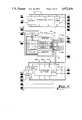
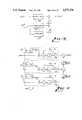
- FIG. 1is a block schematic diagram illustrating a modem incorporating a sigma delta modulator based analog front end constructed in accordance with the preferred embodiment of the present invention.
- FIG. 2is a spectral diagram illustrating the required technical performance requirements for the receiver signal-to-noise ratio for a high speed low distortion modem such as a V.32 modem.
- FIG. 3is a conceptual diagram illustrating the analog-to-digital conversion stage employed in the preferred embodiment shown in FIG. 1.
- FIG. 4is a block schematic diagram illustrating the analog-to-digital conversion stage employed the preferred embodiment shown in FIG. 1.
- FIG. 5is a detailed schematic diagram of the preferred embodiment of the four phase clocked sigma delta modulator analog-to-digital converter constructed in accordance with the preferred embodiment of the present invention, as employed in the modem of FIG. 1.
- FIG. 6,consisting of FIGS. 6A and 6B, is a schematic diagram and timing diagram showing error and waveform distortion caused by charge injection in a prior art two phase switched capacitor integrator circuit.
- FIG. 7is a schematic diagram illustrating a prior art four phase switched capacitor integrator circuit.
- FIG. 8is a timing diagram illustrating the four phase clocking scheme employed in the preferred embodiment of a switched capacitor integrator circuit.
- FIG. 9is a "floorplan" layout diagram of an analog integrated circuit chip of the preferred sigma delta modulator circuit illustrated in FIGS. 3 and 4.
- FIG. 10is a more detailed floorplan layout diagram of the analog integrated circuit chip shown in FIG. 9, showing the symmetrical wiring layout.
- FIG. 11is a generalized block diagram of an FIR digital filter of length N.
- FIG. 12is a generalized block diagram of the FIR filter of FIG. 11 divided into functional blocks to effectuate decimation.
- FIG. 13illustrates the application of Tellegan's Theorem to the block diagram of FIG. 12.
- FIG. 14illustrates a ROM-based equivalent block diagram for the FIR filter of FIG. 13.
- FIG. 16illustrates the application of Tellegan's Theorem to the block diagram of FIG. 15.
- FIG. 17illustrates an expanded form of the block diagram of FIG. 16 in a form suitable for VLSI implementation.
- FIG. 19is a schematic block diagram of the sigma delta modulator digital to analog converter employed the preferred embodiment shown in FIG. 1.
- FIG. 20is a block diagram of a digital sigma delta modulator employed in the preferred sigma delta modulator digital to analog converter shown in FIG. 19.
- FIG. 21is a detailed schematic diagram of the return-to-zero one bit differential digital to analog converter employed in the preferred sigma delta modulator digital to analog converter shown in FIG. 19.
- FIG. 1there is illustrated an analog front end circuit 10 in a modem 12, all constructed in accordance with the preferred embodiment of the present invention.
- the modem 12in addition to the analog front end circuitry 10, includes several other components, many of which are conventional and will be known to those skilled in the art.
- the preferred embodimentis included in a modem which typically includes a microprocessor, which is included within the other modem circuits.
- An external data terminal 8which may be a digital computing machine or some other digital device, communicates with and is connected to the modem 12 by an RS-232C interface 11.
- the modem 12is also connected to a subscriber telephone line 15 so that data may be exchanged with some remote device.
- the modem 12converts data from the RS-232C format to a format suitable for transmission over a telephone line 15, and vice versa.
- the analog front end circuits 10 in FIG. 1are connected to other modem circuits 16.
- the other modem circuits 16comprise, for example, signal input and output conditioning and isolation circuits, voltage regulators and filters, phase locked loops, status indicators, frequency synthesizers, memory, and a microprocessor/controller, all of which will be known to those skilled in the art. Exemplary details of how the various functions of a modem are controlled by a microprocessor are found in U.S. Pat. Nos. 4,431,867 and 4,504,802, which are assigned to the assignee of the present invention.
- the other modem circuits 16provide data for outgoing transmission via a DATA IN bus 13, through modulator 17, and to the front end circuit 10.
- the other modem circuits 16receive demodulated data from an incoming transmission on DATA OUT bus 14 from digital signal processing circuits 24.
- the modem front end 10prepares data for transmission over the telephone line 15.
- the modulator circuit 17receives the data for transmission over bus 13 and provides an analog modulated signal to the front end circuitry 10.
- the modulator 17may be constructed as described in U.S. Pat. No. 4,504,802 to Heatherington, which is also owned by the same assignee as the present invention.
- the output of modulator 17is therefore a four-phase differential phase shift keyed digital signal which is then provided to the modem front end 10, and in particular to a digital-to-analog (D/A) converter 18 contained therein.
- the output of the D/A converter 18is then provided to a conventional telephone company hybrid circuit 20, which is connected to the telephone line 15.
- Incoming signals from the telephone lineare provided through the hybrid circuit 20 to a sigma delta analog-to-digital (A/D) converter 19, also within the front end circuitry 10.
- the output of the sigma delta A/D converter 19is provided to a summing circuit 21, which is digital, which combines the digital output with signals from a conventional echo cancelling circuit 22.
- echo in data telecommunicationsis composed of several elements.
- the "near end" echocomprises leakage from the modem hybrid circuits 20, on the order of 6-8 dB below the transmitted signal level.
- Another component of near end echois that from the central office hybrids. These hybrids are never truly matched to the line, and some of the transmitted energy will return from these hybrids as echo.
- the near end and far end echoesare subtracted from the total composite received signal, supposedly leaving only the signal transmitted from the far end modem.
- the preferred echo canceller 22 in the modem 12is assumed to be linear, and comprises an adaptive linear transversal FIR digital filter which provides on the order of 75 dB of echo cancellation. If one assumes that transmissions occur at 0 dBm, what is received from the other modem is on the order of -45 dBm. In order to effectively carry out V.32 or the like demodulation correctly, there needs to be 22-23 dB signal-to-noise ratio, or more conservatively 30 dB. Accordingly, a noise floor of -75 dB as seen by the receiver is required. This means that the transmitted data must be attenuated by 75 dB with the echo canceller 22, because the transmitted data basically shows up as noise to the receiver.
- the digital echo-cancelled signalafter the echo canceller 22, is provided then to a digital signal processing circuit 24 (DSP), which performs additional modem functions such as demodulation, timing signal recovery, decision making, and adaptive equalization, and then provides the DATA OUT digital signals on bus 14.
- DSPdigital signal processing circuit 24
- FIG. 2is an example of typical requirements for receiver signal-to-noise ratios which must be present in order to minimally meet the V.32 standards. If the maximum signal level at the transmitter (TX) is at 0 dBm for reference, then the minimum signal at the receiver (RCV) is specified at no lower than -43 dBm from the transmitter. With a receiver signal-to-noise ratio of 21 dBm, the total noise floor must be set at -64 dBm.
- the performance level of the receivermust be -78 dBm or better.
- signal-to-noise ratios on the order of -105 dBmare possible.
- oversamplingis a known method of reducing quantization noise, it usually increases bandwidth.
- the sample ratebe defined as 2 L f n , where f n is the Nyquist frequency, and L is number of octaves of oversampling.
- f n9600
- a voice-grade telephone lineonly exhibits a bandwidth of about 3600 Hz
- the highest frequency of interestis about 3500-3600 Hz for a modem.
- About 4800 Hzwould be required for frequency division multiplexing on a dedicated line, but there is not enough bandwidth for conventional voice grade telephone lines.
- For frequency division multiplexingabout 2400 Hz of bandwidth is required for transmitted data, with a guard band of at least 100 Hz, and 2400 Hz for received data, for a total of 4900 Hz, but this exceeds the available bandwidth.
- the bandwidth requirementis 7000 Hz minimum, which is two times the bandwidth of 3500 Hz, so either 7200 or 9600 is selected to be an even multiple of two. Since the baud rate is 2400, and since it is desirable to have an even multiple of the baud rate for digital signal processing, 9600 emerges as the bit transfer rate.
- Quantization noiseis a fixed feature for a fixed number of converter bits. For a conventional twelve bit A/D converter, quantization noise is on the order of 72 dB. By oversampling, there is about 3 dB per octave enhancement; every time the sampling rate is doubled, the noise in the band is halved. Quantization noise appears as white noise, spread out evenly across the band.
- the sigma delta A/D converter 19comprises a sigma delta modulator circuit 25 which receives the input analog signal from the hybrid circuit 20 on line 23.
- the sigma delta modulator 25 outputis a digital bit stream at a sample rate of 1.2288 MHz.
- This bit streamis then provided to a low pass filter 26 for purposes of substantially eliminating quantization noise above a predetermined cut-off frequency; the quantization noise is effectively shifted above the cut-off frequency of the low pass filter 26 by the operation of the sigma delta modulator 25.
- the low pass filter 26provides a parallel 16 bit signal to a decimator circuit 30, which decimates the digital signal to achieve a 9600 per second sample rate.
- the output of the decimator 30, and thus of the sigma delta A/D converter 19,is 9600 samples per second, each sample comprising 16 parallel bits of information, and wherein the quantization noise has been substantially eliminated by low pass filtering.
- the A/D converter 19in the preferred embodiment converts samples at a rate of 800 nanoseconds in order to satisy the 9600 bit per second data rate, which corresponds to 1.2288 megasamples/sec. This is a very fast sampling rate, and currently available digital signal processing circuits are hard pressed to operate at these rates. Conventional digital signal processing is usually optimal at a sampling rate of about 10 kHz, which is well below the required rate of 1.2288 MHz. Accordingly, the digital decimator 30 gets rid of oversamples.
- the decimator 30brings down effective sampling rate by a factor of 128. This is done in two stages in the preferred embodiment, as shown in FIG. 4. There is a first decimation filter stage 30a which reduces by a factor of 32, and the second is a second decimation filter stage 30b which reduces by a factor of 4.
- the first stage decimation filter 30ais a novel filter constructed as described hereinbelow, as an improved FIR decimating filter.
- the second stage 30bis more conventionally constructed, and in the preferred embodiment is constructed in accordance with the paper by Candy et al., "A Voiceband Codec with Digital Filtering," IEEE Trans. Commun., vol. COM-29, pp. 815-830, June 1981, which is incorporated by reference herein and made a part hereof.
- the low pass filter 26is a digital filter of the type ##EQU1## which will be known to those skilled in the art. Further details pertaining to the decimator 30 are provided below.
- An analog second order anti-aliasing filter 31receives the analog input signal on line 23 prior to the sigma delta modulator 25. After filtration, the signal is then provided to the switched capacitor sigma delta modulator 25. The circuit operates with a 1.228 MHz sample clock so that there are about eight octaves of oversampling, assuming that the bandwidth of the input signal does not exceed about 4 kHz. The low pass filter 26 then receives a serial bit stream at 1.228 MHz, and provides a sixteen parallel bit output word to the decimator 30.
- the decimator 30 in FIG. 4comprises a first digital decimating filter 30a which has an output word rate of 38.4 kHz, followed by a second digital decimating filter 30b which has an output word rate of 9.6 kHz, yielding sixteen bit words.
- the first digital decimating filter 30ais a FIR and the second digital decimating filter 30b is an IIR.
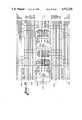
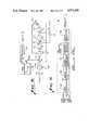
- FIG. 5is a detailed schematic diagram of the sigma delta modulator 25 employed in the A/D converter 19 constructed in accordance with the preferred embodiment of the present invention.
- conventional sigma delta modulatorsdo not provide sufficient performance capability for use in the present invention. Accordingly, several features in particular are provided in the sigma delta modulator 25 of the present invention, which improve performance to an extent very close to the theoretically achievable performance.
- a pair of differential integrators 40a, 40bare provided in series at the input end, to integrate the differential input signal provided on line 23.
- the use of differential integrators and differential signalsensures that any common mode errors will not affect the performance.
- each of the integrators 40a, 40bis clocked with the novel four-phase clocking scheme, to be described in detail below.
- double integrationis effectuated with the integrators 40a, 40b, which avoids overloading and allows the achievement of signal-to-noise ratios on the order of -105 dB.
- the output of the second integrator circuit 40bis provided on line 42 and comprises a 1.288 MHz serial digital bit stream, each pulse having an identical width, which is suitable for provision to a digital low pass filter 26.
- the analog input signal on line 23is provided to the first integrator 40a and comprises the signals A in + and A in - . These signals are first provided through a first switching MOSFET transistors M2+, M2-, and thence to sampling capacitors CS1+, CS1-. Both MOSFETs M2+, M2- are clocked at time ⁇ 1b. The timing signals are discussed in more detail in connection with FIG. 8.
- a pair of second MOSFET transistors M3+, M3-are connected to a first plate of the sampling capacitors CS1+, CS1-, respectively, and at time ⁇ 2b connect ground to the first plate of the capacitor.
- the opposite or second plates of the sampling capacitors CS1+, CS1-are connected through MOSFETs M4+, M4-, respectively, to the inverting and noninverting inputs, respectively, of a differential operational amplifier 45a. Both MOSFETs M4+, M4- are switched at time ⁇ 2a. Switching MOSFET transistors M1+, M1- connect ground to the second plates of the sampling capacitors CS1+, CS1-, respectively, at time ⁇ 1a.
- the integration functionis performed by integrating capacitors CI1+, CI1-, which are connected as follows: the noninverting output of the op amp 45a is fed back to the inverting input through integrating capacitor CI1+ to the inverting input, while in like manner the inverting output is fed back through integrating capacitor CI1- to the noninverting input.
- the differential outputs of the op amp 45a, and thus of the integrator circuit 40a,are cascaded to a second integrator stage 40b which is constructed exactly as is circuit 40a.
- a second integrator stage 40bwhich is constructed exactly as is circuit 40a.
- the second integrator stage 40bis clocked with the novel four phase clocking method as the first integrator stage 40a, described in connection with FIG. 8.
- the output of the integrator circuit 40bis then provided in differential form to a comparator circuit 43, which provides an output when there is a non-zero voltage between the two input lines 48.
- the output of comparator 47is provided to the D input of a delay-type flip flop 47, which is clocked with the clock signal ⁇ 1a.
- the Q output of the flip flop 47is the output signal DOUT on line 42, which is a digital 1.2 M bps bit stream.
- feedback capacitors CF1+, CF1, CF2+, CF2-form parts of the inner and second loops of feedback for sigma delta modulation, and correspond to the inner and second loops of the quantizer shown in FIG. 3 of the paper by James C. Candy, "A Use of Double Integration in Sigma Delta Modulation," IEEE Trans. Comm., Vol. COM-33, No. 3, March 1985, pp. 249-258, at p. 251, the disclosure of which is incorporated herein by reference and made a part hereof.
- the outputs of the flip-flop 47are used essentially as voltage references (+VR, -VR) for the op amps 45a, 45b, and switched at appropriate points in the timing cycle.
- the feedback capacitorsperform the function of D/A conversion, since the latch output is a digital serial bit stream signal. All the feedback capacitors CF1+, CF1, CF2+, CF2- are connected to MOSFET switches which connect the capacitors between the latch 47 output and a summing node at the inputs of the op amps 45a, 45b. The switching occurs at time ⁇ 1b to make the feedback connection and at time ⁇ 2b to connect to ground. It will thus be appreciated that the structure of the feedback capacitors using the outputs of the latch as reference voltages merely performs a D/A conversion function so as to provide the appropriate feedback signal levels into the integrators.
- FIG. 6illustrates the error and waveform distortion caused by charge injection in a conventional two-phase switched capacitor integrator.
- the circuit of FIG. 6Ais a conventional single ended (i.e., non-differential) switched capacitor integrator circuit, which is clocked with the two-phase clock as shown in FIG. 6B.
- the two-phase clockconsists of two non-overlapping clock signals, ⁇ 1 and ⁇ 2.
- the input signal V inis shown as a rising input voltage.
- V CSis the sampling capacitor voltage as the sampling capacitor CS charges up during the signal sampling process.
- MOSFET type transistorsWhen a MOSFET is turned on, a quantity of charge is stored in its channel. When the transistor is turned off by the falling edge of a clock signal at its gate, this charge is dissipated or injected into the neighboring circuit nodes. This charges causes an error in the sampled and integrated voltage represented by the charge stored on the sampling capacitor.
- V Ggate voltage (e.g., 5 volt clock signal)
- V TMOSFET threshold voltage
- V G 'V G -V T ,
- V channelchannel voltage
- V ininput voltage
- C oxidegate oxide capacitance of M.
- the charge errorcomprises two separate components, a first being dependent only of the gate threshold voltage (for the clock) and a second being dependent on the sampled signal level.
- the former componentneed not be considered a source of error because because it gives rise to an offset voltage that is cancelled by the common mode rejection behavior of fully differential circuits.
- all circuits used hereinare differential so as to eliminate this possible source of error.
- M3turns off at the falling edge of ⁇ 2, but the charge ⁇ Q 2 injected into CS due to that transition is not signaldependent as the op amp input node is always being switched between ground and virtual ground, and therefore causes no distortion.
- M2will turn off before M1, even though both are clocked by ⁇ 1.
- the charge injected by M2 turning OFF ( ⁇ Q 1 )will distribute partially into CS and partially back into the driving source at the integrator input (typically an op amp or buffer).
- the integrator inputtypically an op amp or buffer.
- the charge sampled on CS during ⁇ 1has been completely transferred to CI.
- the ⁇ 2 clock waveformnow has a high-to-low transition turning OFF transistors M3 and M4. This again causes charge injection into CI.
- a second error ⁇ Q 2is ejected into CS. This causes a signal-dependent distortion consisting of the two charge components ⁇ Q 1 and ⁇ Q 2 , as illustrated in FIG. 6B. Accordingly, there is a need for a switched capacitor integrator circuit which does not cause error and waverform distortion caused by charge injection.
- phase clocking schemesare known for use in switched capacitor filters, for example the paper by Lee & Meyer, "Low Distortion Switched Capacitor Filter Design Techniques", IEEE JOURNAL OF SOLID STATE CIRCUITS, Vol. SC-20, No. 6, Dec. 1985, proposes a four phase clocking scheme for reducing distortion caused by clock feedthrough and charge injection.
- this particular four phase clocking schemefails to recognize that the charge injection problem is primarily due to the sequence of connecting and disconnecting the input signal to the sampling capacitors, and therefore does not provide an adequate solution to the problem of charge injection.
- the clocking scheme for the integrators 40a, 40bdiffers in a significant aspect from known prior art four-phase switched capacitor integrator clocking schemes, such as the one shown in the Lee & Meyer article.
- the novel clocking scheme employed in the present inventionsubstantially reduces the distortion which may be caused by charge injection in the MOSFETs. It has been discovered that prior art techniques for connecting the sampling capacitors to the integration circuit allow an incremental charge to be accumulated in the physical structure of the MOSFETs, which accumulates and is ultimately injected into the sampling capacitor and provides the distortion component. Discovery and analysis of this problem resulted in the improved four-phase clocking system employed in the preferred embodiment.
- the phases of the clockare such that ⁇ 1b follows ⁇ 1a by about 10 nanoseconds, and that ⁇ 1a and ⁇ 1b therefore overlap. Thereafter ⁇ 2a occurs, followed about 10 nanoseconds later by ⁇ 2b. ⁇ 2a and ⁇ 2b slightly overlap, but neither of these pulses overlap either of ⁇ 1a or ⁇ 1b.
- ⁇ 1a and ⁇ 1b ONM2 and M1 ON, the input is sampled on CS.
- ⁇ 1a OFF and ⁇ 1b ONM1 turns OFF, its signali-ndependent charge is injected into CS and CI, causing voltage offset but no distortion.
- ⁇ 2a and ⁇ 2b ONM4 and M3 ON, the charge on CS is transferred to CI (i.e., integrated).
- ⁇ 2a OFF and ⁇ 2b ONM4 turns OFF, its signal-independent charge is injected into CS and CI, causing voltage offset but no distortion.
- ⁇ 2a and ⁇ 2b OFFM3 turns OFF. Since the other side (the CS side) of the MOSFET switch is not connected to the op amp 45 and integrating capacitor CI, the charge returns to ground.
- the actual implementation in the preferred circuitis fully differential, thus cancelling effects of voltage offset, capacitance and op amp gain nonlinearities, and op amp slew rate nonlinearity.
- the fully differential implementationresults in a first order noise cancellation that also improves the overall signal-to-noise dynamic range of the A/D converter.
- the clock signals ⁇ 2a and ⁇ 2bare reversed when compared to the prior art clocking arrangement.
- the MOSFETs M4are switched by the clock signal ⁇ 2a in the preferred embodiment, but clocked by ⁇ 2b in the prior art.
- the MOSFETs M3are switched by the signal ⁇ 2b in the preferred embodiment, but by ⁇ 2a in the prior art.
- the effect of this change in switching of the MOSFETs M3 and M4is that in the preferred embodiment, M4 switches off before M3, thereby preventing signal-dependent charge injection through the sampling capacitors CS into the integrating capacitors CI.
- the present inventionfurther comprises integrated circuit layout features which minimize clock feedthrough and other distortion mechanisms which are common in combination analog and digital integrated circuits.
- these featuresallow construction of a sigma delta modulator based A/D converter with very high performance of 105 dB of signal-to-noise ratio.
- Those skilled in the artwill understand that it has always been a difficult design challenge to provide both analog and digital functions on a single semiconductor chip.
- the present inventionis constructed so as to provide 105 dB or better signal-to-noise ratio, it has been discovered that the arrangement and layout of the various portions of the sigma delta modulator with respect to other portions of the analog circuitry are important factors in maintaining the desired signal-to-noise ratio.
- the basic layout of the analog front end 12is illustrated, exclusive of certain digital portions.
- the sigma delta A/D converter 19bis positioned in the center of the integrated circuit chip 60. Signals received from the hybrid circuit 20 (not shown in FIG. 9) are received on line 23 and provided to a receiver programmable gain amplifier 61, and then to the antialiasing filter 31. From the antialiasing filter 31, differential signals on lines 63 are provided to the sigma delta A/D converter 19b. Digital signals are confined to digital bus 65, and the layout specifically contemplates a minimum number of crossings of the digital lines with analog signals. In particular, it will be noted that the digital signals only cross at six different places, which are denoted as 66a, 66b, . . . 66f.
- the audio path circuit 74receives the output of the antialiasing filter 31 and provides an audio signal path to a monitor on the MON output. Many of these functions are not required in implementing the present invention, and are provided here so that a complete disclosure of the environment in which the present invention operates may be more fully understood.
- FIG. 10more particularly illustrates the particular layout features of the sigma delta modulator 25 and particularly illustrates the arrangement of the integrating capacitors CI, sampling capacitors CS, and op amps 45 so as to isolate the analog circuitry from digital control signals which can distort the operation of the A/D converter 19b.
- the integrator circuits 40a, 40bare positioned between rows of longitudinally extending power and ground buses 80a, 80b and digital signal buses 81a, 81b so as to provide maximum spatial isolation of the analog circuits from digital circuits.
- Analog switcheswhich comprise the MOSFETs M1+, M1-, M2+, M2-, M3+, M3-, and M4+, M4- are contained within the switch regions 82a, 82b, which are positioned between the power and ground buses 80a, 80b and the digital signal buses and clocks 81a, 81b.
- Each of the power and ground buses 80a, 80binclude signals, working from the inside out, VBIAS, AVSS, AVDD, AGND, -VR, +VR, and VINT.
- VBIASis a biasing signal for the op amps 45a, 45b.
- AVSS and AVDDare power supply lines, while AGND is a ground line for the analog circuitry.
- -VR and +VRare reference voltages, while V in + and V in - are the differential analog input voltages.
- the digital signal buses 81a, 81bcomprise a two-phase clocking signal ⁇ 1, ⁇ 2, each of which has a period of 1/1.2288 MHz (about 815 nanoseconds) and is delayed by 4 nanoseconds as described in connection with FIG. 8 in order to obtain the four 1.2288 MHz four-phase clock signals ⁇ 1a, ⁇ 1b, ⁇ 2a, ⁇ 2b.
- the digital output signalis denominated DOUT.
- sampling capacitors CS1+, CS1-are positioned on the right-hand side of the chip (when viewing the chip as oriented as shown in FIG. 10), followed moving right to left by the integrating capacitors CI1+, CI1-, followed again moving to the left by the op amp 45a. It will be understood that all of these capacitor areas are formed in a common region on the chip for ease of fabrication.
- the sampling capacitors CS2+, CS2-are positioned adjacent to the op amp 45a, moving right to left, followed next by the integrating capacitors CI2+, CI2-, followed by the op amp 45b.
- the output of the op amp 45bare the differential signals OUT+, OUT-, which are provided to the comparator 47 which is positioned further to the left (FIG. 110).
- the low pass filter 26 and decimating filter 30a in the preferred embodimentis a novel implementation of an FIR filter of length N, having N coefficients ⁇ h o , h 1 , . . . h N ⁇ , including a decimation stage.
- a generalized block diagram for such a filter 120is shown in FIG. 11. The inputs of this filter are digital samples separated in time by T.
- decimation of an input data streamis required in the present invention, an output is only required after a multiple of k input sample periods, i.e., one output occurs for every k input samples.
- input signal x(nT)is sampled every T seconds, delayed by delay units 121 by z -1 , and multiplied by coefficients h i by multipliers 122.
- the outputs of the multipliers 122are then summed by adder 123, and the output of the adder is sampled at the rate of 1/kT by a switch 124 for decimation to obtain the filtered output signal y(knT).
- the generalized filter of FIG. 11can be described in a way that takes advantage of the fact that the output is only calculated once for every k input samples, shown as filter 120' in FIG. 12.
- the input samplesare shifted k times through the shift register comprising the delay units 121 between calculations of the output samples y(knT).
- An additional adder stage 131is employed to add the outputs of the subfilters 130.
- Tellegan's theoremindicates that an equivalent filter can be built by reversing the direction of flow through the filter.
- An exemplary subfilter 130' of order k redrawn using this theoremis shown in FIG. 13, and can be represented by the equation: ##EQU3## It will be appreciated that after application of Tellegan's theorem, the input signal x(nT) is multiplied by the coefficients h i in parallel, delayed by the delay units 121, and then added with the adders 123 to a delayed version of the previous stages.
- Switch S3selects the filter coefficients in the required order, and comprises a counter (not shown) for stepping through the addresses of the ROM 136.
- the delay z -kbecomes a unit delay z -1 if it is moved to the other side of the decimation switch S 1 .
- the subfilterprocesses one input sample at a time at the input rate 1/T and produces one output sample at the decimated rate 1/kT.
- the subfilter accumulatoronly operates once for each input sample. When the hardware for L subfilters is multiplexed, the accumulator operates L times for each input sample.
- the filter 150employs a one-bit latch 151a and sixteen-bit latches 151b, 151c, 151d, 151e as transparent means for implementing the z -1 delay registers.
- the ROM 152stores the coefficients h i , and a seven bit counter 153 steps through the ROM addresses with a clock CLK having a rate of L/T.
- Latch 151aholds the input sample x(nT) for L second clock periods.
- the multiplier 154in this case comprises a set of exclusive-OR gates since x(nT) only takes on the values ⁇ 0,1 ⁇ .
- the ROM 152preferably stores the subfilter coefficients, each of n bits, in an interleaved fashion. Alternatively, the coefficients can be stored in their original sequence as in the direct form FIR filter of FIG. 11. In the latter case, it will be understood that the coefficients can be interleaved by changing the address lines of the ROM.
- Switch S 2connects the output of register/latch R 1 to register/latch R 2 for all clock periods except when the output of R 1 is sampled on switch S 1 .
- the clock period for switch S 1is 1/kT, which is the decimation frequency. Accordingly, the S 1 frequency may be considered a third clock when compared to the first or data input clock at frequency 1/T. Every 1/kT or third clock period, S 2 connects all zeroes to clear the contents of R 2 .
- the first type of clockconnected to the switch S 4 , occurs consecutively for k-1 times, and is the input sample rate.
- the second type of clockconnected to the counter 153 and switch S 3 , occurs for L(k-1) times.
- the third type of clock cycleconnected to switches S 1 and S 2 , occurs on the kth occurrence of the first type of clock cycle.
- the third clock cycle typeoccurs with S 3 open, S 1 closed, and S 2 switched to reset register/latch R 2 .
- S 4is closed on every Lth second clock cycle and is coincident with the k-1th clock cycle. On each second clock cycle, the following operations occur simultaneously:
- R 1will contain the accumulation for the first subfilter
- R 2will contain the accumulation for the second subfilter
- so onAfter L cycles of the second clock, an additional iteration has occurred for each subfilter. This occurs for L.k clock cycles when the output of each subfilter is complete. At this point, the output of the first subfilter is sampled. During this cycle, no data is shifted between the remaining registers and the register/latch R 2 is cleared. This has the effect of implementing the z -k delay element of FIG. 17. The output from the last subfilter is moved to the accumulator of the next to last subfilter and so forth.
- the conventional filter form of FIG. 11would require 96 shift registers, 96 adders, and 96 multipliers.
- the preferred embodiment of FIG. 18uses one 16 bit adder 155, four 15 bit register/latches, one multiplier (primarily exclusive-OR gates), and a ROM to store the coefficients. It will thus be appreciated that the general decimating filter 150 of FIG. 18 may be efficiently implemented with VLSI logic, and substantial savings of chip area are possible.
- the preferred D/A converter 18takes a 16 bit digital code at the rate of 9600 words per second from the modulator 17 (FIG. 1) and converts it into an analog signal for transmission by the hybrid circuit 20 over the telephone line 15.
- the D/A converter 18comprises a first interpolator 161 which generates oversamples at the rate of 4:1 to obtain 38.4 kilosamples per second, by an interpolation process.
- a second 32:1 interpolator 162takes the output of the first interpolator 161 and generates a 1.2288 megasamples per second, still of sixteen bits per sample.
- interpolation by both interpolators 161, 162is carried out in the manner described with respect to FIG. 10 of the paper by Candy et al., "A Voiceband Codec with Digital Filtering," IEEE Trans. Commun., vol. COM-29, pp. 815-830, June 1981, referenced hereinabove.
- the output of the interpolator 162is provided to a digital sigma delta modulator 163, which is described in greater detail in connection with FIG. 20.
- the output of the sigma delta modulator 163is provided to a return to zero digital to analog converter 165, and thence to an analog antialiasing filter 168, essentially a low pass filter.
- the return to zero digital to analog converter 165 and the analog antialiasing filter 168are described in greater detail in connection with FIG. 21.
- the sigma delta modulator 163is constructed substantially as described in connection with FIG. 3 of the paper by Candy, "A Use of Double Integration in Sigma Delta Modulation," referenced above.
- a digital implementation of the sigma delta modulator 163is shown in FIG. 20.
- the 1.2288 megasample per second input signal from the interpolator 162is first provided to a sixteen bit adder 170 which corresponds to the outer feedback loop or first subtraction stage in the referenced Candy paper.
- the other operand for adder 170is the two's complemented output of the circuit, provided on lines 171.
- a digital two's complement circuit 173performs this function in the known manner, so that the adder 170 carries out a subtraction function for the negative feedback.
- the digital signalpasses to a second adder 172, which corresponds to the first adder after the G 2 gain stage in the referenced Candy paper.
- the other operand to the adder 172is the output of a first accumulator 174, which corresponds to the first delay in the referenced Candy paper.
- the accumulator 174 and adder 172carry out the first level of integration in the double integration process.
- the signalpasses to a third adder 176, which corresponds to the inner loop or second subtraction stage in the referenced Candy paper. Accordingly, the other operand to the adder 176 is the two's complemented output on lines 171. From the adder 176 there is a fourth adder 178, which corresponds to the adder after the G 1 gain stage in the referenced Candy paper. The other operand to the adder 178 is the output of a second accumulator 179, which corresponds to the second delay in the referenced Candy paper. The accumulator 179 and adder 178 carry out the second level of integration in the double integration process.
- the referenced Candy paperemploys a quantizer as the final stage in the double integrator sigma delta modulator.
- all that is requiredis to select the most significant bit (MSB) of the sixteen bit signal from the output of adder 178 in order to obtain a one bit quantizer.
- MSBmost significant bit
- the output of the digital sigma delta modulator 163is the MSB, denominated 1 BIT MODULATED CODE. This output is provided to a return-to-zero one bit D/A converter 165.
- the return-to-zero circuit 165reduces distortion caused by unequal rise and fall times of the incoming signal, and the antialiasing or low pass filter 168 averages the sequences of return-to-zero corrected pulses so as to obtain a low pass filtered analog signal, and provides signal isolation and amplification.
- the return-to-zero (RTZ) circuit 165eliminates distortion induced by asymmetrical rise and fall times of the pulse output from the digital sigma delta modulator 163.
- the problem of non-equal rise and fall timeshas been addressed in the prior art by trying to use special CMOS drivers with matched P and N transistors and by using circuit techniques to achieve faster rise and fall times. It is believed that the mechanism that causes the distortion is the fact that the energy of adjacent pulses do not add linearly. The reason for nonlinear addition is believed to be due to the fact that rise and fall times of the pulses are not equal.
- the problemis solved by a method of making adjacent pulses add linearly without requiring equal rise and fall times.
- the methodentails making each pulse short enough so that it will not overlap in time with adjacent pulses. It is required that a given pulse falls to zero (including the fall time) before the next pulse starts.
- the RTZ circuit 165comprises a pair of series-connected D-type flip flops 181a, 181b which are clocked by the signal CONVERTER CLOCK, which occurs at the 1.2288 MHz system clock rate.
- the reset (R) input of the flip flop 181bis connected through an inverter 182 to the CONVERTER CLOCK so that the flip flop is clear on the trailing edge of the clocking signal.
- the input signal 1 BIT MODULATED CODEis provided to the D input of flip flop 181a, and the Q output of this flip flop is connected to the D input of flip flop 181b.
- the Q output of the flip flop 181bis provided to the low pass filter 168.
- the output of the RTZ circuit 165therefore comprises a 1.2288 MHz serial digital bit stream, each pulse having an identical width, which is suitable for provision to the digital low pass filter 168.
- the return-to-zero functionis provided in the circuit 165 by inverting the CONVERTER CLOCK through inverter 182. It will thus be appreciated that a "zero" provided as the input will propagate through both flip-flops 181a, 181b to the output as a zero. On the other hand, a "one" will appear after one propagation delay through flip-flop 181b, as clocked in by the CONVERTER CLOCK, and will then be "returned to zero" when the positive edge of the CONVERTER CLOCK has propagated through the inverter 182 and reset the flip-flop 181b.
- each pulse from the digital sigma delta modulator 163 which represents a "one”should be short enough so that it will not under any circumstances overlap in time with an adjacent "one".
- Each "one”will be separated by at least the time of the CONVERTER CLOCK.
- the return-to-zero (RTZ) circuit 165therefore makes sure that for every bit of the incoming signal 1 BIT MODULATED CODE the output signal returns to zero, whether a "one" or “zero”, by splitting up into two phases. In the first phase the value of the bit is represented, whether "one” or “zero”, and in the second phase the signal returns to zero. Thus, the net energy represented by a "one” is always the same, and the net energy represented by a zero is always the same.
- the return-to-zero circuit 165may find usefulness in circuits other than sigma delta modulators, for example, pulsewidth modulation coders, interpolating coders, delta modulation coders, and noise shaping coders.
- pulsewidth modulation codersfor example, pulsewidth modulation coders, interpolating coders, delta modulation coders, and noise shaping coders.
- such a return-to-zero approachcan provide additional improvement in signal-to-distortion ratio on the order of 60 dB or better in many applications.
- the analog antialiasing filter 168is a conventional low pass active filter having essentially unity gain constructed around an operational amplifier 185, with resistors R all having a value of 10k ohms, and capacitor C having a value of 1000 pF.
- the output of the filter 168is the signal ANALOG OUT, which is provided to the telco hybrid circuit 20 (FIG. 1).
Landscapes
- Engineering & Computer Science (AREA)
- Theoretical Computer Science (AREA)
- Compression, Expansion, Code Conversion, And Decoders (AREA)
Abstract
Description
ΔQ=C.sub.oxide (V.sub.G '-V.sub.channel)=
R.sub.1 →X(n)h.sub.i +R.sub.4, R.sub.4 →R.sub.3, R.sub.3 →R.sub.2, R.sub.2 →R.sub.1
R.sub.1 →R.sub.1, R.sub.2 →O, R.sub.3 →R.sub.3, R.sub.4 →R.sub.4, Y(knT)=R.sub.1
Claims (39)
Priority Applications (2)
| Application Number | Priority Date | Filing Date | Title |
|---|---|---|---|
| US07/257,733US4972436A (en) | 1988-10-14 | 1988-10-14 | High performance sigma delta based analog modem front end |
| CA000586437ACA1314629C (en) | 1988-10-14 | 1988-12-20 | High performance sigma delta based analog modem front end |
Applications Claiming Priority (1)
| Application Number | Priority Date | Filing Date | Title |
|---|---|---|---|
| US07/257,733US4972436A (en) | 1988-10-14 | 1988-10-14 | High performance sigma delta based analog modem front end |
Publications (1)
| Publication Number | Publication Date |
|---|---|
| US4972436Atrue US4972436A (en) | 1990-11-20 |
Family
ID=22977526
Family Applications (1)
| Application Number | Title | Priority Date | Filing Date |
|---|---|---|---|
| US07/257,733Expired - LifetimeUS4972436A (en) | 1988-10-14 | 1988-10-14 | High performance sigma delta based analog modem front end |
Country Status (2)
| Country | Link |
|---|---|
| US (1) | US4972436A (en) |
| CA (1) | CA1314629C (en) |
Cited By (118)
| Publication number | Priority date | Publication date | Assignee | Title |
|---|---|---|---|---|
| US5030954A (en)* | 1990-09-17 | 1991-07-09 | General Electric Company | Double rate oversampled interpolative modulators for analog-to-digital conversion |
| US5057839A (en)* | 1989-05-08 | 1991-10-15 | Siemens Aktiengesellschaft | Integratable switched-capacitor sigma-delta modulator |
| US5170387A (en)* | 1989-05-08 | 1992-12-08 | U.S. Philips Corporation | Apparatus for reading an information pattern from a record carrier and signal-processing circuit for use in such apparatus |
| GB2256551A (en)* | 1991-06-06 | 1992-12-09 | Crystal Semiconductor Corp | Switched-capacitor integrator with chopper stabilization performed at the sampling rate |
| US5181033A (en)* | 1992-03-02 | 1993-01-19 | General Electric Company | Digital filter for filtering and decimating delta sigma modulator output signals |
| US5222084A (en)* | 1990-06-25 | 1993-06-22 | Nec Corporation | Echo canceler having adaptive digital filter unit associated with delta-sigma modulation circuit |
| US5274375A (en)* | 1992-04-17 | 1993-12-28 | Crystal Semiconductor Corporation | Delta-sigma modulator for an analog-to-digital converter with low thermal noise performance |
| US5317529A (en)* | 1991-04-23 | 1994-05-31 | Mitsubishi Denki Kabushiki Kaisha | Digital filter using intermediate holding registers and common accumulators and multipliers |
| US5321320A (en)* | 1992-08-03 | 1994-06-14 | Unisys Corporation | ECL driver with adjustable rise and fall times, and method therefor |
| US5349352A (en)* | 1992-12-21 | 1994-09-20 | Harris Corporation | Analog-to-digital converter having high AC line noise rejection and insensitive to AC line frequency variations |
| US5386438A (en)* | 1993-09-14 | 1995-01-31 | Intel Corporation | Analog front end integrated circuit for communication applications |
| US5394392A (en)* | 1992-12-14 | 1995-02-28 | At&T Corp. | Method for transferring information using modems |
| US5450083A (en)* | 1994-03-09 | 1995-09-12 | Analog Devices, Inc. | Two-stage decimation filter |
| US5528239A (en)* | 1992-04-17 | 1996-06-18 | Crystal Semiconductor Corporation | Low noise transmission of output data from a delta-sigma modulator |
| JP2519171B2 (en) | 1993-12-02 | 1996-07-31 | ナショナル・サイエンス・カウンシル | Switched capacitor type digital filter |
| US5561424A (en)* | 1993-04-30 | 1996-10-01 | Lucent Technologies Inc. | Data converter with minimum phase fir filter and method for calculating filter coefficients |
| US5621675A (en)* | 1994-11-02 | 1997-04-15 | Advanced Micro Devices, Inc. | Digital decimation and compensation filter system |
| WO1997050188A1 (en)* | 1996-06-25 | 1997-12-31 | Analog Devices, Inc. | Asymmetric digital subscriber loop transceiver and method |
| US5719572A (en)* | 1994-07-08 | 1998-02-17 | Cirrus Logic, Inc. | Digital signal processor with reduced pattern dependent noise |
| US5757299A (en)* | 1994-09-30 | 1998-05-26 | Yamaha Corporation | Analog-Digital converter using delta sigma modulation digital filtering, and gain-scaling |
| US5801652A (en)* | 1994-07-08 | 1998-09-01 | Cirrus Logic, Inc. | Pattern dependent noise reduction in a digital processing circuit utilizing image circuitry |
| US5949360A (en)* | 1995-09-06 | 1999-09-07 | Yamaha Corporation | Analog/digital converter utilizing time-shared integrating circuitry |
| US6003055A (en)* | 1996-06-03 | 1999-12-14 | Nec Corporation | Digital filter interpolation circuit |
| US6016114A (en)* | 1997-04-21 | 2000-01-18 | Lsi Logic Corporation | Apparatus and method of fabricating mixed signal interface in GSM wireless application |
| US6169801B1 (en)* | 1998-03-16 | 2001-01-02 | Midcom, Inc. | Digital isolation apparatus and method |
| US6181740B1 (en)* | 1996-11-28 | 2001-01-30 | Kabushiki Kaisha Toshiba | Sampling system |
| US6281829B1 (en)* | 1998-08-28 | 2001-08-28 | Globespan, Inc. | Multi-mode analog front-end |
| EP1128626A1 (en)* | 2000-02-28 | 2001-08-29 | Lucent Technologies Inc. | Transmitter device having a modulation closed loop |
| US20020163981A1 (en)* | 2001-05-01 | 2002-11-07 | Matsushita Communication Industrial Corporation Of U.S.A. | Switched capacitor network for tuning and downconversion |
| US6501405B1 (en)* | 2000-06-13 | 2002-12-31 | Ikanos Communication, Inc. | Method and apparatus for digital to analog conversion with distortion calibration |
| US20030093748A1 (en)* | 2001-10-29 | 2003-05-15 | Samsung Electronics Co., Ltd. | Apparatus and method for transmitting/receiving error detection information in a communication system |
| US20030103581A1 (en)* | 2001-11-09 | 2003-06-05 | Rawlins Gregory S. | Method and apparatus for reducing DC offsets in a communication system |
| US6617891B2 (en)* | 2001-09-26 | 2003-09-09 | Intel Corporation | Slew rate at buffers by isolating predriver from driver |
| US20030171107A1 (en)* | 1999-12-22 | 2003-09-11 | Sorrells David F. | Differential frequency down-conversion using techniques of universal frequency translation technology |
| US20030174763A1 (en)* | 2001-12-07 | 2003-09-18 | Kouki Ammar B. | Adjustable electronic duplexer |
| US6639526B1 (en)* | 2002-03-21 | 2003-10-28 | Linear Technology Corporation | Circuits and methods for a variable oversample ratio delta-sigma analog-to-digital converter |
| US20040103133A1 (en)* | 2002-11-27 | 2004-05-27 | Spectrum Signal Processing Inc. | Decimating filter |
| US6798351B1 (en) | 1998-10-21 | 2004-09-28 | Parkervision, Inc. | Automated meter reader applications of universal frequency translation |
| US6816100B1 (en) | 1999-03-12 | 2004-11-09 | The Regents Of The University Of California | Analog-to-digital converters with common-mode rejection dynamic element matching, including as used in delta-sigma modulators |
| US6836650B2 (en) | 1998-10-21 | 2004-12-28 | Parkervision, Inc. | Methods and systems for down-converting electromagnetic signals, and applications thereof |
| US6853690B1 (en) | 1999-04-16 | 2005-02-08 | Parkervision, Inc. | Method, system and apparatus for balanced frequency up-conversion of a baseband signal and 4-phase receiver and transceiver embodiments |
| US6873836B1 (en) | 1999-03-03 | 2005-03-29 | Parkervision, Inc. | Universal platform module and methods and apparatuses relating thereto enabled by universal frequency translation technology |
| US6879817B1 (en) | 1999-04-16 | 2005-04-12 | Parkervision, Inc. | DC offset, re-radiation, and I/Q solutions using universal frequency translation technology |
| US20050169163A1 (en)* | 2004-01-09 | 2005-08-04 | Chen-Chih Huang | Echo cancellation device for full duplex communication systems |
| US20050232170A1 (en)* | 2004-01-09 | 2005-10-20 | Pao-Cheng Chiu | Transceiver for full duplex communication systems |
| US20050246404A1 (en)* | 2004-04-28 | 2005-11-03 | Nec Electronics Corporation | Digital filter and filtering method |
| US6975848B2 (en) | 2002-06-04 | 2005-12-13 | Parkervision, Inc. | Method and apparatus for DC offset removal in a radio frequency communication channel |
| US7006805B1 (en) | 1999-01-22 | 2006-02-28 | Parker Vision, Inc. | Aliasing communication system with multi-mode and multi-band functionality and embodiments thereof, such as the family radio service |
| US7010559B2 (en) | 2000-11-14 | 2006-03-07 | Parkervision, Inc. | Method and apparatus for a parallel correlator and applications thereof |
| US7010286B2 (en) | 2000-04-14 | 2006-03-07 | Parkervision, Inc. | Apparatus, system, and method for down-converting and up-converting electromagnetic signals |
| US7027786B1 (en) | 1998-10-21 | 2006-04-11 | Parkervision, Inc. | Carrier and clock recovery using universal frequency translation |
| US7039372B1 (en) | 1998-10-21 | 2006-05-02 | Parkervision, Inc. | Method and system for frequency up-conversion with modulation embodiments |
| US7050508B2 (en) | 1998-10-21 | 2006-05-23 | Parkervision, Inc. | Method and system for frequency up-conversion with a variety of transmitter configurations |
| US7054296B1 (en) | 1999-08-04 | 2006-05-30 | Parkervision, Inc. | Wireless local area network (WLAN) technology and applications including techniques of universal frequency translation |
| US7065162B1 (en) | 1999-04-16 | 2006-06-20 | Parkervision, Inc. | Method and system for down-converting an electromagnetic signal, and transforms for same |
| US7072427B2 (en) | 2001-11-09 | 2006-07-04 | Parkervision, Inc. | Method and apparatus for reducing DC offsets in a communication system |
| US7076011B2 (en) | 1998-10-21 | 2006-07-11 | Parkervision, Inc. | Integrated frequency translation and selectivity |
| US7082171B1 (en) | 1999-11-24 | 2006-07-25 | Parkervision, Inc. | Phase shifting applications of universal frequency translation |
| US7110435B1 (en) | 1999-03-15 | 2006-09-19 | Parkervision, Inc. | Spread spectrum applications of universal frequency translation |
| US7110444B1 (en) | 1999-08-04 | 2006-09-19 | Parkervision, Inc. | Wireless local area network (WLAN) using universal frequency translation technology including multi-phase embodiments and circuit implementations |
| AU2004222832B2 (en)* | 2001-10-29 | 2007-03-22 | Samsung Electronics Co., Ltd. | Apparatus and method for transmitting/receiving error detection information in a communication system |
| US7209725B1 (en) | 1999-01-22 | 2007-04-24 | Parkervision, Inc | Analog zero if FM decoder and embodiments thereof, such as the family radio service |
| US7236754B2 (en) | 1999-08-23 | 2007-06-26 | Parkervision, Inc. | Method and system for frequency up-conversion |
| US7292835B2 (en) | 2000-01-28 | 2007-11-06 | Parkervision, Inc. | Wireless and wired cable modem applications of universal frequency translation technology |
| US7295826B1 (en)* | 1998-10-21 | 2007-11-13 | Parkervision, Inc. | Integrated frequency translation and selectivity with gain control functionality, and applications thereof |
| US20070268161A1 (en)* | 2006-05-19 | 2007-11-22 | Infineon Technologies Ag | Decoding, encoding/decoding and converting |
| US7308242B2 (en) | 1998-10-21 | 2007-12-11 | Parkervision, Inc. | Method and system for down-converting and up-converting an electromagnetic signal, and transforms for same |
| US7321640B2 (en) | 2002-06-07 | 2008-01-22 | Parkervision, Inc. | Active polyphase inverter filter for quadrature signal generation |
| US7379883B2 (en) | 2002-07-18 | 2008-05-27 | Parkervision, Inc. | Networking methods and systems |
| US7454453B2 (en) | 2000-11-14 | 2008-11-18 | Parkervision, Inc. | Methods, systems, and computer program products for parallel correlation and applications thereof |
| US7460584B2 (en) | 2002-07-18 | 2008-12-02 | Parkervision, Inc. | Networking methods and systems |
| US7515896B1 (en) | 1998-10-21 | 2009-04-07 | Parkervision, Inc. | Method and system for down-converting an electromagnetic signal, and transforms for same, and aperture relationships |
| US7554508B2 (en) | 2000-06-09 | 2009-06-30 | Parker Vision, Inc. | Phased array antenna applications on universal frequency translation |
| US20090278720A1 (en)* | 2008-05-07 | 2009-11-12 | Schneider Edmund M | Delta-sigma analog-to-digital converter circuit having reduced sampled reference noise |
| US7693230B2 (en) | 1999-04-16 | 2010-04-06 | Parkervision, Inc. | Apparatus and method of differential IQ frequency up-conversion |
| US20100158158A1 (en)* | 2008-12-23 | 2010-06-24 | Stmicroelectronics S.A. | Wide-band signal processor |
| US20100194615A1 (en)* | 2009-02-03 | 2010-08-05 | Chih-Shiun Lu | Apparatus For Converting MEMS Inductive Capacitance |
| US20110103531A1 (en)* | 1996-02-05 | 2011-05-05 | Robert Hotto | System and method for radio signal reconstruction using signal processor |
| US8009077B1 (en) | 2009-06-08 | 2011-08-30 | Cirrus Logic, Inc. | Delta-sigma analog-to-digital converter (ADC) circuit with selectively switched reference |
| US8073894B1 (en)* | 2006-11-10 | 2011-12-06 | Marvell International, Ltd. | Compact switched-capacitor FIR filter implementation |
| US8295406B1 (en) | 1999-08-04 | 2012-10-23 | Parkervision, Inc. | Universal platform module for a plurality of communication protocols |
| WO2013020987A1 (en)* | 2011-08-08 | 2013-02-14 | Lenze Se | Method for generating a digital signal |
| US20130082766A1 (en)* | 2011-10-04 | 2013-04-04 | Yi-Lung Chen | Dual mode sigma delta analog to digital converter and circuit using the same |
| US20130308725A1 (en)* | 2009-05-18 | 2013-11-21 | Telefonaktiebolaget Lm Ericsson (Publ) | Transmitter with Quantization Noise Compensation |
| US8830097B2 (en) | 2011-09-02 | 2014-09-09 | Spansion Llc | A/D converter |
| US8831548B2 (en) | 1996-02-05 | 2014-09-09 | American Radio Llc | System and method for radio signal reconstruction using signal processor |
| EP2814180A1 (en)* | 2013-06-11 | 2014-12-17 | Onkyo Corporation | Signal modulation circuit |
| US20150015427A1 (en)* | 2012-02-20 | 2015-01-15 | Sumitomo Electric Idustries, Ltd. | Signal conversion method, signal transmission method, signal conversion device, and transmitter |
| US9071267B1 (en) | 2014-03-05 | 2015-06-30 | Cirrus Logic, Inc. | Multi-path analog front end and analog-to-digital converter for a signal processing system |
| JP2015126378A (en)* | 2013-12-26 | 2015-07-06 | オンキヨー株式会社 | Signal modulation circuit |
| JP2015139105A (en)* | 2014-01-22 | 2015-07-30 | オンキヨー株式会社 | signal modulation circuit |
| US9306588B2 (en) | 2014-04-14 | 2016-04-05 | Cirrus Logic, Inc. | Switchable secondary playback path |
| US9337795B2 (en) | 2014-09-09 | 2016-05-10 | Cirrus Logic, Inc. | Systems and methods for gain calibration of an audio signal path |
| US9391576B1 (en) | 2013-09-05 | 2016-07-12 | Cirrus Logic, Inc. | Enhancement of dynamic range of audio signal path |
| US9503027B2 (en) | 2014-10-27 | 2016-11-22 | Cirrus Logic, Inc. | Systems and methods for dynamic range enhancement using an open-loop modulator in parallel with a closed-loop modulator |
| US9543975B1 (en) | 2015-12-29 | 2017-01-10 | Cirrus Logic, Inc. | Multi-path analog front end and analog-to-digital converter for a signal processing system with low-pass filter between paths |
| US9584911B2 (en) | 2015-03-27 | 2017-02-28 | Cirrus Logic, Inc. | Multichip dynamic range enhancement (DRE) audio processing methods and apparatuses |
| US9596537B2 (en) | 2014-09-11 | 2017-03-14 | Cirrus Logic, Inc. | Systems and methods for reduction of audio artifacts in an audio system with dynamic range enhancement |
| US9634688B2 (en)* | 2013-12-27 | 2017-04-25 | Socionext Inc. | Integrator, delta-sigma modulator, and communications device |
| US9762255B1 (en) | 2016-09-19 | 2017-09-12 | Cirrus Logic, Inc. | Reconfiguring paths in a multiple path analog-to-digital converter |
| US9774342B1 (en) | 2014-03-05 | 2017-09-26 | Cirrus Logic, Inc. | Multi-path analog front end and analog-to-digital converter for a signal processing system |
| US9780800B1 (en) | 2016-09-19 | 2017-10-03 | Cirrus Logic, Inc. | Matching paths in a multiple path analog-to-digital converter |
| US9813814B1 (en) | 2016-08-23 | 2017-11-07 | Cirrus Logic, Inc. | Enhancing dynamic range based on spectral content of signal |
| US9831843B1 (en) | 2013-09-05 | 2017-11-28 | Cirrus Logic, Inc. | Opportunistic playback state changes for audio devices |
| US9880802B2 (en) | 2016-01-21 | 2018-01-30 | Cirrus Logic, Inc. | Systems and methods for reducing audio artifacts from switching between paths of a multi-path signal processing system |
| US9917557B1 (en) | 2017-04-17 | 2018-03-13 | Cirrus Logic, Inc. | Calibration for amplifier with configurable final output stage |
| US9929703B1 (en) | 2016-09-27 | 2018-03-27 | Cirrus Logic, Inc. | Amplifier with configurable final output stage |
| US9955254B2 (en) | 2015-11-25 | 2018-04-24 | Cirrus Logic, Inc. | Systems and methods for preventing distortion due to supply-based modulation index changes in an audio playback system |
| US9959856B2 (en) | 2015-06-15 | 2018-05-01 | Cirrus Logic, Inc. | Systems and methods for reducing artifacts and improving performance of a multi-path analog-to-digital converter |
| US9967665B2 (en) | 2016-10-05 | 2018-05-08 | Cirrus Logic, Inc. | Adaptation of dynamic range enhancement based on noise floor of signal |
| US9998826B2 (en) | 2016-06-28 | 2018-06-12 | Cirrus Logic, Inc. | Optimization of performance and power in audio system |
| US10008992B1 (en) | 2017-04-14 | 2018-06-26 | Cirrus Logic, Inc. | Switching in amplifier with configurable final output stage |
| US10263630B2 (en) | 2016-08-11 | 2019-04-16 | Cirrus Logic, Inc. | Multi-path analog front end with adaptive path |
| US20190149165A1 (en)* | 2016-05-04 | 2019-05-16 | D&M Holdings, Inc. | Signal processing device and method |
| US10321230B2 (en) | 2017-04-07 | 2019-06-11 | Cirrus Logic, Inc. | Switching in an audio system with multiple playback paths |
| US10545561B2 (en) | 2016-08-10 | 2020-01-28 | Cirrus Logic, Inc. | Multi-path digitation based on input signal fidelity and output requirements |
| US10785568B2 (en) | 2014-06-26 | 2020-09-22 | Cirrus Logic, Inc. | Reducing audio artifacts in a system for enhancing dynamic range of audio signal path |
| US20240039551A1 (en)* | 2022-07-31 | 2024-02-01 | Texas Instruments Incorporated | Non-pll, 1-wire, asynchronous oversampling of delta-sigma adc bitstream |
Citations (7)
| Publication number | Priority date | Publication date | Assignee | Title |
|---|---|---|---|---|
| US4439756A (en)* | 1982-01-20 | 1984-03-27 | International Telephone And Telegraph Corporation | Delta-Sigma modulator with switch capacitor implementation |
| US4504802A (en)* | 1983-07-27 | 1985-03-12 | Hayes Microcomputer Products, Inc. | Digital PSK modulator for modem |
| US4528551A (en)* | 1979-11-28 | 1985-07-09 | International Telephone And Telegraph Corporation | Digital to analog converter employing sigma-delta modulation for use in telephone systems |
| US4549302A (en)* | 1981-06-15 | 1985-10-22 | Hayes Microcomputer Products, Inc. | Modem with improved escape sequence mechanism to prevent escape in response to random occurrence of escape character in transmitted data |
| US4593271A (en)* | 1985-01-16 | 1986-06-03 | At&T Bell Laboratories | Higher order interpolation for digital-to-analog conversion |
| US4775851A (en)* | 1987-06-01 | 1988-10-04 | Motorola, Inc. | Multiplierless decimating low-pass filter for a noise-shaping A/D converter |
| US4851841A (en)* | 1987-10-02 | 1989-07-25 | Crystal Semiconductor Corporation | Gain scaling of oversampled analog-to-digital converters |
- 1988
- 1988-10-14USUS07/257,733patent/US4972436A/ennot_activeExpired - Lifetime
- 1988-12-20CACA000586437Apatent/CA1314629C/ennot_activeExpired - Lifetime
Patent Citations (7)
| Publication number | Priority date | Publication date | Assignee | Title |
|---|---|---|---|---|
| US4528551A (en)* | 1979-11-28 | 1985-07-09 | International Telephone And Telegraph Corporation | Digital to analog converter employing sigma-delta modulation for use in telephone systems |
| US4549302A (en)* | 1981-06-15 | 1985-10-22 | Hayes Microcomputer Products, Inc. | Modem with improved escape sequence mechanism to prevent escape in response to random occurrence of escape character in transmitted data |
| US4439756A (en)* | 1982-01-20 | 1984-03-27 | International Telephone And Telegraph Corporation | Delta-Sigma modulator with switch capacitor implementation |
| US4504802A (en)* | 1983-07-27 | 1985-03-12 | Hayes Microcomputer Products, Inc. | Digital PSK modulator for modem |
| US4593271A (en)* | 1985-01-16 | 1986-06-03 | At&T Bell Laboratories | Higher order interpolation for digital-to-analog conversion |
| US4775851A (en)* | 1987-06-01 | 1988-10-04 | Motorola, Inc. | Multiplierless decimating low-pass filter for a noise-shaping A/D converter |
| US4851841A (en)* | 1987-10-02 | 1989-07-25 | Crystal Semiconductor Corporation | Gain scaling of oversampled analog-to-digital converters |
Non-Patent Citations (56)
| Title |
|---|
| Adams, Design and Implementation of an Audio 18 Bit Analog to Digital Converter Using Oversampling Techniques, J. Audio Eng. Soc., vol. 34, No. 3, Mar. 1986.* |
| Adams, Design and Implementation of an Audio 18-Bit Analog-to-Digital Converter Using Oversampling Techniques, J. Audio Eng. Soc., vol. 34, No. 3, Mar. 1986. |
| Agrawal et al., Specification Based Design of M for A/D and D/A Conversion, IEEE 1982 (journal unknown), pp. 1980 1983.* |
| Agrawal et al., Specification-Based Design of ΣΔM for A/D and D/A Conversion, IEEE 1982 (journal unknown), pp. 1980-1983. |
| Ardalan et al., An Analysis of Sinusoidally Excited Delta Sigma Modulators, IEEE (journal unknown), 1987, pp. 49.9.1 49.9.4.* |
| Ardalan et al., An Analysis of Sinusoidally Excited Delta-Sigma Modulators, IEEE (journal unknown), 1987, pp. 49.9.1-49.9.4. |
| AT&T Data Sheet Preliminary T7512 Dual PCM Codec with Filters, Jun. 1987.* |
| AT&T Data Sheet--Preliminary--T7512 Dual PCM Codec with Filters, Jun. 1987. |
| Aug. 1983, Proc. IEEE, pp. 915 1009.* |
| Aug. 1983, Proc. IEEE, pp. 915-1009. |
| Candy et al., A Per Channel A/D Converter having 15 Segment 255 Companding, IEEE Trans. Comm., vol. Com 24, No. 1, Jan. 1976, pp. 33 42.* |
| Candy et al., A Per-Channel A/D Converter having 15-Segment μ-255 Companding, IEEE Trans. Comm., vol. Com-24, No. 1, Jan. 1976, pp. 33-42. |
| Candy et al., A Voiceband Codec with Digital Filtering, IEEE Trans. Comm., vol. Com 29, No. 6, Jun. 1981, pp. 815 830.* |
| Candy et al., A Voiceband Codec with Digital Filtering, IEEE Trans. Comm., vol. Com-29, No. 6, Jun. 1981, pp. 815-830. |
| Candy et al., Double Interpolation for Digital to Analog Conversion, IEEE Trans. Comm., vol. Com 34, No. 1, Jan. 1986, pp. 77 81.* |
| Candy et al., Double Interpolation for Digital-to-Analog Conversion, IEEE Trans. Comm., vol. Com-34, No. 1, Jan. 1986, pp. 77-81. |
| Candy et al., The Structure of Quantization Noise from Sigma Delta Modulation, IEEE Trans. Comm., vol. Com 29, No. 9, Sep. 1981, pp. 1316 1323.* |
| Candy et al., The Structure of Quantization Noise from Sigma-Delta Modulation, IEEE Trans. Comm., vol. Com-29, No. 9, Sep. 1981, pp. 1316-1323. |
| Candy et al., Using Triangularly Weighted Interpolation to Get 13 Bit PCM From a Sigma Delta Modulator, IEEE Trans. Comm., Nov. 1976.* |
| Candy et al., Using Triangularly Weighted Interpolation to Get 13-Bit PCM From a Sigma-Delta Modulator, IEEE Trans. Comm., Nov. 1976. |
| Candy, A Use of Double Integration in Sigma Delta Modulation, IEEE Trans. Comm., vol. Com 33, No. 3, Mar. 1985, pp. 249 258.* |
| Candy, A Use of Double Integration in Sigma Delta Modulation, IEEE Trans. Comm., vol. Com-33, No. 3, Mar. 1985, pp. 249-258. |
| Candy, A Use of Limit Cycle Oscillations to Obtain Robust Analog to Digital Converters, IEEE Trans. Comm., vol. Com 22, No. 3, Mar. 1974, pp. 298 305.* |
| Candy, A Use of Limit Cycle Oscillations to Obtain Robust Analog-to-Digital Converters, IEEE Trans. Comm., vol. Com-22, No. 3, Mar. 1974, pp. 298-305. |
| Candy, Decimation for Sigma Delta Modulation, IEEE Trans. Comm., vol. Com 34, No. 1, Jan. 1986, pp. 72 76.* |
| Candy, Decimation for Sigma Delta Modulation, IEEE Trans. Comm., vol. Com-34, No. 1, Jan. 1986, pp. 72-76. |
| CS5316, Delta Sigma CMOS Analog to Digital Converter, Crystal Semiconductor Corporation, Aug. 1986.* |
| CS5316, Delta-Sigma CMOS Analog to Digital Converter, Crystal Semiconductor Corporation, Aug. 1986. |
| Defraeye et al., A 3 m CMOS Digital Codec With Programmable Echo Cancellation and Gain Setting, IEEE J. Solid State Circuits, vol. SC 20, No. 3, Jun. 1985, pp. 679 687.* |
| Defraeye et al., A 3-μm CMOS Digital Codec With Programmable Echo Cancellation and Gain Setting, IEEE J. Solid--State Circuits, vol. SC-20, No. 3, Jun. 1985, pp. 679-687. |
| Everard, A Single Channel PCM Codec, IEEE J. Solid State Circuits, vol. SC 14, No. 1, Feb. 1979, pp. 25 37.* |
| Everard, A Single-Channel PCM Codec, IEEE J. Solid-State Circuits, vol. SC-14, No. 1, Feb. 1979, pp. 25-37. |
| Fielder et al., A CMOS Pulse Density Modulator for High Resolution A/D Converters, IEEE J. Solid State Circuits, vol. SC 19, No. 6, Dec. 1984, pp. 995 998.* |
| Fielder et al., A CMOS Pulse Density Modulator for High-Resolution A/D Converters, IEEE J. Solid--State Circuits, vol. SC-19, No. 6, Dec. 1984, pp. 995-998. |
| Goodman et al., Nine Digital Filters for Decimation and Interpolation, IEEE Trans. Acoust., Speech, Signal Processing, vol. ASSP 25, No. 2, Apr. 1977, pp. 121 126.* |
| Goodman et al., Nine Digital Filters for Decimation and Interpolation, IEEE Trans. Acoust., Speech, Signal Processing, vol. ASSP-25, No. 2, Apr. 1977, pp. 121-126. |
| Hauser et al., Circuit and Technology Considerations for MOS Delta Sigma A/D Converters, IEEE 1986 (journal unknown), pp. 1310 1315.* |
| Hauser et al., Circuit and Technology Considerations for MOS Delta-Sigma A/D Converters, IEEE 1986 (journal unknown), pp. 1310-1315. |
| Hauser et al., MOS ADC Filter Combination That Does Not Require Precision Analog Components, IEEE Dig. Int. Solid State Circuits Conf., 1985, pp. 80 82.* |
| Hauser et al., MOS ADC-Filter Combination That Does Not Require Precision Analog Components, IEEE Dig. Int. Solid-State Circuits Conf., 1985, pp. 80-82. |
| Inose et al., A Telemetering System by Code Modulation Modulation, IRE Trans. On Space Electronics and Telemetry, Sep. 1962, pp. 204 209.* |
| Inose et al., A Telemetering System by Code Modulation-Δ-ΣModulation, IRE Trans. On Space Electronics and Telemetry, Sep. 1962, pp. 204-209. |
| Inose et al., A Unity Bit Coding Method by Negative Feedback, Proc. IEEE, Nov. 1963, pp. 1524 1535.* |
| Inose et al., A Unity Bit Coding Method by Negative Feedback, Proc. IEEE, Nov. 1963, pp. 1524-1535. |
| Lee et al., Low Distortion Switched Capacitor Filter Design Techniques, IEEE J. Solid State Circuits, vol. SC 20, No. 6, Dec. 1985, pp. 1103 1113.* |
| Lee et al., Low-Distortion Switched--Capacitor Filter Design Techniques, IEEE J. Solid-State Circuits, vol. SC-20, No. 6, Dec. 1985, pp. 1103-1113. |
| Misawa et al., A Single Chip CODEC With Filters Architecture, IEEE (publication journal unknown), 1980, pp. 30.5.1 30.5.6.* |
| Misawa et al., A Single-Chip CODEC With Filters-Architecture, IEEE (publication journal unknown), 1980, pp. 30.5.1-30.5.6. |
| Misawa et al., Single Chip per Channel Codec with Filters Utilizing Modulation, IEEE J. Solid State Circuits, vol. SC 16, No. 4, Aug. 1981, pp. 333 341.* |
| Misawa et al., Single-Chip per Channel Codec with Filters Utilizing Δ-Σ Modulation, IEEE J. Solid-State Circuits, vol. SC-16, No. 4, Aug. 1981, pp. 333-341. |
| Ritchie et al., Interpolative Digital to Analog Converters, IEEE Trans. Comm., vol. Com 22, No. 11, Nov. 1974, pp. 1707 1806.* |
| Ritchie et al., Interpolative Digital-to-Analog Converters, IEEE Trans. Comm., vol. Com-22, No. 11, Nov. 1974, pp. 1707-1806. |
| Tewksbury et al., Oversampled, Linear Predictive and Noise Shaping Coders of Order N 1, IEEE Trans. Circuits and Systems, vol. CAS 25, No. 7, Jul. 1978, pp. 436 447.* |
| Tewksbury et al., Oversampled, Linear Predictive and Noise-Shaping Coders of Order N>1, IEEE Trans. Circuits and Systems, vol. CAS-25, No. 7, Jul. 1978, pp. 436-447. |
| Vogel et al., A Digital Signal Processing Codec Filter for PCM Applications, IEEE J. Solid State Circuits, vol. SC 21, No. 1, Feb. 1986, pp. 175 181.* |
| Vogel et al., A Digital Signal-Processing Codec Filter for PCM Applications, IEEE J. Solid-State Circuits, vol. SC-21, No. 1, Feb. 1986, pp. 175-181. |
Cited By (219)
| Publication number | Priority date | Publication date | Assignee | Title |
|---|---|---|---|---|
| US5057839A (en)* | 1989-05-08 | 1991-10-15 | Siemens Aktiengesellschaft | Integratable switched-capacitor sigma-delta modulator |
| US5170387A (en)* | 1989-05-08 | 1992-12-08 | U.S. Philips Corporation | Apparatus for reading an information pattern from a record carrier and signal-processing circuit for use in such apparatus |
| US5222084A (en)* | 1990-06-25 | 1993-06-22 | Nec Corporation | Echo canceler having adaptive digital filter unit associated with delta-sigma modulation circuit |
| US5030954A (en)* | 1990-09-17 | 1991-07-09 | General Electric Company | Double rate oversampled interpolative modulators for analog-to-digital conversion |
| US5317529A (en)* | 1991-04-23 | 1994-05-31 | Mitsubishi Denki Kabushiki Kaisha | Digital filter using intermediate holding registers and common accumulators and multipliers |
| GB2256551A (en)* | 1991-06-06 | 1992-12-09 | Crystal Semiconductor Corp | Switched-capacitor integrator with chopper stabilization performed at the sampling rate |
| JP2892549B2 (en) | 1991-06-06 | 1999-05-17 | クリスタル セミコンダクター コーポレイション | Switched capacitor integrator |
| JPH05175787A (en)* | 1991-06-06 | 1993-07-13 | Crystal Semiconductor Corp | Switched capacitor integrator stabilizing chopper at sampling rate |
| GB2256551B (en)* | 1991-06-06 | 1996-01-24 | Crystal Semiconductor Corp | Switched capacitor integrator with chopper stabilisation performed at the sampling rate |
| US5181033A (en)* | 1992-03-02 | 1993-01-19 | General Electric Company | Digital filter for filtering and decimating delta sigma modulator output signals |
| US5274375A (en)* | 1992-04-17 | 1993-12-28 | Crystal Semiconductor Corporation | Delta-sigma modulator for an analog-to-digital converter with low thermal noise performance |
| US5528239A (en)* | 1992-04-17 | 1996-06-18 | Crystal Semiconductor Corporation | Low noise transmission of output data from a delta-sigma modulator |
| US5321320A (en)* | 1992-08-03 | 1994-06-14 | Unisys Corporation | ECL driver with adjustable rise and fall times, and method therefor |
| US5394392A (en)* | 1992-12-14 | 1995-02-28 | At&T Corp. | Method for transferring information using modems |
| US5349352A (en)* | 1992-12-21 | 1994-09-20 | Harris Corporation | Analog-to-digital converter having high AC line noise rejection and insensitive to AC line frequency variations |
| US5561424A (en)* | 1993-04-30 | 1996-10-01 | Lucent Technologies Inc. | Data converter with minimum phase fir filter and method for calculating filter coefficients |
| US5386438A (en)* | 1993-09-14 | 1995-01-31 | Intel Corporation | Analog front end integrated circuit for communication applications |
| JP2519171B2 (en) | 1993-12-02 | 1996-07-31 | ナショナル・サイエンス・カウンシル | Switched capacitor type digital filter |
| US5450083A (en)* | 1994-03-09 | 1995-09-12 | Analog Devices, Inc. | Two-stage decimation filter |
| US5719572A (en)* | 1994-07-08 | 1998-02-17 | Cirrus Logic, Inc. | Digital signal processor with reduced pattern dependent noise |
| US5801652A (en)* | 1994-07-08 | 1998-09-01 | Cirrus Logic, Inc. | Pattern dependent noise reduction in a digital processing circuit utilizing image circuitry |
| US5757299A (en)* | 1994-09-30 | 1998-05-26 | Yamaha Corporation | Analog-Digital converter using delta sigma modulation digital filtering, and gain-scaling |
| US5621675A (en)* | 1994-11-02 | 1997-04-15 | Advanced Micro Devices, Inc. | Digital decimation and compensation filter system |
| US5949360A (en)* | 1995-09-06 | 1999-09-07 | Yamaha Corporation | Analog/digital converter utilizing time-shared integrating circuitry |
| US8045942B2 (en) | 1996-02-05 | 2011-10-25 | American Radio Llc | System and method for radio signal reconstruction using signal processor |
| US8831548B2 (en) | 1996-02-05 | 2014-09-09 | American Radio Llc | System and method for radio signal reconstruction using signal processor |
| US8170519B2 (en) | 1996-02-05 | 2012-05-01 | American Radio Llc | System and method for radio signal reconstruction using signal processor |
| US20110103531A1 (en)* | 1996-02-05 | 2011-05-05 | Robert Hotto | System and method for radio signal reconstruction using signal processor |
| US6003055A (en)* | 1996-06-03 | 1999-12-14 | Nec Corporation | Digital filter interpolation circuit |
| US6028891A (en)* | 1996-06-25 | 2000-02-22 | Analog Devices, Inc. | Asymmetric digital subscriber loop transceiver and method |
| WO1997050188A1 (en)* | 1996-06-25 | 1997-12-31 | Analog Devices, Inc. | Asymmetric digital subscriber loop transceiver and method |
| US6181740B1 (en)* | 1996-11-28 | 2001-01-30 | Kabushiki Kaisha Toshiba | Sampling system |
| US6016114A (en)* | 1997-04-21 | 2000-01-18 | Lsi Logic Corporation | Apparatus and method of fabricating mixed signal interface in GSM wireless application |
| US6169801B1 (en)* | 1998-03-16 | 2001-01-02 | Midcom, Inc. | Digital isolation apparatus and method |
| US6281829B1 (en)* | 1998-08-28 | 2001-08-28 | Globespan, Inc. | Multi-mode analog front-end |
| US7295826B1 (en)* | 1998-10-21 | 2007-11-13 | Parkervision, Inc. | Integrated frequency translation and selectivity with gain control functionality, and applications thereof |
| US7027786B1 (en) | 1998-10-21 | 2006-04-11 | Parkervision, Inc. | Carrier and clock recovery using universal frequency translation |
| US7693502B2 (en) | 1998-10-21 | 2010-04-06 | Parkervision, Inc. | Method and system for down-converting an electromagnetic signal, transforms for same, and aperture relationships |
| US7697916B2 (en) | 1998-10-21 | 2010-04-13 | Parkervision, Inc. | Applications of universal frequency translation |
| US8340618B2 (en) | 1998-10-21 | 2012-12-25 | Parkervision, Inc. | Method and system for down-converting an electromagnetic signal, and transforms for same, and aperture relationships |
| US7308242B2 (en) | 1998-10-21 | 2007-12-11 | Parkervision, Inc. | Method and system for down-converting and up-converting an electromagnetic signal, and transforms for same |
| US7937059B2 (en) | 1998-10-21 | 2011-05-03 | Parkervision, Inc. | Converting an electromagnetic signal via sub-sampling |
| US8233855B2 (en) | 1998-10-21 | 2012-07-31 | Parkervision, Inc. | Up-conversion based on gated information signal |
| US7376410B2 (en) | 1998-10-21 | 2008-05-20 | Parkervision, Inc. | Methods and systems for down-converting a signal using a complementary transistor structure |
| US7936022B2 (en) | 1998-10-21 | 2011-05-03 | Parkervision, Inc. | Method and circuit for down-converting a signal |
| US6798351B1 (en) | 1998-10-21 | 2004-09-28 | Parkervision, Inc. | Automated meter reader applications of universal frequency translation |
| US7245886B2 (en) | 1998-10-21 | 2007-07-17 | Parkervision, Inc. | Method and system for frequency up-conversion with modulation embodiments |
| US6836650B2 (en) | 1998-10-21 | 2004-12-28 | Parkervision, Inc. | Methods and systems for down-converting electromagnetic signals, and applications thereof |
| US7865177B2 (en) | 1998-10-21 | 2011-01-04 | Parkervision, Inc. | Method and system for down-converting an electromagnetic signal, and transforms for same, and aperture relationships |
| US7218907B2 (en) | 1998-10-21 | 2007-05-15 | Parkervision, Inc. | Method and circuit for down-converting a signal |
| US7389100B2 (en) | 1998-10-21 | 2008-06-17 | Parkervision, Inc. | Method and circuit for down-converting a signal |
| US7194246B2 (en) | 1998-10-21 | 2007-03-20 | Parkervision, Inc. | Methods and systems for down-converting a signal using a complementary transistor structure |
| US7620378B2 (en) | 1998-10-21 | 2009-11-17 | Parkervision, Inc. | Method and system for frequency up-conversion with modulation embodiments |
| US8190108B2 (en) | 1998-10-21 | 2012-05-29 | Parkervision, Inc. | Method and system for frequency up-conversion |
| US8190116B2 (en) | 1998-10-21 | 2012-05-29 | Parker Vision, Inc. | Methods and systems for down-converting a signal using a complementary transistor structure |
| US7826817B2 (en) | 1998-10-21 | 2010-11-02 | Parker Vision, Inc. | Applications of universal frequency translation |
| US8019291B2 (en) | 1998-10-21 | 2011-09-13 | Parkervision, Inc. | Method and system for frequency down-conversion and frequency up-conversion |
| US8160534B2 (en) | 1998-10-21 | 2012-04-17 | Parkervision, Inc. | Applications of universal frequency translation |
| US7515896B1 (en) | 1998-10-21 | 2009-04-07 | Parkervision, Inc. | Method and system for down-converting an electromagnetic signal, and transforms for same, and aperture relationships |
| US7076011B2 (en) | 1998-10-21 | 2006-07-11 | Parkervision, Inc. | Integrated frequency translation and selectivity |
| US7529522B2 (en) | 1998-10-21 | 2009-05-05 | Parkervision, Inc. | Apparatus and method for communicating an input signal in polar representation |
| US7050508B2 (en) | 1998-10-21 | 2006-05-23 | Parkervision, Inc. | Method and system for frequency up-conversion with a variety of transmitter configurations |
| US7039372B1 (en) | 1998-10-21 | 2006-05-02 | Parkervision, Inc. | Method and system for frequency up-conversion with modulation embodiments |
| US7016663B2 (en) | 1998-10-21 | 2006-03-21 | Parkervision, Inc. | Applications of universal frequency translation |
| US7209725B1 (en) | 1999-01-22 | 2007-04-24 | Parkervision, Inc | Analog zero if FM decoder and embodiments thereof, such as the family radio service |
| US7006805B1 (en) | 1999-01-22 | 2006-02-28 | Parker Vision, Inc. | Aliasing communication system with multi-mode and multi-band functionality and embodiments thereof, such as the family radio service |
| US6873836B1 (en) | 1999-03-03 | 2005-03-29 | Parkervision, Inc. | Universal platform module and methods and apparatuses relating thereto enabled by universal frequency translation technology |
| US7483686B2 (en) | 1999-03-03 | 2009-01-27 | Parkervision, Inc. | Universal platform module and methods and apparatuses relating thereto enabled by universal frequency translation technology |
| US6816100B1 (en) | 1999-03-12 | 2004-11-09 | The Regents Of The University Of California | Analog-to-digital converters with common-mode rejection dynamic element matching, including as used in delta-sigma modulators |
| US7599421B2 (en) | 1999-03-15 | 2009-10-06 | Parkervision, Inc. | Spread spectrum applications of universal frequency translation |
| US7110435B1 (en) | 1999-03-15 | 2006-09-19 | Parkervision, Inc. | Spread spectrum applications of universal frequency translation |
| US6879817B1 (en) | 1999-04-16 | 2005-04-12 | Parkervision, Inc. | DC offset, re-radiation, and I/Q solutions using universal frequency translation technology |
| US7224749B2 (en) | 1999-04-16 | 2007-05-29 | Parkervision, Inc. | Method and apparatus for reducing re-radiation using techniques of universal frequency translation technology |
| US7773688B2 (en) | 1999-04-16 | 2010-08-10 | Parkervision, Inc. | Method, system, and apparatus for balanced frequency up-conversion, including circuitry to directly couple the outputs of multiple transistors |
| US8077797B2 (en) | 1999-04-16 | 2011-12-13 | Parkervision, Inc. | Method, system, and apparatus for balanced frequency up-conversion of a baseband signal |
| US7065162B1 (en) | 1999-04-16 | 2006-06-20 | Parkervision, Inc. | Method and system for down-converting an electromagnetic signal, and transforms for same |
| US7929638B2 (en) | 1999-04-16 | 2011-04-19 | Parkervision, Inc. | Wireless local area network (WLAN) using universal frequency translation technology including multi-phase embodiments |
| US7724845B2 (en) | 1999-04-16 | 2010-05-25 | Parkervision, Inc. | Method and system for down-converting and electromagnetic signal, and transforms for same |
| US7190941B2 (en) | 1999-04-16 | 2007-03-13 | Parkervision, Inc. | Method and apparatus for reducing DC offsets in communication systems using universal frequency translation technology |
| US7539474B2 (en) | 1999-04-16 | 2009-05-26 | Parkervision, Inc. | DC offset, re-radiation, and I/Q solutions using universal frequency translation technology |
| US7321751B2 (en) | 1999-04-16 | 2008-01-22 | Parkervision, Inc. | Method and apparatus for improving dynamic range in a communication system |
| US7894789B2 (en) | 1999-04-16 | 2011-02-22 | Parkervision, Inc. | Down-conversion of an electromagnetic signal with feedback control |
| US8594228B2 (en) | 1999-04-16 | 2013-11-26 | Parkervision, Inc. | Apparatus and method of differential IQ frequency up-conversion |
| US8223898B2 (en) | 1999-04-16 | 2012-07-17 | Parkervision, Inc. | Method and system for down-converting an electromagnetic signal, and transforms for same |
| US8036304B2 (en) | 1999-04-16 | 2011-10-11 | Parkervision, Inc. | Apparatus and method of differential IQ frequency up-conversion |
| US6853690B1 (en) | 1999-04-16 | 2005-02-08 | Parkervision, Inc. | Method, system and apparatus for balanced frequency up-conversion of a baseband signal and 4-phase receiver and transceiver embodiments |
| US7693230B2 (en) | 1999-04-16 | 2010-04-06 | Parkervision, Inc. | Apparatus and method of differential IQ frequency up-conversion |
| US8229023B2 (en) | 1999-04-16 | 2012-07-24 | Parkervision, Inc. | Wireless local area network (WLAN) using universal frequency translation technology including multi-phase embodiments |
| US7272164B2 (en) | 1999-04-16 | 2007-09-18 | Parkervision, Inc. | Reducing DC offsets using spectral spreading |
| US8224281B2 (en) | 1999-04-16 | 2012-07-17 | Parkervision, Inc. | Down-conversion of an electromagnetic signal with feedback control |
| US7653145B2 (en) | 1999-08-04 | 2010-01-26 | Parkervision, Inc. | Wireless local area network (WLAN) using universal frequency translation technology including multi-phase embodiments and circuit implementations |
| US8295406B1 (en) | 1999-08-04 | 2012-10-23 | Parkervision, Inc. | Universal platform module for a plurality of communication protocols |
| US7054296B1 (en) | 1999-08-04 | 2006-05-30 | Parkervision, Inc. | Wireless local area network (WLAN) technology and applications including techniques of universal frequency translation |
| US7110444B1 (en) | 1999-08-04 | 2006-09-19 | Parkervision, Inc. | Wireless local area network (WLAN) using universal frequency translation technology including multi-phase embodiments and circuit implementations |
| US7546096B2 (en) | 1999-08-23 | 2009-06-09 | Parkervision, Inc. | Frequency up-conversion using a harmonic generation and extraction module |
| US7236754B2 (en) | 1999-08-23 | 2007-06-26 | Parkervision, Inc. | Method and system for frequency up-conversion |
| US7379515B2 (en) | 1999-11-24 | 2008-05-27 | Parkervision, Inc. | Phased array antenna applications of universal frequency translation |
| US7082171B1 (en) | 1999-11-24 | 2006-07-25 | Parkervision, Inc. | Phase shifting applications of universal frequency translation |
| US20030171107A1 (en)* | 1999-12-22 | 2003-09-11 | Sorrells David F. | Differential frequency down-conversion using techniques of universal frequency translation technology |
| US6963734B2 (en) | 1999-12-22 | 2005-11-08 | Parkervision, Inc. | Differential frequency down-conversion using techniques of universal frequency translation technology |
| US7292835B2 (en) | 2000-01-28 | 2007-11-06 | Parkervision, Inc. | Wireless and wired cable modem applications of universal frequency translation technology |
| US20010055347A1 (en)* | 2000-02-28 | 2001-12-27 | Georg Fischer | Transmitter device having a modulation closed loop |
| EP1128626A1 (en)* | 2000-02-28 | 2001-08-29 | Lucent Technologies Inc. | Transmitter device having a modulation closed loop |
| US6898257B2 (en) | 2000-02-28 | 2005-05-24 | Lucent Technologies Inc. | Transmitter device having a modulation closed loop |
| US8295800B2 (en) | 2000-04-14 | 2012-10-23 | Parkervision, Inc. | Apparatus and method for down-converting electromagnetic signals by controlled charging and discharging of a capacitor |
| US7107028B2 (en) | 2000-04-14 | 2006-09-12 | Parkervision, Inc. | Apparatus, system, and method for up converting electromagnetic signals |
| US7496342B2 (en) | 2000-04-14 | 2009-02-24 | Parkervision, Inc. | Down-converting electromagnetic signals, including controlled discharge of capacitors |
| US7386292B2 (en) | 2000-04-14 | 2008-06-10 | Parkervision, Inc. | Apparatus, system, and method for down-converting and up-converting electromagnetic signals |
| US7822401B2 (en) | 2000-04-14 | 2010-10-26 | Parkervision, Inc. | Apparatus and method for down-converting electromagnetic signals by controlled charging and discharging of a capacitor |
| US7010286B2 (en) | 2000-04-14 | 2006-03-07 | Parkervision, Inc. | Apparatus, system, and method for down-converting and up-converting electromagnetic signals |
| US7218899B2 (en) | 2000-04-14 | 2007-05-15 | Parkervision, Inc. | Apparatus, system, and method for up-converting electromagnetic signals |
| US7554508B2 (en) | 2000-06-09 | 2009-06-30 | Parker Vision, Inc. | Phased array antenna applications on universal frequency translation |
| US6501405B1 (en)* | 2000-06-13 | 2002-12-31 | Ikanos Communication, Inc. | Method and apparatus for digital to analog conversion with distortion calibration |
| US7454453B2 (en) | 2000-11-14 | 2008-11-18 | Parkervision, Inc. | Methods, systems, and computer program products for parallel correlation and applications thereof |
| US7010559B2 (en) | 2000-11-14 | 2006-03-07 | Parkervision, Inc. | Method and apparatus for a parallel correlator and applications thereof |
| US7991815B2 (en) | 2000-11-14 | 2011-08-02 | Parkervision, Inc. | Methods, systems, and computer program products for parallel correlation and applications thereof |
| US7433910B2 (en) | 2000-11-14 | 2008-10-07 | Parkervision, Inc. | Method and apparatus for the parallel correlator and applications thereof |
| US7233969B2 (en) | 2000-11-14 | 2007-06-19 | Parkervision, Inc. | Method and apparatus for a parallel correlator and applications thereof |
| US20020163981A1 (en)* | 2001-05-01 | 2002-11-07 | Matsushita Communication Industrial Corporation Of U.S.A. | Switched capacitor network for tuning and downconversion |
| US7477706B2 (en)* | 2001-05-01 | 2009-01-13 | Matsushita Communication Industrial Corporation Of U.S.A. | Switched capacitor network for tuning and downconversion |
| US6617891B2 (en)* | 2001-09-26 | 2003-09-09 | Intel Corporation | Slew rate at buffers by isolating predriver from driver |
| AU2004200264B8 (en)* | 2001-10-29 | 2005-08-11 | Samsung Electronics Co., Ltd. | Apparatus and method for transmitting/receiving error detection information in a communication system |
| US20040133840A1 (en)* | 2001-10-29 | 2004-07-08 | Samsung Electronics Co., Ltd. | Apparatus and method for transmitting/receiving error detection information in a communication system |
| US7155661B2 (en)* | 2001-10-29 | 2006-12-26 | Samsung Electronics Co., Ltd. | Apparatus and method for transmitting/receiving error detection information in a communication system |
| US20030093748A1 (en)* | 2001-10-29 | 2003-05-15 | Samsung Electronics Co., Ltd. | Apparatus and method for transmitting/receiving error detection information in a communication system |
| AU2004222832B2 (en)* | 2001-10-29 | 2007-03-22 | Samsung Electronics Co., Ltd. | Apparatus and method for transmitting/receiving error detection information in a communication system |
| US7275198B2 (en)* | 2001-10-29 | 2007-09-25 | Samsung Electronics Co., Ltd. | Apparatus and method for transmitting/receiving error detection information in a communication system |
| US7093181B2 (en)* | 2001-10-29 | 2006-08-15 | Samsung Electronics Co., Ltd. | Apparatus and method for transmitting/receiving error detection information in a communication system |
| AU2004200264B2 (en)* | 2001-10-29 | 2005-07-14 | Samsung Electronics Co., Ltd. | Apparatus and method for transmitting/receiving error detection information in a communication system |
| US20050066252A1 (en)* | 2001-10-29 | 2005-03-24 | Samsung Electronics Co., Ltd. | Apparatus and method for transmitting/receiving error detection information in a communication system |
| US7072427B2 (en) | 2001-11-09 | 2006-07-04 | Parkervision, Inc. | Method and apparatus for reducing DC offsets in a communication system |
| US8446994B2 (en) | 2001-11-09 | 2013-05-21 | Parkervision, Inc. | Gain control in a communication channel |
| US20030103581A1 (en)* | 2001-11-09 | 2003-06-05 | Rawlins Gregory S. | Method and apparatus for reducing DC offsets in a communication system |
| US7653158B2 (en) | 2001-11-09 | 2010-01-26 | Parkervision, Inc. | Gain control in a communication channel |
| US7085335B2 (en) | 2001-11-09 | 2006-08-01 | Parkervision, Inc. | Method and apparatus for reducing DC offsets in a communication system |
| US7330500B2 (en)* | 2001-12-07 | 2008-02-12 | Socovar S.E.C. | Adjustable electronic duplexer |
| US20030174763A1 (en)* | 2001-12-07 | 2003-09-18 | Kouki Ammar B. | Adjustable electronic duplexer |
| US6795007B2 (en)* | 2002-03-21 | 2004-09-21 | Linear Technology Corporation | Circuits and methods for a variable over sample ratio delta-sigma analog-to-digital converter |
| US20040090355A1 (en)* | 2002-03-21 | 2004-05-13 | Linear Technology Corporation | Circuits and methods for a variable over sample ratio delta-sigma analog-to-digital converter |
| US6639526B1 (en)* | 2002-03-21 | 2003-10-28 | Linear Technology Corporation | Circuits and methods for a variable oversample ratio delta-sigma analog-to-digital converter |
| US6975848B2 (en) | 2002-06-04 | 2005-12-13 | Parkervision, Inc. | Method and apparatus for DC offset removal in a radio frequency communication channel |
| US7321640B2 (en) | 2002-06-07 | 2008-01-22 | Parkervision, Inc. | Active polyphase inverter filter for quadrature signal generation |
| US7379883B2 (en) | 2002-07-18 | 2008-05-27 | Parkervision, Inc. | Networking methods and systems |
| US7460584B2 (en) | 2002-07-18 | 2008-12-02 | Parkervision, Inc. | Networking methods and systems |
| US8407061B2 (en) | 2002-07-18 | 2013-03-26 | Parkervision, Inc. | Networking methods and systems |
| US8160196B2 (en) | 2002-07-18 | 2012-04-17 | Parkervision, Inc. | Networking methods and systems |
| US20040103133A1 (en)* | 2002-11-27 | 2004-05-27 | Spectrum Signal Processing Inc. | Decimating filter |
| US7738408B2 (en)* | 2004-01-09 | 2010-06-15 | Realtek Semiconductor Corp. | Transceiver for full duplex communication systems |
| US7864718B2 (en) | 2004-01-09 | 2011-01-04 | Realtek Semiconductor Corp. | Echo cancellation device for full duplex communication systems |
| US20050232170A1 (en)* | 2004-01-09 | 2005-10-20 | Pao-Cheng Chiu | Transceiver for full duplex communication systems |
| US20050169163A1 (en)* | 2004-01-09 | 2005-08-04 | Chen-Chih Huang | Echo cancellation device for full duplex communication systems |
| US20090175157A1 (en)* | 2004-01-09 | 2009-07-09 | Chen-Chih Huang | Echo cancellation device for full duplex communication systems |
| US7587440B2 (en)* | 2004-04-28 | 2009-09-08 | Nec Electronics Corporation | Digital filter and filtering method |
| US20050246404A1 (en)* | 2004-04-28 | 2005-11-03 | Nec Electronics Corporation | Digital filter and filtering method |
| US7777656B2 (en)* | 2006-05-19 | 2010-08-17 | Lantiq Deutschland Gmbh | Decoding, encoding/decoding and converting |
| US20070268161A1 (en)* | 2006-05-19 | 2007-11-22 | Infineon Technologies Ag | Decoding, encoding/decoding and converting |
| US8768998B1 (en) | 2006-11-10 | 2014-07-01 | Marvell International Ltd. | Compact switched-capacitor FIR filter implementation |
| US8073894B1 (en)* | 2006-11-10 | 2011-12-06 | Marvell International, Ltd. | Compact switched-capacitor FIR filter implementation |
| US7746257B2 (en) | 2008-05-07 | 2010-06-29 | Cirrus Logic, Inc. | Delta-sigma analog-to-digital converter circuit having reduced sampled reference noise |
| US20090278720A1 (en)* | 2008-05-07 | 2009-11-12 | Schneider Edmund M | Delta-sigma analog-to-digital converter circuit having reduced sampled reference noise |
| US20100158158A1 (en)* | 2008-12-23 | 2010-06-24 | Stmicroelectronics S.A. | Wide-band signal processor |
| US8379740B2 (en)* | 2008-12-23 | 2013-02-19 | Stmicroelectronics S.A. | Wide-band signal processor |
| US20100194615A1 (en)* | 2009-02-03 | 2010-08-05 | Chih-Shiun Lu | Apparatus For Converting MEMS Inductive Capacitance |
| US7817075B2 (en)* | 2009-02-03 | 2010-10-19 | Windtop Technology Corp. | Apparatus for converting MEMS inductive capacitance |
| US20130308725A1 (en)* | 2009-05-18 | 2013-11-21 | Telefonaktiebolaget Lm Ericsson (Publ) | Transmitter with Quantization Noise Compensation |
| US9843345B2 (en) | 2009-05-18 | 2017-12-12 | Telefonaktiebolaget Lm Ericsson (Publ) | Transmitter with quantization noise compensation |
| US9264078B2 (en)* | 2009-05-18 | 2016-02-16 | Telefonaktiebolaget L M Ericsson (Publ) | Transmitter with quantization noise compensation |
| US8009077B1 (en) | 2009-06-08 | 2011-08-30 | Cirrus Logic, Inc. | Delta-sigma analog-to-digital converter (ADC) circuit with selectively switched reference |
| WO2013020987A1 (en)* | 2011-08-08 | 2013-02-14 | Lenze Se | Method for generating a digital signal |
| US8970417B2 (en) | 2011-08-08 | 2015-03-03 | Lenze Automation Gmbh | Method for generating a digital signal |
| US8830097B2 (en) | 2011-09-02 | 2014-09-09 | Spansion Llc | A/D converter |
| US20130082766A1 (en)* | 2011-10-04 | 2013-04-04 | Yi-Lung Chen | Dual mode sigma delta analog to digital converter and circuit using the same |
| US8451051B2 (en)* | 2011-10-04 | 2013-05-28 | Issc Technologies Corp. | Dual mode sigma delta analog to digital converter and circuit using the same |
| US20150015427A1 (en)* | 2012-02-20 | 2015-01-15 | Sumitomo Electric Idustries, Ltd. | Signal conversion method, signal transmission method, signal conversion device, and transmitter |
| US9166616B2 (en)* | 2012-02-20 | 2015-10-20 | Sumitomo Electric Industries, Ltd. | Signal conversion method, signal transmission method, signal conversion device, and transmitter |
| US9515674B2 (en) | 2012-02-20 | 2016-12-06 | Sumitomo Electric Industries, Ltd. | Signal conversion method, signal transmission method, signal conversion device, and transmitter |
| EP2814180A1 (en)* | 2013-06-11 | 2014-12-17 | Onkyo Corporation | Signal modulation circuit |
| US9350378B2 (en) | 2013-06-11 | 2016-05-24 | Onkyo Corporation | Signal modulation circuit |
| US9787319B2 (en) | 2013-06-11 | 2017-10-10 | Onkyo Corporation | Signal modulation circuit |
| JP2015019349A (en)* | 2013-06-11 | 2015-01-29 | オンキヨー株式会社 | Signal modulation circuit |
| US9831843B1 (en) | 2013-09-05 | 2017-11-28 | Cirrus Logic, Inc. | Opportunistic playback state changes for audio devices |
| US9391576B1 (en) | 2013-09-05 | 2016-07-12 | Cirrus Logic, Inc. | Enhancement of dynamic range of audio signal path |
| JP2015126378A (en)* | 2013-12-26 | 2015-07-06 | オンキヨー株式会社 | Signal modulation circuit |
| US9634688B2 (en)* | 2013-12-27 | 2017-04-25 | Socionext Inc. | Integrator, delta-sigma modulator, and communications device |
| JP2015139105A (en)* | 2014-01-22 | 2015-07-30 | オンキヨー株式会社 | signal modulation circuit |
| US9148164B1 (en) | 2014-03-05 | 2015-09-29 | Cirrus Logic, Inc. | Multi-path analog front end and analog-to-digital converter for a signal processing system |
| US9071268B1 (en)* | 2014-03-05 | 2015-06-30 | Cirrus Logic, Inc. | Multi-path analog front end and analog-to-digital converter for a signal processing system |
| US9525940B1 (en) | 2014-03-05 | 2016-12-20 | Cirrus Logic, Inc. | Multi-path analog front end and analog-to-digital converter for a signal processing system |
| US9071267B1 (en) | 2014-03-05 | 2015-06-30 | Cirrus Logic, Inc. | Multi-path analog front end and analog-to-digital converter for a signal processing system |
| US9774342B1 (en) | 2014-03-05 | 2017-09-26 | Cirrus Logic, Inc. | Multi-path analog front end and analog-to-digital converter for a signal processing system |
| US9306588B2 (en) | 2014-04-14 | 2016-04-05 | Cirrus Logic, Inc. | Switchable secondary playback path |
| US9680488B2 (en) | 2014-04-14 | 2017-06-13 | Cirrus Logic, Inc. | Switchable secondary playback path |
| US10785568B2 (en) | 2014-06-26 | 2020-09-22 | Cirrus Logic, Inc. | Reducing audio artifacts in a system for enhancing dynamic range of audio signal path |
| US9337795B2 (en) | 2014-09-09 | 2016-05-10 | Cirrus Logic, Inc. | Systems and methods for gain calibration of an audio signal path |
| US9998823B2 (en) | 2014-09-11 | 2018-06-12 | Cirrus Logic, Inc. | Systems and methods for reduction of audio artifacts in an audio system with dynamic range enhancement |
| US9596537B2 (en) | 2014-09-11 | 2017-03-14 | Cirrus Logic, Inc. | Systems and methods for reduction of audio artifacts in an audio system with dynamic range enhancement |
| US9503027B2 (en) | 2014-10-27 | 2016-11-22 | Cirrus Logic, Inc. | Systems and methods for dynamic range enhancement using an open-loop modulator in parallel with a closed-loop modulator |
| US10720888B2 (en) | 2014-10-27 | 2020-07-21 | Cirrus Logic, Inc. | Systems and methods for dynamic range enhancement using an open-loop modulator in parallel with a closed-loop modulator |
| US9584911B2 (en) | 2015-03-27 | 2017-02-28 | Cirrus Logic, Inc. | Multichip dynamic range enhancement (DRE) audio processing methods and apparatuses |
| US9959856B2 (en) | 2015-06-15 | 2018-05-01 | Cirrus Logic, Inc. | Systems and methods for reducing artifacts and improving performance of a multi-path analog-to-digital converter |
| US9955254B2 (en) | 2015-11-25 | 2018-04-24 | Cirrus Logic, Inc. | Systems and methods for preventing distortion due to supply-based modulation index changes in an audio playback system |
| US9807504B2 (en) | 2015-12-29 | 2017-10-31 | Cirrus Logic, Inc. | Multi-path analog front end and analog-to-digital converter for a signal processing system with low-pass filter between paths |
| US9543975B1 (en) | 2015-12-29 | 2017-01-10 | Cirrus Logic, Inc. | Multi-path analog front end and analog-to-digital converter for a signal processing system with low-pass filter between paths |
| US9880802B2 (en) | 2016-01-21 | 2018-01-30 | Cirrus Logic, Inc. | Systems and methods for reducing audio artifacts from switching between paths of a multi-path signal processing system |
| US10547323B2 (en)* | 2016-05-04 | 2020-01-28 | D&M Holdings, Inc. | Signal processing device and method |
| US20190149165A1 (en)* | 2016-05-04 | 2019-05-16 | D&M Holdings, Inc. | Signal processing device and method |
| US9998826B2 (en) | 2016-06-28 | 2018-06-12 | Cirrus Logic, Inc. | Optimization of performance and power in audio system |
| US10545561B2 (en) | 2016-08-10 | 2020-01-28 | Cirrus Logic, Inc. | Multi-path digitation based on input signal fidelity and output requirements |
| US10263630B2 (en) | 2016-08-11 | 2019-04-16 | Cirrus Logic, Inc. | Multi-path analog front end with adaptive path |
| US9813814B1 (en) | 2016-08-23 | 2017-11-07 | Cirrus Logic, Inc. | Enhancing dynamic range based on spectral content of signal |
| US9780800B1 (en) | 2016-09-19 | 2017-10-03 | Cirrus Logic, Inc. | Matching paths in a multiple path analog-to-digital converter |
| US9762255B1 (en) | 2016-09-19 | 2017-09-12 | Cirrus Logic, Inc. | Reconfiguring paths in a multiple path analog-to-digital converter |
| US9929703B1 (en) | 2016-09-27 | 2018-03-27 | Cirrus Logic, Inc. | Amplifier with configurable final output stage |
| US9967665B2 (en) | 2016-10-05 | 2018-05-08 | Cirrus Logic, Inc. | Adaptation of dynamic range enhancement based on noise floor of signal |
| US10321230B2 (en) | 2017-04-07 | 2019-06-11 | Cirrus Logic, Inc. | Switching in an audio system with multiple playback paths |
| US10008992B1 (en) | 2017-04-14 | 2018-06-26 | Cirrus Logic, Inc. | Switching in amplifier with configurable final output stage |
| US9917557B1 (en) | 2017-04-17 | 2018-03-13 | Cirrus Logic, Inc. | Calibration for amplifier with configurable final output stage |
| US20240039551A1 (en)* | 2022-07-31 | 2024-02-01 | Texas Instruments Incorporated | Non-pll, 1-wire, asynchronous oversampling of delta-sigma adc bitstream |
| US12132496B2 (en)* | 2022-07-31 | 2024-10-29 | Texas Instruments Incorporated | Non-PLL, 1-wire, asynchronous oversampling of delta-sigma ADC bitstream |
Also Published As
| Publication number | Publication date |
|---|---|
| CA1314629C (en) | 1993-03-16 |
Similar Documents
| Publication | Publication Date | Title |
|---|---|---|
| US4972436A (en) | High performance sigma delta based analog modem front end | |
| JP3158414B2 (en) | Echo canceller | |
| JP3706643B2 (en) | Double rate sampling signal integrator | |
| US4588979A (en) | Analog-to-digital converter | |
| US5148167A (en) | Sigma-delta oversampled analog-to-digital converter network with chopper stabilization | |
| US4775851A (en) | Multiplierless decimating low-pass filter for a noise-shaping A/D converter | |
| US4270027A (en) | Telephone subscriber line unit with sigma-delta digital to analog converter | |
| US4302631A (en) | Decimator apparatus for decreasing the word rate of a digital signal of the type employed in digital telephone systems | |
| da Franca | Nonrecursive polyphase switched-capacitor decimators and interpolators | |
| US5610606A (en) | 1-bit D/A conversion circuit | |
| US4937577A (en) | Integrated analog-to-digital converter | |
| WO1992005637A1 (en) | Double rate oversampled interpolative modulators for analog-to-digital conversion | |
| US6032171A (en) | Fir filter architecture with precise timing acquisition | |
| US4860012A (en) | Integrated analog-to-digital converter | |
| EP0188332B1 (en) | Digital-to-analog converter and method relating thereto | |
| US5880687A (en) | Cascaded integrator-comb interpolation filter | |
| US5440503A (en) | Digital filtering circuit operable as a three-stage moving average filter | |
| JPH05206957A (en) | Split filter of sigma-to-delta converter and analog/digital converter | |
| EP0054033B1 (en) | Interpolative encoder for subscriber line audio processing circuit apparatus | |
| KR0163965B1 (en) | Signal generator | |
| EP0054024B1 (en) | Subscriber line audio processing circuit apparatus | |
| JP3410785B2 (en) | Signal generator | |
| Maulik et al. | An analog/digital interface for cellular telephony | |
| Pan et al. | New impulse sampled IIR switched-capacitor interpolators | |
| Lin et al. | Sigma-delta A/D and D/A for high speed voiceband modems |
Legal Events
| Date | Code | Title | Description |
|---|---|---|---|
| AS | Assignment | Owner name:HAYES MICROCOMPUTER PRODUCTS, INC., 330 RESEARCH C Free format text:ASSIGNMENT OF ASSIGNORS INTEREST.;ASSIGNORS:HALIM, RAOUF Y.;NASH, RANDY D.;REEL/FRAME:004995/0144 Effective date:19881011 | |
| STCF | Information on status: patent grant | Free format text:PATENTED CASE | |
| FEPP | Fee payment procedure | Free format text:PAYOR NUMBER ASSIGNED (ORIGINAL EVENT CODE: ASPN); ENTITY STATUS OF PATENT OWNER: LARGE ENTITY | |
| FPAY | Fee payment | Year of fee payment:4 | |
| AS | Assignment | Owner name:GENERAL ELECTRIC CAPITAL CORPORATION, GEORGIA Free format text:SECURITY AGREEMENT;ASSIGNOR:HAYES MICROCOMPUTER PRODUCTS, INC.;REEL/FRAME:007732/0954 Effective date:19950714 | |
| AS | Assignment | Owner name:CIT GROUP/CREDIT FINANCE, INC., THE, NEW YORK Free format text:SECURITY INTEREST;ASSIGNOR:HAYES MICROCOMPUTER PRODUCTS, INC.;REEL/FRAME:008744/0238 Effective date:19960416 | |
| AS | Assignment | Owner name:GENERAL ELECTRIC CAPITAL CORPORATION, GEORGIA Free format text:RELEASE OF SECURITY INTEREST;ASSIGNOR:HAYES MICROCOMPUTER PRODUCTS, INC.;REEL/FRAME:007991/0175 Effective date:19960326 | |
| FPAY | Fee payment | Year of fee payment:8 | |
| AS | Assignment | Owner name:NATIONSCREDIT COMMERCIAL CORPORATION THROUGH IT'S Free format text:SECURITY INTEREST;ASSIGNOR:HAYES MICROCOMPUTER PRODUCTS, INC.;REEL/FRAME:009414/0831 Effective date:19980220 | |
| AS | Assignment | Owner name:TELOGY NETWORKS, INC., MARYLAND Free format text:ASSIGNMENT OF ASSIGNORS INTEREST;ASSIGNOR:HAYES MICROCOMPUTER PRODUCTS, INC.;REEL/FRAME:009866/0287 Effective date:19990303 | |
| FPAY | Fee payment | Year of fee payment:12 |