US4972338A - Memory management for microprocessor system - Google Patents
Memory management for microprocessor systemDownload PDFInfo
- Publication number
- US4972338A US4972338AUS07/185,325US18532588AUS4972338AUS 4972338 AUS4972338 AUS 4972338AUS 18532588 AUS18532588 AUS 18532588AUS 4972338 AUS4972338 AUS 4972338A
- Authority
- US
- United States
- Prior art keywords
- page
- address
- segment
- memory
- page table
- Prior art date
- Legal status (The legal status is an assumption and is not a legal conclusion. Google has not performed a legal analysis and makes no representation as to the accuracy of the status listed.)
- Expired - Lifetime
Links
Images


Classifications
- G—PHYSICS
- G06—COMPUTING OR CALCULATING; COUNTING
- G06F—ELECTRIC DIGITAL DATA PROCESSING
- G06F12/00—Accessing, addressing or allocating within memory systems or architectures
- G06F12/02—Addressing or allocation; Relocation
- G06F12/08—Addressing or allocation; Relocation in hierarchically structured memory systems, e.g. virtual memory systems
- G06F12/10—Address translation
- G06F12/1027—Address translation using associative or pseudo-associative address translation means, e.g. translation look-aside buffer [TLB]
- G—PHYSICS
- G06—COMPUTING OR CALCULATING; COUNTING
- G06F—ELECTRIC DIGITAL DATA PROCESSING
- G06F12/00—Accessing, addressing or allocating within memory systems or architectures
- G06F12/14—Protection against unauthorised use of memory or access to memory
- G06F12/1416—Protection against unauthorised use of memory or access to memory by checking the object accessibility, e.g. type of access defined by the memory independently of subject rights
- G06F12/145—Protection against unauthorised use of memory or access to memory by checking the object accessibility, e.g. type of access defined by the memory independently of subject rights the protection being virtual, e.g. for virtual blocks or segments before a translation mechanism
Definitions
- the inventionrelates to the field of address translation units for memory management, particularly in a microprocessor system.
- a larger address(virtual address) is translated to a smaller physical address.
- a smaller addressis used to access a larger memory space, for instance, by using bank switching.
- the present inventionrelates to the former category, that is, where larger virtual address is used to access a limited physical memory.
- a systemmay prevent a user from writing into an operating system or perhaps even from reading the operating system to external ports.
- the present inventionimplements a protection mechanism as part of a broader control scheme which assigns "attributes" to data on two distinct levels.
- segment offsetis limited to 64k bytes. It also requires consecutive locations in physical memory for a segment which is not always easy to maintain. As will be seen, one advantage to the invented system is that the segment offset is as large as the physical address space. Yet, the invented system still provides compatibility with the prior segmentation mechanism found in the Intel 286. Other advantages and distinctions between the prior art system discussed in the above-mentioned patent and its commercial realization (Intel 286 microprocessor) will be apparent from the detailed description of the present invention.
- the microprocessorincludes a segmentation mechanism for translating a virtual memory address to a second memory address (linear address) and for testing and controlling attributes of data memory segments.
- the improvement of the present inventionincludes a page cache memory on the microprocessor for translating a first field from the linear address for a hit or match condition.
- the data memoryalso stores page mapping data, specifically, a page directory and a page table. The first field accesses the page directory and page table if no hit occurs in the page cache memory. The output from either the page cache memory of the page table provide a physical base address for a page in memory. Another field of the linear address provides an offset within the page.
- Both the page cache memory and page mapping data in the data memorystore signals representing attributes of the data in a particular page. These attributes include read and write protection, indicate whether the page has been previously written into, and other information. Importantly, the page level protection provides a second tier of control over data in the memory which is separate and distinguished from the segment attributes.
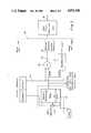
- FIG. 1is a block diagram showing the overall architecture of the microprocessor in which the present invention is currently realized.
- FIG. 2is block diagram illustrating the segmentation mechanism embodied in the microprocessor of FIG. 1.
- FIG. 3is a block diagram illustrating the page field mapping for a hit or match in the page cache memory.
- FIG. 4is a block diagram illustrating the page field mapping for no hit or match in the page cache memory of FIG. 3. For this condition, the page directory and page table in main memory are used and, hence, are shown in FIG. 4.
- FIG. 5is a diagram used to illustrate the attributes stored in the page directory, page table page cache memory.
- FIG. 6is a block diagram illustrating the organization of the content addressable memory and data storage contained within the page cache memory.
- FIG. 7is an electrical schematic of a portion of the content addressable memory of FIG. 6.
- FIG. 8is an electrical schematic fo the logic circuits associated with the detector of FIG. 6.
- the microprocessor systemincludes the micrprocessor 10 of FIG. 1.
- This microprocessoris fabricated on a single silicon substrate using complementary metal-oxide-semiconductor (CMOS) processing. Any one of many well-known CMOS processes may be employed, moreover, it will be obvious that the present invention may be realized with other technologies, for instance, n-channel, bipolar, SOS, etc.
- CMOScomplementary metal-oxide-semiconductor
- RAMrandom-access memory 13 which functions as the main memory for the system is shown in FIG. 1.
- An ordinary RAMmay be used such as one employing dynamic memories.
- the microprocessor 10has a physical address of 32-bits, and the processor itself is a 32-bit processor.
- Other components of a microprocessor system commonly usedsuch as drivers, mathematical processors, etc., are not shown in FIG. 1.
- the invented memory managementmakes use of both segmentation and paging. Segments are defined by a set of segment descriptor tables that are separate from the page tables used to describe the page translation. The two mechanisms are completely separate and independent. A virtual address is translated to a physical address in two distinct steps, using two distinct mapping mechanisms. A segmentation technique is used for the first translation step, and a paging technique is used for the second translation step. The paging translation can be turned off to produce a one-step translation with segmentation only, which is compatible with the 286.
- Segmentation(the first translation) translates a 48-bit virtual address to a 32-bit linear (intermediate) address.
- the 48-bit virtual addressis composed of a 16-bit segment selector, and a 32-bit offset within this segment.
- the 16-bit segment selectoridentifies the segment, and is used to access an entry from the segment descriptor table. This segment descriptor entry contains a base address of the segment, the size (limit) of the segment, and various attributes of the segment.
- the translation stepadds the segment base to the 32-bit offset in the virtual address to obtain a 32-bit linear address.
- the 32-bit offset in the virtual addressis compared against the segment limit, and the type of the access is checked against the segment attributes. A fault is generated and the addressing process is aborted, if the 32-bit offset is outside the segment limit, or if the type of the access is not allowed by the segment attributes.
- Paging(the second translation) translates a 32-bit linear address to a 32-bit physical address using a two-level paging table, in a process described in detail below.
- the two stepsare totally independent. This permits a (large) segment to be composed of several pages, or a page to be composed of several (small) segments.
- a segmentcan start on any boundary, and be of arbitrary size, and is not limited to starting on a page boundary, or to have a length that is an exact multiple of pages. This allows segments to describe separately protected areas of memory that start at arbitrary addresses and to be of arbitrary size.
- Segmentationcan be used to cluster a number of small segments, each with its unique protection attributes and size, into a single page.
- segmentationprovides the protection attributes
- pagingprovides a convenient method of physical memory mapping a group of related units that must be protected separately.
- Pagingcan be used to break up very large segments into small units for physical memory management. This provides a single identifier (the segment selector), and a single descriptor (the segment descriptor) for a separately protected unit of memory, rather than requiring the use of a multitude of page descriptors.
- pagingprovides an additional level of mapping that allows large segments to be mapped into separate pages that need not be contiguous in physical memory. In fact, paging allows a large segment to be mapped so that only a few pages at a time are resident in physical memory, with the remaining parts of the segment mapped onto disk.
- Pagingalso supports the definition of sub-structure within a large segment, for example, to write protect some pages of a large segment, while other pages can be written into.
- Segmentationprovides a very comprehensive protection model which works on the "natural" units used by a programmer: arbitrary sized pieces of linearly addressed memory.
- Pagingprovides the most convenient method for managing physical memory, both system main memory and backing disk memory.
- the combination of the two methods in the present inventionprovides a very flexible and powerful memory protection model.
- the microprocessorincludes a bus interface unit 14.
- the bus unitincludes buffers for permitting transmission of the 32-bit address signals and for receiving and sending the 32 bits of data.
- unit 14communicates over the internal bus 19.
- the bus unitincludes a pre-fetch unit for fetching instructions from the RAM 12 and a pre-fetch queue which communicates with the instruction unit of the instruction decode unit 16.
- the queued instructionsare processed within the execution unit 18 (arithmetic logic unit) which includes a 32-bit register file. This unit, as well as the decode unit, communicate with the internal bus 19.
- the present inventioncenters around the address translation unit 20.
- This unitprovides two functions; one associated with the segment descriptor registers, and the other with the page descriptor cache memory.
- the segment registersare for the most part known in the prior art; even so, they are described in more detail in conjunction with FIG. 2.
- the page cache memory and its interaction with the page directory and page table stored within the main memory 13is discussed in conjunction with FIGS. 3-7 and forms the basis for the present invention.
- the segmentation unit of FIG. 1receives a virtual address from the execution unit 18 and accesses the appropriate register segmentation information.
- the registercontains the segment base address which along with the offset from the virtual address are coupled over lines 23 to the page unit.
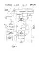
- FIG. 2illustrates the accessing of the tables in main memory when the segmentation registers are loaded with mapping information for a new segment.
- the segment fieldindexes the segment descriptor table in the main memory 13.
- the contents of the tableprovide a base address and additionally, provide attributes associated with the data in the segment.
- the base address and offsetare compared to the segment limits in comparator 27; the output of this comparator providing a fault signal.
- the adder 26which is part of the microprocessor combines the base and offset to provide a "physical" address on lines 31. This address may be used by the microprocessor as a physical address or used by the paging unit. This is done to provide compatability with certain programs written for a prior microprocessor (Intel 286). For the Intel 286, the physical address space is 24 bits.
- the page field mapping block 30which includes the page unit of FIG. 1 as well as its interaction with the page directory and page table stored in the main memory is shown in FIGS. 3 through 7.
- segmentation mechanismuses shadow registers, it also could be implemented with a cache memory as is done with the paging mechanism.
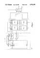
- FIG. 3the page descriptor cache memory of the page unit 22 of FIG. 1 is shown within dotted line 22a.
- This memorycomprises two arrays, a content addressable memory (CAM) 34 and a page data (base) memory 35. Both memories are implemented with static memory cells.
- CAMcontent addressable memory
- basepage data memory 35.
- Both memoriesare implemented with static memory cells.
- the organization of memories 34 and 35is described in conjunction with FIG. 6.
- the specific circuitry used for CAM 34 with its unique masking featureis described in conjunction with FIGS. 7 and 8.
- the linear address from the segment unit 21are coupled to the page unit 22 of FIG. 1. As shown in FIG. 3, this linear address comprises two fields, the page information field (20 bits) and a displacement field (12 bits). Additionally, there is a four bit page attribute field provided by the microcode. The 20-bit page information field is compared with the contents of the CAM 34. Also, the four attribute bits ("dirty”, “valid”, “U/S”, and “W/R") must also match those in the CAM before a hit occurs. (There is an exception to this when "masking" is used as will be discussed.)
- the memory 35For a hit condition, the memory 35 provides a 20-bit base word which is combined with the 12-bit displacement field of the linear address as represented by summer 36 of FIG. 3 and the resultant physical address selects from a 4k byte page frame in main memory 13.
- a page directory 13a and a page table 13bare stored in the main memory 13 (see FIG. 4).
- the base address for the page directoryis provided from the microprocessor and is shown in FIG. 4 as the page directory base 38.
- Ten bits of the page information fieldare used as an index (after being scaled by a factor of 4) into the page directory as indicated by the summer 40 in FIG. 4.
- the page directoryprovides a 32-bit word. Twenty bits of this word are used as a base for the page table.
- the other 10 bits of the page information fieldare similarly used as an index (again being scaled by factor of 4) into the page table as indicated by the summer 41.
- the page tablealso provides a 32-bit word, 20 bits of which are the page base of the physical address. This page base address is combined as indicated by summer 42 with the 12-bit displacement field to provide a 32-bit physical address.
- the stored attributes from the page directory and tableare coupled to control logic circuit 75 along with the 4 bits of attribute information associated with the linear address. Parts of this logic circuit are shown in subsequent figures are discussed in conjunction with these figures.
- FIG. 5the page directory word, page table word and CAM word are again shown.
- the protective/control attributes assigned to the four bits of the page directory wordare listed within bracket 43.
- the same four attributes with one additional attributeare used for the page table word and are set forth within bracket 44.
- the four attributes used for the CAM wordare set forth within bracket 45.
- the attributesare used for the following purpose:
- DIRTYThis bit indicates whether a page has been written into. The bit is changed once a page has been written into. This bit is used, for instance, to inform the operating system that an entire page is not "clean". This bit is stored in the page table and in the CAM (not in the page directory). The processor sets this bit in the page table when a page is written into.
- This bitis stored in only the page directory and table (not in the CAM) and is used to indicate that a page has been accessed. Once a page is accessed, this bit is changed in the memory by the processor. Unlike the dirty bit, this bit indicates whether a page has been accessed either for writing or reading.
- This read/write protection bitmust be a binary 1 to allow the page to be written into by a user level program.
- This bit in the page tableindicates if the associated page is present in the physical memory.
- This bit in the page directoryindicates if the associated page table is present in physical memory.
- VALIDThis bit which is stored only in the CAM is used to indicate if the contents of the CAM is valid. This bit is set to a first state on initialization then changed when a valid CAM word is loaded.
- the five bits from the page directory and tableare coupled to control logic circuit 75 to provide appropriate fault signals within the microprocessor.
- the user/supervisor bits from the page directory and tableare logically ANDed as indicated by gate 46 to provide the R/W bit stored in the CAM 34 of FIG. 3.
- the read/write bits from the page directory and tableare logically ANDed through gate 47 to provide the W/R bit stored in the CAM.
- the dirty bit from the page tableis stored in the CAM.
- the attributes stored in the CAMare "automatically” tested since they are treated as part of the address and matched against the four bits from the microcode. A fault condition results even if a valid page base is stored in the CAM, if, for instance, the linear address indicates that a "user" write cycle is to occur into a page with R/W0.
- the CAM 34 as shown in FIG. 6is organized in 8 sets with 4 words in each set. Twenty-one bits (17 address and 4 attributes) are used to find a match in this array.
- the four comparator lines from the four stored words in each setare connected to a detector. For instance, the comparator lines for the four words of set 1 are connected to detector 53. Similarly, the comparator linees for the four words in sets 2 through 8 are connected to detectors. The comparator lines are sensed by the detectors to determine which word in the set matches the input (21 bits) to the CAM array.
- Each of the detectorscontains "hard wired" logic which permits selection of one of the detectors depending upon the state of the 3 bits from the 20-bit page information field coupled to the detectors. (Note the other 17 bits of this bit page information field is coupled to the CAM array.)
- FIG. 6For purposes of explanation, eight detectors are implied from FIG. 6. In the current embodiment only one detector is used with the three bits selecting one set of four lines for coupling to the detector. The detector itself is shown in FIG. 8.
- the data storage portion of the cache memoryis organized into four arrays shown as arrays 35a-d.
- the data words corresponding to each set of the CAMare distributed with one word being stored in each of the four arrays. For instance, the data word (base address) selected by a hit with word 1 of set 1 is in array 35a, the data word selected by a hit with word 2 of set 1 is in array 35betc.
- the three bits used to select a detectorare also used to select a word in each of the arrays. Thus, simultaneously, words are selected from each of the four arrays.
- the final selection of a word from the arraysis done through the multiplexer 55. This multiplexer is controlled by the four comparator lines in the detector.
- the matching processwhich is a relatively slow process begins through use of the 21 bits.
- the other three bitsare able to immediately select a set of four lines and the detector is prepared for sensing a drop in potential on the comparator lines.
- all the comparator (rows) linesare precharged with the selected (hit) line remaining charged while the non-selected lines discharge.
- four words from the selected setare accessed in arrays 35a-35d. If and when a match occurs, the detector is able to identify the word within the set and this information is transmitted to the multiplexer 55 allowing the selection of the data word. This organization improves access time in the cache memory.
- FIG. 7the 21 bits which are coupled to the CAM array are again shown with 17 of the bits being coupled to the complement generator and override circuit 56 and with the 4 attribute bits coupled to the VUDW logic circuit 57.
- the 3 bits associated with the selection of the detectors described in conjunction with FIG. 6are not shown in FIG. 7.
- the circuit 56generates the true and complement signal for each of the address signals and couples them to parallel lines in the CAM array, such as lines 59 and 60.
- the VUDW logic 57generates both the true and complement signals for the attribute bits and couples them to parallel lines in the array.
- the lines 59 and 60are duplicated for each of the true and complement bit lines (i.e., 21 pairs of bit and bit/ lines).
- Each of the 32 rows in the CAM arrayhas a pair of parallel row lines such as lines 68 and 70.
- An ordinary static memory cellsuch as cell 67 is coupled between each of the bit and bit/ lines (columns) and is associated with the pair of row lines.
- the memory cellscomprise ordinary flip-flop static cells using p-channel transistors.
- One line of each pair of row lines (line 70)permits the memory cell to be coupled to the bit and bit/ line when data is written into the array. Otherwise, the content of the memory cell is compared to the data on the column lines and the results of the comparison is coupled to the hit line 68.
- the comparisonis done by comparators, one associated with each cell.
- the comparatorcomprises the n-channel transistors 61-64. Each pair of the comparator transistors, for example, transistors 61 and 62, are coupled between one side of the memory cell and the opposite bit line.
- the hit line 68is precharged through transistor 69. Then the signals coupled to the CAM are placed on the column lines. Assume first that line 59 is high. Transistor 62 does not conduct since line 60 is low. Transistor 63 does not conduct since the side of the cell to which it is connected is low. For these conditions, line 68 is not discharged, indicating that a match has occurred in the cell.
- the hit line 68provides ANDing of the comparisons occurring along the row. If a match does not occur, one or more of the comparators will cause the hit line to discharge.
- the comparatorsexamine the "binary one" condition and, in effect, ignore the "binary zero” condition. That is, for instance, if the gate of transistor 64 is high (line 59 high) then transistors 63 and 64 control the comparison. Similarly, if the bit/line 60 is high, then transistors 61 and 62 control the comparison. This feature of the comparator permits cells to be ignored. Thus, when a word is coupled to the CAM, certain bits can be masked from the matching process by making both the bit and bit/ line low. This makes it appear that the contents of the cell match the condition on the column lines. This feature is used by the VUDW logic circuit 57.
- Microcode signals coupled to logic circuit 57causes the bit and bit/ line for selected ones of the attribute bits to be low as a function of the microcode bits. This results in the attribute associated with that bit to be ignored.
- This featureis used, for instance, to ignore the U/S bit in the supervisory mode. That is, the supervisory mode can access user data. Similarly, the read/write bit can be ignored when reading or when the supervisory mode is active. The dirty bit is also ignored when reading. (The feature is not used for the valid bit.)
- the attribute bitsWhen the attribute bits are stored in main memory, they can be accessed and examined and logic circuits used to control accessing, for instance, based on the one or zero state of the U/S bit. However, with the cache memory no separate logic is used. The forcing of both the bit and bit/ lines low, in effect, provides the extra logic by allowing a match (or preventing a fault) even though the bit patterns of the attribute bits are not matched.
- the detector from FIG. 6, as shown in FIG. 8,includes a plurality of NOR gates such as gates 81, 82, 83 and 84.
- Three of the hit lines from the selected set of CAM linesare coupled to gate 81; these are shown as lines A, B, and C.
- a different combination of the linesare connected to each of the other NOR gates.
- NOR gate 84receives the hit lines D, A, and B.
- the output of each of the NOR gatesis an input to a NAND gate such as NAND gate 86.
- a hit lineprovides one input to each NAND gate. This line is the one (of the four A, B, C, D) that is not an input to the NOR gate. This is also the bit line from the set entry to be selected.
- gate 86should select the set that is associated with hit line D.
- hit line Dis coupled to the NAND gate 86.
- the hit line Cin addition to the output of gate 84, are inputs to this gate.
- An enable read signalis also coupled to the NAND gates to prevent the outputs of this logic from being enabled for a write.
- the output of the NAND gates, such as line 87,are used to control the multiplexer 55 of FIG. 6.
- the signal from the NAND gatesuch as the signal on line 87, controls the multiplexer through p-channel transistors.
- an additional inverter 88is shown with an output line 89.
- this detectorenables precharge lines to be used in the multiplexer 55. Alternately, a static arrangement could be used, but this would require considerably more power. With the arrangement as shown in FIG. 8, the output from the inverters will remain in the same state until all but one of the hit lines drop in potential. When that occurs, only a single output line will drop in potential, permitting the multiplexer to select the correct word.
- a unique address translation unitwhich uses two levels of memory management, one for segmentation and one for paging. Independent data attribute control (e.g., protection) is provided on each level.
Landscapes
- Engineering & Computer Science (AREA)
- Theoretical Computer Science (AREA)
- Physics & Mathematics (AREA)
- General Engineering & Computer Science (AREA)
- General Physics & Mathematics (AREA)
- Computer Security & Cryptography (AREA)
- Memory System Of A Hierarchy Structure (AREA)
Abstract
Description
This is a continuation of application Ser. No. 744,389, filed 06/13/85, now abandoned.
1. Field of the Invention.
The invention relates to the field of address translation units for memory management, particularly in a microprocessor system.
2. Prior Art.
There are many well-known mechanisms for memory management. In some systems, a larger address (virtual address) is translated to a smaller physical address. In others, a smaller address is used to access a larger memory space, for instance, by using bank switching. The present invention relates to the former category, that is, where larger virtual address is used to access a limited physical memory.
In memory management systems, it is also known to provide various protection mechanisms. For example, a system may prevent a user from writing into an operating system or perhaps even from reading the operating system to external ports. As will be seen, the present invention implements a protection mechanism as part of a broader control scheme which assigns "attributes" to data on two distinct levels.
The closest prior art known to Applicant is that described in U.S. Pat. No. 4,442,484. This patent describes the memory management and protection mechanism embodied in a commercially available microprocessor, the Intel 286. This microprocessor includes segmentation description registers containing segment base addresses, limit information and attributes (e.g., protection bits). The segment descriptor table and the segment descriptor registers both contain bits defining various control mechanisms such as privilege level, types of protection, etc. These control mechanisms are described in detail in U.S. Pat. No. 4,442,484.
One problem with the Intel 286 is that the segment offset is limited to 64k bytes. It also requires consecutive locations in physical memory for a segment which is not always easy to maintain. As will be seen, one advantage to the invented system is that the segment offset is as large as the physical address space. Yet, the invented system still provides compatibility with the prior segmentation mechanism found in the Intel 286. Other advantages and distinctions between the prior art system discussed in the above-mentioned patent and its commercial realization (Intel 286 microprocessor) will be apparent from the detailed description of the present invention.
An improvement to a microprocessor system which includes a microprocessor and a data memory is described. The microprocessor includes a segmentation mechanism for translating a virtual memory address to a second memory address (linear address) and for testing and controlling attributes of data memory segments. The improvement of the present invention includes a page cache memory on the microprocessor for translating a first field from the linear address for a hit or match condition. The data memory also stores page mapping data, specifically, a page directory and a page table. The first field accesses the page directory and page table if no hit occurs in the page cache memory. The output from either the page cache memory of the page table provide a physical base address for a page in memory. Another field of the linear address provides an offset within the page.
Both the page cache memory and page mapping data in the data memory store signals representing attributes of the data in a particular page. These attributes include read and write protection, indicate whether the page has been previously written into, and other information. Importantly, the page level protection provides a second tier of control over data in the memory which is separate and distinguished from the segment attributes.
FIG. 1 is a block diagram showing the overall architecture of the microprocessor in which the present invention is currently realized.
FIG. 2 is block diagram illustrating the segmentation mechanism embodied in the microprocessor of FIG. 1.
FIG. 3 is a block diagram illustrating the page field mapping for a hit or match in the page cache memory.
FIG. 4 is a block diagram illustrating the page field mapping for no hit or match in the page cache memory of FIG. 3. For this condition, the page directory and page table in main memory are used and, hence, are shown in FIG. 4.
FIG. 5 is a diagram used to illustrate the attributes stored in the page directory, page table page cache memory.
FIG. 6 is a block diagram illustrating the organization of the content addressable memory and data storage contained within the page cache memory.
FIG. 7 is an electrical schematic of a portion of the content addressable memory of FIG. 6.
FIG. 8 is an electrical schematic fo the logic circuits associated with the detector of FIG. 6.
A microprocessor system and in particular, a memory management mechanism for the system is described. In the following description, numerous specific details are set forth such as specific number of bits, etc., in order to provide a thorough understanding of the present invention. It will be obvious, however to one skilled in the art that the present invention may be practiced without these specific details. In other instances, well-known structures are not shown in detail in order not to unnecessarily obscure the present invention.
In its currently preferred embodiment, the microprocessor system includes themicrprocessor 10 of FIG. 1. This microprocessor is fabricated on a single silicon substrate using complementary metal-oxide-semiconductor (CMOS) processing. Any one of many well-known CMOS processes may be employed, moreover, it will be obvious that the present invention may be realized with other technologies, for instance, n-channel, bipolar, SOS, etc.
The memory management mechanism for some conditions requires access to tables stored in main memory. A random-access memory (RAM) 13 which functions as the main memory for the system is shown in FIG. 1. An ordinary RAM may be used such as one employing dynamic memories.
As shown in FIG. 1, themicroprocessor 10 has a physical address of 32-bits, and the processor itself is a 32-bit processor. Other components of a microprocessor system commonly used such as drivers, mathematical processors, etc., are not shown in FIG. 1.
The invented memory management makes use of both segmentation and paging. Segments are defined by a set of segment descriptor tables that are separate from the page tables used to describe the page translation. The two mechanisms are completely separate and independent. A virtual address is translated to a physical address in two distinct steps, using two distinct mapping mechanisms. A segmentation technique is used for the first translation step, and a paging technique is used for the second translation step. The paging translation can be turned off to produce a one-step translation with segmentation only, which is compatible with the 286.
Segmentation (the first translation) translates a 48-bit virtual address to a 32-bit linear (intermediate) address. The 48-bit virtual address is composed of a 16-bit segment selector, and a 32-bit offset within this segment. The 16-bit segment selector identifies the segment, and is used to access an entry from the segment descriptor table. This segment descriptor entry contains a base address of the segment, the size (limit) of the segment, and various attributes of the segment. The translation step adds the segment base to the 32-bit offset in the virtual address to obtain a 32-bit linear address. At the same time, the 32-bit offset in the virtual address is compared against the segment limit, and the type of the access is checked against the segment attributes. A fault is generated and the addressing process is aborted, if the 32-bit offset is outside the segment limit, or if the type of the access is not allowed by the segment attributes.
Paging (the second translation) translates a 32-bit linear address to a 32-bit physical address using a two-level paging table, in a process described in detail below.
The two steps are totally independent. This permits a (large) segment to be composed of several pages, or a page to be composed of several (small) segments.
A segment can start on any boundary, and be of arbitrary size, and is not limited to starting on a page boundary, or to have a length that is an exact multiple of pages. This allows segments to describe separately protected areas of memory that start at arbitrary addresses and to be of arbitrary size.
Segmentation can be used to cluster a number of small segments, each with its unique protection attributes and size, into a single page. In this case, segmentation provides the protection attributes, and paging provides a convenient method of physical memory mapping a group of related units that must be protected separately.
Paging can be used to break up very large segments into small units for physical memory management. This provides a single identifier (the segment selector), and a single descriptor (the segment descriptor) for a separately protected unit of memory, rather than requiring the use of a multitude of page descriptors. Within a segment, paging provides an additional level of mapping that allows large segments to be mapped into separate pages that need not be contiguous in physical memory. In fact, paging allows a large segment to be mapped so that only a few pages at a time are resident in physical memory, with the remaining parts of the segment mapped onto disk. Paging also supports the definition of sub-structure within a large segment, for example, to write protect some pages of a large segment, while other pages can be written into.
Segmentation provides a very comprehensive protection model which works on the "natural" units used by a programmer: arbitrary sized pieces of linearly addressed memory. Paging provides the most convenient method for managing physical memory, both system main memory and backing disk memory. The combination of the two methods in the present invention provides a very flexible and powerful memory protection model.
In FIG. 1, the microprocessor includes abus interface unit 14. The bus unit includes buffers for permitting transmission of the 32-bit address signals and for receiving and sending the 32 bits of data. Internal to the microprocessor,unit 14 communicates over theinternal bus 19. The bus unit includes a pre-fetch unit for fetching instructions from theRAM 12 and a pre-fetch queue which communicates with the instruction unit of theinstruction decode unit 16. The queued instructions are processed within the execution unit 18 (arithmetic logic unit) which includes a 32-bit register file. This unit, as well as the decode unit, communicate with theinternal bus 19.
The present invention centers around theaddress translation unit 20. This unit provides two functions; one associated with the segment descriptor registers, and the other with the page descriptor cache memory. The segment registers are for the most part known in the prior art; even so, they are described in more detail in conjunction with FIG. 2. The page cache memory and its interaction with the page directory and page table stored within themain memory 13 is discussed in conjunction with FIGS. 3-7 and forms the basis for the present invention.
The segmentation unit of FIG. 1 receives a virtual address from theexecution unit 18 and accesses the appropriate register segmentation information. The register contains the segment base address which along with the offset from the virtual address are coupled overlines 23 to the page unit.
FIG. 2 illustrates the accessing of the tables in main memory when the segmentation registers are loaded with mapping information for a new segment. The segment field indexes the segment descriptor table in themain memory 13. The contents of the table provide a base address and additionally, provide attributes associated with the data in the segment. The base address and offset are compared to the segment limits incomparator 27; the output of this comparator providing a fault signal. Theadder 26 which is part of the microprocessor combines the base and offset to provide a "physical" address onlines 31. This address may be used by the microprocessor as a physical address or used by the paging unit. This is done to provide compatability with certain programs written for a prior microprocessor (Intel 286). For the Intel 286, the physical address space is 24 bits.
The segments attributes including details on the descriptors employed such as the various privilege levels are set forth in U.S. Pat. No. 4,442,484.
The fact that the segmentation mechanism is known in the prior art is represented in FIG. 2 by the dottedline 28 which indicates the prior art structures to the left of the dotted line.
The pagefield mapping block 30 which includes the page unit of FIG. 1 as well as its interaction with the page directory and page table stored in the main memory is shown in FIGS. 3 through 7.
While in the currently preferred embodiment the segmentation mechanism uses shadow registers, it also could be implemented with a cache memory as is done with the paging mechanism.
In FIG. 3 the page descriptor cache memory of thepage unit 22 of FIG. 1 is shown within dottedline 22a. This memory comprises two arrays, a content addressable memory (CAM) 34 and a page data (base)memory 35. Both memories are implemented with static memory cells. The organization ofmemories CAM 34 with its unique masking feature is described in conjunction with FIGS. 7 and 8.
The linear address from thesegment unit 21 are coupled to thepage unit 22 of FIG. 1. As shown in FIG. 3, this linear address comprises two fields, the page information field (20 bits) and a displacement field (12 bits). Additionally, there is a four bit page attribute field provided by the microcode. The 20-bit page information field is compared with the contents of theCAM 34. Also, the four attribute bits ("dirty", "valid", "U/S", and "W/R") must also match those in the CAM before a hit occurs. (There is an exception to this when "masking" is used as will be discussed.)
For a hit condition, thememory 35 provides a 20-bit base word which is combined with the 12-bit displacement field of the linear address as represented bysummer 36 of FIG. 3 and the resultant physical address selects from a 4k byte page frame inmain memory 13.
A page directory 13a and a page table 13b are stored in the main memory 13 (see FIG. 4). The base address for the page directory is provided from the microprocessor and is shown in FIG. 4 as the page directory base 38. Ten bits of the page information field are used as an index (after being scaled by a factor of 4) into the page directory as indicated by thesummer 40 in FIG. 4. The page directory provides a 32-bit word. Twenty bits of this word are used as a base for the page table. The other 10 bits of the page information field are similarly used as an index (again being scaled by factor of 4) into the page table as indicated by thesummer 41. The page table also provides a 32-bit word, 20 bits of which are the page base of the physical address. This page base address is combined as indicated bysummer 42 with the 12-bit displacement field to provide a 32-bit physical address.
Five bits from the 12-bit fields of the page directory and table are used for attributes particularly "dirty", "access", "U/S", "R/W" and "present". These will be discussed in more detail in conjunction with FIG. 5. Remaining bits of this field are unassigned.
The stored attributes from the page directory and table are coupled to controllogic circuit 75 along with the 4 bits of attribute information associated with the linear address. Parts of this logic circuit are shown in subsequent figures are discussed in conjunction with these figures.
In FIG. 5 the page directory word, page table word and CAM word are again shown. The protective/control attributes assigned to the four bits of the page directory word are listed withinbracket 43. The same four attributes with one additional attribute are used for the page table word and are set forth withinbracket 44. The four attributes used for the CAM word are set forth withinbracket 45.
The attributes are used for the following purpose:
1. DIRTY. This bit indicates whether a page has been written into. The bit is changed once a page has been written into. This bit is used, for instance, to inform the operating system that an entire page is not "clean". This bit is stored in the page table and in the CAM (not in the page directory). The processor sets this bit in the page table when a page is written into.
2. ACCESSED. This bit is stored in only the page directory and table (not in the CAM) and is used to indicate that a page has been accessed. Once a page is accessed, this bit is changed in the memory by the processor. Unlike the dirty bit, this bit indicates whether a page has been accessed either for writing or reading.
3. U/S. The state of this bit indicates whether the contents of the page is user and supervisory accessible (binacy 1) or supervisor only (binary zero).
4. R/W. This read/write protection bit must be a binary 1 to allow the page to be written into by a user level program.
5. PRESENT. This bit in the page table indicates if the associated page is present in the physical memory. This bit in the page directory indicates if the associated page table is present in physical memory.
6. VALID. This bit which is stored only in the CAM is used to indicate if the contents of the CAM is valid. This bit is set to a first state on initialization then changed when a valid CAM word is loaded.
The five bits from the page directory and table are coupled to controllogic circuit 75 to provide appropriate fault signals within the microprocessor.
The user/supervisor bits from the page directory and table are logically ANDed as indicated bygate 46 to provide the R/W bit stored in theCAM 34 of FIG. 3. Similarly, the read/write bits from the page directory and table are logically ANDed throughgate 47 to provide the W/R bit stored in the CAM. The dirty bit from the page table is stored in the CAM. These gates are part of thecontrol logic 75 of FIG. 4.
The attributes stored in the CAM are "automatically" tested since they are treated as part of the address and matched against the four bits from the microcode. A fault condition results even if a valid page base is stored in the CAM, if, for instance, the linear address indicates that a "user" write cycle is to occur into a page with R/W0.
The ANDing of the U/S bits from the page directory and table ensures that the "worst case" is stored in the cache memory. Similarly, the ANDing of the R/W bit provides the worst case for the cache memory.
TheCAM 34 as shown in FIG. 6 is organized in 8 sets with 4 words in each set. Twenty-one bits (17 address and 4 attributes) are used to find a match in this array. The four comparator lines from the four stored words in each set are connected to a detector. For instance, the comparator lines for the four words ofset 1 are connected todetector 53. Similarly, the comparator linees for the four words in sets 2 through 8 are connected to detectors. The comparator lines are sensed by the detectors to determine which word in the set matches the input (21 bits) to the CAM array. Each of the detectors contains "hard wired" logic which permits selection of one of the detectors depending upon the state of the 3 bits from the 20-bit page information field coupled to the detectors. (Note the other 17 bits of this bit page information field is coupled to the CAM array.)
For purposes of explanation, eight detectors are implied from FIG. 6. In the current embodiment only one detector is used with the three bits selecting one set of four lines for coupling to the detector. The detector itself is shown in FIG. 8.
The data storage portion of the cache memory is organized into four arrays shown as arrays 35a-d. The data words corresponding to each set of the CAM are distributed with one word being stored in each of the four arrays. For instance, the data word (base address) selected by a hit withword 1 ofset 1 is in array 35a, the data word selected by a hit with word 2 ofset 1 is in array 35betc. The three bits used to select a detector are also used to select a word in each of the arrays. Thus, simultaneously, words are selected from each of the four arrays. The final selection of a word from the arrays is done through themultiplexer 55. This multiplexer is controlled by the four comparator lines in the detector.
When the memory cache is accessed, the matching process which is a relatively slow process begins through use of the 21 bits. The other three bits are able to immediately select a set of four lines and the detector is prepared for sensing a drop in potential on the comparator lines. (As will be discussed, all the comparator (rows) lines are precharged with the selected (hit) line remaining charged while the non-selected lines discharge.) Simultaneously, four words from the selected set are accessed in arrays 35a-35d. If and when a match occurs, the detector is able to identify the word within the set and this information is transmitted to themultiplexer 55 allowing the selection of the data word. This organization improves access time in the cache memory.
In FIG. 7, the 21 bits which are coupled to the CAM array are again shown with 17 of the bits being coupled to the complement generator and override circuit 56 and with the 4 attribute bits coupled to theVUDW logic circuit 57. The 3 bits associated with the selection of the detectors described in conjunction with FIG. 6 are not shown in FIG. 7.
The circuit 56 generates the true and complement signal for each of the address signals and couples them to parallel lines in the CAM array, such aslines VUDW logic 57 generates both the true and complement signals for the attribute bits and couples them to parallel lines in the array. Thelines
Each of the 32 rows in the CAM array has a pair of parallel row lines such aslines cell 67 is coupled between each of the bit and bit/ lines (columns) and is associated with the pair of row lines. In the presently preferred embodiment, the memory cells comprise ordinary flip-flop static cells using p-channel transistors. One line of each pair of row lines (line 70) permits the memory cell to be coupled to the bit and bit/ line when data is written into the array. Otherwise, the content of the memory cell is compared to the data on the column lines and the results of the comparison is coupled to the hitline 68. The comparison is done by comparators, one associated with each cell. The comparator comprises the n-channel transistors 61-64. Each pair of the comparator transistors, for example,transistors
Assume that data is stored in thememory cell 67 and that the node of the cell closest to bitline 59 is high. When the contents of the CAM are examined, first thehit line 68 is precharged throughtransistor 69. Then the signals coupled to the CAM are placed on the column lines. Assume first thatline 59 is high.Transistor 62 does not conduct sinceline 60 is low.Transistor 63 does not conduct since the side of the cell to which it is connected is low. For these conditions,line 68 is not discharged, indicating that a match has occurred in the cell. The hitline 68 provides ANDing of the comparisons occurring along the row. If a match does not occur, one or more of the comparators will cause the hit line to discharge.
During precharging thecircuits 56 and 57 generate an override signal causing all column lines (both bit and bit/) to be low. This prevents the comparators from draining the charge from the hit lines before the comparison begins.
It should be noted that the comparators examine the "binary one" condition and, in effect, ignore the "binary zero" condition. That is, for instance, if the gate oftransistor 64 is high (line 59 high) thentransistors line 60 is high, thentransistors VUDW logic circuit 57.
Microcode signals coupled tologic circuit 57 causes the bit and bit/ line for selected ones of the attribute bits to be low as a function of the microcode bits. This results in the attribute associated with that bit to be ignored. This feature is used, for instance, to ignore the U/S bit in the supervisory mode. That is, the supervisory mode can access user data. Similarly, the read/write bit can be ignored when reading or when the supervisory mode is active. The dirty bit is also ignored when reading. (The feature is not used for the valid bit.)
When the attribute bits are stored in main memory, they can be accessed and examined and logic circuits used to control accessing, for instance, based on the one or zero state of the U/S bit. However, with the cache memory no separate logic is used. The forcing of both the bit and bit/ lines low, in effect, provides the extra logic by allowing a match (or preventing a fault) even though the bit patterns of the attribute bits are not matched.
The detector from FIG. 6, as shown in FIG. 8, includes a plurality of NOR gates such asgates gate 81; these are shown as lines A, B, and C. A different combination of the lines are connected to each of the other NOR gates. For instance, NORgate 84 receives the hit lines D, A, and B. The output of each of the NOR gates is an input to a NAND gate such asNAND gate 86. A hit line provides one input to each NAND gate. This line is the one (of the four A, B, C, D) that is not an input to the NOR gate. This is also the bit line from the set entry to be selected. For example,gate 86 should select the set that is associated with hit line D. For instance, in the case of NORgate 81, hit line D is coupled to theNAND gate 86. Similarly, for theNAND gate 90, the hit line C in addition to the output ofgate 84, are inputs to this gate. An enable read signal is also coupled to the NAND gates to prevent the outputs of this logic from being enabled for a write. The output of the NAND gates, such asline 87, are used to control themultiplexer 55 of FIG. 6. In practice, the signal from the NAND gate, such as the signal online 87, controls the multiplexer through p-channel transistors. For purposes of explanation, anadditional inverter 88 is shown with anoutput line 89.
The advantage to this detector is that it enables precharge lines to be used in themultiplexer 55. Alternately, a static arrangement could be used, but this would require considerably more power. With the arrangement as shown in FIG. 8, the output from the inverters will remain in the same state until all but one of the hit lines drop in potential. When that occurs, only a single output line will drop in potential, permitting the multiplexer to select the correct word.
thus, a unique address translation unit has been described which uses two levels of memory management, one for segmentation and one for paging. Independent data attribute control (e.g., protection) is provided on each level.
Claims (7)
1. A microprocessor device comprising:
(a) address register means for providing virtual memory addresses;
(b) a bus interface unit providing an interface to address terminals and data terminals of said device;
(c) an address translation unit receiving said virtual memory addresses from said address register means, the address translation unit including:
(i) a segmentation unit having at least one segment descriptor registor storing a segment base address and a limit; a comparator in said segmentation unit comparing said virtual address to said limit and generating a fault if said limit is exceeded, said limit being of variable size; the segmentation unit adding said segment base address to said virtual address to produce a linear address having a page information field and an offset;
(ii) a page cache for storing a plurality of page entries and tags for said page entries, said page entries representing memory addresses for pages of fixed size; means for comparing tags to said page information field of said linear address to produce a match indication, the page cache producing a page entry output corresponding to one of said page entries if the match indication occurs;
(iii) page table addressing means responsive to said match indication and, if the match indication does not indicate a match, generating a page table address from a page base address and at least part of said page information field for transfer to said bus interface unit; the page table addressing means receiving a page table entry from said but interface unit in response to said page table address, the page table entry corresponding to one of said page entries; and
(d) address generating means connected, in the alternative, to receive either (i) said linear address from said segmentation unit, or (ii) said offset part of said linear address combined with either said page entry output from said page cache or said page table entry from said page table addressing means; said address generating means producing a physical address for applying to said bus interface unit.
2. A device according to claim 1 combined with a memory external to said device storing said page table entries and accessed by said physical address received from said terminals of said device.
3. A device according to claim 1 wherein said limit has a maximum value equal to an address range addressable by bits in said virtual address.
4. A device according to claim 1 wherein said limit may be larger than or smaller than said fixed page size.
5. A device according to claim 1 wherein said segment descriptor register stores said segment base address, said segment descriptor register further storing attributes of a segment of memory, said attributes including the type of use allowed for locations in said segment of memory and a privilege level for access to said segment of memory.
6. A device according to claim 2 wherin said memory also stores a plurality of segment descriptors for transfer to said segment descriptor register.
7. A device according to claim 1 wherein said page table addressing means generates a first page table address from said page base address and a first part of said page information field, for transfer of the first page table address to said bus interface unit; and wherein said page table addressing means generates a second page table address from a second page base address received from said bus interface unit and a second part of said page information field, for transfer of said second page table address to said bus interface unit.
Priority Applications (2)
| Application Number | Priority Date | Filing Date | Title |
|---|---|---|---|
| US07/185,325US4972338A (en) | 1985-06-13 | 1988-04-19 | Memory management for microprocessor system |
| US07/506,211US5321836A (en) | 1985-06-13 | 1990-04-09 | Virtual memory management method and apparatus utilizing separate and independent segmentation and paging mechanism |
Applications Claiming Priority (2)
| Application Number | Priority Date | Filing Date | Title |
|---|---|---|---|
| US74438985A | 1985-06-13 | 1985-06-13 | |
| US07/185,325US4972338A (en) | 1985-06-13 | 1988-04-19 | Memory management for microprocessor system |
Related Parent Applications (1)
| Application Number | Title | Priority Date | Filing Date |
|---|---|---|---|
| US74438985AContinuation | 1985-06-13 | 1985-06-13 |
Related Child Applications (1)
| Application Number | Title | Priority Date | Filing Date |
|---|---|---|---|
| US07/506,211ContinuationUS5321836A (en) | 1985-06-13 | 1990-04-09 | Virtual memory management method and apparatus utilizing separate and independent segmentation and paging mechanism |
Publications (1)
| Publication Number | Publication Date |
|---|---|
| US4972338Atrue US4972338A (en) | 1990-11-20 |
Family
ID=26881042
Family Applications (2)
| Application Number | Title | Priority Date | Filing Date |
|---|---|---|---|
| US07/185,325Expired - LifetimeUS4972338A (en) | 1985-06-13 | 1988-04-19 | Memory management for microprocessor system |
| US07/506,211Expired - LifetimeUS5321836A (en) | 1985-06-13 | 1990-04-09 | Virtual memory management method and apparatus utilizing separate and independent segmentation and paging mechanism |
Family Applications After (1)
| Application Number | Title | Priority Date | Filing Date |
|---|---|---|---|
| US07/506,211Expired - LifetimeUS5321836A (en) | 1985-06-13 | 1990-04-09 | Virtual memory management method and apparatus utilizing separate and independent segmentation and paging mechanism |
Country Status (1)
| Country | Link |
|---|---|
| US (2) | US4972338A (en) |
Cited By (80)
| Publication number | Priority date | Publication date | Assignee | Title |
|---|---|---|---|---|
| US5123095A (en)* | 1989-01-17 | 1992-06-16 | Ergo Computing, Inc. | Integrated scalar and vector processors with vector addressing by the scalar processor |
| US5239635A (en)* | 1988-06-06 | 1993-08-24 | Digital Equipment Corporation | Virtual address to physical address translation using page tables in virtual memory |
| US5255377A (en)* | 1989-11-13 | 1993-10-19 | Intel Corporation | Interface for arbitrating access to the paging unit of a computer processor |
| US5263140A (en)* | 1991-01-23 | 1993-11-16 | Silicon Graphics, Inc. | Variable page size per entry translation look-aside buffer |
| US5282201A (en)* | 1987-12-22 | 1994-01-25 | Kendall Square Research Corporation | Dynamic packet routing network |
| US5297265A (en)* | 1987-12-22 | 1994-03-22 | Kendall Square Research Corporation | Shared memory multiprocessor system and method of operation thereof |
| US5313647A (en)* | 1991-09-20 | 1994-05-17 | Kendall Square Research Corporation | Digital data processor with improved checkpointing and forking |
| US5321836A (en)* | 1985-06-13 | 1994-06-14 | Intel Corporation | Virtual memory management method and apparatus utilizing separate and independent segmentation and paging mechanism |
| US5327540A (en)* | 1991-09-18 | 1994-07-05 | Ncr Corporation | Method and apparatus for decoding bus master arbitration levels to optimize memory transfers |
| US5335325A (en)* | 1987-12-22 | 1994-08-02 | Kendall Square Research Corporation | High-speed packet switching apparatus and method |
| US5341483A (en)* | 1987-12-22 | 1994-08-23 | Kendall Square Research Corporation | Dynamic hierarchial associative memory |
| US5428759A (en)* | 1992-03-30 | 1995-06-27 | Unisys Corporation | Associative memory system having segment and page descriptor content-addressable memories |
| US5440710A (en)* | 1994-03-08 | 1995-08-08 | Exponential Technology, Inc. | Emulation of segment bounds checking using paging with sub-page validity |
| WO1995022795A3 (en)* | 1994-02-08 | 1995-09-08 | Meridian Semiconductor Inc | Method and apparatus for detecting memory segment violations in a computer system |
| US5469556A (en)* | 1989-12-12 | 1995-11-21 | Harris Corporation | Resource access security system for controlling access to resources of a data processing system |
| US5473348A (en)* | 1992-06-09 | 1995-12-05 | Kabushiki Kaisha Toshiba | Apparatus and method of controlling paging unit of coprocessor built in display control system |
| US5530824A (en)* | 1994-04-04 | 1996-06-25 | Motorola, Inc. | Address translation circuit |
| US5530822A (en)* | 1994-04-04 | 1996-06-25 | Motorola, Inc. | Address translator and method of operation |
| US5535393A (en)* | 1991-09-20 | 1996-07-09 | Reeve; Christopher L. | System for parallel processing that compiles a filed sequence of instructions within an iteration space |
| US5535351A (en)* | 1994-04-04 | 1996-07-09 | Motorola, Inc. | Address translator with by-pass circuit and method of operation |
| US5537559A (en)* | 1994-02-08 | 1996-07-16 | Meridian Semiconductor, Inc. | Exception handling circuit and method |
| US5583806A (en)* | 1994-10-17 | 1996-12-10 | Advanced Micro Devices, Inc. | Optimized binary adder for concurrently generating effective and intermediate addresses |
| US5586291A (en)* | 1994-12-23 | 1996-12-17 | Emc Corporation | Disk controller with volatile and non-volatile cache memories |
| US5604879A (en)* | 1994-04-04 | 1997-02-18 | Motorola Inc. | Single array address translator with segment and page invalidate ability and method of operation |
| US5617554A (en)* | 1992-02-10 | 1997-04-01 | Intel Corporation | Physical address size selection and page size selection in an address translator |
| US5652872A (en)* | 1994-03-08 | 1997-07-29 | Exponential Technology, Inc. | Translator having segment bounds encoding for storage in a TLB |
| US5666508A (en)* | 1995-06-07 | 1997-09-09 | Texas Instruments Incorporated | Four state two bit recoded alignment fault state circuit for microprocessor address misalignment fault generation |
| US5680578A (en)* | 1995-06-07 | 1997-10-21 | Advanced Micro Devices, Inc. | Microprocessor using an instruction field to specify expanded functionality and a computer system employing same |
| US5684993A (en)* | 1993-01-04 | 1997-11-04 | Microsoft Corporation | Segregation of thread-specific information from shared task information |
| US5737752A (en)* | 1993-04-08 | 1998-04-07 | International Computers Limited | Cache replacement mechanism |
| US5749087A (en)* | 1996-07-30 | 1998-05-05 | International Business Machines Corporation | Method and apparatus for maintaining n-way associative directories utilizing a content addressable memory |
| US5752264A (en)* | 1995-03-31 | 1998-05-12 | International Business Machines Corporation | Computer architecture incorporating processor clusters and hierarchical cache memories |
| US5752275A (en)* | 1995-03-31 | 1998-05-12 | Intel Corporation | Translation look-aside buffer including a single page size translation unit |
| US5761413A (en)* | 1987-12-22 | 1998-06-02 | Sun Microsystems, Inc. | Fault containment system for multiprocessor with shared memory |
| US5768574A (en)* | 1995-06-07 | 1998-06-16 | Advanced Micro Devices, Inc. | Microprocessor using an instruction field to expand the condition flags and a computer system employing the microprocessor |
| US5787486A (en)* | 1995-12-15 | 1998-07-28 | International Business Machines Corporation | Bus protocol for locked cycle cache hit |
| US5819080A (en)* | 1996-01-02 | 1998-10-06 | Advanced Micro Devices, Inc. | Microprocessor using an instruction field to specify condition flags for use with branch instructions and a computer system employing the microprocessor |
| US5822786A (en)* | 1994-11-14 | 1998-10-13 | Advanced Micro Devices, Inc. | Apparatus and method for determining if an operand lies within an expand up or expand down segment |
| US5822578A (en)* | 1987-12-22 | 1998-10-13 | Sun Microsystems, Inc. | System for inserting instructions into processor instruction stream in order to perform interrupt processing |
| US5822778A (en)* | 1995-06-07 | 1998-10-13 | Advanced Micro Devices, Inc. | Microprocessor and method of using a segment override prefix instruction field to expand the register file |
| US5852607A (en)* | 1997-02-26 | 1998-12-22 | Cisco Technology, Inc. | Addressing mechanism for multiple look-up tables |
| US5895489A (en)* | 1991-10-16 | 1999-04-20 | Intel Corporation | Memory management system including an inclusion bit for maintaining cache coherency |
| US5946715A (en)* | 1994-09-23 | 1999-08-31 | Ati Technologies Inc. | Page address space with varying page size and boundaries |
| US5956751A (en)* | 1995-06-28 | 1999-09-21 | Industrial Technology Research Institute | Computer memory management system using physical segmentation space allocation |
| US5974525A (en)* | 1997-12-05 | 1999-10-26 | Intel Corporation | System for allowing multiple instructions to use the same logical registers by remapping them to separate physical segment registers when the first is being utilized |
| US5978900A (en)* | 1996-12-30 | 1999-11-02 | Intel Corporation | Renaming numeric and segment registers using common general register pool |
| US5987584A (en)* | 1996-09-17 | 1999-11-16 | Vlsi Technology, Inc. | Wavetable address cache to reduce accesses over a PCI bus |
| US6047365A (en)* | 1996-09-17 | 2000-04-04 | Vlsi Technology, Inc. | Multiple entry wavetable address cache to reduce accesses over a PCI bus |
| US6049897A (en)* | 1997-01-07 | 2000-04-11 | Intel Corporation | Multiple segment register use with different operand size |
| US6157996A (en)* | 1997-11-13 | 2000-12-05 | Advanced Micro Devices, Inc. | Processor programably configurable to execute enhanced variable byte length instructions including predicated execution, three operand addressing, and increased register space |
| US6178550B1 (en)* | 1995-01-31 | 2001-01-23 | Dell Usa | Mechanism for optimizing location of machine-dependent code |
| US6230259B1 (en) | 1997-10-31 | 2001-05-08 | Advanced Micro Devices, Inc. | Transparent extended state save |
| US20020066792A1 (en)* | 2000-12-06 | 2002-06-06 | Mobile-Mind, Inc. | Concurrent communication with multiple applications on a smart card |
| US6418524B1 (en) | 1999-12-28 | 2002-07-09 | Ati International Srl | Method and apparatus for dependent segmentation and paging processing |
| US6446034B1 (en)* | 1998-12-16 | 2002-09-03 | Bull Hn Information Systems Inc. | Processor emulation virtual memory address translation |
| US20030014667A1 (en)* | 2001-07-16 | 2003-01-16 | Andrei Kolichtchak | Buffer overflow attack detection and suppression |
| US20030177298A1 (en)* | 2002-02-08 | 2003-09-18 | Dan Kaiser | Dynamic executable code and data image address extension |
| US6804754B1 (en)* | 1997-05-21 | 2004-10-12 | International Business Machines Corporation | Space management in compressed main memory |
| KR100455116B1 (en)* | 1997-10-23 | 2004-12-30 | 엘지전자 주식회사 | How to Access Memory in an Embedded System |
| US6877084B1 (en) | 2000-08-09 | 2005-04-05 | Advanced Micro Devices, Inc. | Central processing unit (CPU) accessing an extended register set in an extended register mode |
| US6981132B2 (en) | 2000-08-09 | 2005-12-27 | Advanced Micro Devices, Inc. | Uniform register addressing using prefix byte |
| US20060136694A1 (en)* | 2004-12-17 | 2006-06-22 | Robert Hasbun | Techniques to partition physical memory |
| US7310706B1 (en) | 2001-06-01 | 2007-12-18 | Mips Technologies, Inc. | Random cache line refill |
| US20090182964A1 (en)* | 2008-01-11 | 2009-07-16 | International Business Machines Corporation | Dynamic address translation with format control |
| US20090182971A1 (en)* | 2008-01-11 | 2009-07-16 | International Business Machines Corporation | Dynamic address translation with fetch protection |
| US20090182974A1 (en)* | 2008-01-11 | 2009-07-16 | International Business Machines Corporation | Dynamic address translation with access control |
| WO2009087135A1 (en)* | 2008-01-11 | 2009-07-16 | International Business Machines Corporation | Dynamic address translation with dat protection |
| US20090182966A1 (en)* | 2008-01-11 | 2009-07-16 | International Business Machines Corporation | Dynamic address translation with frame management |
| US20090182975A1 (en)* | 2008-01-11 | 2009-07-16 | International Business Machines Corporation | Dynamic address translation with load page table entry address |
| US20090182973A1 (en)* | 2008-01-11 | 2009-07-16 | International Business Machines Corporation | Dynamic address translation with load real address |
| US20090182972A1 (en)* | 2008-01-11 | 2009-07-16 | International Business Machines Corporation | Dynamic address translation with format control |
| US20090187724A1 (en)* | 2008-01-11 | 2009-07-23 | International Business Machines Corporation | Dynamic address translation with frame management |
| US20090193214A1 (en)* | 2008-01-11 | 2009-07-30 | International Business Machines Corporation | Dynamic address translation with frame management |
| US20090216984A1 (en)* | 2008-02-25 | 2009-08-27 | International Business Machines Corporation | Optimizations of a perform frame management function issued by pageable guests |
| US20090216992A1 (en)* | 2008-02-26 | 2009-08-27 | International Business Machines Corporation | Dynamic address translation with translation exception qualifier |
| US8117417B2 (en) | 2008-01-11 | 2012-02-14 | International Business Machines Corporation | Dynamic address translation with change record override |
| US8612721B2 (en) | 2010-09-22 | 2013-12-17 | Kabushiki Kaisha Toshiba | Semiconductor memory controlling device |
| US8930672B2 (en) | 2010-10-08 | 2015-01-06 | Snu R&Db Foundation | Multiprocessor using a shared virtual memory and method of generating a translation table |
| US20160364338A1 (en)* | 2015-06-12 | 2016-12-15 | Intel Corporation | Supporting secure memory intent |
| EP3767481A1 (en) | 2019-07-19 | 2021-01-20 | PLS Patent-, Lizenz- und Schutzrechte Verwertung GmbH | Processor |
Families Citing this family (50)
| Publication number | Priority date | Publication date | Assignee | Title |
|---|---|---|---|---|
| US5509131A (en)* | 1991-10-22 | 1996-04-16 | Unisys Corporation | System for pointer updating across paged memory |
| US5675762A (en)* | 1992-04-03 | 1997-10-07 | International Business Machines Corporation | System for locking down part of portion of memory and updating page directory with entry corresponding to part of portion of the memory locked down |
| US5555395A (en)* | 1993-05-28 | 1996-09-10 | Dell U.S.A. L.P. | System for memory table cache reloads in a reduced number of cycles using a memory controller to set status bits in the main memory table |
| EP0651332B1 (en)* | 1993-10-29 | 2001-07-18 | Advanced Micro Devices, Inc. | Linearly addressable microprocessor cache |
| US5623636A (en)* | 1993-11-09 | 1997-04-22 | Motorola Inc. | Data processing system and method for providing memory access protection using transparent translation registers and default attribute bits |
| US5590297A (en)* | 1994-01-04 | 1996-12-31 | Intel Corporation | Address generation unit with segmented addresses in a mircroprocessor |
| US5590351A (en)* | 1994-01-21 | 1996-12-31 | Advanced Micro Devices, Inc. | Superscalar execution unit for sequential instruction pointer updates and segment limit checks |
| US5564030A (en)* | 1994-02-08 | 1996-10-08 | Meridian Semiconductor, Inc. | Circuit and method for detecting segment limit errors for code fetches |
| US5577219A (en)* | 1994-05-02 | 1996-11-19 | Intel Corporation | Method and apparatus for preforming memory segment limit violation checks |
| US5754817A (en)* | 1994-09-29 | 1998-05-19 | Intel Corporation | Execution in place of a file stored non-contiguously in a non-volatile memory |
| US5895503A (en)* | 1995-06-02 | 1999-04-20 | Belgard; Richard A. | Address translation method and mechanism using physical address information including during a segmentation process |
| US6813699B1 (en) | 1995-06-02 | 2004-11-02 | Transmeta Corporation | Speculative address translation for processor using segmentation and optional paging |
| US6041396A (en)* | 1996-03-14 | 2000-03-21 | Advanced Micro Devices, Inc. | Segment descriptor cache addressed by part of the physical address of the desired descriptor |
| US6542919B1 (en)* | 1996-03-22 | 2003-04-01 | Koninklijke Philips Electronics N.V. | Operating system for use with protection domains in a single address space |
| US5970512A (en)* | 1997-03-27 | 1999-10-19 | International Business Machines Corporation | Translation shadow array adder-decoder circuit for selecting consecutive TLB entries |
| US5920881A (en)* | 1997-05-20 | 1999-07-06 | Micron Electronics, Inc. | Method and system for using a virtual register file in system memory |
| US6249853B1 (en) | 1997-06-25 | 2001-06-19 | Micron Electronics, Inc. | GART and PTES defined by configuration registers |
| US6069638A (en)* | 1997-06-25 | 2000-05-30 | Micron Electronics, Inc. | System for accelerated graphics port address remapping interface to main memory |
| US6282625B1 (en) | 1997-06-25 | 2001-08-28 | Micron Electronics, Inc. | GART and PTES defined by configuration registers |
| US6192457B1 (en) | 1997-07-02 | 2001-02-20 | Micron Technology, Inc. | Method for implementing a graphic address remapping table as a virtual register file in system memory |
| US6195734B1 (en) | 1997-07-02 | 2001-02-27 | Micron Technology, Inc. | System for implementing a graphic address remapping table as a virtual register file in system memory |
| US6115790A (en)* | 1997-08-29 | 2000-09-05 | Silicon Graphics, Inc. | System, method and computer program product for organizing page caches |
| US6237059B1 (en) | 1997-11-26 | 2001-05-22 | Compaq Computer Corporation | Method for estimating statistics of properties of memory system interactions among contexts in a computer system |
| US6175814B1 (en) | 1997-11-26 | 2001-01-16 | Compaq Computer Corporation | Apparatus for determining the instantaneous average number of instructions processed |
| US6442585B1 (en) | 1997-11-26 | 2002-08-27 | Compaq Computer Corporation | Method for scheduling contexts based on statistics of memory system interactions in a computer system |
| US6332178B1 (en) | 1997-11-26 | 2001-12-18 | Compaq Computer Corporation | Method for estimating statistics of properties of memory system transactions |
| US6195748B1 (en) | 1997-11-26 | 2001-02-27 | Compaq Computer Corporation | Apparatus for sampling instruction execution information in a processor pipeline |
| US6549930B1 (en) | 1997-11-26 | 2003-04-15 | Compaq Computer Corporation | Method for scheduling threads in a multithreaded processor |
| US6163840A (en)* | 1997-11-26 | 2000-12-19 | Compaq Computer Corporation | Method and apparatus for sampling multiple potentially concurrent instructions in a processor pipeline |
| US6237073B1 (en) | 1997-11-26 | 2001-05-22 | Compaq Computer Corporation | Method for providing virtual memory to physical memory page mapping in a computer operating system that randomly samples state information |
| US6374367B1 (en) | 1997-11-26 | 2002-04-16 | Compaq Computer Corporation | Apparatus and method for monitoring a computer system to guide optimization |
| US6157398A (en)* | 1997-12-30 | 2000-12-05 | Micron Technology, Inc. | Method of implementing an accelerated graphics port for a multiple memory controller computer system |
| US7071946B2 (en)* | 1997-12-30 | 2006-07-04 | Micron Technology, Inc. | Accelerated graphics port for a multiple memory controller computer system |
| US6252612B1 (en) | 1997-12-30 | 2001-06-26 | Micron Electronics, Inc. | Accelerated graphics port for multiple memory controller computer system |
| US6272576B1 (en) | 1998-01-20 | 2001-08-07 | Micron Technology, Inc. | Method for extending the available number of configuration registers |
| US6243775B1 (en) | 1998-01-20 | 2001-06-05 | Micron Technology, Inc. | System for extending the available number of configuration registers |
| US6108733A (en)* | 1998-01-20 | 2000-08-22 | Micron Technology, Inc. | Method for extending the available number of configuration registers |
| US6405267B1 (en)* | 1999-01-22 | 2002-06-11 | S3 Graphics Co., Ltd. | Command reordering for out of order bus transfer |
| US6298427B1 (en) | 1999-01-26 | 2001-10-02 | Dell Usa, L.P. | Method and apparatus for mapping hard disk partitions and block devices to logical drives in a computer system |
| US6665785B1 (en) | 2000-10-19 | 2003-12-16 | International Business Machines, Corporation | System and method for automating page space optimization |
| US6832304B2 (en) | 2002-01-17 | 2004-12-14 | Dell Products L.P. | System, method and computer program product for mapping system memory in a multiple node information handling system |
| US7146457B2 (en)* | 2003-09-24 | 2006-12-05 | Hewlett-Packard Development Company, L.P. | Content addressable memory selectively addressable in a physical address mode and a virtual address mode |
| US7107431B2 (en)* | 2004-02-19 | 2006-09-12 | International Business Machines Corporation | Apparatus and method for lazy segment promotion for pre-translated segments |
| US7117337B2 (en)* | 2004-02-19 | 2006-10-03 | International Business Machines Corporation | Apparatus and method for providing pre-translated segments for page translations in segmented operating systems |
| US7404064B2 (en)* | 2004-04-07 | 2008-07-22 | Stmicroelectronics S.A. | Method and device for calculating addresses of a segmented program memory |
| US8112618B2 (en) | 2004-04-08 | 2012-02-07 | Texas Instruments Incorporated | Less-secure processors, integrated circuits, wireless communications apparatus, methods and processes of making |
| EP1870814B1 (en) | 2006-06-19 | 2014-08-13 | Texas Instruments France | Method and apparatus for secure demand paging for processor devices |
| EP1870813B1 (en)* | 2006-06-19 | 2013-01-30 | Texas Instruments France | Page processing circuits, devices, methods and systems for secure demand paging and other operations |
| US8327085B2 (en) | 2010-05-05 | 2012-12-04 | International Business Machines Corporation | Characterizing multiple resource utilization using a relationship model to optimize memory utilization in a virtual machine environment |
| US9858198B2 (en) | 2015-06-26 | 2018-01-02 | Intel Corporation | 64KB page system that supports 4KB page operations |
Citations (16)
| Publication number | Priority date | Publication date | Assignee | Title |
|---|---|---|---|---|
| GB1595740A (en)* | 1978-05-25 | 1981-08-19 | Fujitsu Ltd | Data processing apparatus |
| US4377855A (en)* | 1980-11-06 | 1983-03-22 | National Semiconductor Corporation | Content-addressable memory |
| US4432053A (en)* | 1981-06-29 | 1984-02-14 | Burroughs Corporation | Address generating apparatus and method |
| US4441155A (en)* | 1981-11-23 | 1984-04-03 | International Business Machines Corporation | Page controlled cache directory addressing |
| US4442484A (en)* | 1980-10-14 | 1984-04-10 | Intel Corporation | Microprocessor memory management and protection mechanism |
| US4458310A (en)* | 1981-10-02 | 1984-07-03 | At&T Bell Laboratories | Cache memory using a lowest priority replacement circuit |
| EP0113240A2 (en)* | 1982-12-30 | 1984-07-11 | International Business Machines Corporation | Virtual memory address translation mechanism with controlled data persistence |
| US4523301A (en)* | 1982-06-04 | 1985-06-11 | Matsushita Electric Industrial Co., Ltd. | Associative memory |
| US4612612A (en)* | 1983-08-30 | 1986-09-16 | Amdahl Corporation | Virtually addressed cache |
| US4631660A (en)* | 1983-08-30 | 1986-12-23 | Amdahl Corporation | Addressing system for an associative cache memory |
| US4646271A (en)* | 1983-12-23 | 1987-02-24 | Hitachi, Ltd. | Content addressable memory having dual access modes |
| US4654777A (en)* | 1982-05-25 | 1987-03-31 | Tokyo Shibaura Denki Kabushiki Kaisha | Segmented one and two level paging address translation system |
| US4656626A (en)* | 1984-12-14 | 1987-04-07 | Itt Corporation | Apparatus and method for providing dynamically assigned switch paths |
| US4669043A (en)* | 1984-02-17 | 1987-05-26 | Signetics Corporation | Memory access controller |
| US4763250A (en)* | 1985-04-01 | 1988-08-09 | Motorola, Inc. | Paged memory management unit having variable number of translation table levels |
| US4785398A (en)* | 1985-12-19 | 1988-11-15 | Honeywell Bull Inc. | Virtual cache system using page level number generating CAM to access other memories for processing requests relating to a page |
Family Cites Families (75)
| Publication number | Priority date | Publication date | Assignee | Title |
|---|---|---|---|---|
| US3047228A (en)* | 1957-03-30 | 1962-07-31 | Bauer Friedrich Ludwig | Automatic computing machines and method of operation |
| US3292152A (en)* | 1962-09-17 | 1966-12-13 | Burroughs Corp | Memory |
| CA784373A (en)* | 1963-04-01 | 1968-04-30 | W. Bremer John | Content addressed memory system |
| DE1181461B (en)* | 1963-10-08 | 1964-11-12 | Telefunken Patent | Address adder of a program-controlled calculating machine |
| US3298001A (en)* | 1964-05-04 | 1967-01-10 | Gen Electric | Data processing unit for providing selective memory addressing by external apparatus |
| US3351913A (en)* | 1964-10-21 | 1967-11-07 | Gen Electric | Memory system including means for selectively altering or not altering restored data |
| US3370274A (en)* | 1964-12-30 | 1968-02-20 | Bell Telephone Labor Inc | Data processor control utilizing tandem signal operations |
| FR1509022A (en)* | 1965-11-26 | 1968-03-25 | ||
| US3412382A (en)* | 1965-11-26 | 1968-11-19 | Massachusetts Inst Technology | Shared-access data processing system |
| US3425039A (en)* | 1966-06-27 | 1969-01-28 | Gen Electric | Data processing system employing indirect character addressing capability |
| US3454931A (en)* | 1966-06-27 | 1969-07-08 | Gen Electric | Data processing system including address development apparatus |
| US3473159A (en)* | 1966-07-07 | 1969-10-14 | Gen Electric | Data processing system including means for protecting predetermined areas of memory |
| US3479649A (en)* | 1966-07-22 | 1969-11-18 | Gen Electric | Data processing system including means for masking program interrupt requests |
| US3510847A (en)* | 1967-09-25 | 1970-05-05 | Burroughs Corp | Address manipulation circuitry for a digital computer |
| US3546677A (en)* | 1967-10-02 | 1970-12-08 | Burroughs Corp | Data processing system having tree structured stack implementation |
| US3548384A (en)* | 1967-10-02 | 1970-12-15 | Burroughs Corp | Procedure entry for a data processor employing a stack |
| US3461434A (en)* | 1967-10-02 | 1969-08-12 | Burroughs Corp | Stack mechanism having multiple display registers |
| US3525080A (en)* | 1968-02-27 | 1970-08-18 | Massachusetts Inst Technology | Data storage control apparatus for a multiprogrammed data processing system |
| US3521240A (en)* | 1968-03-06 | 1970-07-21 | Massachusetts Inst Technology | Synchronized storage control apparatus for a multiprogrammed data processing system |
| US3601809A (en)* | 1968-11-04 | 1971-08-24 | Univ Pennsylvania | Addressable list memory systems |
| US3649767A (en)* | 1969-07-16 | 1972-03-14 | Nippon Electric Co | Automatic telephone system activated by stored programs and including circuits to indicate busy-idle states of system components |
| GB1281387A (en)* | 1969-11-22 | 1972-07-12 | Ibm | Associative store |
| GB1329721A (en)* | 1970-05-26 | 1973-09-12 | Plessey Co Ltd | Data processing devices |
| FR2109452A5 (en)* | 1970-10-16 | 1972-05-26 | Honeywell Bull Soc Ind | |
| US3786427A (en)* | 1971-06-29 | 1974-01-15 | Ibm | Dynamic address translation reversed |
| US3764996A (en)* | 1971-12-23 | 1973-10-09 | Ibm | Storage control and address translation |
| US3761902A (en)* | 1971-12-30 | 1973-09-25 | Ibm | Functional memory using multi-state associative cells |
| FR2200988A5 (en)* | 1972-09-26 | 1974-04-19 | Honeywell Bull Soc Ind | |
| US3818460A (en)* | 1972-12-29 | 1974-06-18 | Honeywell Inf Systems | Extended main memory addressing apparatus |
| GB1457423A (en)* | 1973-01-17 | 1976-12-01 | Nat Res Dev | Associative memories |
| FR2230258A5 (en)* | 1973-05-16 | 1974-12-13 | Honeywell Bull Soc Ind | |
| US3839706A (en)* | 1973-07-02 | 1974-10-01 | Ibm | Input/output channel relocation storage protect mechanism |
| FR2250450A5 (en)* | 1973-09-10 | 1975-05-30 | Honeywell Bull Soc Ind | |
| FR2253430A5 (en)* | 1973-11-30 | 1975-06-27 | Honeywell Bull Soc Ind | |
| FR2253420A5 (en)* | 1973-11-30 | 1975-06-27 | Honeywell Bull Soc Ind | |
| FR2253421A5 (en)* | 1973-11-30 | 1975-06-27 | Honeywell Bull Soc Ind | |
| FR2258112A5 (en)* | 1973-11-30 | 1975-08-08 | Honeywell Bull Soc Ind | |
| FR2253418A5 (en)* | 1973-11-30 | 1975-06-27 | Honeywell Bull Soc Ind | |
| US3916385A (en)* | 1973-12-12 | 1975-10-28 | Honeywell Inf Systems | Ring checking hardware |
| FR111574A (en)* | 1973-12-13 | 1900-01-01 | ||
| US3891974A (en)* | 1973-12-17 | 1975-06-24 | Honeywell Inf Systems | Data processing system having emulation capability for providing wait state simulation function |
| FR122199A (en)* | 1973-12-17 | |||
| GB1498116A (en)* | 1974-04-18 | 1978-01-18 | Honeywell Inf Systems | Data processing systems |
| US4300192A (en)* | 1974-04-18 | 1981-11-10 | Honeywell Information Systems Inc. | Method and means for storing and accessing information in a shared access multiprogrammed data processing system |
| US4369494A (en)* | 1974-12-09 | 1983-01-18 | Compagnie Honeywell Bull | Apparatus and method for providing synchronization between processes and events occurring at different times in a data processing system |
| US4145734A (en)* | 1975-04-22 | 1979-03-20 | Compagnie Honeywell Bull (Societe Anonyme) | Method and apparatus for implementing the test of computer functional units |
| US4173783A (en)* | 1975-06-30 | 1979-11-06 | Honeywell Information Systems, Inc. | Method of accessing paged memory by an input-output unit |
| US4060849A (en)* | 1975-10-28 | 1977-11-29 | Compagnie Internationale Pour L'informatique Cii-Honeywell Bull | Data input and output controller |
| FR2337373A1 (en)* | 1975-12-31 | 1977-07-29 | Honeywell Bull Soc Ind | ADDRESS DEVELOPMENT DEVICE INVOLVING A NEW PAGINATION TECHNIQUE |
| GB1543736A (en)* | 1976-06-21 | 1979-04-04 | Nat Res Dev | Associative processors |
| US4079453A (en)* | 1976-08-20 | 1978-03-14 | Honeywell Information Systems Inc. | Method and apparatus to test address formulation in an advanced computer system |
| US4092715A (en)* | 1976-09-22 | 1978-05-30 | Honeywell Information Systems Inc. | Input-output unit having extended addressing capability |
| US4128875A (en)* | 1976-12-16 | 1978-12-05 | Sperry Rand Corporation | Optional virtual memory system |
| FR2400729A1 (en)* | 1977-08-17 | 1979-03-16 | Cii Honeywell Bull | DEVICE FOR THE TRANSFORMATION OF VIRTUAL ADDRESSES INTO PHYSICAL ADDRESSES IN A DATA PROCESSING SYSTEM |
| US4363091A (en)* | 1978-01-31 | 1982-12-07 | Intel Corporation | Extended address, single and multiple bit microprocessor |
| US4376297A (en)* | 1978-04-10 | 1983-03-08 | Signetics Corporation | Virtual memory addressing device |
| US4447878A (en)* | 1978-05-30 | 1984-05-08 | Intel Corporation | Apparatus and method for providing byte and word compatible information transfers |
| FR2469752B1 (en)* | 1979-11-14 | 1986-05-16 | Bull Sa | DEVICE FOR SHARING A CENTRAL SUBSYSTEM OF AN INFORMATION PROCESSING SYSTEM INTO SEVERAL INDEPENDENT SUBSYSTEMS |
| US4356549A (en)* | 1980-04-02 | 1982-10-26 | Control Data Corporation | System page table apparatus |
| US4434459A (en)* | 1980-04-25 | 1984-02-28 | Data General Corporation | Data processing system having instruction responsive apparatus for both a basic and an extended instruction set |
| JPS6017130B2 (en)* | 1980-06-06 | 1985-05-01 | 日本電気株式会社 | address control device |
| US4410941A (en)* | 1980-12-29 | 1983-10-18 | Wang Laboratories, Inc. | Computer having an indexed local ram to store previously translated virtual addresses |
| GB2127994B (en)* | 1982-09-29 | 1987-01-21 | Apple Computer | Memory management unit for digital computer |
| US4926316A (en)* | 1982-09-29 | 1990-05-15 | Apple Computer, Inc. | Memory management unit with overlapping control for accessing main memory of a digital computer |
| EP0107448A3 (en)* | 1982-10-14 | 1987-01-21 | Honeywell Information Systems Inc. | Computer with multiple operating systems |
| US4613935A (en)* | 1983-02-02 | 1986-09-23 | Couleur John F | Method and apparatus for pipe line processing with a single arithmetic logic unit |
| JPS6051957A (en)* | 1983-08-31 | 1985-03-23 | Toshiba Corp | microprocessor system |
| US4714993A (en)* | 1983-10-18 | 1987-12-22 | International Business Machines Corporation | Apparatus and method for effecting dynamic address translation in a microprocessor implemented data processing system |
| US4587610A (en)* | 1984-02-10 | 1986-05-06 | Prime Computer, Inc. | Address translation systems for high speed computer memories |
| DE8504325U1 (en)* | 1985-02-13 | 1985-07-04 | Semperlux Gmbh, 1000 Berlin | Device for glare control of large-area lamps |
| US4933835A (en)* | 1985-02-22 | 1990-06-12 | Intergraph Corporation | Apparatus for maintaining consistency of a cache memory with a primary memory |
| US4758951A (en)* | 1985-04-09 | 1988-07-19 | Tektronix, Inc. | Method for translating virtual addresses into real addresses |
| US4972338A (en)* | 1985-06-13 | 1990-11-20 | Intel Corporation | Memory management for microprocessor system |
| US5173872A (en)* | 1985-06-13 | 1992-12-22 | Intel Corporation | Content addressable memory for microprocessor system |
| JPH06100968B2 (en)* | 1986-03-25 | 1994-12-12 | 日本電気株式会社 | Information processing equipment |
- 1988
- 1988-04-19USUS07/185,325patent/US4972338A/ennot_activeExpired - Lifetime
- 1990
- 1990-04-09USUS07/506,211patent/US5321836A/ennot_activeExpired - Lifetime
Patent Citations (17)
| Publication number | Priority date | Publication date | Assignee | Title |
|---|---|---|---|---|
| GB1595740A (en)* | 1978-05-25 | 1981-08-19 | Fujitsu Ltd | Data processing apparatus |
| US4442484A (en)* | 1980-10-14 | 1984-04-10 | Intel Corporation | Microprocessor memory management and protection mechanism |
| US4377855A (en)* | 1980-11-06 | 1983-03-22 | National Semiconductor Corporation | Content-addressable memory |
| US4432053A (en)* | 1981-06-29 | 1984-02-14 | Burroughs Corporation | Address generating apparatus and method |
| US4458310A (en)* | 1981-10-02 | 1984-07-03 | At&T Bell Laboratories | Cache memory using a lowest priority replacement circuit |
| US4441155A (en)* | 1981-11-23 | 1984-04-03 | International Business Machines Corporation | Page controlled cache directory addressing |
| US4654777A (en)* | 1982-05-25 | 1987-03-31 | Tokyo Shibaura Denki Kabushiki Kaisha | Segmented one and two level paging address translation system |
| US4523301A (en)* | 1982-06-04 | 1985-06-11 | Matsushita Electric Industrial Co., Ltd. | Associative memory |
| EP0113240A2 (en)* | 1982-12-30 | 1984-07-11 | International Business Machines Corporation | Virtual memory address translation mechanism with controlled data persistence |
| US4612612A (en)* | 1983-08-30 | 1986-09-16 | Amdahl Corporation | Virtually addressed cache |
| US4631660A (en)* | 1983-08-30 | 1986-12-23 | Amdahl Corporation | Addressing system for an associative cache memory |
| US4646271A (en)* | 1983-12-23 | 1987-02-24 | Hitachi, Ltd. | Content addressable memory having dual access modes |
| US4646271B1 (en)* | 1983-12-23 | 1993-08-03 | Hitachi Ltd | |
| US4669043A (en)* | 1984-02-17 | 1987-05-26 | Signetics Corporation | Memory access controller |
| US4656626A (en)* | 1984-12-14 | 1987-04-07 | Itt Corporation | Apparatus and method for providing dynamically assigned switch paths |
| US4763250A (en)* | 1985-04-01 | 1988-08-09 | Motorola, Inc. | Paged memory management unit having variable number of translation table levels |
| US4785398A (en)* | 1985-12-19 | 1988-11-15 | Honeywell Bull Inc. | Virtual cache system using page level number generating CAM to access other memories for processing requests relating to a page |
Non-Patent Citations (20)
| Title |
|---|
| "Z80,000 32-Bit Microprocessor," a paper by Yamamura and Favor delivered at Wescon, Oct. 1983, pp. 1-7. |
| Article by B. Carter: "Z800 Expands Z80 Instruction Set," Electronic Product Design, May 1983, pp. 39-46. |
| Article by B. Carter: Z800 Expands Z80 Instruction Set, Electronic Product Design, May 1983, pp. 39 46.* |
| Article by Carter et al: "8 and 16-Bit Processor Family Keeps Pace with Fast RAMs," Electronic Design, Apr. 28, 1983, pp. 215-221. |
| Article by Carter et al: 8 and 16 Bit Processor Family Keeps Pace with Fast RAMs, Electronic Design, Apr. 28, 1983, pp. 215 221.* |
| Article by Lan Nguyen: "Expanding the Z80's Memory," Computer Design, Oct. 1982, pp. 120a-120g. |
| Article by Lan Nguyen: Expanding the Z80 s Memory, Computer Design, Oct. 1982, pp. 120a 120g.* |
| Article: "32-Bit Processor Chip Integrates Major System Functions," by Alpert et al, Electronics, Jul. 14, 1983, pp. 113-119. |
| Article: "Powerful 32-Bit Micro Includes Memory Management", by Alpert, Computer Design, Oct. 1983, pp. 213-220. |
| Article: 32 Bit Processor Chip Integrates Major System Functions, by Alpert et al, Electronics, Jul. 14, 1983, pp. 113 119.* |
| Article: Powerful 32 Bit Micro Includes Memory Management , by Alpert, Computer Design, Oct. 1983, pp. 213 220.* |
| Eclipse MV/8000 Principles of Operation (Programmer s Reference Series, Data General Corporation, 1980, Rev. 00, pp. 31 37).* |
| Eclipse MV/8000 Principles of Operation (Programmer's Reference Series, Data General Corporation, 1980, Rev. 00, pp. 31-37). |
| The Multics System, Elliott Irving Organick, MIT Press, 1872, pp. 6 7, 38 51.* |
| The Multics System, Elliott Irving Organick, MIT Press, 1872, pp. 6-7, 38-51. |
| Z80,000 32 Bit Microprocessor, a paper by Yamamura and Favor delivered at Wescon, Oct. 1983, pp. 1 7.* |
| Zilog, Inc. Z8108, "Advance Information Bulletin", by Carter, Oct. 1982. |
| Zilog, Inc. Z8108, Advance Information Bulletin , by Carter, Oct. 1982.* |
| Zilog, Inc., "Z80,000 CPU, Preliminary Product Specification," Sep. 1983. |
| Zilog, Inc., Z80,000 CPU, Preliminary Product Specification, Sep. 1983.* |
Cited By (137)
| Publication number | Priority date | Publication date | Assignee | Title |
|---|---|---|---|---|
| US5321836A (en)* | 1985-06-13 | 1994-06-14 | Intel Corporation | Virtual memory management method and apparatus utilizing separate and independent segmentation and paging mechanism |
| US6694412B2 (en) | 1987-12-22 | 2004-02-17 | Sun Microsystems, Inc. | Multiprocessor digital data processing system |
| US5341483A (en)* | 1987-12-22 | 1994-08-23 | Kendall Square Research Corporation | Dynamic hierarchial associative memory |
| US5822578A (en)* | 1987-12-22 | 1998-10-13 | Sun Microsystems, Inc. | System for inserting instructions into processor instruction stream in order to perform interrupt processing |
| US5282201A (en)* | 1987-12-22 | 1994-01-25 | Kendall Square Research Corporation | Dynamic packet routing network |
| US5297265A (en)* | 1987-12-22 | 1994-03-22 | Kendall Square Research Corporation | Shared memory multiprocessor system and method of operation thereof |
| US5761413A (en)* | 1987-12-22 | 1998-06-02 | Sun Microsystems, Inc. | Fault containment system for multiprocessor with shared memory |
| US5335325A (en)* | 1987-12-22 | 1994-08-02 | Kendall Square Research Corporation | High-speed packet switching apparatus and method |
| US5239635A (en)* | 1988-06-06 | 1993-08-24 | Digital Equipment Corporation | Virtual address to physical address translation using page tables in virtual memory |
| US5123095A (en)* | 1989-01-17 | 1992-06-16 | Ergo Computing, Inc. | Integrated scalar and vector processors with vector addressing by the scalar processor |
| US5255377A (en)* | 1989-11-13 | 1993-10-19 | Intel Corporation | Interface for arbitrating access to the paging unit of a computer processor |
| US5469556A (en)* | 1989-12-12 | 1995-11-21 | Harris Corporation | Resource access security system for controlling access to resources of a data processing system |
| US5263140A (en)* | 1991-01-23 | 1993-11-16 | Silicon Graphics, Inc. | Variable page size per entry translation look-aside buffer |
| US5327540A (en)* | 1991-09-18 | 1994-07-05 | Ncr Corporation | Method and apparatus for decoding bus master arbitration levels to optimize memory transfers |
| US5313647A (en)* | 1991-09-20 | 1994-05-17 | Kendall Square Research Corporation | Digital data processor with improved checkpointing and forking |
| US5535393A (en)* | 1991-09-20 | 1996-07-09 | Reeve; Christopher L. | System for parallel processing that compiles a filed sequence of instructions within an iteration space |
| US5895489A (en)* | 1991-10-16 | 1999-04-20 | Intel Corporation | Memory management system including an inclusion bit for maintaining cache coherency |
| US5802605A (en)* | 1992-02-10 | 1998-09-01 | Intel Corporation | Physical address size selection and page size selection in an address translator |
| US5617554A (en)* | 1992-02-10 | 1997-04-01 | Intel Corporation | Physical address size selection and page size selection in an address translator |
| US5428759A (en)* | 1992-03-30 | 1995-06-27 | Unisys Corporation | Associative memory system having segment and page descriptor content-addressable memories |
| US5473348A (en)* | 1992-06-09 | 1995-12-05 | Kabushiki Kaisha Toshiba | Apparatus and method of controlling paging unit of coprocessor built in display control system |
| US5684993A (en)* | 1993-01-04 | 1997-11-04 | Microsoft Corporation | Segregation of thread-specific information from shared task information |
| US5737752A (en)* | 1993-04-08 | 1998-04-07 | International Computers Limited | Cache replacement mechanism |
| US5596739A (en)* | 1994-02-08 | 1997-01-21 | Meridian Semiconductor, Inc. | Method and apparatus for detecting memory segment violations in a microprocessor-based system |
| US5537559A (en)* | 1994-02-08 | 1996-07-16 | Meridian Semiconductor, Inc. | Exception handling circuit and method |
| WO1995022795A3 (en)* | 1994-02-08 | 1995-09-08 | Meridian Semiconductor Inc | Method and apparatus for detecting memory segment violations in a computer system |
| US5440710A (en)* | 1994-03-08 | 1995-08-08 | Exponential Technology, Inc. | Emulation of segment bounds checking using paging with sub-page validity |
| US5652872A (en)* | 1994-03-08 | 1997-07-29 | Exponential Technology, Inc. | Translator having segment bounds encoding for storage in a TLB |
| US5530824A (en)* | 1994-04-04 | 1996-06-25 | Motorola, Inc. | Address translation circuit |
| US5535351A (en)* | 1994-04-04 | 1996-07-09 | Motorola, Inc. | Address translator with by-pass circuit and method of operation |
| US5530822A (en)* | 1994-04-04 | 1996-06-25 | Motorola, Inc. | Address translator and method of operation |
| US5604879A (en)* | 1994-04-04 | 1997-02-18 | Motorola Inc. | Single array address translator with segment and page invalidate ability and method of operation |
| US5946715A (en)* | 1994-09-23 | 1999-08-31 | Ati Technologies Inc. | Page address space with varying page size and boundaries |
| US5583806A (en)* | 1994-10-17 | 1996-12-10 | Advanced Micro Devices, Inc. | Optimized binary adder for concurrently generating effective and intermediate addresses |
| US5822786A (en)* | 1994-11-14 | 1998-10-13 | Advanced Micro Devices, Inc. | Apparatus and method for determining if an operand lies within an expand up or expand down segment |
| US5586291A (en)* | 1994-12-23 | 1996-12-17 | Emc Corporation | Disk controller with volatile and non-volatile cache memories |
| US6178550B1 (en)* | 1995-01-31 | 2001-01-23 | Dell Usa | Mechanism for optimizing location of machine-dependent code |
| US5752275A (en)* | 1995-03-31 | 1998-05-12 | Intel Corporation | Translation look-aside buffer including a single page size translation unit |
| US5752264A (en)* | 1995-03-31 | 1998-05-12 | International Business Machines Corporation | Computer architecture incorporating processor clusters and hierarchical cache memories |
| US5768574A (en)* | 1995-06-07 | 1998-06-16 | Advanced Micro Devices, Inc. | Microprocessor using an instruction field to expand the condition flags and a computer system employing the microprocessor |
| US5822778A (en)* | 1995-06-07 | 1998-10-13 | Advanced Micro Devices, Inc. | Microprocessor and method of using a segment override prefix instruction field to expand the register file |
| US5666508A (en)* | 1995-06-07 | 1997-09-09 | Texas Instruments Incorporated | Four state two bit recoded alignment fault state circuit for microprocessor address misalignment fault generation |
| US5680578A (en)* | 1995-06-07 | 1997-10-21 | Advanced Micro Devices, Inc. | Microprocessor using an instruction field to specify expanded functionality and a computer system employing same |
| US5956751A (en)* | 1995-06-28 | 1999-09-21 | Industrial Technology Research Institute | Computer memory management system using physical segmentation space allocation |
| US5787486A (en)* | 1995-12-15 | 1998-07-28 | International Business Machines Corporation | Bus protocol for locked cycle cache hit |
| US5819080A (en)* | 1996-01-02 | 1998-10-06 | Advanced Micro Devices, Inc. | Microprocessor using an instruction field to specify condition flags for use with branch instructions and a computer system employing the microprocessor |
| US5749087A (en)* | 1996-07-30 | 1998-05-05 | International Business Machines Corporation | Method and apparatus for maintaining n-way associative directories utilizing a content addressable memory |
| US5987584A (en)* | 1996-09-17 | 1999-11-16 | Vlsi Technology, Inc. | Wavetable address cache to reduce accesses over a PCI bus |
| US6047365A (en)* | 1996-09-17 | 2000-04-04 | Vlsi Technology, Inc. | Multiple entry wavetable address cache to reduce accesses over a PCI bus |
| US5978900A (en)* | 1996-12-30 | 1999-11-02 | Intel Corporation | Renaming numeric and segment registers using common general register pool |
| US6049897A (en)* | 1997-01-07 | 2000-04-11 | Intel Corporation | Multiple segment register use with different operand size |
| US6055652A (en)* | 1997-01-07 | 2000-04-25 | Intel Corporation | Multiple segment register use with different operand size |
| US5852607A (en)* | 1997-02-26 | 1998-12-22 | Cisco Technology, Inc. | Addressing mechanism for multiple look-up tables |
| US6804754B1 (en)* | 1997-05-21 | 2004-10-12 | International Business Machines Corporation | Space management in compressed main memory |
| KR100455116B1 (en)* | 1997-10-23 | 2004-12-30 | 엘지전자 주식회사 | How to Access Memory in an Embedded System |
| US6230259B1 (en) | 1997-10-31 | 2001-05-08 | Advanced Micro Devices, Inc. | Transparent extended state save |
| US6157996A (en)* | 1997-11-13 | 2000-12-05 | Advanced Micro Devices, Inc. | Processor programably configurable to execute enhanced variable byte length instructions including predicated execution, three operand addressing, and increased register space |
| US5974525A (en)* | 1997-12-05 | 1999-10-26 | Intel Corporation | System for allowing multiple instructions to use the same logical registers by remapping them to separate physical segment registers when the first is being utilized |
| US6446034B1 (en)* | 1998-12-16 | 2002-09-03 | Bull Hn Information Systems Inc. | Processor emulation virtual memory address translation |
| US6418524B1 (en) | 1999-12-28 | 2002-07-09 | Ati International Srl | Method and apparatus for dependent segmentation and paging processing |
| US6877084B1 (en) | 2000-08-09 | 2005-04-05 | Advanced Micro Devices, Inc. | Central processing unit (CPU) accessing an extended register set in an extended register mode |
| US6981132B2 (en) | 2000-08-09 | 2005-12-27 | Advanced Micro Devices, Inc. | Uniform register addressing using prefix byte |
| US20020066792A1 (en)* | 2000-12-06 | 2002-06-06 | Mobile-Mind, Inc. | Concurrent communication with multiple applications on a smart card |
| US6824064B2 (en) | 2000-12-06 | 2004-11-30 | Mobile-Mind, Inc. | Concurrent communication with multiple applications on a smart card |
| US20080133629A1 (en)* | 2001-06-01 | 2008-06-05 | Mips Technologies, Inc. | Random Cache Line Refill |
| US8190665B2 (en) | 2001-06-01 | 2012-05-29 | Mips Technologies, Inc. | Random cache line refill |
| US7310706B1 (en) | 2001-06-01 | 2007-12-18 | Mips Technologies, Inc. | Random cache line refill |
| US20030014667A1 (en)* | 2001-07-16 | 2003-01-16 | Andrei Kolichtchak | Buffer overflow attack detection and suppression |
| US20030177298A1 (en)* | 2002-02-08 | 2003-09-18 | Dan Kaiser | Dynamic executable code and data image address extension |
| US20060136694A1 (en)* | 2004-12-17 | 2006-06-22 | Robert Hasbun | Techniques to partition physical memory |
| US8639911B2 (en) | 2008-01-11 | 2014-01-28 | International Business Machines Corporation | Load page table entry address instruction execution based on an address translation format control field |
| US8103851B2 (en) | 2008-01-11 | 2012-01-24 | International Business Machines Corporation | Dynamic address translation with translation table entry format control for indentifying format of the translation table entry |
| WO2009087135A1 (en)* | 2008-01-11 | 2009-07-16 | International Business Machines Corporation | Dynamic address translation with dat protection |
| US20090182966A1 (en)* | 2008-01-11 | 2009-07-16 | International Business Machines Corporation | Dynamic address translation with frame management |
| US20090182975A1 (en)* | 2008-01-11 | 2009-07-16 | International Business Machines Corporation | Dynamic address translation with load page table entry address |
| US20090182973A1 (en)* | 2008-01-11 | 2009-07-16 | International Business Machines Corporation | Dynamic address translation with load real address |
| US20090182972A1 (en)* | 2008-01-11 | 2009-07-16 | International Business Machines Corporation | Dynamic address translation with format control |
| US20090187732A1 (en)* | 2008-01-11 | 2009-07-23 | International Business Machines Corporation | Dynamic address translation with dat protection |
| US20090187724A1 (en)* | 2008-01-11 | 2009-07-23 | International Business Machines Corporation | Dynamic address translation with frame management |
| US20090193214A1 (en)* | 2008-01-11 | 2009-07-30 | International Business Machines Corporation | Dynamic address translation with frame management |
| US10977190B2 (en) | 2008-01-11 | 2021-04-13 | International Business Machines Corporation | Dynamic address translation with access control in an emulator environment |
| US10423539B2 (en) | 2008-01-11 | 2019-09-24 | International Business Machines Corporation | Dynamic address translation with access control in an emulator environment |
| US8019964B2 (en) | 2008-01-11 | 2011-09-13 | International Buisness Machines Corporation | Dynamic address translation with DAT protection |
| US8037278B2 (en) | 2008-01-11 | 2011-10-11 | International Business Machines Corporation | Dynamic address translation with format control |
| US8041922B2 (en)* | 2008-01-11 | 2011-10-18 | International Business Machines Corporation | Enhanced dynamic address translation with load real address function |
| US8041923B2 (en) | 2008-01-11 | 2011-10-18 | International Business Machines Corporation | Load page table entry address instruction execution based on an address translation format control field |
| US8082405B2 (en) | 2008-01-11 | 2011-12-20 | International Business Machines Corporation | Dynamic address translation with fetch protection |
| US9934159B2 (en) | 2008-01-11 | 2018-04-03 | International Business Machines Corporation | Dynamic address translation with fetch protection in an emulated environment |
| US8677098B2 (en) | 2008-01-11 | 2014-03-18 | International Business Machines Corporation | Dynamic address translation with fetch protection |
| US8930673B2 (en) | 2008-01-11 | 2015-01-06 | International Business Machines Corporation | Load page table entry address instruction execution based on an address translation format control field |
| US8117417B2 (en) | 2008-01-11 | 2012-02-14 | International Business Machines Corporation | Dynamic address translation with change record override |
| US8151083B2 (en)* | 2008-01-11 | 2012-04-03 | International Business Machines Corporation | Dynamic address translation with frame management |
| US20090182971A1 (en)* | 2008-01-11 | 2009-07-16 | International Business Machines Corporation | Dynamic address translation with fetch protection |
| US9378128B2 (en) | 2008-01-11 | 2016-06-28 | International Business Machines Corporation | Dynamic address translation with fetch protection in an emulated environment |
| US8335906B2 (en)* | 2008-01-11 | 2012-12-18 | International Business Machines Corporation | Perform frame management function instruction for clearing blocks of main storage |
| US8417916B2 (en)* | 2008-01-11 | 2013-04-09 | International Business Machines Corporation | Perform frame management function instruction for setting storage keys and clearing blocks of main storage |
| US8489853B2 (en) | 2008-01-11 | 2013-07-16 | International Business Machines Corporation | Executing a perform frame management instruction |
| US9244856B2 (en) | 2008-01-11 | 2016-01-26 | International Business Machines Corporation | Dynamic address translation with translation table entry format control for identifying format of the translation table entry |
| US9158711B2 (en)* | 2008-01-11 | 2015-10-13 | International Business Machines Corporation | Creating a program product or system for executing a perform frame management instruction |
| US8621180B2 (en) | 2008-01-11 | 2013-12-31 | International Business Machines Corporation | Dynamic address translation with translation table entry format control for identifying format of the translation table entry |
| US8631216B2 (en) | 2008-01-11 | 2014-01-14 | International Business Machines Corporation | Dynamic address translation with change record override |
| US20090182964A1 (en)* | 2008-01-11 | 2009-07-16 | International Business Machines Corporation | Dynamic address translation with format control |
| US20090182974A1 (en)* | 2008-01-11 | 2009-07-16 | International Business Machines Corporation | Dynamic address translation with access control |
| US9021225B2 (en) | 2008-01-11 | 2015-04-28 | International Business Machines Corporation | Dynamic address translation with fetch protection in an emulated environment |
| US9003134B2 (en) | 2008-01-11 | 2015-04-07 | International Business Machines Corporation | Emulation of a dynamic address translation with change record override on a machine of another architecture |
| US8909899B2 (en) | 2008-01-11 | 2014-12-09 | International Business Machines Corporation | Emulating execution of a perform frame management instruction |
| US20150095602A1 (en)* | 2008-01-11 | 2015-04-02 | International Business Machines Corporation | Creating A Program Product Or System For Executing A Perform Frame Management Instruction |
| US9606799B2 (en) | 2008-02-25 | 2017-03-28 | International Business Machines Corporation | Performing a clear operation absent host intervention |
| US10776112B2 (en) | 2008-02-25 | 2020-09-15 | International Business Machines Corporation | Performing an operation absent host intervention |
| US20090216984A1 (en)* | 2008-02-25 | 2009-08-27 | International Business Machines Corporation | Optimizations of a perform frame management function issued by pageable guests |
| US8086811B2 (en) | 2008-02-25 | 2011-12-27 | International Business Machines Corporation | Optimizations of a perform frame management function issued by pageable guests |
| US8707000B2 (en) | 2008-02-25 | 2014-04-22 | International Business Machines Corporation | Execution of a perform frame management function instruction |
| US8935504B1 (en) | 2008-02-25 | 2015-01-13 | International Business Machines Corporation | Execution of a perform frame management function instruction |
| US9122477B2 (en) | 2008-02-25 | 2015-09-01 | International Business Machines Corporation | Execution of a perform frame management function instruction |
| US10360032B2 (en) | 2008-02-25 | 2019-07-23 | International Business Machines Corporation | Performing an operation absent host intervention |
| US8495326B2 (en) | 2008-02-25 | 2013-07-23 | International Business Machines Corporation | Execution of a perform frame management function instruction |
| US9251085B2 (en) | 2008-02-25 | 2016-02-02 | International Business Machines Corporation | Performing a clear operation absent host intervention |
| US9354873B2 (en) | 2008-02-25 | 2016-05-31 | International Business Machines Corporation | Performing a clear operation absent host intervention |
| US8239649B2 (en) | 2008-02-25 | 2012-08-07 | International Business Machines Corporation | Clearing guest frames absent paging-in to host main storage |
| US10089111B2 (en) | 2008-02-25 | 2018-10-02 | International Business Machines Corporation | Performing an operation absent host intervention |
| US9092351B2 (en) | 2008-02-26 | 2015-07-28 | International Business Machines Corporation | Creating a dynamic address translation with translation exception qualifier |
| US11074180B2 (en) | 2008-02-26 | 2021-07-27 | International Business Machines Corporation | Creating a dynamic address translation with translation exception qualifiers |
| US8683176B2 (en) | 2008-02-26 | 2014-03-25 | International Business Machines Corporation | Dynamic address translation with translation exception qualifier |
| US10078585B2 (en) | 2008-02-26 | 2018-09-18 | International Business Machines Corporation | Creating a dynamic address translation with translation exception qualifiers |
| US8095773B2 (en) | 2008-02-26 | 2012-01-10 | International Business Machines Corporation | Dynamic address translation with translation exception qualifier |
| US10241910B2 (en) | 2008-02-26 | 2019-03-26 | International Business Machines Corporation | Creating a dynamic address translation with translation exception qualifiers |
| US20090216992A1 (en)* | 2008-02-26 | 2009-08-27 | International Business Machines Corporation | Dynamic address translation with translation exception qualifier |
| US8612721B2 (en) | 2010-09-22 | 2013-12-17 | Kabushiki Kaisha Toshiba | Semiconductor memory controlling device |
| US8930672B2 (en) | 2010-10-08 | 2015-01-06 | Snu R&Db Foundation | Multiprocessor using a shared virtual memory and method of generating a translation table |
| US20160364338A1 (en)* | 2015-06-12 | 2016-12-15 | Intel Corporation | Supporting secure memory intent |
| US10922241B2 (en) | 2015-06-12 | 2021-02-16 | Intel Corporation | Supporting secure memory intent |
| US10282306B2 (en)* | 2015-06-12 | 2019-05-07 | Intel Corporation | Supporting secure memory intent |
| US9875189B2 (en)* | 2015-06-12 | 2018-01-23 | Intel Corporation | Supporting secure memory intent |
| US11392507B2 (en) | 2015-06-12 | 2022-07-19 | Intel Corporation | Supporting secure memory intent |
| US11995001B2 (en) | 2015-06-12 | 2024-05-28 | Intel Corporation | Supporting secure memory intent |
| EP3767481A1 (en) | 2019-07-19 | 2021-01-20 | PLS Patent-, Lizenz- und Schutzrechte Verwertung GmbH | Processor |
| WO2021013727A1 (en) | 2019-07-19 | 2021-01-28 | PLS Patent-, Lizenz- und Schutzrechte Verwertung GmbH | Processor |
Also Published As
| Publication number | Publication date |
|---|---|
| US5321836A (en) | 1994-06-14 |
Similar Documents
| Publication | Publication Date | Title |
|---|---|---|
| US4972338A (en) | Memory management for microprocessor system | |
| US5173872A (en) | Content addressable memory for microprocessor system | |
| GB2176918A (en) | Memory management for microprocessor system | |
| US5526504A (en) | Variable page size translation lookaside buffer | |
| US5412787A (en) | Two-level TLB having the second level TLB implemented in cache tag RAMs | |
| KR920005280B1 (en) | High speed cache system | |
| US3764996A (en) | Storage control and address translation | |
| US5375214A (en) | Single translation mechanism for virtual storage dynamic address translation with non-uniform page sizes | |
| US5265227A (en) | Parallel protection checking in an address translation look-aside buffer | |
| EP0496288B1 (en) | Variable page size per entry translation look-aside buffer | |
| US5319763A (en) | Data processor with concurrent static and dynamic masking of operand information and method therefor | |
| US4136385A (en) | Synonym control means for multiple virtual storage systems | |
| US3761881A (en) | Translation storage scheme for virtual memory system | |
| US4493026A (en) | Set associative sector cache | |
| US6493812B1 (en) | Apparatus and method for virtual address aliasing and multiple page size support in a computer system having a prevalidated cache | |
| JP3169155B2 (en) | Circuit for caching information | |
| US5604879A (en) | Single array address translator with segment and page invalidate ability and method of operation | |
| US5155825A (en) | Page address translation cache replacement algorithm with improved testability | |
| US5717885A (en) | TLB organization with variable page size mapping and victim-caching | |
| US5530824A (en) | Address translation circuit | |
| JPH02189659A (en) | Address converter | |
| JPH0685156B2 (en) | Address translator | |
| JPH08227380A (en) | Data-processing system | |
| US5712998A (en) | Fast fully associative translation lookaside buffer with the ability to store and manage information pertaining to at least two different page sizes | |
| US5535351A (en) | Address translator with by-pass circuit and method of operation |
Legal Events
| Date | Code | Title | Description |
|---|---|---|---|
| STCF | Information on status: patent grant | Free format text:PATENTED CASE | |
| FEPP | Fee payment procedure | Free format text:PAYOR NUMBER ASSIGNED (ORIGINAL EVENT CODE: ASPN); ENTITY STATUS OF PATENT OWNER: LARGE ENTITY | |
| FPAY | Fee payment | Year of fee payment:4 | |
| FPAY | Fee payment | Year of fee payment:8 | |
| FPAY | Fee payment | Year of fee payment:12 | |
| REMI | Maintenance fee reminder mailed |