US4971653A - Temperature controlled chuck for elevated temperature etch processing - Google Patents
Temperature controlled chuck for elevated temperature etch processingDownload PDFInfo
- Publication number
- US4971653A US4971653AUS07/494,173US49417390AUS4971653AUS 4971653 AUS4971653 AUS 4971653AUS 49417390 AUS49417390 AUS 49417390AUS 4971653 AUS4971653 AUS 4971653A
- Authority
- US
- United States
- Prior art keywords
- temperature
- chuck
- substrate
- heating elements
- plasma
- Prior art date
- Legal status (The legal status is an assumption and is not a legal conclusion. Google has not performed a legal analysis and makes no representation as to the accuracy of the status listed.)
- Expired - Lifetime
Links
- 239000000758substrateSubstances0.000claimsabstractdescription38
- 230000001965increasing effectEffects0.000claimsabstractdescription11
- 238000006243chemical reactionMethods0.000claimsabstractdescription9
- 238000005530etchingMethods0.000claimsabstractdescription8
- 238000010438heat treatmentMethods0.000claimsdescription16
- 238000000034methodMethods0.000claimsdescription10
- 239000000463materialSubstances0.000claimsdescription8
- 238000001020plasma etchingMethods0.000claimsdescription6
- 239000000376reactantSubstances0.000claimsdescription4
- 230000015556catabolic processEffects0.000claims3
- 238000006731degradation reactionMethods0.000claims3
- 238000009413insulationMethods0.000claims1
- 239000004065semiconductorSubstances0.000abstractdescription9
- XLYOFNOQVPJJNP-UHFFFAOYSA-NwaterSubstancesOXLYOFNOQVPJJNP-UHFFFAOYSA-N0.000description8
- 239000012212insulatorSubstances0.000description6
- 238000001816coolingMethods0.000description5
- 239000007788liquidSubstances0.000description4
- 239000012530fluidSubstances0.000description3
- 150000002500ionsChemical class0.000description2
- TWNQGVIAIRXVLR-UHFFFAOYSA-Noxo(oxoalumanyloxy)alumaneChemical compoundO=[Al]O[Al]=OTWNQGVIAIRXVLR-UHFFFAOYSA-N0.000description2
- YCKRFDGAMUMZLT-UHFFFAOYSA-NFluorine atomChemical compound[F]YCKRFDGAMUMZLT-UHFFFAOYSA-N0.000description1
- 230000001133accelerationEffects0.000description1
- XAGFODPZIPBFFR-UHFFFAOYSA-NaluminiumChemical compound[Al]XAGFODPZIPBFFR-UHFFFAOYSA-N0.000description1
- 229910052782aluminiumInorganic materials0.000description1
- 238000009835boilingMethods0.000description1
- 239000004020conductorSubstances0.000description1
- 238000001312dry etchingMethods0.000description1
- 230000003028elevating effectEffects0.000description1
- 229910052731fluorineInorganic materials0.000description1
- 239000011737fluorineSubstances0.000description1
- 239000011810insulating materialSubstances0.000description1
- 238000012986modificationMethods0.000description1
- 230000004048modificationEffects0.000description1
- 230000005855radiationEffects0.000description1
- 230000001105regulatory effectEffects0.000description1
- 239000008399tap waterSubstances0.000description1
- 235000020679tap waterNutrition0.000description1
Images


Classifications
- H—ELECTRICITY
- H01—ELECTRIC ELEMENTS
- H01L—SEMICONDUCTOR DEVICES NOT COVERED BY CLASS H10
- H01L21/00—Processes or apparatus adapted for the manufacture or treatment of semiconductor or solid state devices or of parts thereof
- H01L21/67—Apparatus specially adapted for handling semiconductor or electric solid state devices during manufacture or treatment thereof; Apparatus specially adapted for handling wafers during manufacture or treatment of semiconductor or electric solid state devices or components ; Apparatus not specifically provided for elsewhere
- H01L21/67005—Apparatus not specifically provided for elsewhere
- H01L21/67011—Apparatus for manufacture or treatment
- H01L21/67017—Apparatus for fluid treatment
- H01L21/67063—Apparatus for fluid treatment for etching
- H01L21/67069—Apparatus for fluid treatment for etching for drying etching
Definitions
- the present inventionrelates to reactors used in semiconductor processing and more particularly to the acceleration of a plasma etching process with a reliable elevated temperature control so as to reduce the likelihood of substrate damage.
- semiconductor devicesare manufactured by using combinations of differing layers of conductive, insulating, and semiconducting materials. It is often necessary to form openings in an upper substrate layer on a wafer so that contact can be made with an underlying substrate layer. To accomplish this, a mask is deposited on the substrate. The mask is patterned to cover selected regions while leaving other regions exposed. The wafer is then subjected to a corrosive type of environment which will etch the exposed portion of the substrate. However, the etching materials also tend to etch the masks. It has been an ongoing objective of the industry to develop etching methods and apparatus which will selectively etch substrates on a cost effective basis.
- Dry etchersuse gas which forms a plasma to etch the substrate. Dry etching techniques are often referred to as reactive ion etching or plasma etching. In the prior art types of dry etchers, a plasma is formed by injecting a gas into an area between two electrodes. The reaction of the gas to the RF field produces a plasma which generates ions. The ions then collide with the substrates causing portions of the surface of the substrate to etch, or chip, off.
- An object of the present inventionis to provide a novel apparatus and method for providing stability and control of the temperature of a substrate mounted for plasma etching at higher temperatures than has been heretofore possible.
- Another objectis to provide a novel apparatus capable of being efficiently used with a variety of semiconductor materials for which optimum etching temperatures vary in a range extending from less than 80° C. to 140° C. and above.
- a further object of the inventionis to provide in such apparatus a closed loop temperature control which employs electrical heat adding equipment together with one or more temperature sensing devices in the substrate chuck to regulate the heat added.
- a closed loop temperature controlwhich employs electrical heat adding equipment together with one or more temperature sensing devices in the substrate chuck to regulate the heat added.
- water coolingto improve stability and control at high temperatures and to allow operation where the substrate temperature is to be maintained below about 80° C. may be provided.
- Still another object of the inventionis to provide a novel chuck that is heat insulated from its frame or housing and contains cartridge shaped electrical heaters that are disposed in a pattern to provide heating that is uniform together with one or more temperature sensors that control the heaters to provide stability and control of temperatures in the desired operating range which may be in excess of 140° C.
- three temperature sensing elementsare equally spaced about the chuck and connected to control the two adjacent electrical heaters o opposite sides thereof.
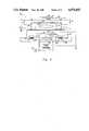
- FIG. 1is a diagrammatic view of a parallel plate reactor embodying the present invention
- FIG. 2is a view in elevation to an enlarged scale of the substrate supporting chuck shown in FIG. 1;
- FIG. 3is a view of another parallel plate reactor incorporating the present invention.
- FIG. 4is a view in section of a chuck that is similar to the chuck shown in FIG. 2;
- FIG. 5is a bottom plan view of the chuck of FIG. 4.
- a parallel plate reactoris generally designated 10 and includes an upper electrode 12 connected to a terminal of an RF generator 14 that may provide a 13.56 MHZ signal, for example, and have its other terminal grounded.
- the chuck 16 and an intermediate perforated electrode or rib 18are both at ground potential.
- the chuck 16is temperature insulated from the frame or housing 20 as by an annularly shaped insulator body 22.
- a fluorine containing gassuch as NF 3 , CF 4 or SF 6 , is available from supply 24 and directed through a gas opening in the housing cap which may be associated with the upper electrode 12.
- Chuck 16is provided with a temperature controller 26 which detects the chuck temperature and is effective to raise or, where desired, lower the chuck temperature.
- a temperature controller 26which detects the chuck temperature and is effective to raise or, where desired, lower the chuck temperature.
- An important feature of the present inventionis to maintain the temperature at a predetermined level which is different for different substrates and mask materials. While the temperature could be caused to vary according to a programmed schedule during the etching process, in the illustrated embodiment it is contemplated that the temperature will be held at a single level throughout the etching cycle of a particular substrate.
- the control signal from the temperature controller 26may cause heat to be added to the chuck 16 by electrical heaters dispersed throughout the block, by circulating a fluid in a channel in the block or by any other suitable heat adding device.
- the heat exchange fluidmay advantageously be a liquid such as water or a similar heat exchange liquid having a higher boiling point for operation at temperatures in excess of 100° C.
- the control signal from the temperature controller 26may cause heat to be removed from chuck 16. This is most easily accomplished by providing a liquid circulation path which may be in the form of a cavity or channel that is part of the chuck. A conventional heat exchanger may be used with the circulating liquid where desired.
- a cylindrical projection 30is shown to extend from the lower surface of chuck 16.
- the projection 30is provided with a number of equally spaced bores 32 for receiving electrical heaters.
- the power to the heatersis controlled by the temperature controller 26 shown in FIG. 1 thereby providing a temperature control loop and a stabilized temperature for chuck 16.
- Chuck 16is also shown to have a centrally disposed water cooling channel which is adapted to be supplied with tap water through an inlet 36 and an outlet 38.
- FIG. 3shows the preferred embodiment of the present invention which has been incorporated in a modified form of a parallel plate reactor of a type in commercial use that is the subject of a co-pending application of Gary Powell having Ser. No. 07/238,462 filed Aug. 30, 1988 and assigned to the assignee of the present invention. The disclosure of that application is hereby incorporated by reference.
- FIG. 3shows a cross sectional view of a parallel plate reactor, generally designated 40 which has an upper electrode portion 41, an upper RF chamber 42, a lower chamber 43, a lower electrode or chuck 44, and grid 45. As illustrated in FIG. 3, the plasma envelope 46 is generated between grid 45 and 41.
- Electrode 41consists of a cap 47 having a gas opening 48 therein. Cap 47 is mounted on a lid 49. Lid 49 also contains a gas opening 50 which coincides with opening 48 of cap 47. As is known in the art, lid 49 can contain vias for the circulation of water. The circulating water is used to cool reactor 40. Cap 47 acts as a cover for the water vias.
- Lid 49is disposed on a bottom disc 51 to form a gas mixing chamber therebetween.
- Disc 51contains a plurality of openings 54 through which reactant gas passes.
- the reactant gasis passed through openings 54 into upper chamber 42 where the plasma 46 is formed.
- the walls of chamber 42are provided by an insulator 55.
- the insulatoris made preferably of aluminum oxide (Al 22 O 3 ).
- Grid 45may be made of an electrically conductive perforated aluminum sheet that has any suitable shape.
- the grid 45is coupled to the inner surface of body 57. Disposed about grid 45 and defining the circumference of lower chamber 43 is a chamber body 57.
- the chamber body 57is mounted on a base plate 59 which has a central opening defined by vertical cylindrical walls 60.
- a base plate 59which has a central opening defined by vertical cylindrical walls 60.
- an annularly shaped insulator 61which is comprised for example, of aluminum oxide. It should be noted here that since grid 45 and lower electrode or chuck 44 are at the same electrical potential, the insulator 61 is solely for use as a heat insulator which is one of the changes that has been made to the device disclosed in the above-identified application.
- a substrate 64such as a semiconductor wafer, is disposed on the surface of the chuck 44 such that a surface of substrate 64 is facing lower chamber 43.
- the chuck or lower electrode 44 as incorporated in the device of FIG. 3has a cylindrical projection 66 which may have a central bore that serves as the cooling cavity and is adapted to receive a water cooling channel 68 that is indicated in FIG. 3.
- the projection 66which may have a nominal diameter of about 4", six equally spaced bores 70 (see FIG. 5) are provided which are adapted to receive the heater elements 72 as illustrated in FIG. 3.
- the temperature sensor 74may be connected to one of the leads from a power supply terminal 76 in order to regulate the amount of power supplied to each of the electrical heaters 72.
- the temperature sensormay comprise three equally spaced temperature sensing units 74a, 74b, 74c which are equally spaced and located to be between two adjacent heater elements in bores 70.
- each temperature sensing element 74controls the power supplied to the two immediately adjacent heating elements 72 that are in their respective bores 70.
- the number of temperature sensing elements 74a, 74b, 74cmay be one-half of the number of heater elements 72 with the heating elements that are on the opposite sides of a temperature sensing element being controlled by the intermediate temperature sensing element.
- the apparatus disclosedutilizes an electrically heated surface where the substrate temperature is regulated at temperatures in excess of 80° C. with accuracy and reproducibility.
- the controlembodies a closed loop heater arrangement that may optionally be coupled with a cooling loop to extend the effective lower limit of the control window.
Landscapes
- Engineering & Computer Science (AREA)
- Physics & Mathematics (AREA)
- Condensed Matter Physics & Semiconductors (AREA)
- General Physics & Mathematics (AREA)
- Manufacturing & Machinery (AREA)
- Computer Hardware Design (AREA)
- Microelectronics & Electronic Packaging (AREA)
- Power Engineering (AREA)
- Drying Of Semiconductors (AREA)
Abstract
Description
Claims (10)
Priority Applications (1)
| Application Number | Priority Date | Filing Date | Title |
|---|---|---|---|
| US07/494,173US4971653A (en) | 1990-03-14 | 1990-03-14 | Temperature controlled chuck for elevated temperature etch processing |
Applications Claiming Priority (1)
| Application Number | Priority Date | Filing Date | Title |
|---|---|---|---|
| US07/494,173US4971653A (en) | 1990-03-14 | 1990-03-14 | Temperature controlled chuck for elevated temperature etch processing |
Publications (1)
| Publication Number | Publication Date |
|---|---|
| US4971653Atrue US4971653A (en) | 1990-11-20 |
Family
ID=23963350
Family Applications (1)
| Application Number | Title | Priority Date | Filing Date |
|---|---|---|---|
| US07/494,173Expired - LifetimeUS4971653A (en) | 1990-03-14 | 1990-03-14 | Temperature controlled chuck for elevated temperature etch processing |
Country Status (1)
| Country | Link |
|---|---|
| US (1) | US4971653A (en) |
Cited By (56)
| Publication number | Priority date | Publication date | Assignee | Title |
|---|---|---|---|---|
| US5147497A (en)* | 1990-07-20 | 1992-09-15 | Tokyo Electron Limited | Plasma apparatus, and method and system for extracting electrical signal of member to which high-frequency wave is applied |
| US5171393A (en)* | 1991-07-29 | 1992-12-15 | Moffat William A | Wafer processing apparatus |
| US5192849A (en)* | 1990-08-10 | 1993-03-09 | Texas Instruments Incorporated | Multipurpose low-thermal-mass chuck for semiconductor processing equipment |
| US5200023A (en)* | 1991-08-30 | 1993-04-06 | International Business Machines Corp. | Infrared thermographic method and apparatus for etch process monitoring and control |
| US5209803A (en)* | 1988-08-30 | 1993-05-11 | Matrix Integrated Systems, Inc. | Parallel plate reactor and method of use |
| US5248371A (en)* | 1992-08-13 | 1993-09-28 | General Signal Corporation | Hollow-anode glow discharge apparatus |
| US5304250A (en)* | 1991-07-11 | 1994-04-19 | Sony Corporation | Plasma system comprising hollow mesh plate electrode |
| US5314573A (en)* | 1991-05-20 | 1994-05-24 | Tokyo Electron Limited | Dry etching polysilicon using a bromine-containing gas |
| US5344525A (en)* | 1991-01-29 | 1994-09-06 | Micron Technology, Inc. | Process for etching semiconductor devices |
| US5415753A (en)* | 1993-07-22 | 1995-05-16 | Materials Research Corporation | Stationary aperture plate for reactive sputter deposition |
| US5595241A (en)* | 1994-10-07 | 1997-01-21 | Sony Corporation | Wafer heating chuck with dual zone backplane heating and segmented clamping member |
| US5609720A (en)* | 1995-09-29 | 1997-03-11 | Lam Research Corporation | Thermal control of semiconductor wafer during reactive ion etching |
| WO1997019303A1 (en)* | 1995-11-17 | 1997-05-29 | Cvc Products, Inc. | Temperature controlled chuck for vacuum processing |
| US5637189A (en)* | 1996-06-25 | 1997-06-10 | Xerox Corporation | Dry etch process control using electrically biased stop junctions |
| US5637237A (en)* | 1994-03-08 | 1997-06-10 | International Business Machines Corporation | Method for hot wall reactive ion etching using a dielectric or metallic liner with temperature control to achieve process stability |
| US5647945A (en)* | 1993-08-25 | 1997-07-15 | Tokyo Electron Limited | Vacuum processing apparatus |
| US5711851A (en)* | 1996-07-12 | 1998-01-27 | Micron Technology, Inc. | Process for improving the performance of a temperature-sensitive etch process |
| US5783100A (en)* | 1994-03-16 | 1998-07-21 | Micron Display Technology, Inc. | Method of high density plasma etching for semiconductor manufacture |
| US5865938A (en)* | 1996-06-25 | 1999-02-02 | Xerox Corporation | Wafer chuck for inducing an electrical bias across wafer heterojunctions |
| US5892207A (en)* | 1995-12-01 | 1999-04-06 | Teisan Kabushiki Kaisha | Heating and cooling apparatus for reaction chamber |
| US5916411A (en)* | 1995-06-21 | 1999-06-29 | Sony Corporation | Dry etching system |
| US5936829A (en)* | 1997-01-02 | 1999-08-10 | Cvc Products, Inc. | Thermally conductive chuck for vacuum processor |
| US6014082A (en)* | 1997-10-03 | 2000-01-11 | Sony Corporation | Temperature monitoring and calibration system for control of a heated CVD chuck |
| US6063710A (en)* | 1996-02-26 | 2000-05-16 | Sony Corporation | Method and apparatus for dry etching with temperature control |
| US6132805A (en)* | 1998-10-20 | 2000-10-17 | Cvc Products, Inc. | Shutter for thin-film processing equipment |
| US6138745A (en)* | 1997-09-26 | 2000-10-31 | Cvc Products, Inc. | Two-stage sealing system for thermally conductive chuck |
| US6156667A (en)* | 1999-12-31 | 2000-12-05 | Litmas, Inc. | Methods and apparatus for plasma processing |
| US6302057B1 (en) | 1998-09-15 | 2001-10-16 | Tokyo Electron Limited | Apparatus and method for electrically isolating an electrode in a PECVD process chamber |
| US20020005252A1 (en)* | 1995-03-16 | 2002-01-17 | Toshio Masuda | Plasma etching apparatus and plasma etching method |
| US6367410B1 (en) | 1996-12-16 | 2002-04-09 | Applied Materials, Inc. | Closed-loop dome thermal control apparatus for a semiconductor wafer processing system |
| US6373679B1 (en) | 1999-07-02 | 2002-04-16 | Cypress Semiconductor Corp. | Electrostatic or mechanical chuck assembly conferring improved temperature uniformity onto workpieces held thereby, workpiece processing technology and/or apparatus containing the same, and method(s) for holding and/or processing a workpiece with the same |
| US6406545B2 (en) | 1999-07-27 | 2002-06-18 | Kabushiki Kaisha Toshiba | Semiconductor workpiece processing apparatus and method |
| KR20020062074A (en)* | 2001-01-19 | 2002-07-25 | 주식회사 템네스트 | Temperature controlling system for the surface of an electrostatic chuck using heaters |
| US6451217B1 (en)* | 1998-06-09 | 2002-09-17 | Speedfam-Ipec Co., Ltd. | Wafer etching method |
| US20020129769A1 (en)* | 2001-03-19 | 2002-09-19 | Apex Co. Ltd. | Chemical vapor deposition apparatus |
| US6508885B1 (en) | 1997-11-25 | 2003-01-21 | Cvc Products, Inc. | Edge sealing structure for substrate in low-pressure processing environment |
| US20030016727A1 (en)* | 2001-06-29 | 2003-01-23 | Tokyo Electron Limited | Method of and apparatus for measuring and controlling substrate holder temperature using ultrasonic tomography |
| US20030029610A1 (en)* | 1997-01-02 | 2003-02-13 | Cvc Products, Inc. | Thermally conductive chuck for vacuum processor |
| WO2003046970A1 (en)* | 2001-11-21 | 2003-06-05 | The Regents Of The University Of California | Low temperature compatible wide-pressure-range plasma flow device |
| US20030154921A1 (en)* | 2002-02-19 | 2003-08-21 | Nobuo Matsuki | Apparatus and method for forming low dielectric constant film |
| US20030186545A1 (en)* | 2002-04-02 | 2003-10-02 | Lam Research Corporation, A Delaware Corporation | Variable temperature processes for tunable electrostatic chuck |
| US20030183252A1 (en)* | 2001-03-26 | 2003-10-02 | Timperio Onofio L. | Plasma etcher with heated ash chamber base |
| US20030196760A1 (en)* | 2002-04-19 | 2003-10-23 | Nordson Corporation | Plasma treatment system |
| US6705394B1 (en) | 1999-10-29 | 2004-03-16 | Cvc Products, Inc. | Rapid cycle chuck for low-pressure processing |
| US20040129282A1 (en)* | 2001-05-04 | 2004-07-08 | Carlos Munoz | Apparatus and method for delaminating parcels of tobacco |
| US20040187787A1 (en)* | 2003-03-31 | 2004-09-30 | Dawson Keith E. | Substrate support having temperature controlled substrate support surface |
| US20050016455A1 (en)* | 2002-03-29 | 2005-01-27 | Cheon-Soo Cho | Surface treatment system and method |
| US20050026436A1 (en)* | 2000-12-21 | 2005-02-03 | Hogan Timothy J. | Method for improving ash rate uniformity in photoresist ashing process equipment |
| US20050045276A1 (en)* | 2001-05-22 | 2005-03-03 | Patel Satyadev R. | Method for making a micromechanical device by removing a sacrificial layer with multiple sequential etchants |
| US6905333B2 (en) | 2002-09-10 | 2005-06-14 | Axcelis Technologies, Inc. | Method of heating a substrate in a variable temperature process using a fixed temperature chuck |
| WO2006077390A1 (en)* | 2005-01-18 | 2006-07-27 | Point 35 Microstructures Limited | Improved method and apparatus for monitoring a microstructure etching process |
| US20090310645A1 (en)* | 2008-06-16 | 2009-12-17 | Hitachi-High Technologies Corporation | Sample temperature control method |
| CN102648512A (en)* | 2009-11-18 | 2012-08-22 | 圆益Ips股份有限公司 | Shower head assembly and thin film deposition apparatus comprising same |
| US20140076234A1 (en)* | 2004-02-26 | 2014-03-20 | Applied Materials, Inc. | Multi chamber processing system |
| US20180230597A1 (en)* | 2017-02-14 | 2018-08-16 | Applied Materials, Inc. | Method and apparatus of remote plasmas flowable cvd chamber |
| US11485123B2 (en)* | 2020-07-07 | 2022-11-01 | Samsung Display Co., Ltd. | Lamination apparatus |
Citations (2)
| Publication number | Priority date | Publication date | Assignee | Title |
|---|---|---|---|---|
| US4565601A (en)* | 1983-09-12 | 1986-01-21 | Hitachi, Ltd. | Method and apparatus for controlling sample temperature |
| US4886571A (en)* | 1988-02-24 | 1989-12-12 | Hitachi, Ltd. | Surface treatment and apparatus therefor |
- 1990
- 1990-03-14USUS07/494,173patent/US4971653A/ennot_activeExpired - Lifetime
Patent Citations (2)
| Publication number | Priority date | Publication date | Assignee | Title |
|---|---|---|---|---|
| US4565601A (en)* | 1983-09-12 | 1986-01-21 | Hitachi, Ltd. | Method and apparatus for controlling sample temperature |
| US4886571A (en)* | 1988-02-24 | 1989-12-12 | Hitachi, Ltd. | Surface treatment and apparatus therefor |
Cited By (88)
| Publication number | Priority date | Publication date | Assignee | Title |
|---|---|---|---|---|
| US5209803A (en)* | 1988-08-30 | 1993-05-11 | Matrix Integrated Systems, Inc. | Parallel plate reactor and method of use |
| US5147497A (en)* | 1990-07-20 | 1992-09-15 | Tokyo Electron Limited | Plasma apparatus, and method and system for extracting electrical signal of member to which high-frequency wave is applied |
| US5192849A (en)* | 1990-08-10 | 1993-03-09 | Texas Instruments Incorporated | Multipurpose low-thermal-mass chuck for semiconductor processing equipment |
| US5344525A (en)* | 1991-01-29 | 1994-09-06 | Micron Technology, Inc. | Process for etching semiconductor devices |
| US5314573A (en)* | 1991-05-20 | 1994-05-24 | Tokyo Electron Limited | Dry etching polysilicon using a bromine-containing gas |
| US5304250A (en)* | 1991-07-11 | 1994-04-19 | Sony Corporation | Plasma system comprising hollow mesh plate electrode |
| US5171393A (en)* | 1991-07-29 | 1992-12-15 | Moffat William A | Wafer processing apparatus |
| US5200023A (en)* | 1991-08-30 | 1993-04-06 | International Business Machines Corp. | Infrared thermographic method and apparatus for etch process monitoring and control |
| US5248371A (en)* | 1992-08-13 | 1993-09-28 | General Signal Corporation | Hollow-anode glow discharge apparatus |
| WO1994005035A1 (en)* | 1992-08-13 | 1994-03-03 | Lam Research Corporation | Hollow-anode glow discharge apparatus |
| US5415753A (en)* | 1993-07-22 | 1995-05-16 | Materials Research Corporation | Stationary aperture plate for reactive sputter deposition |
| US5647945A (en)* | 1993-08-25 | 1997-07-15 | Tokyo Electron Limited | Vacuum processing apparatus |
| US5637237A (en)* | 1994-03-08 | 1997-06-10 | International Business Machines Corporation | Method for hot wall reactive ion etching using a dielectric or metallic liner with temperature control to achieve process stability |
| US5798016A (en)* | 1994-03-08 | 1998-08-25 | International Business Machines Corporation | Apparatus for hot wall reactive ion etching using a dielectric or metallic liner with temperature control to achieve process stability |
| US5783100A (en)* | 1994-03-16 | 1998-07-21 | Micron Display Technology, Inc. | Method of high density plasma etching for semiconductor manufacture |
| US5595241A (en)* | 1994-10-07 | 1997-01-21 | Sony Corporation | Wafer heating chuck with dual zone backplane heating and segmented clamping member |
| US20020005252A1 (en)* | 1995-03-16 | 2002-01-17 | Toshio Masuda | Plasma etching apparatus and plasma etching method |
| US5916411A (en)* | 1995-06-21 | 1999-06-29 | Sony Corporation | Dry etching system |
| US5609720A (en)* | 1995-09-29 | 1997-03-11 | Lam Research Corporation | Thermal control of semiconductor wafer during reactive ion etching |
| US5950723A (en)* | 1995-11-17 | 1999-09-14 | Cvc Products, Inc. | Method of regulating substrate temperature in a low pressure environment |
| GB2323152A (en)* | 1995-11-17 | 1998-09-16 | Cvc Products Inc | Temperature controlled chuck for vacuum processing |
| US5775416A (en)* | 1995-11-17 | 1998-07-07 | Cvc Products, Inc. | Temperature controlled chuck for vacuum processing |
| GB2323152B (en)* | 1995-11-17 | 2000-03-22 | Cvc Products Inc | Temperature controlled chuck for vacuum processing |
| WO1997019303A1 (en)* | 1995-11-17 | 1997-05-29 | Cvc Products, Inc. | Temperature controlled chuck for vacuum processing |
| US5892207A (en)* | 1995-12-01 | 1999-04-06 | Teisan Kabushiki Kaisha | Heating and cooling apparatus for reaction chamber |
| US6063710A (en)* | 1996-02-26 | 2000-05-16 | Sony Corporation | Method and apparatus for dry etching with temperature control |
| US5865938A (en)* | 1996-06-25 | 1999-02-02 | Xerox Corporation | Wafer chuck for inducing an electrical bias across wafer heterojunctions |
| US5637189A (en)* | 1996-06-25 | 1997-06-10 | Xerox Corporation | Dry etch process control using electrically biased stop junctions |
| US6221205B1 (en) | 1996-07-12 | 2001-04-24 | Micron Technology, Inc. | Apparatus for improving the performance of a temperature-sensitive etch |
| US6056850A (en)* | 1996-07-12 | 2000-05-02 | Micron Technology, Inc. | Apparatus for improving the performance of a temperature-sensitive etch process |
| US5711851A (en)* | 1996-07-12 | 1998-01-27 | Micron Technology, Inc. | Process for improving the performance of a temperature-sensitive etch process |
| US6413875B1 (en) | 1996-07-12 | 2002-07-02 | Micron Technology, Inc. | Process and apparatus for improving the performance of a temperature-sensitive etch process |
| US6367410B1 (en) | 1996-12-16 | 2002-04-09 | Applied Materials, Inc. | Closed-loop dome thermal control apparatus for a semiconductor wafer processing system |
| US20030029610A1 (en)* | 1997-01-02 | 2003-02-13 | Cvc Products, Inc. | Thermally conductive chuck for vacuum processor |
| US6907924B2 (en) | 1997-01-02 | 2005-06-21 | Veeco Rochester Inc. | Thermally conductive chuck for vacuum processor |
| US5936829A (en)* | 1997-01-02 | 1999-08-10 | Cvc Products, Inc. | Thermally conductive chuck for vacuum processor |
| US6138745A (en)* | 1997-09-26 | 2000-10-31 | Cvc Products, Inc. | Two-stage sealing system for thermally conductive chuck |
| US6378600B1 (en) | 1997-09-26 | 2002-04-30 | Cvc Products, Inc. | Thermally conductive chuck with thermally separated sealing structures |
| US6124793A (en)* | 1997-10-03 | 2000-09-26 | Sony Corporation | Temperature monitoring and calibration system for control of a heated CVD chuck |
| US6014082A (en)* | 1997-10-03 | 2000-01-11 | Sony Corporation | Temperature monitoring and calibration system for control of a heated CVD chuck |
| US6508885B1 (en) | 1997-11-25 | 2003-01-21 | Cvc Products, Inc. | Edge sealing structure for substrate in low-pressure processing environment |
| US6451217B1 (en)* | 1998-06-09 | 2002-09-17 | Speedfam-Ipec Co., Ltd. | Wafer etching method |
| US6302057B1 (en) | 1998-09-15 | 2001-10-16 | Tokyo Electron Limited | Apparatus and method for electrically isolating an electrode in a PECVD process chamber |
| US6132805A (en)* | 1998-10-20 | 2000-10-17 | Cvc Products, Inc. | Shutter for thin-film processing equipment |
| US6373679B1 (en) | 1999-07-02 | 2002-04-16 | Cypress Semiconductor Corp. | Electrostatic or mechanical chuck assembly conferring improved temperature uniformity onto workpieces held thereby, workpiece processing technology and/or apparatus containing the same, and method(s) for holding and/or processing a workpiece with the same |
| US6406545B2 (en) | 1999-07-27 | 2002-06-18 | Kabushiki Kaisha Toshiba | Semiconductor workpiece processing apparatus and method |
| US6705394B1 (en) | 1999-10-29 | 2004-03-16 | Cvc Products, Inc. | Rapid cycle chuck for low-pressure processing |
| US6156667A (en)* | 1999-12-31 | 2000-12-05 | Litmas, Inc. | Methods and apparatus for plasma processing |
| US20050026436A1 (en)* | 2000-12-21 | 2005-02-03 | Hogan Timothy J. | Method for improving ash rate uniformity in photoresist ashing process equipment |
| KR20020062074A (en)* | 2001-01-19 | 2002-07-25 | 주식회사 템네스트 | Temperature controlling system for the surface of an electrostatic chuck using heaters |
| US7410676B2 (en) | 2001-03-19 | 2008-08-12 | Ips Ltd. | Chemical vapor deposition method |
| US20050217582A1 (en)* | 2001-03-19 | 2005-10-06 | Apex Co., Ltd. | Chemical vapor deposition method |
| US20020129769A1 (en)* | 2001-03-19 | 2002-09-19 | Apex Co. Ltd. | Chemical vapor deposition apparatus |
| US6886491B2 (en)* | 2001-03-19 | 2005-05-03 | Apex Co. Ltd. | Plasma chemical vapor deposition apparatus |
| US20030183252A1 (en)* | 2001-03-26 | 2003-10-02 | Timperio Onofio L. | Plasma etcher with heated ash chamber base |
| US7810506B2 (en) | 2001-05-04 | 2010-10-12 | Philip Morris Usa Inc. | Apparatus and method for delaminating parcels of tobacco |
| US20040129282A1 (en)* | 2001-05-04 | 2004-07-08 | Carlos Munoz | Apparatus and method for delaminating parcels of tobacco |
| US20050045276A1 (en)* | 2001-05-22 | 2005-03-03 | Patel Satyadev R. | Method for making a micromechanical device by removing a sacrificial layer with multiple sequential etchants |
| US20030016727A1 (en)* | 2001-06-29 | 2003-01-23 | Tokyo Electron Limited | Method of and apparatus for measuring and controlling substrate holder temperature using ultrasonic tomography |
| US20050089077A1 (en)* | 2001-06-29 | 2005-04-28 | Tokyo Electron Limited | Method of and apparatus for measuring and controlling substrate holder temperature using ultrasonic tomography |
| WO2003046970A1 (en)* | 2001-11-21 | 2003-06-05 | The Regents Of The University Of California | Low temperature compatible wide-pressure-range plasma flow device |
| US6830007B2 (en)* | 2002-02-19 | 2004-12-14 | Asm Japan K.K. | Apparatus and method for forming low dielectric constant film |
| US20030154921A1 (en)* | 2002-02-19 | 2003-08-21 | Nobuo Matsuki | Apparatus and method for forming low dielectric constant film |
| US20050016455A1 (en)* | 2002-03-29 | 2005-01-27 | Cheon-Soo Cho | Surface treatment system and method |
| US7677199B2 (en)* | 2002-03-29 | 2010-03-16 | Lg Electronics Inc. | Surface treatment system and method |
| US20030186545A1 (en)* | 2002-04-02 | 2003-10-02 | Lam Research Corporation, A Delaware Corporation | Variable temperature processes for tunable electrostatic chuck |
| US6921724B2 (en)* | 2002-04-02 | 2005-07-26 | Lam Research Corporation | Variable temperature processes for tunable electrostatic chuck |
| CN1323427C (en)* | 2002-04-02 | 2007-06-27 | 蓝姆研究公司 | Variable temperature processing for adjustable electrostatic chucks |
| US20050269031A1 (en)* | 2002-04-19 | 2005-12-08 | Nordson Corporation | Plasma treatment system |
| US7013834B2 (en)* | 2002-04-19 | 2006-03-21 | Nordson Corporation | Plasma treatment system |
| US20030196760A1 (en)* | 2002-04-19 | 2003-10-23 | Nordson Corporation | Plasma treatment system |
| US8613827B2 (en) | 2002-04-19 | 2013-12-24 | Nordson Corporation | Plasma treatment system |
| US6905333B2 (en) | 2002-09-10 | 2005-06-14 | Axcelis Technologies, Inc. | Method of heating a substrate in a variable temperature process using a fixed temperature chuck |
| US20050166845A1 (en)* | 2002-09-10 | 2005-08-04 | Gerald Cox | Method of heating a substrate in a variable temperature process using a fixed temperature chuck |
| US7485190B2 (en) | 2002-09-10 | 2009-02-03 | Axcelis Technologies, Inc. | Apparatus for heating a substrate in a variable temperature process using a fixed temperature chuck |
| US20040187787A1 (en)* | 2003-03-31 | 2004-09-30 | Dawson Keith E. | Substrate support having temperature controlled substrate support surface |
| CN100565787C (en)* | 2003-03-31 | 2009-12-02 | 兰姆研究公司 | Base sheet rack with surface of controlled temperature |
| WO2004093167A3 (en)* | 2003-03-31 | 2005-06-09 | Lam Res Corp | Substrate support having temperature controlled surface |
| US20140076234A1 (en)* | 2004-02-26 | 2014-03-20 | Applied Materials, Inc. | Multi chamber processing system |
| WO2006077390A1 (en)* | 2005-01-18 | 2006-07-27 | Point 35 Microstructures Limited | Improved method and apparatus for monitoring a microstructure etching process |
| US7672750B2 (en) | 2005-01-18 | 2010-03-02 | Point 35 Microstructures Ltd. | Method and apparatus for monitoring a microstructure etching process |
| US20080147229A1 (en)* | 2005-01-18 | 2008-06-19 | Point 35 Microstructures Limited | Method And Apparatus For Monitoring A Microstructure Etching Process |
| US8093529B2 (en)* | 2008-06-16 | 2012-01-10 | Hitachi High-Technologies Corporation | Control method of a temperature of a sample |
| US20090310645A1 (en)* | 2008-06-16 | 2009-12-17 | Hitachi-High Technologies Corporation | Sample temperature control method |
| CN102648512A (en)* | 2009-11-18 | 2012-08-22 | 圆益Ips股份有限公司 | Shower head assembly and thin film deposition apparatus comprising same |
| CN102648512B (en)* | 2009-11-18 | 2015-04-29 | 圆益Ips股份有限公司 | Shower head assembly and thin film deposition apparatus comprising same |
| US20180230597A1 (en)* | 2017-02-14 | 2018-08-16 | Applied Materials, Inc. | Method and apparatus of remote plasmas flowable cvd chamber |
| US11485123B2 (en)* | 2020-07-07 | 2022-11-01 | Samsung Display Co., Ltd. | Lamination apparatus |
Similar Documents
| Publication | Publication Date | Title |
|---|---|---|
| US4971653A (en) | Temperature controlled chuck for elevated temperature etch processing | |
| CN101110381B (en) | Substrate processing with rapid temperature gradient control | |
| TWI517761B (en) | Shielded lid heater assembly | |
| US10257887B2 (en) | Substrate support assembly | |
| US4963713A (en) | Cooling of a plasma electrode system for an etching apparatus | |
| US6303526B1 (en) | Temperature controlled spin chuck | |
| US4148705A (en) | Gas plasma reactor and process | |
| US5892207A (en) | Heating and cooling apparatus for reaction chamber | |
| KR100395846B1 (en) | In-situ wafer temperature controller for single wafer tool | |
| US4209357A (en) | Plasma reactor apparatus | |
| US6890403B2 (en) | Apparatus and process for controlling the temperature of a substrate in a plasma reactor | |
| JP3242166B2 (en) | Etching equipment | |
| JP5906249B2 (en) | Plasma processing equipment | |
| KR100246994B1 (en) | Plasma processing apparatus | |
| KR20100108323A (en) | Workpiece support with fluid zones for temperature control | |
| WO2014052301A1 (en) | Controlling temperature in substrate processing systems | |
| KR101590566B1 (en) | Plasma apparatus for vapor phase etching and cleaning | |
| KR102623545B1 (en) | Apparatus for manufacturing semiconductor device | |
| KR101569956B1 (en) | High throughput processing system for chemical treatment and thermal treatment and method of operating | |
| US4474621A (en) | Method for low temperature ashing in a plasma | |
| KR100567493B1 (en) | Apparatus for forming coating film and apparatus for curing the coating film | |
| JP2022143369A (en) | Plasma processing apparatus | |
| JPH09320799A (en) | Plasma processing apparatus and plasma processing method | |
| JPH0487321A (en) | Holding device of object to be treated in vacuum treatment apparatus | |
| KR20240022756A (en) | ESC temperature control unit and substrate treating apparatus including the same |
Legal Events
| Date | Code | Title | Description |
|---|---|---|---|
| AS | Assignment | Owner name:MATRIX INTEGRATED SYSTEMS, CALIFORNIA Free format text:ASSIGNMENT OF ASSIGNORS INTEREST.;ASSIGNOR:DRAGE, DAVID J.;REEL/FRAME:005441/0664 Effective date:19900301 | |
| FEPP | Fee payment procedure | Free format text:PAYOR NUMBER ASSIGNED (ORIGINAL EVENT CODE: ASPN); ENTITY STATUS OF PATENT OWNER: SMALL ENTITY | |
| FEPP | Fee payment procedure | Free format text:PAT HOLDER CLAIMS SMALL ENTITY STATUS - SMALL BUSINESS (ORIGINAL EVENT CODE: SM02); ENTITY STATUS OF PATENT OWNER: SMALL ENTITY | |
| FPAY | Fee payment | Year of fee payment:4 | |
| AS | Assignment | Owner name:SILICON VALLEY BANK, CALIFORNIA Free format text:SECURITY INTEREST;ASSIGNOR:MATRIX INTEGRATED SYSTEMS, INC.;REEL/FRAME:007095/0532 Effective date:19931001 | |
| FPAY | Fee payment | Year of fee payment:8 | |
| AS | Assignment | Owner name:SILICON VALLEY BANK COMMERICAL FINANCE DIVISON, CA Free format text:SECURITY INTEREST;ASSIGNOR:MATRIX INTEGRATED SYSTEMS, INC;REEL/FRAME:010007/0974 Effective date:19970415 | |
| REMI | Maintenance fee reminder mailed | ||
| REIN | Reinstatement after maintenance fee payment confirmed | ||
| FEPP | Fee payment procedure | Free format text:PETITION RELATED TO MAINTENANCE FEES GRANTED (ORIGINAL EVENT CODE: PMFG); ENTITY STATUS OF PATENT OWNER: SMALL ENTITY | |
| FP | Lapsed due to failure to pay maintenance fee | Effective date:20021120 | |
| PRDP | Patent reinstated due to the acceptance of a late maintenance fee | Effective date:20030128 | |
| STCF | Information on status: patent grant | Free format text:PATENTED CASE | |
| AS | Assignment | Owner name:MATRIX INTEGRATED SYSTEMS, INC., CALIFORNIA Free format text:RELEASE;ASSIGNOR:SILICON VALLEY BANK;REEL/FRAME:014373/0686 Effective date:20030804 | |
| REFU | Refund | Free format text:REFUND - PAYMENT OF MAINTENANCE FEE, 12TH YR, SMALL ENTITY (ORIGINAL EVENT CODE: R2553); ENTITY STATUS OF PATENT OWNER: SMALL ENTITY | |
| AS | Assignment | Owner name:EXCELIS TECHNOLOGIES, INC., MASSACHUSETTS Free format text:ASSIGNMENT OF ASSIGNORS INTEREST;ASSIGNOR:MATRIX INTEGRATED SYSTEMS, INC.;REEL/FRAME:014885/0260 Effective date:20031130 | |
| FEPP | Fee payment procedure | Free format text:PAYER NUMBER DE-ASSIGNED (ORIGINAL EVENT CODE: RMPN); ENTITY STATUS OF PATENT OWNER: SMALL ENTITY Free format text:PAYOR NUMBER ASSIGNED (ORIGINAL EVENT CODE: ASPN); ENTITY STATUS OF PATENT OWNER: SMALL ENTITY | |
| AS | Assignment | Owner name:SILICON VALLEY BANK, CALIFORNIA Free format text:SECURITY AGREEMENT;ASSIGNOR:AXCELIS TECHNOLOGIES, INC.;REEL/FRAME:020986/0143 Effective date:20080423 Owner name:SILICON VALLEY BANK,CALIFORNIA Free format text:SECURITY AGREEMENT;ASSIGNOR:AXCELIS TECHNOLOGIES, INC.;REEL/FRAME:020986/0143 Effective date:20080423 |