US4968970A - Method of and system for power line carrier communications - Google Patents
Method of and system for power line carrier communicationsDownload PDFInfo
- Publication number
- US4968970A US4968970AUS07/343,202US34320289AUS4968970AUS 4968970 AUS4968970 AUS 4968970AUS 34320289 AUS34320289 AUS 34320289AUS 4968970 AUS4968970 AUS 4968970A
- Authority
- US
- United States
- Prior art keywords
- logical
- signal
- encoded
- signals
- output
- Prior art date
- Legal status (The legal status is an assumption and is not a legal conclusion. Google has not performed a legal analysis and makes no representation as to the accuracy of the status listed.)
- Expired - Lifetime
Links
Images


Classifications
- H—ELECTRICITY
- H04—ELECTRIC COMMUNICATION TECHNIQUE
- H04B—TRANSMISSION
- H04B3/00—Line transmission systems
- H04B3/54—Systems for transmission via power distribution lines
- H—ELECTRICITY
- H04—ELECTRIC COMMUNICATION TECHNIQUE
- H04B—TRANSMISSION
- H04B1/00—Details of transmission systems, not covered by a single one of groups H04B3/00 - H04B13/00; Details of transmission systems not characterised by the medium used for transmission
- H04B1/69—Spread spectrum techniques
- H04B1/713—Spread spectrum techniques using frequency hopping
- H—ELECTRICITY
- H02—GENERATION; CONVERSION OR DISTRIBUTION OF ELECTRIC POWER
- H02J—CIRCUIT ARRANGEMENTS OR SYSTEMS FOR SUPPLYING OR DISTRIBUTING ELECTRIC POWER; SYSTEMS FOR STORING ELECTRIC ENERGY
- H02J13/00—Circuit arrangements for providing remote indication of network conditions, e.g. an instantaneous record of the open or closed condition of each circuitbreaker in the network; Circuit arrangements for providing remote control of switching means in a power distribution network, e.g. switching in and out of current consumers by using a pulse code signal carried by the network
- H02J13/00006—Circuit arrangements for providing remote indication of network conditions, e.g. an instantaneous record of the open or closed condition of each circuitbreaker in the network; Circuit arrangements for providing remote control of switching means in a power distribution network, e.g. switching in and out of current consumers by using a pulse code signal carried by the network characterised by information or instructions transport means between the monitoring, controlling or managing units and monitored, controlled or operated power network element or electrical equipment
- H02J13/00007—Circuit arrangements for providing remote indication of network conditions, e.g. an instantaneous record of the open or closed condition of each circuitbreaker in the network; Circuit arrangements for providing remote control of switching means in a power distribution network, e.g. switching in and out of current consumers by using a pulse code signal carried by the network characterised by information or instructions transport means between the monitoring, controlling or managing units and monitored, controlled or operated power network element or electrical equipment using the power network as support for the transmission
- H02J13/00009—Circuit arrangements for providing remote indication of network conditions, e.g. an instantaneous record of the open or closed condition of each circuitbreaker in the network; Circuit arrangements for providing remote control of switching means in a power distribution network, e.g. switching in and out of current consumers by using a pulse code signal carried by the network characterised by information or instructions transport means between the monitoring, controlling or managing units and monitored, controlled or operated power network element or electrical equipment using the power network as support for the transmission using pulsed signals
- H—ELECTRICITY
- H04—ELECTRIC COMMUNICATION TECHNIQUE
- H04B—TRANSMISSION
- H04B3/00—Line transmission systems
- H04B3/54—Systems for transmission via power distribution lines
- H04B3/542—Systems for transmission via power distribution lines the information being in digital form
- H—ELECTRICITY
- H04—ELECTRIC COMMUNICATION TECHNIQUE
- H04B—TRANSMISSION
- H04B2203/00—Indexing scheme relating to line transmission systems
- H04B2203/54—Aspects of powerline communications not already covered by H04B3/54 and its subgroups
- H04B2203/5404—Methods of transmitting or receiving signals via power distribution lines
- H04B2203/5416—Methods of transmitting or receiving signals via power distribution lines by adding signals to the wave form of the power source
- H—ELECTRICITY
- H04—ELECTRIC COMMUNICATION TECHNIQUE
- H04B—TRANSMISSION
- H04B2203/00—Indexing scheme relating to line transmission systems
- H04B2203/54—Aspects of powerline communications not already covered by H04B3/54 and its subgroups
- H04B2203/5429—Applications for powerline communications
- H04B2203/5433—Remote metering
- H—ELECTRICITY
- H04—ELECTRIC COMMUNICATION TECHNIQUE
- H04B—TRANSMISSION
- H04B2203/00—Indexing scheme relating to line transmission systems
- H04B2203/54—Aspects of powerline communications not already covered by H04B3/54 and its subgroups
- H04B2203/5462—Systems for power line communications
- H04B2203/5483—Systems for power line communications using coupling circuits
- H—ELECTRICITY
- H04—ELECTRIC COMMUNICATION TECHNIQUE
- H04B—TRANSMISSION
- H04B2203/00—Indexing scheme relating to line transmission systems
- H04B2203/54—Aspects of powerline communications not already covered by H04B3/54 and its subgroups
- H04B2203/5462—Systems for power line communications
- H04B2203/5491—Systems for power line communications using filtering and bypassing
- Y—GENERAL TAGGING OF NEW TECHNOLOGICAL DEVELOPMENTS; GENERAL TAGGING OF CROSS-SECTIONAL TECHNOLOGIES SPANNING OVER SEVERAL SECTIONS OF THE IPC; TECHNICAL SUBJECTS COVERED BY FORMER USPC CROSS-REFERENCE ART COLLECTIONS [XRACs] AND DIGESTS
- Y02—TECHNOLOGIES OR APPLICATIONS FOR MITIGATION OR ADAPTATION AGAINST CLIMATE CHANGE
- Y02E—REDUCTION OF GREENHOUSE GAS [GHG] EMISSIONS, RELATED TO ENERGY GENERATION, TRANSMISSION OR DISTRIBUTION
- Y02E60/00—Enabling technologies; Technologies with a potential or indirect contribution to GHG emissions mitigation
- Y—GENERAL TAGGING OF NEW TECHNOLOGICAL DEVELOPMENTS; GENERAL TAGGING OF CROSS-SECTIONAL TECHNOLOGIES SPANNING OVER SEVERAL SECTIONS OF THE IPC; TECHNICAL SUBJECTS COVERED BY FORMER USPC CROSS-REFERENCE ART COLLECTIONS [XRACs] AND DIGESTS
- Y04—INFORMATION OR COMMUNICATION TECHNOLOGIES HAVING AN IMPACT ON OTHER TECHNOLOGY AREAS
- Y04S—SYSTEMS INTEGRATING TECHNOLOGIES RELATED TO POWER NETWORK OPERATION, COMMUNICATION OR INFORMATION TECHNOLOGIES FOR IMPROVING THE ELECTRICAL POWER GENERATION, TRANSMISSION, DISTRIBUTION, MANAGEMENT OR USAGE, i.e. SMART GRIDS
- Y04S40/00—Systems for electrical power generation, transmission, distribution or end-user application management characterised by the use of communication or information technologies, or communication or information technology specific aspects supporting them
- Y04S40/12—Systems for electrical power generation, transmission, distribution or end-user application management characterised by the use of communication or information technologies, or communication or information technology specific aspects supporting them characterised by data transport means between the monitoring, controlling or managing units and monitored, controlled or operated electrical equipment
- Y04S40/121—Systems for electrical power generation, transmission, distribution or end-user application management characterised by the use of communication or information technologies, or communication or information technology specific aspects supporting them characterised by data transport means between the monitoring, controlling or managing units and monitored, controlled or operated electrical equipment using the power network as support for the transmission
Definitions
- This inventionrelates generally to power line carrier communications, and more particularly to a power line carrier communications method and system using frequency hopping type spread spectrum signal modulation and demodulation.
- remote watthour metersare polled by a central computer which maintains customer electricity consumption records for billing.
- a central computerwhich maintains customer electricity consumption records for billing.
- power linesare electrically noisy so that it is difficult to establish a reliable communications link between the meters and the central computer using a reasonably small amount of signal power.
- the noise spectrum of the power lineschanges with time of the day and season of the year depending on operation of electrical equipment connect, or located in proximity, to the power lines.
- power line network characteristicshave variations in attenuation as a function of frequency, with pronounced dips in transmission of some frequencies that vary among networks.
- Noise injected on the linesincludes fixed frequency noise resulting, for example, from the switching of inductive loads.
- Other noisearises at harmonics of the frequency of the network, and there is gaussian background noise as well as fluctuating signals caused by televisions and the like operating on the power lines.
- one object of the inventionis to provide a method of and system for establishing reliable communications between local and remote data reporting equipment.
- Another object of the inventionis to provide reliable power line communications method and apparatus suitable for centralized meter reading.
- each information element to be sentis encoded by a sequence of several different predetermined coding frequencies, wherein one sequence represents a logical-one bit and another represents a logical-zero bit.
- the two sequences of frequenciesare within two different bands that are frequency spaced apart from each other.
- signals of equal ranki.e.
- the sequencesare demodulated at a receiver coupled to the power line by correlation with locally generated signals that produce, with a substantially constant frequency shift, the particular frequency combinations and the value of the information element being determined as a function of the correlation output.
- the Galula et al. systemis relatively complex, requires constraint in selection of frequencies forming the sequences and under certain circumstances may interpret received bits incorrectly. Complexity is a result of heterodyne signal demodulation that requires intermediate frequency conversion and amplification prior to correlation.
- the selection of frequenciesis limited to frequencies within two different bands. Signal components which occupy one of the band are applied to one of the demodulators while the other components which occupy the other band are applied to the other demodulator, and as mentioned hereinabove the frequencies are not arbitrarily selectable since at least frequencies in corresponding ranks within the two bands must not be the same.
- a correlation decisionis made in Galula et al.
- the decisionmay identify a logical-one or logical-zero bit incorrectly as noise.
- a further object of the inventionis to provide a power line carrier communication method and system having improved immunity to line noise.
- Another object of the inventionis to provide more accurate bit detection in a frequency hopping type power line communication system.
- a further objectis to provide a frequency hopping type power line communication system that has simplified demodulation circuitry and wherein demodulation can be carried out in part by software.
- Still another objectis to provide a frequency hopping type power line communication system that has its frequencies distributed in a common band and minimum frequency selection constraints.
- a system for wideband transmission of data on an electricity distribution networkcomprising at least one transmitter for generating encoded signals corresponding respectively to logical-one bits and logical-zero bits.
- Each encoded signal corresponding to a logical-one bitconsists of a first predetermined, unrelated sequence of frequencies and each encoded signal corresponding to a logical-zero bit consists of a second, different predetermined and unrelated sequence of frequencies.
- the output of the transmitteris coupled on the electricity distribution network and at least one receiver coupled to the network receives from the transmitter input encoded signals.
- the receiverincludes a first demodulator in at least a first frequency channel for converting the logical-one bit signals into corresponding first dc signals, a second demodulator in at least a second frequency channel for converting the logical-zero signals into corresponding second dc signals, and offset compensation circuitry for compensating the receiver for an offset voltage developed as a result of component offsets therein.
- a comparatoris provided for comparing output signals from the first and second channels indicating a logical-one or logical-zero bit.
- the receiverincludes a homodyne demodulator system comprising a first demodulator with first and second channels for demodulating logical-one bit signals.
- a first local signal generatorprovides a first reference signal that is a replica of the encoded logical-one bit signal, a first multiplier for forming a product of the input encoded signal and the first reference signal, a first filter coupled to an output of the first multiplier for passing substantially only a first dc component therefrom, and a first squaring circuit for squaring the first dc component.
- a second local signal generatorprovides a second reference signal that is, in quadrature, a replica of the said encoded logical-one bit signal, a second multiplier for forming a product of the input encoded signal and the second reference signal, a second filter coupled to an output of the second multiplier for passing substantially only a second dc component therefrom, and a second squaring circuit for squaring the second dc component.
- a first summeris provided for summing outputs of the first and second squaring circuits, and a first integrator accumulates from the first summer first output signals corresponding to the first sequence of frequencies.
- the receiverfurther includes a second demodulator having third and fourth channels for demodulating the logical-zero bit signals.
- a third local signal generatorprovides a third reference signal that is a replica of the encoded logical-zero bit signal, a third multiplier for forming a product of the input encoded signal and the third reference signal, a third filter coupled to an output of the third multiplier for passing substantially only a third dc component therefrom, and a third squaring circuit for squaring the third dc component.
- a fourth local signal generatorprovides a fourth reference signal that is, in quadrature, a replica of the encoded logical-zero bit signal, a fourth multiplier for forming a product of the input encoded signal and the fourth reference signal, a fourth filter coupled to an output of the fourth multiplier means for passing substantially only a fourth dc component therefrom, and a fourth squaring circuit for squaring the fourth dc component.
- a second summeris provided for summing outputs of the third and fourth squaring circuits and a second integrator accumulates from the second summer second output signals corresponding to the second sequence of frequencies. The integration periods of the first and second integrators is equal to the number of sequences forming a bit.
- a comparatoris provided for comparing output signals from the first and second integrators for indicating a logical-one or logical-zero bit.
- the comparatorthus establishes a bit decision based upon all "hops" of the sequence forming a bit rather than upon a comparison of the energy content individually of successive hops in logical-one and logical-zero bits.
- offset compensation circuitrycompensates the receiver for any error voltage developed as a result of receiver component offsets.
- the offset compensation circuitrypreferably includes a circuit for shunting an input of the receiver to provide a "zero input" thereto whereby the output voltage developed by the receiver is attributed only to offset voltage produced therein. This offset is then calculated by a micro-processor, and the offset compensation is carried out by software.
- the receiver and transmitter of the systemboth are synchronized to electricity on the electricity distribution network.
- synchronization circuitry in the systemincludes a zero crossing detector synchronized to zero crossings of electricity on the electricity distribution network for generating line synchronization pulses.
- a phase locked loop responsive to the line synchronization pulsescontrols generation of encoded signals by the transmitter.
- a limiter circuitfor limiting the input signal applied to the receiver.
- a transformercouples the encoded signals from the electricity distribution network to the receiver, and a band pass filter between the transformer and the receiver limits the frequency range of the input signals.
- the transmitterincludes a frequency synthesizer for generating respectively the logical-one and logical-zero encoded signals.
- front end demodulationis carried out in hardware, and the remainder of the demodulation is implemented in software.
- wide band data transmission on an electricity distribution networkis carried out by generating encoded signals corresponding respectively to logical-one bits and logical-zero bits, wherein each encoded signal corresponds to a logical-one bit consisting of a first predetermined, unrelated sequence of frequencies and each encoded signal corresponds to a logical-zero bit consisting of a second, different predetermined, unrelated sequence of frequencies.
- the encoded signalsare coupled on the electricity distribution network and input encoded signals on the electricity distribution network are received.
- Receivingincludes establishing first and second frequency channels for demodulating the logical-one bit signals and third and fourth channels for demodulating the logical-zero bit signals.
- a first reference signalthat is a replica of the encoded logical-one bit signal and a first product signal that is a product of the input encoded signal and the first reference signal.
- the first product signalis filtered for passing substantially only a first dc component thereof which is squared to obtain a first output signal.
- Provided in the second channelare a second local signal that is, in quadrature, a replica of the encoded logical-one bit signal and a second product signal that is a product of the input encoded signal and the second reference signal.
- the second reference signalis filtered for passing substantially only a second dc component thereof which is squared to obtain a second output signal.
- a third reference signalthat is a replica of the encoded logical-zero bit signal and a third product of the input encoded signal and the third reference signal
- the third reference signalis filtered for passing substantially only a third dc component thereof which is squared to obtain a third output signal.
- a fourth reference signalthat is, in quadrature, a replica of the encoded logical-zero bit signal and a fourth product of the input encoded signal and the fourth reference signal.
- the fourth reference signalis filtered for passing substantially only a fourth dc component thereof which is squared to obtain a fourth output signal.
- the first and second output signalsare summed to obtain a first summed output signal corresponding to the first sequence of frequencies, and similarly, the third and fourth output signals are summed to obtain a second summed output signal corresponding to the second sequence of frequencies.
- the first summed signalis integrated to obtain a first integrated output signal, and the second summed signal is integrated to obtain a second integrated output signal.
- the first and second integrated output signalsare compared to each other for indicating a logical-one or logical-zero bit.
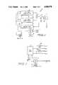
- FIG. 1is symbolic drawing of a multiple tenant building containing a large number of individual units each having an energy meter on the power lines distributed therein, and a building control unit for polling the energy meters to accumulate individualized energy consumption,. data for billing or other purpose.
- FIG. 2(a)is an example of coding combinations of logical-one and logical-zero bits using two different frequency sequences
- FIG. 2(b)is another example of coding frequency combinations of logical-one and logical-zero bits using the same sequence in quadrature to represent the two bits.
- FIG. 3is a simplified block diagram of a transmitter provided in accordance with one aspect of the invention for generating the coding frequency combinations of FIGS. 2(a) and 2(b) within the system shown in FIG. 1..
- FIG. 4is a block diagram of a receiver provided in accordance with another aspect of the invention, for carrying out homodyne, non-coherent, demodulation of the encoded carrier signals injected on the power lines by the transmitter of FIG. 3.
- FIG. 5is a diagram of the circuit for generating the four reference signals shown in FIG. 4, and for synchronizing the receiver and transmitter to zero crossings on the power lines.
- FIG. 6is a circuit diagram of offset compensation for compensating offset voltages produced in the demodulation channels of the receiver shown in FIG. 4.
- FIG. 7is a circuit diagram of the receiver having software implemented demodulation functions.
- the environment to which the invention may be applied but is not limitedincludes, as shown, an apartment building B that may have a large number of individual apartments therein, each being provided with electricity by a commercial utility over a common set of power lines PL.
- electricity meters EMDistributed on the power lines PL, and located within the individual units are electricity meters EM which monitor and accumulate electricity consumption in each unit.
- the electricity meters EMare polled by a building control unit BCU centrally located in the building B and consisting of or containing a local computer which may be a "personal computer" connected to a power line modem PLM for coupling a modulated carrier signal between the BCU and the power line PL.
- Each electricity meter EM as wellincludes a modem and line interface to enable bidirectional communications between the EM. and the BCU to take place over the power lines directly if the two are on a common power transformer or through another EM or a PLM used as a bridge if the two are on different transformers.
- each of the electricity meters EMthere is a transmitter of a type identified by 10 in FIG. 3, coupled to the low voltage power lines PL and within the PLM, a receiver of a type identified by 30 in FIG. 4 is also coupled to the lines.
- each meter EMcontains a receiver 30, and the PLM also preferably contains a transmitter 10, to enable carrying out of communication routing, as described in the copending application.
- Each transmitter 10, shown in FIG. 3,comprises a register 12 where information to be transmitted, such as the reading of a meter (not shown) is stored in the form of a digital word of several bits.
- a microprocessor 14receives each bit for transmission and converts each bit into addresses of a memory 16 defining memory locations that store a predetermined sequence of coding frequencies to be developed by a frequency synthesizer section 18.
- a first predetermined frequency combinationis used for coding a logical-one bit and a second predetermined frequency combination is used for coding a logical-zero bit.
- the signal produced by synthesizer section 18is of the form of a train of frequency bursts, the frequency of which varies stepwise periodically during transmission of the bit and is synchronized to the electricity on the power line by a synchronization unit 20.
- FIG. 2(a)An example of successive frequency values used for logical-one and logical-zero bit coding is shown in FIG. 2(a).
- 1 and logical-zero bitsare coded as sequences of four successive frequencies, or "hops" (sometimes also called “chips").
- hopssometimes also called “chips”
- a logical-one bitis coded into the sequence F11, F12, F13 and F14; these four hops are synchronized to a half cycle of electricity on power lines PL, as shown on the abscissa of the graph.
- a logical-zero bit, synchronized to the electricity on line PLconsists of the sequence F01, F02, F03 and F04.
- the number of hops forming each bitis optional; a larger number of hops per bit of further may reduce error rate but increases the complexity and processing speed requirements of the transmitter and receiver circuitry.
- the choice of frequencies forming the hopsalso is arbitrary, although it is preferable to maintain a high degree of difference in sequences between the coded logical-one and logical-zero bits to improve synchronization between the transmitter and receiver. Accordingly, it is advantageous to code the bits such that corresponding hops, that is, frequencies within a common rank of logical-one and logical-zero bits, are different from each other. It is furthermore advantageous to separate the frequencies by a multiple of 120*n Hertz from each other where n is the number of hop per bit. In the examples shown in FIG. 2(a), the hops fall within a frequency band bounded by 50 and 150 kilohertz; the baud rate is 120 bps.
- FIG. 2(b)Another example of successive frequency values used for bit coding, shown in FIG. 2(b) provides a total of four different frequencies F11, F12, F13 and F14 comprising the sequence for a logical-one bit, and F01, F02, F03 and F04 which is the same frequency sequence, in quadrature, forms the coded logical-zero bits.
- the frequency of the first hop in a logical-one bit sequence (F11)is equal to the frequency of the third hop (F03) of the logical-zero bit sequence
- the frequency of the second hop in a logical-one bit sequence (F12)is equal to the frequency of the fourth hop (F04) of the logical-zero bit sequence.
- the hopsagain are in the band bounded by 50 and 150 kilohertz; transmission is at 120 bps.
- FIGS. 2(a) and 2(b)An important advantage of the coding shown in FIGS. 2(a) and 2(b) is that the coded logical-one and logical-zero bits are integrated in a common band, that is, the frequencies of the two sequences overlap with each other. This provides greater versatility than that in the Galula et al. patent.
- the code sequences representing logical-one and logical-zero bitsare prestored in memory 16, and can be altered by programming. Addresses stored in memory 16, corresponding to the two sequences, are supplied to address inputs of a conventional frequency synthesizer 18. Frequency synthesizer 18 generates coded logical-one bits and coded logical-zero bits. The microprocessor 14 controls the code which needs to be sent to the frequency synthsizer according to what is in memory 18 and to the logical bit to send on the line. Output of the synthesizer is amplified in amplifier 24 and then injected on power lines PL through line interface transformer LI.
- the frequency synthesizer 18generates a discrete frequency signal in response to an address, e.g., an eight bit word, applied to its address input. Accordingly, to generate a coded logical-one or logical-zero bit, the frequency synthesizer will receive a sequence of words corresponding to the hops forming that bit.
- the frequency synthesizer 18can be software or firmware if preferred.
- a watchdog timer 26monitors the output of the frequency synthesizer unit 18. Each time the unit 18 generates a sequence, the watchdog timer 26 measures the time duration of the sequence. If the measured duration exceeds that of a predetermined sequence duration, operation of the synthesizer is presumed to be defective, and the watchdog timer 26 resets the synthesizer. Transmission so that transmission of a carrier by the transmitter 10 is thereby terminated until another transmission cycle takes place.
- receiver 30 in each meter EMmonitors the power lines PL at line interface transformer LI.
- the signal detected by the transformeris applied to a bandpass filter 32 that minimizes the amount of noise detected on the power lines by limiting the frequency of line signals to be processed in the receiver.
- the bandpass filter 32preferably attenuates network low frequencies, principally the network frequency and its harmonics, and limits the upper band beyond the highest coding frequency used, e.g., approximately 100-150 kHz.
- the output of filter 32is amplified by an amplifier 34 and conditioned by a limiter 36 to eliminate signals detected on the power lines that extend beyond the normal operating range of the receiver.
- the output of limiter 36is a conditioned replica of the modulated carrier injected on power lines PL by the transmitter 10, and has the form
- Node AAforms an input of a non-coherent, homodyne demodulator circuit in accordance with the invention, for accurately detecting logical-one and logical-zero bits received by the receiver 30.
- the demodulatoridentified generally by 38, carries out demodulation in four frequency channels 38(a), 38(b), 38(c) and 38(d).
- the input channel at AAis multiplied by a reference signal developed by a local generator, shown in FIG. 5.
- a first multiplier 40(a) in channel 38(a)multiplies the input signal at node AA by first locally generated reference signal cos(w11t) that corresponds to the frequencies forming a logical-one sequence. This sequence of frequencies is generated by frequency synthesizer 51(a) in FIG. 5, and is resident at the receiver.
- the output of multiplier 40(a) at line Al of the first channel 38(a)therefore is
- the second multiplier 40(b) in channel 38(b)obtains the product of the input signal at node AA and a second reference signal sin(wllt) developed by frequency synthesizer 51(a); the second reference signal thus is a replica of, and is in quadrature with, the first reference signal.
- the third and fourth reference signals applied to multipliers 40(c) and 40(d)correspond to a logical-zero sequence of frequencies.
- the third and fourth reference signals in channels 38(c) and 38(d)thus respectively are cos(w01t) and sin(w01t). both generated by the frequency synthesizer 51(b) in FIG. 5.
- the fourth reference signal in channel 38(d)is a replica of, and is in quadrature with, the third reference signal in third channel 38(c).
- the four reference signals generated by frequency synthesizers 51(a) and 51(b) (FIG. 5)are controlled by a microprocessor 52, and the synthesizers are synchronized to electricity on the power lines by a zero crossover detector 54 for synchronizing a phase locked loop 56. Since zero crossover detectors 54 and phase lock loops 56 are well known to persons skilled in the art, no details are provided herein.
- Quadrature reference signalsare derived from signals on other channels by phase shifters 58(a) and 58(b) in the manner shown.
- Equations (2) to (5)can be expanded respectively as follows:
- a sideband of the input signal at AAis impressed either on lines B1 and B2 of channels 38(a) and 38(b) or on lines B3 and B4 of channels 38(c) and 38(d). depending upon whether an encoded logical-one bit signal or an encoded logical-zero bit signal is received.
- the signals on lines B1 and B2are in quadrature with each other, and similarly, the signals on lines B3 and B4 are in quadrature.
- the outputs of low pass filters 42(a)-(d)are applied to respective squaring circuits 44(a)-(d), so that the signals on lines C1, C2, C3 and C4 are, respectively, (a/2) 2 cos 2 (phi), (a/2) 2 sin 2 (phi), 0 and 0.
- the outputs of squaring circuits 44(a)-(d)in turn are applied to first and second summers 46(a) and 46(b). Specifically, the outputs of the squaring circuits 44(a) and 44(b) in the first and second channels 38(a), 38(b) are added together in 46(a), so that the signal on line D1,2 is as shown in equation (14)
- the signal on either output line D1,2 or output line D3,4, depending upon whether a logical-one bit or logical-zero bit is received by the receiver 30,is a2.
- integrator 48(b)if a logical-one bit signal is received, a dc signal having a magnitude a/4 applied on line D1,2 is integrated in integrator circuit 48b; the signal on the other output line D3,4, attributable to noise, is applied to integrator 48(b).
- the integration period of integrators 48(a) and 48(b)is equal to the number of hops per bit, e.g., four in the examples shown in FIGS. 2(a) and (b).
- the outputs of the integrators on output lines E1,2 and E3,4are supplied to the inputs of a comparator 50 which applies a signal, on which indicates whether a logical-one bit or logical-zero bit signal has been received on output line F.
- the comparator 50accordingly determines whether the signals accumulated on channels 38(a) and 38(b) during a bit sequence are greater or less than the signals on channels 38(c) and 38(d). If the magnitude is greater, the bit received is deemed to be, e.g., a logical-one and if the magnitude is less the received bit in this example is considered to be a logical-zero bit.
- a bit decisionis not made by comparing energy content in the logical-one bit and logical-zero bit channel pairs instead, the magnitudes of signals on output lines D1,2 and D3,4 are summed through all hops of a bit sequence and then a bit decision is made.
- a bit decisionis made once for each four hop sequence. This technique eliminates the bit determination ambiguities inherent in the Gulala et al patent, supra.
- the circuit of FIG. 4compares the sum of four samples on each output line E1,2 and E3,4. The difference is determined in comparator 50, and if the difference is greater than that attributable to noise, a logical-one bit or logical-zero bit determination is made.
- the level of noisewhich forms a calibration reference for the receiver 30, is determined on a regular basis which can be advantageously chosen equal to one hour.
- Noise on lines E1,2 and E3,4are in the form of dc signals that are imparted as offset voltage as a result of voltage imbalances within components of the receiver 30.
- Offset detection and correction circuitryshown in FIG. 6, for reducing the magnitude of this offset voltage comprises a first controlled switch 60 in shunt with the input of the receiver 30. At the beginning of a calibration cycle, the switch 60 is closed, connecting the input of the receiver 30 to ground whereby any dc output level from the receiver is attributable only to noise.
- This dc levelis stored in a microprocessor 62, thereafter, during the operation mode of the receiver, microprocessor 62 subtracts the stored offset from the signal output of receiver 30. Offset compensation thus is carried out as each bit is received.
- receiver 30,shown in FIG. 7, has a demodulation section that is at least partially software or firmware implemented.
- microprocessor 62is programmed to carry out the functions at least of squaring circuits 44, summers 46, integrators 48 and comparators 50. Programming of a microprocessor to carry out the functions of those circuits, as described supra, is well known to persons skilled in the art.
Landscapes
- Engineering & Computer Science (AREA)
- Power Engineering (AREA)
- Computer Networks & Wireless Communication (AREA)
- Signal Processing (AREA)
- Cable Transmission Systems, Equalization Of Radio And Reduction Of Echo (AREA)
- Digital Transmission Methods That Use Modulated Carrier Waves (AREA)
- Transmitters (AREA)
- Small-Scale Networks (AREA)
- Compression, Expansion, Code Conversion, And Decoders (AREA)
- Detection And Prevention Of Errors In Transmission (AREA)
- Transmission Systems Not Characterized By The Medium Used For Transmission (AREA)
- Remote Monitoring And Control Of Power-Distribution Networks (AREA)
- Treating Waste Gases (AREA)
- Heat Treatment Of Sheet Steel (AREA)
- Gas Separation By Absorption (AREA)
Abstract
Description
a . cos(w11 t+phi) (1)
a . cos (w11t+phi) . cos(w11t) (3)
a . cos (w11t+phi) . sin (w11t) (3)
a . cos (w11t+phi) . cos (w01t) (4)
a . cos (w11t+phi) . sin (w01t) (5)
______________________________________ a/2.( cos(2w11t+phi)t + cos(phi)) (6) a/2.( sin(2w11t+phi)t + sin(phi)) (7) a/2.( cos[(w11+w01)t+phi] + cos[(w11-w01)t+phi]) (8) a/2.( sin[(w11+w01)t+phi] + sin[(w11-w01)t+phi]) (9) ______________________________________
______________________________________ a/2.(cos(phi)) (10) a/2.(sin(phi)) (11) 0 (12) 0 (13) ______________________________________
______________________________________ a/4 (cos.sup.2 (phi) + sin.sup.2 (phi) ) = a/4 (14) since cos.sup.2 (phi) + sin.sup.2 (phi) = 1 (15) ______________________________________
0 (16)
Claims (27)
Priority Applications (9)
| Application Number | Priority Date | Filing Date | Title |
|---|---|---|---|
| US07/343,202US4968970A (en) | 1989-04-26 | 1989-04-26 | Method of and system for power line carrier communications |
| KR1019900005931AKR900017312A (en) | 1989-04-26 | 1990-04-25 | Broadband Transmission System and Transmission Method of Data in Distribution Network |
| DE69021120TDE69021120T2 (en) | 1989-04-26 | 1990-04-25 | Method and device for transmissions with carrier frequency over the power lines. |
| EP90401103AEP0395494B1 (en) | 1989-04-26 | 1990-04-25 | Method of and system for power line carrier communications |
| FI902069AFI902069A7 (en) | 1989-04-26 | 1990-04-25 | Method and system for obtaining carrier wave information on power lines |
| AT90401103TATE125651T1 (en) | 1989-04-26 | 1990-04-25 | METHOD AND DEVICE FOR CARRIER FREQUENCY TRANSMISSIONS OVER POWER LINES. |
| CA002015414ACA2015414C (en) | 1989-04-26 | 1990-04-25 | Method of and system for power line carrier communications |
| BR909001953ABR9001953A (en) | 1989-04-26 | 1990-04-26 | APPLIANCE AND WIDE-BAND DATA TRANSMISSION PROCESS IN AN ELECTRICITY DISTRIBUTION NETWORK |
| JP2111603AJPH0362743A (en) | 1989-04-26 | 1990-04-26 | Method and apparatus of power line carrier communication |
Applications Claiming Priority (1)
| Application Number | Priority Date | Filing Date | Title |
|---|---|---|---|
| US07/343,202US4968970A (en) | 1989-04-26 | 1989-04-26 | Method of and system for power line carrier communications |
Publications (1)
| Publication Number | Publication Date |
|---|---|
| US4968970Atrue US4968970A (en) | 1990-11-06 |
Family
ID=23345113
Family Applications (1)
| Application Number | Title | Priority Date | Filing Date |
|---|---|---|---|
| US07/343,202Expired - LifetimeUS4968970A (en) | 1989-04-26 | 1989-04-26 | Method of and system for power line carrier communications |
Country Status (9)
| Country | Link |
|---|---|
| US (1) | US4968970A (en) |
| EP (1) | EP0395494B1 (en) |
| JP (1) | JPH0362743A (en) |
| KR (1) | KR900017312A (en) |
| AT (1) | ATE125651T1 (en) |
| BR (1) | BR9001953A (en) |
| CA (1) | CA2015414C (en) |
| DE (1) | DE69021120T2 (en) |
| FI (1) | FI902069A7 (en) |
Cited By (50)
| Publication number | Priority date | Publication date | Assignee | Title |
|---|---|---|---|---|
| WO1993001660A1 (en)* | 1991-07-12 | 1993-01-21 | Abb Power T&D Company Inc. | Power distribution line communication system for reducing effects of signal cancellation |
| US5319634A (en)* | 1991-10-07 | 1994-06-07 | Phoenix Corporation | Multiple access telephone extension systems and methods |
| US5452344A (en)* | 1992-05-29 | 1995-09-19 | Datran Systems Corporation | Communication over power lines |
| US5517172A (en)* | 1994-09-19 | 1996-05-14 | Chiu; Manfred F. | Method and apparatus for powering and signaling over a single wire pair |
| US5530737A (en)* | 1993-03-22 | 1996-06-25 | Phonex Corporation | Secure access telephone extension system and method |
| US5818821A (en) | 1994-12-30 | 1998-10-06 | Intelogis, Inc. | Universal lan power line carrier repeater system and method |
| US5911119A (en)* | 1993-03-22 | 1999-06-08 | Phonex Corporation | Secure cordless telephone extension system and method |
| US5912633A (en)* | 1994-08-18 | 1999-06-15 | Remote Metering Systems Limited | Mains signalling systems |
| US5970127A (en) | 1997-10-16 | 1999-10-19 | Phonex Corporation | Caller identification system for wireless phone jacks and wireless modem jacks |
| US6055435A (en) | 1997-10-16 | 2000-04-25 | Phonex Corporation | Wireless telephone connection surge suppressor |
| US6107912A (en) | 1997-12-08 | 2000-08-22 | Phonex Corporation | Wireless modem jack |
| US20010002210A1 (en)* | 1997-02-14 | 2001-05-31 | Petite Thomas D. | Multi-function general purpose transceiver |
| US6243571B1 (en) | 1998-09-21 | 2001-06-05 | Phonex Corporation | Method and system for distribution of wireless signals for increased wireless coverage using power lines |
| US6246868B1 (en) | 1998-08-14 | 2001-06-12 | Phonex Corporation | Conversion and distribution of incoming wireless telephone signals using the power line |
| WO2001082491A1 (en)* | 2000-04-19 | 2001-11-01 | Phonex Broadband Corporation | Method and system for power line null detection and automatic frequency and gain control |
| US20030078029A1 (en)* | 2001-10-24 | 2003-04-24 | Statsignal Systems, Inc. | System and method for transmitting an emergency message over an integrated wireless network |
| US20030093484A1 (en)* | 2001-10-30 | 2003-05-15 | Petite Thomas D. | System and method for tansmitting pollution information over an integrated wireless network |
| WO2003071708A1 (en)* | 2002-02-21 | 2003-08-28 | Rutherford J G | A communications system utilising electricity cabling |
| US20040053639A1 (en)* | 1997-02-14 | 2004-03-18 | Petite Thomas D. | System and method for communicating with a remote communication unit via the public switched telephone network (PSTN) |
| US20050169401A1 (en)* | 2004-02-02 | 2005-08-04 | Satius, Inc. | Frequency modulated OFDM over various communication media |
| US20050190055A1 (en)* | 1998-06-22 | 2005-09-01 | Statsignal Ipc, Llc | Smoke detection methods, devices, and systems |
| US20050195768A1 (en)* | 2004-03-03 | 2005-09-08 | Petite Thomas D. | Method for communicating in dual-modes |
| US20050243867A1 (en)* | 1998-06-22 | 2005-11-03 | Statsignal Ipc, Llc | Systems and methods for monitoring and controlling remote devices |
| US7053767B2 (en) | 1998-06-22 | 2006-05-30 | Statsignal Systems, Inc. | System and method for monitoring and controlling remote devices |
| US7103511B2 (en) | 1998-10-14 | 2006-09-05 | Statsignal Ipc, Llc | Wireless communication networks for providing remote monitoring of devices |
| US20060223364A1 (en)* | 2003-10-03 | 2006-10-05 | Asoka Usa Corporation | Method and system for virtual powerline local area networks |
| US7137550B1 (en) | 1997-02-14 | 2006-11-21 | Statsignal Ipc, Llc | Transmitter for accessing automated financial transaction machines |
| RU2288507C1 (en)* | 2005-11-16 | 2006-11-27 | Общество с ограниченной ответственностью "АЛЬТОНИКА" (ООО "АЛЬТОНИКА") | Method for generation of resulting series of synchronization impulses during transfer of information by means of code messages along alternating-current electric network |
| RU2288506C1 (en)* | 2005-11-14 | 2006-11-27 | Общество с ограниченной ответственностью "АЛЬТОНИКА" (ООО "АЛЬТОНИКА") | Method for generation of resulting series of synchronizing impulses during transfer of information via three-phased alternating-current electric network |
| US20060269002A1 (en)* | 2004-08-12 | 2006-11-30 | Martin Feldtkeller | Method for data transmission via a data transmission path with inductive transformers, and a data transmission apparatus |
| US7209840B2 (en) | 2000-08-09 | 2007-04-24 | Hunt Technologies, Llc | Systems and methods for providing remote monitoring of electricity consumption for an electric meter |
| US7263073B2 (en) | 1999-03-18 | 2007-08-28 | Statsignal Ipc, Llc | Systems and methods for enabling a mobile user to notify an automated monitoring system of an emergency situation |
| US7346463B2 (en) | 2001-08-09 | 2008-03-18 | Hunt Technologies, Llc | System for controlling electrically-powered devices in an electrical network |
| US7424031B2 (en) | 1998-07-28 | 2008-09-09 | Serconet, Ltd. | Local area network of serial intelligent cells |
| US20080247447A1 (en)* | 2004-09-08 | 2008-10-09 | Satius, Inc. | Apparatus and method for transmitting digital data over various communication media |
| US20090137219A1 (en)* | 2005-05-20 | 2009-05-28 | Andrew Williams | Near Field RF Communications |
| US7650425B2 (en) | 1999-03-18 | 2010-01-19 | Sipco, Llc | System and method for controlling communication between a host computer and communication devices associated with remote devices in an automated monitoring system |
| US7656904B2 (en) | 2003-03-13 | 2010-02-02 | Mosaid Technologies Incorporated | Telephone system having multiple distinct sources and accessories therefor |
| US20100074304A1 (en)* | 2008-09-22 | 2010-03-25 | Silver Spring Networks, Inc. | Power Line Communication Using Frequency Hopping |
| RU2405264C2 (en)* | 2009-02-11 | 2010-11-27 | Федеральное государственное унитарное предприятие "Ленинградский отраслевой научно-исследовательский институт связи" | Method for synchronisation of linear transport network built as based on system of synchronous digital hierarchy transfer system |
| US7876767B2 (en) | 2000-04-19 | 2011-01-25 | Mosaid Technologies Incorporated | Network combining wired and non-wired segments |
| US8000314B2 (en) | 1996-12-06 | 2011-08-16 | Ipco, Llc | Wireless network system and method for providing same |
| US8031650B2 (en) | 2004-03-03 | 2011-10-04 | Sipco, Llc | System and method for monitoring remote devices with a dual-mode wireless communication protocol |
| US8064412B2 (en) | 1998-06-22 | 2011-11-22 | Sipco, Llc | Systems and methods for monitoring conditions |
| US20120093198A1 (en)* | 2010-10-08 | 2012-04-19 | Texas Instruments Incorporated | Building, Transmitting, and Receiving Frame Structures in Power Line Communications |
| US8410931B2 (en) | 1998-06-22 | 2013-04-02 | Sipco, Llc | Mobile inventory unit monitoring systems and methods |
| US8489063B2 (en) | 2001-10-24 | 2013-07-16 | Sipco, Llc | Systems and methods for providing emergency messages to a mobile device |
| US8787246B2 (en) | 2009-02-03 | 2014-07-22 | Ipco, Llc | Systems and methods for facilitating wireless network communication, satellite-based wireless network systems, and aircraft-based wireless network systems, and related methods |
| US9439126B2 (en) | 2005-01-25 | 2016-09-06 | Sipco, Llc | Wireless network protocol system and methods |
| US12433671B2 (en) | 2016-11-28 | 2025-10-07 | Dfine, Inc. | Tumor ablation devices and related methods |
Families Citing this family (3)
| Publication number | Priority date | Publication date | Assignee | Title |
|---|---|---|---|---|
| GB9419807D0 (en)* | 1994-09-30 | 1994-11-16 | Remote Metering Systems Ltd | Mains signalling systems |
| JP2001345742A (en)* | 2000-05-31 | 2001-12-14 | Smk Corp | SS transmission system |
| GB2536907A (en) | 2015-03-30 | 2016-10-05 | Lighting And Illumination Tech Experience Ltd | Controlling power to a load with signals along a power line |
Citations (3)
| Publication number | Priority date | Publication date | Assignee | Title |
|---|---|---|---|---|
| US4641322A (en)* | 1983-10-18 | 1987-02-03 | Nec Corporation | System for carrying out spread spectrum communication through an electric power line |
| US4760586A (en)* | 1984-12-29 | 1988-07-26 | Kyocera Corporation | Spread spectrum communication system |
| US4763103A (en)* | 1985-02-14 | 1988-08-09 | Enertec | Process and method for wide band transmission, particularly for data transmission over an electricity distribution network |
Family Cites Families (1)
| Publication number | Priority date | Publication date | Assignee | Title |
|---|---|---|---|---|
| US4300125A (en)* | 1979-06-01 | 1981-11-10 | Loshing Clement T | System for monitoring, transmitting and conditioning of information gathered at selected locations |
- 1989
- 1989-04-26USUS07/343,202patent/US4968970A/ennot_activeExpired - Lifetime
- 1990
- 1990-04-25FIFI902069Apatent/FI902069A7/ennot_activeApplication Discontinuation
- 1990-04-25CACA002015414Apatent/CA2015414C/ennot_activeExpired - Lifetime
- 1990-04-25ATAT90401103Tpatent/ATE125651T1/ennot_activeIP Right Cessation
- 1990-04-25DEDE69021120Tpatent/DE69021120T2/ennot_activeExpired - Fee Related
- 1990-04-25EPEP90401103Apatent/EP0395494B1/ennot_activeExpired - Lifetime
- 1990-04-25KRKR1019900005931Apatent/KR900017312A/ennot_activeWithdrawn
- 1990-04-26JPJP2111603Apatent/JPH0362743A/enactivePending
- 1990-04-26BRBR909001953Apatent/BR9001953A/ennot_activeApplication Discontinuation
Patent Citations (3)
| Publication number | Priority date | Publication date | Assignee | Title |
|---|---|---|---|---|
| US4641322A (en)* | 1983-10-18 | 1987-02-03 | Nec Corporation | System for carrying out spread spectrum communication through an electric power line |
| US4760586A (en)* | 1984-12-29 | 1988-07-26 | Kyocera Corporation | Spread spectrum communication system |
| US4763103A (en)* | 1985-02-14 | 1988-08-09 | Enertec | Process and method for wide band transmission, particularly for data transmission over an electricity distribution network |
Cited By (107)
| Publication number | Priority date | Publication date | Assignee | Title |
|---|---|---|---|---|
| US5185591A (en)* | 1991-07-12 | 1993-02-09 | Abb Power T&D Co., Inc. | Power distribution line communication system for and method of reducing effects of signal cancellation |
| AU648171B2 (en)* | 1991-07-12 | 1994-04-14 | Abb Power T & D Company Inc. | Power distribution line communication system for and method of reducing effects of signal cancellation |
| WO1993001660A1 (en)* | 1991-07-12 | 1993-01-21 | Abb Power T&D Company Inc. | Power distribution line communication system for reducing effects of signal cancellation |
| US5319634A (en)* | 1991-10-07 | 1994-06-07 | Phoenix Corporation | Multiple access telephone extension systems and methods |
| US5452344A (en)* | 1992-05-29 | 1995-09-19 | Datran Systems Corporation | Communication over power lines |
| US5852785A (en) | 1993-03-22 | 1998-12-22 | Bartholomew; David B. | Secure access telephone extension system and method in a cordless telephone system |
| US5530737A (en)* | 1993-03-22 | 1996-06-25 | Phonex Corporation | Secure access telephone extension system and method |
| US5911119A (en)* | 1993-03-22 | 1999-06-08 | Phonex Corporation | Secure cordless telephone extension system and method |
| US5912633A (en)* | 1994-08-18 | 1999-06-15 | Remote Metering Systems Limited | Mains signalling systems |
| US5517172A (en)* | 1994-09-19 | 1996-05-14 | Chiu; Manfred F. | Method and apparatus for powering and signaling over a single wire pair |
| US5818821A (en) | 1994-12-30 | 1998-10-06 | Intelogis, Inc. | Universal lan power line carrier repeater system and method |
| US8000314B2 (en) | 1996-12-06 | 2011-08-16 | Ipco, Llc | Wireless network system and method for providing same |
| US8233471B2 (en) | 1996-12-06 | 2012-07-31 | Ipco, Llc | Wireless network system and method for providing same |
| US8625496B2 (en) | 1996-12-06 | 2014-01-07 | Ipco, Llc | Wireless network system and method for providing same |
| US8982856B2 (en) | 1996-12-06 | 2015-03-17 | Ipco, Llc | Systems and methods for facilitating wireless network communication, satellite-based wireless network systems, and aircraft-based wireless network systems, and related methods |
| US20040053639A1 (en)* | 1997-02-14 | 2004-03-18 | Petite Thomas D. | System and method for communicating with a remote communication unit via the public switched telephone network (PSTN) |
| US20010002210A1 (en)* | 1997-02-14 | 2001-05-31 | Petite Thomas D. | Multi-function general purpose transceiver |
| US7397907B2 (en) | 1997-02-14 | 2008-07-08 | Sipco, Llc | Multi-function general purpose transceiver |
| US7137550B1 (en) | 1997-02-14 | 2006-11-21 | Statsignal Ipc, Llc | Transmitter for accessing automated financial transaction machines |
| US7079810B2 (en) | 1997-02-14 | 2006-07-18 | Statsignal Ipc, Llc | System and method for communicating with a remote communication unit via the public switched telephone network (PSTN) |
| US6055435A (en) | 1997-10-16 | 2000-04-25 | Phonex Corporation | Wireless telephone connection surge suppressor |
| US5970127A (en) | 1997-10-16 | 1999-10-19 | Phonex Corporation | Caller identification system for wireless phone jacks and wireless modem jacks |
| US6107912A (en) | 1997-12-08 | 2000-08-22 | Phonex Corporation | Wireless modem jack |
| US7697492B2 (en) | 1998-06-22 | 2010-04-13 | Sipco, Llc | Systems and methods for monitoring and controlling remote devices |
| US9691263B2 (en) | 1998-06-22 | 2017-06-27 | Sipco, Llc | Systems and methods for monitoring conditions |
| US20050243867A1 (en)* | 1998-06-22 | 2005-11-03 | Statsignal Ipc, Llc | Systems and methods for monitoring and controlling remote devices |
| US7053767B2 (en) | 1998-06-22 | 2006-05-30 | Statsignal Systems, Inc. | System and method for monitoring and controlling remote devices |
| US9571582B2 (en) | 1998-06-22 | 2017-02-14 | Sipco, Llc | Systems and methods for monitoring and controlling remote devices |
| US20050190055A1 (en)* | 1998-06-22 | 2005-09-01 | Statsignal Ipc, Llc | Smoke detection methods, devices, and systems |
| US9430936B2 (en) | 1998-06-22 | 2016-08-30 | Sipco Llc | Systems and methods for monitoring and controlling remote devices |
| US8964708B2 (en) | 1998-06-22 | 2015-02-24 | Sipco Llc | Systems and methods for monitoring and controlling remote devices |
| US8013732B2 (en) | 1998-06-22 | 2011-09-06 | Sipco, Llc | Systems and methods for monitoring and controlling remote devices |
| US8064412B2 (en) | 1998-06-22 | 2011-11-22 | Sipco, Llc | Systems and methods for monitoring conditions |
| US8212667B2 (en) | 1998-06-22 | 2012-07-03 | Sipco, Llc | Automotive diagnostic data monitoring systems and methods |
| US8223010B2 (en) | 1998-06-22 | 2012-07-17 | Sipco Llc | Systems and methods for monitoring vehicle parking |
| US8410931B2 (en) | 1998-06-22 | 2013-04-02 | Sipco, Llc | Mobile inventory unit monitoring systems and methods |
| US7295128B2 (en) | 1998-06-22 | 2007-11-13 | Sipco, Llc | Smoke detection methods, devices, and systems |
| US9129497B2 (en) | 1998-06-22 | 2015-09-08 | Statsignal Systems, Inc. | Systems and methods for monitoring conditions |
| US8885660B2 (en) | 1998-07-28 | 2014-11-11 | Conversant Intellectual Property Management Incorporated | Local area network of serial intelligent cells |
| US8885659B2 (en) | 1998-07-28 | 2014-11-11 | Conversant Intellectual Property Management Incorporated | Local area network of serial intelligent cells |
| US7978726B2 (en) | 1998-07-28 | 2011-07-12 | Mosaid Technologies Incorporated | Local area network of serial intelligent cells |
| US7424031B2 (en) | 1998-07-28 | 2008-09-09 | Serconet, Ltd. | Local area network of serial intelligent cells |
| US8867523B2 (en) | 1998-07-28 | 2014-10-21 | Conversant Intellectual Property Management Incorporated | Local area network of serial intelligent cells |
| US8908673B2 (en) | 1998-07-28 | 2014-12-09 | Conversant Intellectual Property Management Incorporated | Local area network of serial intelligent cells |
| US7852874B2 (en) | 1998-07-28 | 2010-12-14 | Mosaid Technologies Incorporated | Local area network of serial intelligent cells |
| US6246868B1 (en) | 1998-08-14 | 2001-06-12 | Phonex Corporation | Conversion and distribution of incoming wireless telephone signals using the power line |
| US6243571B1 (en) | 1998-09-21 | 2001-06-05 | Phonex Corporation | Method and system for distribution of wireless signals for increased wireless coverage using power lines |
| US7103511B2 (en) | 1998-10-14 | 2006-09-05 | Statsignal Ipc, Llc | Wireless communication networks for providing remote monitoring of devices |
| US7263073B2 (en) | 1999-03-18 | 2007-08-28 | Statsignal Ipc, Llc | Systems and methods for enabling a mobile user to notify an automated monitoring system of an emergency situation |
| US7650425B2 (en) | 1999-03-18 | 2010-01-19 | Sipco, Llc | System and method for controlling communication between a host computer and communication devices associated with remote devices in an automated monitoring system |
| US8924588B2 (en) | 1999-03-18 | 2014-12-30 | Sipco, Llc | Systems and methods for controlling communication between a host computer and communication devices |
| US8924587B2 (en) | 1999-03-18 | 2014-12-30 | Sipco, Llc | Systems and methods for controlling communication between a host computer and communication devices |
| US8930571B2 (en) | 1999-03-18 | 2015-01-06 | Sipco, LLP | Systems and methods for controlling communication between a host computer and communication devices |
| US8848725B2 (en) | 2000-04-19 | 2014-09-30 | Conversant Intellectual Property Management Incorporated | Network combining wired and non-wired segments |
| US8982904B2 (en) | 2000-04-19 | 2015-03-17 | Conversant Intellectual Property Management Inc. | Network combining wired and non-wired segments |
| US7876767B2 (en) | 2000-04-19 | 2011-01-25 | Mosaid Technologies Incorporated | Network combining wired and non-wired segments |
| US7933297B2 (en) | 2000-04-19 | 2011-04-26 | Mosaid Technologies Incorporated | Network combining wired and non-wired segments |
| US8867506B2 (en) | 2000-04-19 | 2014-10-21 | Conversant Intellectual Property Management Incorporated | Network combining wired and non-wired segments |
| US8873586B2 (en) | 2000-04-19 | 2014-10-28 | Conversant Intellectual Property Management Incorporated | Network combining wired and non-wired segments |
| WO2001082491A1 (en)* | 2000-04-19 | 2001-11-01 | Phonex Broadband Corporation | Method and system for power line null detection and automatic frequency and gain control |
| US7209840B2 (en) | 2000-08-09 | 2007-04-24 | Hunt Technologies, Llc | Systems and methods for providing remote monitoring of electricity consumption for an electric meter |
| US7346463B2 (en) | 2001-08-09 | 2008-03-18 | Hunt Technologies, Llc | System for controlling electrically-powered devices in an electrical network |
| US10149129B2 (en) | 2001-10-24 | 2018-12-04 | Sipco, Llc | Systems and methods for providing emergency messages to a mobile device |
| US9282029B2 (en) | 2001-10-24 | 2016-03-08 | Sipco, Llc. | System and method for transmitting an emergency message over an integrated wireless network |
| US20030078029A1 (en)* | 2001-10-24 | 2003-04-24 | Statsignal Systems, Inc. | System and method for transmitting an emergency message over an integrated wireless network |
| US9615226B2 (en) | 2001-10-24 | 2017-04-04 | Sipco, Llc | System and method for transmitting an emergency message over an integrated wireless network |
| US8489063B2 (en) | 2001-10-24 | 2013-07-16 | Sipco, Llc | Systems and methods for providing emergency messages to a mobile device |
| US7480501B2 (en) | 2001-10-24 | 2009-01-20 | Statsignal Ipc, Llc | System and method for transmitting an emergency message over an integrated wireless network |
| US10687194B2 (en) | 2001-10-24 | 2020-06-16 | Sipco, Llc | Systems and methods for providing emergency messages to a mobile device |
| US8666357B2 (en) | 2001-10-24 | 2014-03-04 | Sipco, Llc | System and method for transmitting an emergency message over an integrated wireless network |
| US20030093484A1 (en)* | 2001-10-30 | 2003-05-15 | Petite Thomas D. | System and method for tansmitting pollution information over an integrated wireless network |
| US7424527B2 (en) | 2001-10-30 | 2008-09-09 | Sipco, Llc | System and method for transmitting pollution information over an integrated wireless network |
| US9515691B2 (en) | 2001-10-30 | 2016-12-06 | Sipco, Llc. | System and method for transmitting pollution information over an integrated wireless network |
| US9111240B2 (en) | 2001-10-30 | 2015-08-18 | Sipco, Llc. | System and method for transmitting pollution information over an integrated wireless network |
| US8171136B2 (en) | 2001-10-30 | 2012-05-01 | Sipco, Llc | System and method for transmitting pollution information over an integrated wireless network |
| WO2003071708A1 (en)* | 2002-02-21 | 2003-08-28 | Rutherford J G | A communications system utilising electricity cabling |
| US7656904B2 (en) | 2003-03-13 | 2010-02-02 | Mosaid Technologies Incorporated | Telephone system having multiple distinct sources and accessories therefor |
| US20080094187A1 (en)* | 2003-10-03 | 2008-04-24 | Asoka Usa Corporation | Method and system for virtual powerline local area networks |
| US7769907B2 (en) | 2003-10-03 | 2010-08-03 | Asoka Usa Corporation | Method and system for virtual powerline local area networks |
| US7461174B2 (en)* | 2003-10-03 | 2008-12-02 | Asoka Usa Corporation | Method and system for virtual powerline local area networks |
| US20060223364A1 (en)* | 2003-10-03 | 2006-10-05 | Asoka Usa Corporation | Method and system for virtual powerline local area networks |
| US11152971B2 (en)* | 2004-02-02 | 2021-10-19 | Charles Abraham | Frequency modulated OFDM over various communication media |
| US20050169401A1 (en)* | 2004-02-02 | 2005-08-04 | Satius, Inc. | Frequency modulated OFDM over various communication media |
| US20050195768A1 (en)* | 2004-03-03 | 2005-09-08 | Petite Thomas D. | Method for communicating in dual-modes |
| US8031650B2 (en) | 2004-03-03 | 2011-10-04 | Sipco, Llc | System and method for monitoring remote devices with a dual-mode wireless communication protocol |
| US8379564B2 (en) | 2004-03-03 | 2013-02-19 | Sipco, Llc | System and method for monitoring remote devices with a dual-mode wireless communication protocol |
| US7756086B2 (en) | 2004-03-03 | 2010-07-13 | Sipco, Llc | Method for communicating in dual-modes |
| US8446884B2 (en) | 2004-03-03 | 2013-05-21 | Sipco, Llc | Dual-mode communication devices, methods and systems |
| US7492827B2 (en)* | 2004-08-12 | 2009-02-17 | Infineon Technologies Ag | Method for data transmission via a data transmission path with inductive transformers, and a data transmission apparatus |
| US20060269002A1 (en)* | 2004-08-12 | 2006-11-30 | Martin Feldtkeller | Method for data transmission via a data transmission path with inductive transformers, and a data transmission apparatus |
| US20080247447A1 (en)* | 2004-09-08 | 2008-10-09 | Satius, Inc. | Apparatus and method for transmitting digital data over various communication media |
| US8724526B2 (en) | 2004-09-08 | 2014-05-13 | Satius Holding, Inc. | Apparatus and method for transmitting digital data over various communication media |
| US10356687B2 (en) | 2005-01-25 | 2019-07-16 | Sipco, Llc | Wireless network protocol systems and methods |
| US9860820B2 (en) | 2005-01-25 | 2018-01-02 | Sipco, Llc | Wireless network protocol systems and methods |
| US11039371B2 (en) | 2005-01-25 | 2021-06-15 | Sipco, Llc | Wireless network protocol systems and methods |
| US9439126B2 (en) | 2005-01-25 | 2016-09-06 | Sipco, Llc | Wireless network protocol system and methods |
| US20090137219A1 (en)* | 2005-05-20 | 2009-05-28 | Andrew Williams | Near Field RF Communications |
| US7986916B2 (en)* | 2005-05-20 | 2011-07-26 | Innovision Research & Technology Plc | Demodulation communication signals in a near field radio frequency (RF) communicator |
| RU2288506C1 (en)* | 2005-11-14 | 2006-11-27 | Общество с ограниченной ответственностью "АЛЬТОНИКА" (ООО "АЛЬТОНИКА") | Method for generation of resulting series of synchronizing impulses during transfer of information via three-phased alternating-current electric network |
| RU2288507C1 (en)* | 2005-11-16 | 2006-11-27 | Общество с ограниченной ответственностью "АЛЬТОНИКА" (ООО "АЛЬТОНИКА") | Method for generation of resulting series of synchronization impulses during transfer of information by means of code messages along alternating-current electric network |
| US20100074304A1 (en)* | 2008-09-22 | 2010-03-25 | Silver Spring Networks, Inc. | Power Line Communication Using Frequency Hopping |
| US8306090B2 (en) | 2008-09-22 | 2012-11-06 | Silver Spring Networks, Inc. | Power line communication using frequency hopping |
| US8787246B2 (en) | 2009-02-03 | 2014-07-22 | Ipco, Llc | Systems and methods for facilitating wireless network communication, satellite-based wireless network systems, and aircraft-based wireless network systems, and related methods |
| RU2405264C2 (en)* | 2009-02-11 | 2010-11-27 | Федеральное государственное унитарное предприятие "Ленинградский отраслевой научно-исследовательский институт связи" | Method for synchronisation of linear transport network built as based on system of synchronous digital hierarchy transfer system |
| US20120093198A1 (en)* | 2010-10-08 | 2012-04-19 | Texas Instruments Incorporated | Building, Transmitting, and Receiving Frame Structures in Power Line Communications |
| US8718115B2 (en)* | 2010-10-08 | 2014-05-06 | Texas Instruments Incorporated | Building, transmitting, and receiving frame structures in power line communications |
| US12433671B2 (en) | 2016-11-28 | 2025-10-07 | Dfine, Inc. | Tumor ablation devices and related methods |
Also Published As
| Publication number | Publication date |
|---|---|
| FI902069A0 (en) | 1990-04-25 |
| DE69021120D1 (en) | 1995-08-31 |
| ATE125651T1 (en) | 1995-08-15 |
| CA2015414C (en) | 2000-10-17 |
| CA2015414A1 (en) | 1990-10-26 |
| JPH0362743A (en) | 1991-03-18 |
| FI902069A7 (en) | 1990-10-27 |
| EP0395494A2 (en) | 1990-10-31 |
| EP0395494B1 (en) | 1995-07-26 |
| EP0395494A3 (en) | 1992-01-02 |
| DE69021120T2 (en) | 1996-02-01 |
| BR9001953A (en) | 1991-07-30 |
| KR900017312A (en) | 1990-11-16 |
Similar Documents
| Publication | Publication Date | Title |
|---|---|---|
| US4968970A (en) | Method of and system for power line carrier communications | |
| US4804938A (en) | Distribution energy management system | |
| US4012734A (en) | Synchronous power communicating | |
| US4106007A (en) | Method and apparatus for transmitting intelligence over a carrier wave | |
| JP5568321B2 (en) | Power system configuration automatic detection system | |
| US4218655A (en) | Method and apparatus for transmitting intelligence over a carrier wave | |
| US4835517A (en) | Modem for pseudo noise communication on A.C. lines | |
| CA1302538C (en) | Spread spectrum power line communications with gold's code | |
| US8461823B2 (en) | System for metering electricity by integrating in-phase current | |
| US6737984B1 (en) | Automatic meter reading system using locally communicating utility meters | |
| US6549120B1 (en) | Device for sending and receiving data through power distribution transformers | |
| US4419758A (en) | Transmission systems for transmitting signals over power distribution networks, and transmitters for use therein | |
| US6101214A (en) | Power line communications spread spectrum symbol timing and random phasing | |
| CN106210937A (en) | The monitoring of power consumption | |
| AU656526B2 (en) | Phase modulator | |
| US3483546A (en) | Power line communication systems | |
| US6067325A (en) | Modem designs, and systems using the modem designs for communicating information between a number of remote locations and one or more central locations | |
| US6775596B2 (en) | Information processing system, information processing apparatus and method, recording medium, and program | |
| US3806876A (en) | Method of and apparatus for remote control | |
| CA1070767A (en) | Synchronous power communicating | |
| Hinedi | NASA's next generation all-digital deep space network breadboard receiver | |
| Arrington | Load management and automatic meter reading through the use of power line carrier | |
| US20070081600A1 (en) | Method of geometric harmonic signal modulation | |
| GB2133955A (en) | Transmission systems for transmitting signals over power distribution networks | |
| WO2025091115A1 (en) | Method and system for power limited very low freqency communications |
Legal Events
| Date | Code | Title | Description |
|---|---|---|---|
| AS | Assignment | Owner name:SANGAMO WESTON, INC., 180 TECHNOLOGY DRIVE, NORCRO Free format text:ASSIGNMENT OF ASSIGNORS INTEREST.;ASSIGNOR:LAPORTE, ERIC;REEL/FRAME:005112/0555 Effective date:19890524 | |
| STCF | Information on status: patent grant | Free format text:PATENTED CASE | |
| AS | Assignment | Owner name:SCHLUMBERGER INDUSTRIES, INC., A CORP. OF DE Free format text:MERGER;ASSIGNOR:SANGAMO WESTON, INC., A CORP. OF DE;REEL/FRAME:005612/0344 Effective date:19891227 | |
| FEPP | Fee payment procedure | Free format text:PAYOR NUMBER ASSIGNED (ORIGINAL EVENT CODE: ASPN); ENTITY STATUS OF PATENT OWNER: LARGE ENTITY | |
| FPAY | Fee payment | Year of fee payment:4 | |
| FEPP | Fee payment procedure | Free format text:PAYOR NUMBER ASSIGNED (ORIGINAL EVENT CODE: ASPN); ENTITY STATUS OF PATENT OWNER: LARGE ENTITY Free format text:PAYER NUMBER DE-ASSIGNED (ORIGINAL EVENT CODE: RMPN); ENTITY STATUS OF PATENT OWNER: LARGE ENTITY | |
| REMI | Maintenance fee reminder mailed | ||
| FPAY | Fee payment | Year of fee payment:8 | |
| SULP | Surcharge for late payment | ||
| AS | Assignment | Owner name:SCHLUMBERGER RESOURCE MANAGEMENT SERVICES, INC., G Free format text:CHANGE OF ADDRESS;ASSIGNOR:SCHLUMBERGER INDUSTRIES, INC.;REEL/FRAME:009547/0919 Effective date:19980113 | |
| FPAY | Fee payment | Year of fee payment:12 | |
| AS | Assignment | Owner name:SCHLUMBERGER SEMA INC., GEORGIA Free format text:CHANGE OF NAME;ASSIGNOR:SCHLUMBERGER RESOURCE MANAGEMENT SERVICES, INC.;REEL/FRAME:013718/0449 Effective date:20011231 | |
| AS | Assignment | Owner name:SCHLUMBERGER ELECTRICITY, INC., SOUTH CAROLINA Free format text:ASSIGNMENT OF ASSIGNORS INTEREST;ASSIGNOR:SCHLUMBERGERSEMA INC.;REEL/FRAME:013868/0530 Effective date:20030317 | |
| AS | Assignment | Owner name:WELLS FARGO BANK, NATIONAL ASSOCIATION, AS ADMINIS Free format text:SECURITY AGREEMENT;ASSIGNOR:SCHLUMBERGER ELECTRICITY, INC.;REEL/FRAME:014822/0327 Effective date:20040701 | |
| AS | Assignment | Owner name:ITRON ELECTRICITY METERING, INC., SOUTH CAROLINA Free format text:CHANGE OF NAME;ASSIGNOR:SCHLUMBERGER ELECTRICITY, INC.;REEL/FRAME:014863/0313 Effective date:20040716 | |
| AS | Assignment | Owner name:WELLS FARGO BANK, NATIONAL ASSOCIATION, AS ADMINIS Free format text:AMENDMENT TO GRANTOR NAME CHANGE UNDER SECURITY AGREEMENT;ASSIGNOR:ITRON ELECTRICITY METERING, INC.;REEL/FRAME:015312/0692 Effective date:20041005 | |
| AS | Assignment | Owner name:ITRON, INC., WASHINGTON Free format text:MERGER;ASSIGNOR:ITRON ELECTRICITY METERING, INC.;REEL/FRAME:017025/0439 Effective date:20060101 | |
| AS | Assignment | Owner name:WELLS FARGO BANK, NATIONAL ASSOCIATION,WASHINGTON Free format text:SECURITY AGREEMENT;ASSIGNOR:ITRON, INC.;REEL/FRAME:019204/0544 Effective date:20070418 Owner name:WELLS FARGO BANK, NATIONAL ASSOCIATION, WASHINGTON Free format text:SECURITY AGREEMENT;ASSIGNOR:ITRON, INC.;REEL/FRAME:019204/0544 Effective date:20070418 | |
| AS | Assignment | Owner name:ITRON, INC., CALIFORNIA Free format text:TERMINATION AND RELEASE OF SECURITY INTEREST IN INTELLECTUAL PROPERTY;ASSIGNOR:WELLS FARGO BANK, NATIONAL ASSOCIATION;REEL/FRAME:019466/0486 Effective date:20070418 | |
| AS | Assignment | Owner name:ITRON, INC., WASHINGTON Free format text:RELEASE BY SECURED PARTY;ASSIGNOR:WELLS FARGO BANK, NATIONAL ASSOCIATION;REEL/FRAME:026749/0263 Effective date:20110805 | |
| AS | Assignment | Owner name:WELLS FARGO BANK, NATIONAL ASSOCIATION, WASHINGTON Free format text:SECURITY AGREEMENT;ASSIGNOR:ITRON, INC.;REEL/FRAME:026761/0069 Effective date:20110805 |