US4968905A - Temperature compensated high speed ECL-to-CMOS logic level translator - Google Patents
Temperature compensated high speed ECL-to-CMOS logic level translatorDownload PDFInfo
- Publication number
- US4968905A US4968905AUS07/398,856US39885689AUS4968905AUS 4968905 AUS4968905 AUS 4968905AUS 39885689 AUS39885689 AUS 39885689AUS 4968905 AUS4968905 AUS 4968905A
- Authority
- US
- United States
- Prior art keywords
- logic level
- translator
- output
- ecl
- level shifter
- Prior art date
- Legal status (The legal status is an assumption and is not a legal conclusion. Google has not performed a legal analysis and makes no representation as to the accuracy of the status listed.)
- Expired - Lifetime
Links
- 239000004065semiconductorSubstances0.000claimsabstractdescription4
- 239000003990capacitorSubstances0.000claimsdescription4
- 230000000087stabilizing effectEffects0.000claims3
- 230000005540biological transmissionEffects0.000description3
- 238000010586diagramMethods0.000description3
- 238000012986modificationMethods0.000description2
- 230000004048modificationEffects0.000description2
- 230000003321amplificationEffects0.000description1
- 230000008878couplingEffects0.000description1
- 238000010168coupling processMethods0.000description1
- 238000005859coupling reactionMethods0.000description1
- 230000001419dependent effectEffects0.000description1
- 230000000694effectsEffects0.000description1
- 230000005669field effectEffects0.000description1
- 238000003199nucleic acid amplification methodMethods0.000description1
Images


Classifications
- H—ELECTRICITY
- H03—ELECTRONIC CIRCUITRY
- H03K—PULSE TECHNIQUE
- H03K19/00—Logic circuits, i.e. having at least two inputs acting on one output; Inverting circuits
- H03K19/0175—Coupling arrangements; Interface arrangements
- H03K19/0185—Coupling arrangements; Interface arrangements using field effect transistors only
- H03K19/018507—Interface arrangements
- H03K19/018521—Interface arrangements of complementary type, e.g. CMOS
- H03K19/018528—Interface arrangements of complementary type, e.g. CMOS with at least one differential stage
- H—ELECTRICITY
- H03—ELECTRONIC CIRCUITRY
- H03K—PULSE TECHNIQUE
- H03K19/00—Logic circuits, i.e. having at least two inputs acting on one output; Inverting circuits
- H03K19/003—Modifications for increasing the reliability for protection
- H03K19/00369—Modifications for compensating variations of temperature, supply voltage or other physical parameters
- H03K19/00384—Modifications for compensating variations of temperature, supply voltage or other physical parameters in field effect transistor circuits
- Y—GENERAL TAGGING OF NEW TECHNOLOGICAL DEVELOPMENTS; GENERAL TAGGING OF CROSS-SECTIONAL TECHNOLOGIES SPANNING OVER SEVERAL SECTIONS OF THE IPC; TECHNICAL SUBJECTS COVERED BY FORMER USPC CROSS-REFERENCE ART COLLECTIONS [XRACs] AND DIGESTS
- Y10—TECHNICAL SUBJECTS COVERED BY FORMER USPC
- Y10S—TECHNICAL SUBJECTS COVERED BY FORMER USPC CROSS-REFERENCE ART COLLECTIONS [XRACs] AND DIGESTS
- Y10S323/00—Electricity: power supply or regulation systems
- Y10S323/907—Temperature compensation of semiconductor
Definitions
- the present inventiongenerally relates to logic level translators, and more specifically to emitter coupled logic (ECL)-to-complementary metal-oxide-semiconductor (CMOS) logic level translators (ECL-to-CMOS logic level translators).
- ECLemitter coupled logic
- CMOScomplementary metal-oxide-semiconductor
- ECL circuitswhich are generally faster than CMOS circuits, have higher price and lower densities associated therewith.
- Good circuit designwhich includes both ECL and CMOS circuitry uses each logic family where its advantages are greatest when considering the design criteria.
- ECL circuitshave logic low levels of approximately -1.7 volts, and logic high levels of approximately -0.9 volts.
- the CMOS logic low voltage levelis approximately -5.2 volts and the logic high voltage level is approximately 0 volts. Therefore, when coupling an ECL circuit to a CMOS circuit, the ECL logic levels must be translated to the CMOS logic levels.
- ECL circuitryis sensitive to ambient temperature, so that ECL logic levels are temperature dependent. Because of temperature-induced shifts in logic levels, prior art logic level translators must operate with a smaller than desirable noise margin, resulting in reduced performance.
- an ECL-to-CMOS logic level translatorincluding inter alia, a translator input for receiving an input ECL signal, a translator output, a logic level shifter coupled at its input to the translator input and coupled at its output to the translator output for translating the input ECL signal to an output CMOS signal, and temperature compensating means coupled to the logic level shifter for temperature compensating the output of the shifter.
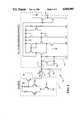
- FIG. 1is a schematic diagram of the present inventive ECL-to-CMOS logic level translator connected at its input to an ECL circuit.
- FIG. 2is a schematic diagram of the present inventive ECL-to-CMOS logic level translator.
- FIG. 3is a schematic diagram of a temperature compensated reference voltage generator present in the aforementioned ECL-to-CMOS logic level translator.
- the arrangement 100 in FIG. 1is a combination of an ECL circuit 102 (evidenced by its bipolar junction transistors) coupled to and ECL-to-CMOS logic level translator 112 (evidenced by its junction field-effect transistors, with a bubble at the gate indicating a p-channel device, and the absence of a bubble at the gate indicating an n-channel device).
- the ECL circuit 102outputs ECL signals over a transmission medium 104, which transmission medium is impedance matched with a resistor 106 (connected to a power source VTT of -2.0 volts) for a maximum signal transfer rate.
- An input line 110carries the ECL signals from the transmission medium 104 to the ECL-to-CMOS logic level translator 112, which translates the ECL signals received into CMOS signals to be output at 114.
- the arrangement 100also contains a circuit 108 for electro-static discharge in order to protect the input to the logic level translator 112 from electro-static charges.
- the transistor in the circuit 108is configured such that it provides low and high voltage electro-static discharge.
- FIG. 2shows the logic level translator 112 in greater detail.
- the input 110 for inputting the ECL signalsconnects a resistor 202, which resistor 202 is connected via node 204 to translator input 210, and to a resistor 206, the resistor 206 being connected to a power source V EE of approximately -5.2 volts.
- the translator input 210supplies the input ECL signal to a differential amplifier 212 which has a reference voltage V REF supplied thereto via line 214 by a temperature compensated reference voltage generator 216.
- the reference voltage suppliedis -2.5 volts at room temperature and is adjusted at a rate of 1 millivolt per degree Celsius.
- the temperature compensated reference voltage generator 216will be described in greater detail infra, with reference to FIG. 3.
- a grounded capacitor 218maintains a steady reference voltage on line 214 when there are unacceptable fluctuations in V EE .
- a differential amplifier output line 220 connected to differential amplifier output node 250introduces a differential output signal to an inverter/gate 222, which inverts the signal received to approximately 0 volts when the signal is below a threshold (-2.5 volts), and inverts the signal received to approximately -5.2 volts when the signal is above the threshold.
- the inverter/gate 222passes inverted signals to the translator output line 114, which signals are now at CMOS logic levels.
- the differential amplifier 212is of the type well-known in the art, and thus will be described only briefly. Having an amplification factor of approximately 10, the differential amplifier 212 has load transistors 230 and 232 whose sources are tied to ground, and which are connected at their gates by line 234. The gates of transistors 230 and 232 are also connected via line 242 to the drains of the transistors 232 and 240. The input transistors 238 and 240 are connected via node 244 to a constant current-source consisting of a transistor 246 having its gate connected to ground, and which is connected at its source to power source V EE . The output of the differential amplifier 212 is carried by a line 220, inverted by the inverter 222, and is finally output at 114.
- the logic level translator 112briefly operates as follows. When a logic high ECL signal is applied to the translator input 110, the resistor 202 shifts that voltage to approximately -2.2 volts at node 204. This turns the transistor 238 on and pulls the line 220 down near -4.0 volts. The voltage on line 220 turns on transistor 224 in the inverter/gate 222 and pulls the output node 226 up to 0 volts. The voltage on line 220 also turns the transistor 228 off at this time. When a logic low ECL signal is applied to the translator input 110, the resistor 202 shifts that voltage to approximately -2.8 volts at node 204, turning the transistor 238 off and placing approximately -1.0 volt on the line 220. This turns the transistor 224 off and the transistor 228 on. The transistor 228 passes the voltage V EE to the output node 226 of the inverter/gate 222.
- the voltages transferred to the output 114are approximately 0 and -5.2 volts.
- the temperature compensated reference voltage generator 216is detailed in FIG. 3.
- Transistors 302(attached to ground via line 304) and 308 (attached to the power source VEE at 310) are chosen such that they place a voltage of -2.5 volts on node 306 at room temperature (25° C. or 77° F.).
- a transistor 312is connected to the node 306 at its source and to ground at its drain. The gate of the transistor 312 is connected via node 316 to a constant voltage source generated by the pair of resistors 314 and 318 (connected to power source VEE at 320).
- the transistor 312is temperature sensitive, and conducts in proportion to the ambient temperature to raise (make it more positive) the voltage at node 306 with increasing temperature.
- the transistor 312increases the reference voltage at node 306 at a rate of 1 millivolt per degree Celsius. The increasing pulling effect with temperature in transistor 312 is due to a decrease in its threshold voltage with increasing temperature.
Landscapes
- Engineering & Computer Science (AREA)
- Computer Hardware Design (AREA)
- Physics & Mathematics (AREA)
- Computing Systems (AREA)
- General Engineering & Computer Science (AREA)
- Mathematical Physics (AREA)
- Logic Circuits (AREA)
Abstract
Description
Claims (10)
Priority Applications (1)
| Application Number | Priority Date | Filing Date | Title |
|---|---|---|---|
| US07/398,856US4968905A (en) | 1989-08-25 | 1989-08-25 | Temperature compensated high speed ECL-to-CMOS logic level translator |
Applications Claiming Priority (1)
| Application Number | Priority Date | Filing Date | Title |
|---|---|---|---|
| US07/398,856US4968905A (en) | 1989-08-25 | 1989-08-25 | Temperature compensated high speed ECL-to-CMOS logic level translator |
Publications (1)
| Publication Number | Publication Date |
|---|---|
| US4968905Atrue US4968905A (en) | 1990-11-06 |
Family
ID=23577063
Family Applications (1)
| Application Number | Title | Priority Date | Filing Date |
|---|---|---|---|
| US07/398,856Expired - LifetimeUS4968905A (en) | 1989-08-25 | 1989-08-25 | Temperature compensated high speed ECL-to-CMOS logic level translator |
Country Status (1)
| Country | Link |
|---|---|
| US (1) | US4968905A (en) |
Cited By (17)
| Publication number | Priority date | Publication date | Assignee | Title |
|---|---|---|---|---|
| US5017812A (en)* | 1990-03-20 | 1991-05-21 | Integrated Device Technology, Inc. | Combined ECL-to-TTL translator and decoder |
| US5075578A (en)* | 1991-01-16 | 1991-12-24 | National Semiconductor Corporation | Input buffer regenerative latch |
| US5101125A (en)* | 1989-04-26 | 1992-03-31 | Kabushiki Kaisha Toshiba | Semiconductor integrated circuit with improved i/o structure with ecl to cmos to ecl conversion |
| US5130576A (en)* | 1991-01-16 | 1992-07-14 | National Semiconductor Corporation | Synchronous ECL to CMOS translator |
| US5160882A (en)* | 1990-03-30 | 1992-11-03 | Texas Instruments Incorporated | Voltage generator having steep temperature coefficient and method of operation |
| US5172017A (en)* | 1991-03-26 | 1992-12-15 | U.S. Philips Corporation | Integrated circuit arrangement including a differential amplifier which generates a constant output voltage over a large temperature range |
| US5202594A (en)* | 1992-02-04 | 1993-04-13 | Motorola, Inc. | Low power level converter |
| US5214328A (en)* | 1990-06-27 | 1993-05-25 | Nec Corporation | ECL to CMOS level conversion circuit |
| US5459427A (en)* | 1994-05-06 | 1995-10-17 | Motorola, Inc. | DC level shifting circuit for analog circuits |
| WO1996031006A1 (en)* | 1995-03-29 | 1996-10-03 | Matra Mhs | Ecl level/cmos level logic signal interfacing device |
| EP0788234A3 (en)* | 1996-01-31 | 1997-12-17 | Nec Corporation | ECL to MOS level conversion circuit using CMOS technologies |
| WO1998008304A1 (en)* | 1996-08-21 | 1998-02-26 | Siemens Aktiengesellschaft | Low-delay signal level converter with protective circuit |
| US6124704A (en)* | 1997-12-02 | 2000-09-26 | U.S. Philips Corporation | Reference voltage source with temperature-compensated output reference voltage |
| US6191619B1 (en) | 1999-08-24 | 2001-02-20 | Analog Devices, Inc. | Translators and methods for converting differential signals to single-ended signals |
| US20060245508A1 (en)* | 2005-05-02 | 2006-11-02 | Seiko Epson Corporation | Receiver circuit, differential signal receiver circuit, interface circuit, and electronic instrument |
| US20090174432A1 (en)* | 2008-01-07 | 2009-07-09 | Honeywell International Inc. | System for Providing a Complementary Metal-Oxide Semiconductor (CMOS) Emitter Coupled Logic (ECL) Equivalent Input/Output (I/O) Circuit |
| US20100007393A1 (en)* | 2008-07-11 | 2010-01-14 | Honeywell International Inc. | Method and Apparatus for Achieving 50% Duty Cycle on the Output VCO of a Phased Locked Loop |
Citations (18)
| Publication number | Priority date | Publication date | Assignee | Title |
|---|---|---|---|---|
| US4242604A (en)* | 1978-08-10 | 1980-12-30 | National Semiconductor Corporation | MOS Input circuit with selectable stabilized trip voltage |
| US4393315A (en)* | 1981-05-18 | 1983-07-12 | Sperry Corporation | High-gain stabilized converter |
| US4437171A (en)* | 1982-01-07 | 1984-03-13 | Intel Corporation | ECL Compatible CMOS memory |
| US4453095A (en)* | 1982-07-16 | 1984-06-05 | Motorola Inc. | ECL MOS Buffer circuits |
| US4533842A (en)* | 1983-12-01 | 1985-08-06 | Advanced Micro Devices, Inc. | Temperature compensated TTL to ECL translator |
| US4563601A (en)* | 1982-09-06 | 1986-01-07 | Hitachi, Ltd. | Level conversion input circuit |
| US4599521A (en)* | 1981-12-29 | 1986-07-08 | Fujitsu Limited | Bias circuit with voltage and temperature compensation for an emitter coupled logic circuit |
| US4656375A (en)* | 1985-12-16 | 1987-04-07 | Ncr Corporation | Temperature compensated CMOS to ECL translator |
| US4698526A (en)* | 1985-10-17 | 1987-10-06 | Inmos Corporation | Source follower CMOS input buffer |
| US4717836A (en)* | 1986-02-04 | 1988-01-05 | Burr-Brown Corporation | CMOS input level shifting circuit with temperature-compensating n-channel field effect transistor structure |
| US4717847A (en)* | 1985-04-29 | 1988-01-05 | Harris Corporation | TTL compatible CMOS input buffer |
| US4719372A (en)* | 1986-02-03 | 1988-01-12 | International Business Machines Corporation | Multiplying interface circuit for level shifting between FET and TTL levels |
| US4736125A (en)* | 1986-08-28 | 1988-04-05 | Applied Micro Circuits Corporation | Unbuffered TTL-to-ECL translator with temperature-compensated threshold voltage obtained from a constant-current reference voltage |
| US4763021A (en)* | 1987-07-06 | 1988-08-09 | Unisys Corporation | CMOS input buffer receiver circuit with ultra stable switchpoint |
| US4767951A (en)* | 1987-06-30 | 1988-08-30 | Hewlett-Packard Company | ECL to NMOS converter |
| US4841175A (en)* | 1987-01-23 | 1989-06-20 | Siemens Aktiengesellschaft | ECL-compatible input/output circuits in CMOS technology |
| US4849660A (en)* | 1987-06-05 | 1989-07-18 | Hitachi, Ltd. | BICMOS output interface circuit for level-shifting ECL to CMOS |
| US4906871A (en)* | 1987-11-26 | 1990-03-06 | Kabushiki Kaisha Toshiba | Level shift circuit for converting a signal in an ecl level into a signal in a cmos logic level |
- 1989
- 1989-08-25USUS07/398,856patent/US4968905A/ennot_activeExpired - Lifetime
Patent Citations (18)
| Publication number | Priority date | Publication date | Assignee | Title |
|---|---|---|---|---|
| US4242604A (en)* | 1978-08-10 | 1980-12-30 | National Semiconductor Corporation | MOS Input circuit with selectable stabilized trip voltage |
| US4393315A (en)* | 1981-05-18 | 1983-07-12 | Sperry Corporation | High-gain stabilized converter |
| US4599521A (en)* | 1981-12-29 | 1986-07-08 | Fujitsu Limited | Bias circuit with voltage and temperature compensation for an emitter coupled logic circuit |
| US4437171A (en)* | 1982-01-07 | 1984-03-13 | Intel Corporation | ECL Compatible CMOS memory |
| US4453095A (en)* | 1982-07-16 | 1984-06-05 | Motorola Inc. | ECL MOS Buffer circuits |
| US4563601A (en)* | 1982-09-06 | 1986-01-07 | Hitachi, Ltd. | Level conversion input circuit |
| US4533842A (en)* | 1983-12-01 | 1985-08-06 | Advanced Micro Devices, Inc. | Temperature compensated TTL to ECL translator |
| US4717847A (en)* | 1985-04-29 | 1988-01-05 | Harris Corporation | TTL compatible CMOS input buffer |
| US4698526A (en)* | 1985-10-17 | 1987-10-06 | Inmos Corporation | Source follower CMOS input buffer |
| US4656375A (en)* | 1985-12-16 | 1987-04-07 | Ncr Corporation | Temperature compensated CMOS to ECL translator |
| US4719372A (en)* | 1986-02-03 | 1988-01-12 | International Business Machines Corporation | Multiplying interface circuit for level shifting between FET and TTL levels |
| US4717836A (en)* | 1986-02-04 | 1988-01-05 | Burr-Brown Corporation | CMOS input level shifting circuit with temperature-compensating n-channel field effect transistor structure |
| US4736125A (en)* | 1986-08-28 | 1988-04-05 | Applied Micro Circuits Corporation | Unbuffered TTL-to-ECL translator with temperature-compensated threshold voltage obtained from a constant-current reference voltage |
| US4841175A (en)* | 1987-01-23 | 1989-06-20 | Siemens Aktiengesellschaft | ECL-compatible input/output circuits in CMOS technology |
| US4849660A (en)* | 1987-06-05 | 1989-07-18 | Hitachi, Ltd. | BICMOS output interface circuit for level-shifting ECL to CMOS |
| US4767951A (en)* | 1987-06-30 | 1988-08-30 | Hewlett-Packard Company | ECL to NMOS converter |
| US4763021A (en)* | 1987-07-06 | 1988-08-09 | Unisys Corporation | CMOS input buffer receiver circuit with ultra stable switchpoint |
| US4906871A (en)* | 1987-11-26 | 1990-03-06 | Kabushiki Kaisha Toshiba | Level shift circuit for converting a signal in an ecl level into a signal in a cmos logic level |
Cited By (22)
| Publication number | Priority date | Publication date | Assignee | Title |
|---|---|---|---|---|
| US5101125A (en)* | 1989-04-26 | 1992-03-31 | Kabushiki Kaisha Toshiba | Semiconductor integrated circuit with improved i/o structure with ecl to cmos to ecl conversion |
| US5017812A (en)* | 1990-03-20 | 1991-05-21 | Integrated Device Technology, Inc. | Combined ECL-to-TTL translator and decoder |
| US5160882A (en)* | 1990-03-30 | 1992-11-03 | Texas Instruments Incorporated | Voltage generator having steep temperature coefficient and method of operation |
| US5214328A (en)* | 1990-06-27 | 1993-05-25 | Nec Corporation | ECL to CMOS level conversion circuit |
| US5075578A (en)* | 1991-01-16 | 1991-12-24 | National Semiconductor Corporation | Input buffer regenerative latch |
| US5130576A (en)* | 1991-01-16 | 1992-07-14 | National Semiconductor Corporation | Synchronous ECL to CMOS translator |
| US5172017A (en)* | 1991-03-26 | 1992-12-15 | U.S. Philips Corporation | Integrated circuit arrangement including a differential amplifier which generates a constant output voltage over a large temperature range |
| US5202594A (en)* | 1992-02-04 | 1993-04-13 | Motorola, Inc. | Low power level converter |
| US5459427A (en)* | 1994-05-06 | 1995-10-17 | Motorola, Inc. | DC level shifting circuit for analog circuits |
| WO1996031006A1 (en)* | 1995-03-29 | 1996-10-03 | Matra Mhs | Ecl level/cmos level logic signal interfacing device |
| EP0788234A3 (en)* | 1996-01-31 | 1997-12-17 | Nec Corporation | ECL to MOS level conversion circuit using CMOS technologies |
| WO1998008304A1 (en)* | 1996-08-21 | 1998-02-26 | Siemens Aktiengesellschaft | Low-delay signal level converter with protective circuit |
| US6124704A (en)* | 1997-12-02 | 2000-09-26 | U.S. Philips Corporation | Reference voltage source with temperature-compensated output reference voltage |
| US6191619B1 (en) | 1999-08-24 | 2001-02-20 | Analog Devices, Inc. | Translators and methods for converting differential signals to single-ended signals |
| US20060245508A1 (en)* | 2005-05-02 | 2006-11-02 | Seiko Epson Corporation | Receiver circuit, differential signal receiver circuit, interface circuit, and electronic instrument |
| EP1720256A3 (en)* | 2005-05-02 | 2007-02-21 | Seiko Epson Corporation | Line receiver circuit |
| US7408385B2 (en) | 2005-05-02 | 2008-08-05 | Seiko Epson Corporation | Receiver circuit, differential signal receiver circuit, interface circuit, and electronic instrument |
| US20090174432A1 (en)* | 2008-01-07 | 2009-07-09 | Honeywell International Inc. | System for Providing a Complementary Metal-Oxide Semiconductor (CMOS) Emitter Coupled Logic (ECL) Equivalent Input/Output (I/O) Circuit |
| US7688110B2 (en)* | 2008-01-07 | 2010-03-30 | Honeywell International, Inc. | System for providing a complementary metal-oxide semiconductor (CMOS) emitter coupled logic (ECL) equivalent input/output (I/O) circuit |
| EP2077619A3 (en)* | 2008-01-07 | 2012-04-04 | Honeywell International Inc. | System for providing a complementary metal-oxide semiconductor (CMOS) emitter coupled logic (ECL) equivalent input/output (I/O) circuit |
| US20100007393A1 (en)* | 2008-07-11 | 2010-01-14 | Honeywell International Inc. | Method and Apparatus for Achieving 50% Duty Cycle on the Output VCO of a Phased Locked Loop |
| US7965118B2 (en) | 2008-07-11 | 2011-06-21 | Honeywell International Inc. | Method and apparatus for achieving 50% duty cycle on the output VCO of a phased locked loop |
Similar Documents
| Publication | Publication Date | Title |
|---|---|---|
| US4968905A (en) | Temperature compensated high speed ECL-to-CMOS logic level translator | |
| US5568065A (en) | Circuit for connecting a node to a voltage source selected from alternative voltage sources | |
| US5204557A (en) | Digital signal level translator | |
| KR940006965B1 (en) | Output circuit | |
| US4477737A (en) | Voltage generator circuit having compensation for process and temperature variation | |
| US5546020A (en) | Data output buffer with latch up prevention | |
| US5926056A (en) | Voltage tolerant output buffer | |
| US5574389A (en) | CMOS 3.3 volt output buffer with 5 volt protection | |
| US5434518A (en) | ECL-to-BICOMS/CMOS translator | |
| US5966032A (en) | BiCMOS transceiver (driver and receiver) for gigahertz operation | |
| DE59205707D1 (en) | Integrated buffer circuit | |
| US4704549A (en) | CMOS to ECL converter-buffer | |
| US5120993A (en) | Substrate bias voltage detection circuit | |
| US5537066A (en) | Flip-flop type amplifier circuit | |
| US5973530A (en) | Low power, high voltage-tolerant bus holder circuit in low voltage technology | |
| US6483386B1 (en) | Low voltage differential amplifier with high voltage protection | |
| US7230469B2 (en) | Multi-level/single ended input level shifter circuit | |
| KR100197998B1 (en) | Low power loss input buffer of semiconductor device | |
| US6327190B1 (en) | Complementary differential input buffer for a semiconductor memory device | |
| US4890051A (en) | CMOS input buffer stable for the variation of a power supplying voltage | |
| US6127848A (en) | Voltage translator with gate oxide breakdown protection | |
| US5359240A (en) | Low power digital signal buffer circuit | |
| US4888501A (en) | ECL to CMOS converter | |
| US5739702A (en) | Bus hold circuit | |
| US5189318A (en) | Analog signal extracting circuit |
Legal Events
| Date | Code | Title | Description |
|---|---|---|---|
| AS | Assignment | Owner name:NCR CORPORATION, DAYTON, OHIO, A CORP. OF MD. Free format text:ASSIGNMENT OF ASSIGNORS INTEREST.;ASSIGNORS:SANWO, IKUO J.;MILBY, GREGORY H.;LE, QUYNH-GIAO X.;REEL/FRAME:005153/0024 Effective date:19890808 | |
| STCF | Information on status: patent grant | Free format text:PATENTED CASE | |
| AS | Assignment | Owner name:BRITISH AEROSPACE PUBLIC LIMITED COMPANY, 11 STRAN Free format text:ASSIGNMENT OF ASSIGNORS INTEREST.;ASSIGNORS:DOBIE, WILLIAM B. S.;PENISTONE, NIGEL;REEL/FRAME:005610/0089;SIGNING DATES FROM 19890926 TO 19891002 | |
| FPAY | Fee payment | Year of fee payment:4 | |
| FPAY | Fee payment | Year of fee payment:8 | |
| FPAY | Fee payment | Year of fee payment:12 | |
| AS | Assignment | Owner name:STEINMETZ ELECTRICAL LLC, CALIFORNIA Free format text:ASSIGNMENT OF ASSIGNORS INTEREST;ASSIGNOR:NCR CORPORATION;REEL/FRAME:015428/0845 Effective date:20040623 | |
| FEPP | Fee payment procedure | Free format text:PAYER NUMBER DE-ASSIGNED (ORIGINAL EVENT CODE: RMPN); ENTITY STATUS OF PATENT OWNER: LARGE ENTITY Free format text:PAYOR NUMBER ASSIGNED (ORIGINAL EVENT CODE: ASPN); ENTITY STATUS OF PATENT OWNER: LARGE ENTITY |