US4968628A - Method of fabricating back diffused bonded oxide substrates - Google Patents
Method of fabricating back diffused bonded oxide substratesDownload PDFInfo
- Publication number
- US4968628A US4968628AUS07/282,064US28206488AUS4968628AUS 4968628 AUS4968628 AUS 4968628AUS 28206488 AUS28206488 AUS 28206488AUS 4968628 AUS4968628 AUS 4968628A
- Authority
- US
- United States
- Prior art keywords
- alignment
- moat
- forming
- mask
- substrate
- Prior art date
- Legal status (The legal status is an assumption and is not a legal conclusion. Google has not performed a legal analysis and makes no representation as to the accuracy of the status listed.)
- Expired - Lifetime
Links
Images

Classifications
- H—ELECTRICITY
- H01—ELECTRIC ELEMENTS
- H01L—SEMICONDUCTOR DEVICES NOT COVERED BY CLASS H10
- H01L21/00—Processes or apparatus adapted for the manufacture or treatment of semiconductor or solid state devices or of parts thereof
- H01L21/70—Manufacture or treatment of devices consisting of a plurality of solid state components formed in or on a common substrate or of parts thereof; Manufacture of integrated circuit devices or of parts thereof
- H01L21/71—Manufacture of specific parts of devices defined in group H01L21/70
- H01L21/76—Making of isolation regions between components
- H01L21/762—Dielectric regions, e.g. EPIC dielectric isolation, LOCOS; Trench refilling techniques, SOI technology, use of channel stoppers
- H01L21/7624—Dielectric regions, e.g. EPIC dielectric isolation, LOCOS; Trench refilling techniques, SOI technology, use of channel stoppers using semiconductor on insulator [SOI] technology
- H01L21/76251—Dielectric regions, e.g. EPIC dielectric isolation, LOCOS; Trench refilling techniques, SOI technology, use of channel stoppers using semiconductor on insulator [SOI] technology using bonding techniques
- Y—GENERAL TAGGING OF NEW TECHNOLOGICAL DEVELOPMENTS; GENERAL TAGGING OF CROSS-SECTIONAL TECHNOLOGIES SPANNING OVER SEVERAL SECTIONS OF THE IPC; TECHNICAL SUBJECTS COVERED BY FORMER USPC CROSS-REFERENCE ART COLLECTIONS [XRACs] AND DIGESTS
- Y10—TECHNICAL SUBJECTS COVERED BY FORMER USPC
- Y10S—TECHNICAL SUBJECTS COVERED BY FORMER USPC CROSS-REFERENCE ART COLLECTIONS [XRACs] AND DIGESTS
- Y10S148/00—Metal treatment
- Y10S148/012—Bonding, e.g. electrostatic for strain gauges
- Y—GENERAL TAGGING OF NEW TECHNOLOGICAL DEVELOPMENTS; GENERAL TAGGING OF CROSS-SECTIONAL TECHNOLOGIES SPANNING OVER SEVERAL SECTIONS OF THE IPC; TECHNICAL SUBJECTS COVERED BY FORMER USPC CROSS-REFERENCE ART COLLECTIONS [XRACs] AND DIGESTS
- Y10—TECHNICAL SUBJECTS COVERED BY FORMER USPC
- Y10S—TECHNICAL SUBJECTS COVERED BY FORMER USPC CROSS-REFERENCE ART COLLECTIONS [XRACs] AND DIGESTS
- Y10S438/00—Semiconductor device manufacturing: process
- Y10S438/928—Front and rear surface processing
Definitions
- the present inventionrelates generally to a method of fabricating dielectrically isolated regions, and more specifically to an improved method of fabricating back diffused bonded oxide substrates having dielectrically isolated islands.
- Devices in integrated circuitsare formed by introducing impurities into a surface of a substrate. This requires the use of a plurality of masks to form regions of different depths and impurity concentrations. Acceptability of the finally formed devices depends upon alignment of the diffused regions. Thus, there is a great emphasis on schemes to align a mask to a substrate to assure proper alignment of the diffused regions.
- the first diffusionis from a top or front surface and consequently, all the diffusions may be aligned relative to the first diffusion.
- This techniquemay include positioning an indicia on a substrate and performing the first and subsequent diffusions using an indicia on the mask to align with the indicia on the substrate.
- the dielectrically isolated islandsare formed from a first surface which subsequently becomes a buried surface and the devices are formed therein by diffusion into a second surface opposite the first surface which does not exist in the initial material.
- no initial markmay be formed which allows alignment of the diffused device regions to the dielectric isolation. Since it is unacceptable in some applications for diffused regions of the device to touch the dielectric isolation, more care and time have to be used to align the mask relative to the dielectric isolation. Since the islands have inwardly sloping sides, the surface area available for forming the diffused regions is a function of the amount of starting material removed.
- the size of the islands as perceived from the surfacevaries considerably.
- the diffusionsare aligned to the outside of the islands.
- the alignment in a possibly increased islandwill not assure alignment in the remaining islands on the wafer.
- the varied island sizealso results in a varying alignment tolerance. This causes difficulty in judging alignment visually.
- a support material rectangular indiciais formed during the formation of the dielectric isolation of starting material islands in one of the dielectrically isolated islands as described in U.S. Pat. No. 4,309,812 to Hull.
- the resulting indiciaappears on the front processing face during the thinning of the substrate to produce the dielectrically isolated islands.
- An X indicia on a maskis positioned over the four corners of the rectangular indicia to align the mask and substrate for subsequent processing.
- the rectangular indiciais not used for any back side processing, only front side processing since it is formed with the isolation moats.
- SOIsemiconductor-on-insulator
- a thin substrateis separated from a handle wafer by an insulator layer.
- These structuresmay be formed by high dose oxygen implantation (SIMOX), bonded wafers, ZMR or full isolation by porous oxidation silicon (FIPOS) These processes generally do not include backside processing, and any buried layers are produced by epitaxial deposition of the resulting substrate over the buried layer regions.
- Another object of the present inventionis to provide a semiconductor-on-insulator integrated circuit with backside processing and improved alignment.
- an alignment moat of a first depth on a first surface of a substrateand performing all backside processing using the alignment moat, forming a first oxide layer on the first surface and bonding it to a handle wafer by oxide bonding.
- the substrateis then thinned from a second surface opposite the first surface down to a thickness less than the depth of the alignment moat so the alignment moat is exposed at a third surface.
- Isolationeither dielectric or junction, is then formed in the third surface extending down through the substrate to the first oxide layer.
- Topside processingis then conducted. While anisotropic chemical etching is used to form the alignment moat so as to provide a depth indicator, the dielectric isolation trenches are formed by reactive ion etching.
- the backside processingincludes diffusing impurities having an opposite conductivity type than that of the substrate to a depth at least equal to the depth of the alignment moat. Impurities to form a buried region, which are the same conductivity type as the substrate, are formed to a depth substantially less than the alignment moat depth. If a non-oxide mask is used as the last masking step in the backside processing, an additional oxide layer may be formed prior to bonding. If an oxide mask is used as the last mask in the backside processing, it must be stripped and a fresh layer of oxide must be applied to the first or back surface prior to bonding.
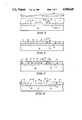
- FIGS. 1-8show cross-sectional views of a wafer during various stages of fabrication according to the principles of the present invention, with FIGS. 3a and 3b being alternative steps in that process.
- a beginning substrate 10for example having an N-impurity concentration and a thickness exceeding 5 mils, includes a first surface 12 and an opposed second surface 14.
- the surface 12has a mask layer 16 applied with a mask opening 18.
- the substrate 10is then etched to form an alignment moat 20.
- an anisotropic etchis performed such that the depth of the alignment moat 20 which is in the range of 5 to 30 microns is defined by the size of the opening 18 in the mask layer 16.
- the alignment moat 20may also act as a depth indicator to be used in subsequent processing.
- the mask layer 16is preferably a silicon dioxide. The substrate at this stage is illustrated in FIG. 1.
- the masking layer 16is removed and a thin layer of oxide 22 is formed on a surface 12 and in the moat 20 of the substrate 10. This thin oxide layer is in the range of approximately 1,000 angstroms.
- a mask layer 24is formed therein with an aperture 26 therein using the alignment moat 20. P-type impurities, for example boron, are introduced through the aperture 26 as illustrated in FIG. 2.
- the mask layer 24, which may be photoresist,is removed.
- the waferis then subjected to a high temperature diffusion resulting in P-region 28 which will become the P collectors, as illustrated in FIGS. 3a and 3b.
- a mask layer 30is then formed on the surface 12 with an aperture 32 therein using the alignment moat 20.
- N-type impuritiesfor example arsenic, is ion implanted to form a buried layer 34 as can be seen in FIG. 4.
- One method of forming the mask layer 30is to expose the substrate to an oxidizing atmosphere or chemical vapor deposit the oxide layer, as illustrated in FIG. 3a.
- the original oxide 22is shown not removed prior to forming mask layer 30, but can be stripped after the high temperature diffusion.
- An alternativewould be to use a non-oxide mask layer 30' of materials, for example nitride or a metal such as aluminum, as illustrated in FIG. 3b. In this case the original oxide layer 22 or a new thin oxide layer must be applied prior to mask layer 30'.
- the ion implantationis through the thin oxide layer 22 in the aperture 32. After the ion implantation of N-type impurities, the mask layer 30, 30' is removed.
- the mask layer 30is an oxide
- the original thin oxide layer 22 and 30are removed simultaneously.
- the mask layer 30'is a non-oxide, it can be selectively removed, leaving the clean thin layer 22 on the surface 12.
- the thin layer 22may then be used for the subsequent bonding steps. If the mask 30' is an oxide and layer 22 is removed, the surface 12 must have an oxide layer applied thereto by thermal or chemical vapor deposition resulting in a layer 36 as illustrated in FIG. 4.
- the thin layer 36, 22is in the 10-1000 angstrom range.
- a handle wafer 40 having an oxide layer 42 thereonis then positioned on the surface 12 with its oxide layer 36, 22 contacting the oxide layer 42 of the handle wafer 40.
- the wafersare then taken to a high temperature, for example greater than 1000° C., and held there for more than one hour. This causes the oxide layers to bond, thereby joining the wafer 40 to the substrate 10.
- the resulting productis illustrated in FIG. 5.
- the resulting combined thickness of layers 42, 36 and 22define the desired dielectric isolation thickness which is in the range of 1 to 4 microns.
- the N-type impuritiesform buried region 34.
- the substrate 10is then thinned by removing materials from the surface 14 by grinding or electro-chemical etching, as described in U.S. Pat. No. 4,554,059 to Short et al., to reduce the thickness of the substrate 10 equal to or below that of the depth of the alignment moat 20.
- the new surface 38as illustrated in FIG. 6, exposes the moat 20, as well as intersecting the P- region 28.
- the P- region 28extends from the surface 38 to 12 as well as the moat 20 extending between surfaces 38 and 12.
- the N- region 34becomes a buried layer at surface 12.
- the ultimate depth of region 28 with all the heat stepsis in the range of 10 to 40 microns such that it exceeds the precisely developed depth of the alignment moat 20 which is in the range of 5 to 30 microns. This assures that when the thinning of the substrate 10 is performed, the region 28 extends between the surface 12 and surface 38, producing a uniform doping profile.
- Topside processingthen commences with forming a masking layer 44, for example an oxide which is patterned using photoresist, on the new top layer 38 and in the alignment moats 20.
- Isolation apertures 46are formed in the mask layer 44 as illustrated in FIG. 7.
- Reactive ion etchingis then performed to form isolation trenches 50 therein, as well as clearing the alignment moat 20.
- the trenches 50 and alignment 20extend from the top surface 38 down to the bottom surface 12 and the insulative layer 42, as illustrated in FIG. 8.
- the processing of the substrate of FIG. 8is well known, including filling the moats 50 with an insulative layer and planarizing, and subsequently forming devices in the dielectric isolated regions of substrate 10 and region 28.
- lateral isolationare dielectric trenches
- lateral junction isolationmay also be used. This may include forming P-type regions extending between surface 12 and 38 by front or back side processing.
- a backside alignment moatfurnishes backside alignment marks, depth indicator and a front to back alignment device while allowing integration of backside diffusions to a bonded wafer process.
Landscapes
- Engineering & Computer Science (AREA)
- Physics & Mathematics (AREA)
- Condensed Matter Physics & Semiconductors (AREA)
- General Physics & Mathematics (AREA)
- Manufacturing & Machinery (AREA)
- Computer Hardware Design (AREA)
- Microelectronics & Electronic Packaging (AREA)
- Power Engineering (AREA)
- Element Separation (AREA)
Abstract
Description
Claims (19)
Priority Applications (1)
| Application Number | Priority Date | Filing Date | Title |
|---|---|---|---|
| US07/282,064US4968628A (en) | 1988-12-09 | 1988-12-09 | Method of fabricating back diffused bonded oxide substrates |
Applications Claiming Priority (1)
| Application Number | Priority Date | Filing Date | Title |
|---|---|---|---|
| US07/282,064US4968628A (en) | 1988-12-09 | 1988-12-09 | Method of fabricating back diffused bonded oxide substrates |
Publications (1)
| Publication Number | Publication Date |
|---|---|
| US4968628Atrue US4968628A (en) | 1990-11-06 |
Family
ID=23079955
Family Applications (1)
| Application Number | Title | Priority Date | Filing Date |
|---|---|---|---|
| US07/282,064Expired - LifetimeUS4968628A (en) | 1988-12-09 | 1988-12-09 | Method of fabricating back diffused bonded oxide substrates |
Country Status (1)
| Country | Link |
|---|---|
| US (1) | US4968628A (en) |
Cited By (19)
| Publication number | Priority date | Publication date | Assignee | Title |
|---|---|---|---|---|
| US5026437A (en)* | 1990-01-22 | 1991-06-25 | Tencor Instruments | Cantilevered microtip manufacturing by ion implantation and etching |
| US5164218A (en)* | 1989-05-12 | 1992-11-17 | Nippon Soken, Inc. | Semiconductor device and a method for producing the same |
| US5234860A (en)* | 1992-03-19 | 1993-08-10 | Eastman Kodak Company | Thinning of imaging device processed wafers |
| US5234535A (en)* | 1992-12-10 | 1993-08-10 | International Business Machines Corporation | Method of producing a thin silicon-on-insulator layer |
| US5374329A (en)* | 1992-01-31 | 1994-12-20 | Canon Kabushiki Kaisha | Process for producing a semiconductor wafer |
| US5470782A (en)* | 1993-12-02 | 1995-11-28 | Siemens Aktiengesellschaft | Method for manufacturing an integrated circuit arrangement |
| US5488012A (en)* | 1993-10-18 | 1996-01-30 | The Regents Of The University Of California | Silicon on insulator with active buried regions |
| US5496764A (en)* | 1994-07-05 | 1996-03-05 | Motorola, Inc. | Process for forming a semiconductor region adjacent to an insulating layer |
| EP0543361A3 (en)* | 1991-11-20 | 1997-09-03 | Canon Kk | Semiconductor device and method of manufacturing the same |
| US5691231A (en)* | 1994-06-16 | 1997-11-25 | Nec Corporation | Method of manufacturing silicon on insulating substrate |
| US5888838A (en)* | 1998-06-04 | 1999-03-30 | International Business Machines Corporation | Method and apparatus for preventing chip breakage during semiconductor manufacturing using wafer grinding striation information |
| US5913130A (en)* | 1996-06-12 | 1999-06-15 | Harris Corporation | Method for fabricating a power device |
| US6037239A (en)* | 1997-04-23 | 2000-03-14 | Elantec, Inc. | Method for making a contact structure for a polysilicon filled trench isolation |
| US6096621A (en)* | 1997-04-23 | 2000-08-01 | Elantec, Inc. | Polysilicon filled trench isolation structure for soi integrated circuits |
| WO2000016041A3 (en)* | 1998-09-12 | 2000-09-28 | Secr Defence | Formation of suspended beams using soi substrates, and application to the fabrication of a vibrating gyrometer |
| US6140205A (en)* | 1997-04-23 | 2000-10-31 | Elantec, Inc. | Method of forming retrograde well in bonded waffers |
| US6403447B1 (en) | 1999-07-07 | 2002-06-11 | Elantec Semiconductor, Inc. | Reduced substrate capacitance high performance SOI process |
| US6534381B2 (en)* | 1999-01-08 | 2003-03-18 | Silicon Genesis Corporation | Method for fabricating multi-layered substrates |
| US20040033676A1 (en)* | 2002-04-23 | 2004-02-19 | Stmicroelectronics S.A. | Electronic components and method of fabricating the same |
Citations (9)
| Publication number | Priority date | Publication date | Assignee | Title |
|---|---|---|---|---|
| US3689357A (en)* | 1970-12-10 | 1972-09-05 | Gen Motors Corp | Glass-polysilicon dielectric isolation |
| US3865649A (en)* | 1972-10-16 | 1975-02-11 | Harris Intertype Corp | Fabrication of MOS devices and complementary bipolar transistor devices in a monolithic substrate |
| US4309813A (en)* | 1979-12-26 | 1982-01-12 | Harris Corporation | Mask alignment scheme for laterally and totally dielectrically isolated integrated circuits |
| US4312680A (en)* | 1980-03-31 | 1982-01-26 | Rca Corporation | Method of manufacturing submicron channel transistors |
| US4554059A (en)* | 1983-11-04 | 1985-11-19 | Harris Corporation | Electrochemical dielectric isolation technique |
| JPS61139041A (en)* | 1984-12-10 | 1986-06-26 | Matsushita Electric Works Ltd | Manufacture of di (dielectric isolation) substrate |
| US4638552A (en)* | 1984-05-09 | 1987-01-27 | Kabushiki Kaisha Toshiba | Method of manufacturing semiconductor substrate |
| US4784970A (en)* | 1987-11-18 | 1988-11-15 | Grumman Aerospace Corporation | Process for making a double wafer moated signal processor |
| US4851078A (en)* | 1987-06-29 | 1989-07-25 | Harris Corporation | Dielectric isolation process using double wafer bonding |
- 1988
- 1988-12-09USUS07/282,064patent/US4968628A/ennot_activeExpired - Lifetime
Patent Citations (9)
| Publication number | Priority date | Publication date | Assignee | Title |
|---|---|---|---|---|
| US3689357A (en)* | 1970-12-10 | 1972-09-05 | Gen Motors Corp | Glass-polysilicon dielectric isolation |
| US3865649A (en)* | 1972-10-16 | 1975-02-11 | Harris Intertype Corp | Fabrication of MOS devices and complementary bipolar transistor devices in a monolithic substrate |
| US4309813A (en)* | 1979-12-26 | 1982-01-12 | Harris Corporation | Mask alignment scheme for laterally and totally dielectrically isolated integrated circuits |
| US4312680A (en)* | 1980-03-31 | 1982-01-26 | Rca Corporation | Method of manufacturing submicron channel transistors |
| US4554059A (en)* | 1983-11-04 | 1985-11-19 | Harris Corporation | Electrochemical dielectric isolation technique |
| US4638552A (en)* | 1984-05-09 | 1987-01-27 | Kabushiki Kaisha Toshiba | Method of manufacturing semiconductor substrate |
| JPS61139041A (en)* | 1984-12-10 | 1986-06-26 | Matsushita Electric Works Ltd | Manufacture of di (dielectric isolation) substrate |
| US4851078A (en)* | 1987-06-29 | 1989-07-25 | Harris Corporation | Dielectric isolation process using double wafer bonding |
| US4784970A (en)* | 1987-11-18 | 1988-11-15 | Grumman Aerospace Corporation | Process for making a double wafer moated signal processor |
Cited By (28)
| Publication number | Priority date | Publication date | Assignee | Title |
|---|---|---|---|---|
| US5164218A (en)* | 1989-05-12 | 1992-11-17 | Nippon Soken, Inc. | Semiconductor device and a method for producing the same |
| US5026437A (en)* | 1990-01-22 | 1991-06-25 | Tencor Instruments | Cantilevered microtip manufacturing by ion implantation and etching |
| US5952694A (en)* | 1991-11-20 | 1999-09-14 | Canon Kabushiki Kaisha | Semiconductor device made using processing from both sides of a workpiece |
| EP0543361A3 (en)* | 1991-11-20 | 1997-09-03 | Canon Kk | Semiconductor device and method of manufacturing the same |
| US6329265B1 (en)* | 1991-11-20 | 2001-12-11 | Canon Kabushiki Kaisha | Method of making a semiconductor device using processing from both sides of a workpiece |
| US5374329A (en)* | 1992-01-31 | 1994-12-20 | Canon Kabushiki Kaisha | Process for producing a semiconductor wafer |
| US5234860A (en)* | 1992-03-19 | 1993-08-10 | Eastman Kodak Company | Thinning of imaging device processed wafers |
| US5234535A (en)* | 1992-12-10 | 1993-08-10 | International Business Machines Corporation | Method of producing a thin silicon-on-insulator layer |
| US5488012A (en)* | 1993-10-18 | 1996-01-30 | The Regents Of The University Of California | Silicon on insulator with active buried regions |
| US5470782A (en)* | 1993-12-02 | 1995-11-28 | Siemens Aktiengesellschaft | Method for manufacturing an integrated circuit arrangement |
| US5691231A (en)* | 1994-06-16 | 1997-11-25 | Nec Corporation | Method of manufacturing silicon on insulating substrate |
| US5496764A (en)* | 1994-07-05 | 1996-03-05 | Motorola, Inc. | Process for forming a semiconductor region adjacent to an insulating layer |
| US5913130A (en)* | 1996-06-12 | 1999-06-15 | Harris Corporation | Method for fabricating a power device |
| US6078077A (en)* | 1996-06-12 | 2000-06-20 | Intersil Corporation | Power device |
| US6236083B1 (en) | 1996-06-12 | 2001-05-22 | Intersil Corporation | Power device |
| US6037239A (en)* | 1997-04-23 | 2000-03-14 | Elantec, Inc. | Method for making a contact structure for a polysilicon filled trench isolation |
| US6096621A (en)* | 1997-04-23 | 2000-08-01 | Elantec, Inc. | Polysilicon filled trench isolation structure for soi integrated circuits |
| US6140205A (en)* | 1997-04-23 | 2000-10-31 | Elantec, Inc. | Method of forming retrograde well in bonded waffers |
| US5888838A (en)* | 1998-06-04 | 1999-03-30 | International Business Machines Corporation | Method and apparatus for preventing chip breakage during semiconductor manufacturing using wafer grinding striation information |
| US6171873B1 (en) | 1998-06-04 | 2001-01-09 | International Business Machines Corporation | Method and apparatus for preventing chip breakage during semiconductor manufacturing using wafer grinding striation information |
| US6276205B1 (en) | 1998-09-12 | 2001-08-21 | The Secretary Of State For Defence In Her Britanic Majesty's Government Of The United Kingdom Of Great Britain And Northern Ireland | Micro-machining |
| WO2000016041A3 (en)* | 1998-09-12 | 2000-09-28 | Secr Defence | Formation of suspended beams using soi substrates, and application to the fabrication of a vibrating gyrometer |
| US6670212B2 (en) | 1998-09-12 | 2003-12-30 | Qinetiq Limited | Micro-machining |
| US6534381B2 (en)* | 1999-01-08 | 2003-03-18 | Silicon Genesis Corporation | Method for fabricating multi-layered substrates |
| US6403447B1 (en) | 1999-07-07 | 2002-06-11 | Elantec Semiconductor, Inc. | Reduced substrate capacitance high performance SOI process |
| US6617646B2 (en) | 1999-07-07 | 2003-09-09 | Elantec Semiconductor, Inc. | Reduced substrate capacitance high performance SOI process |
| US20040033676A1 (en)* | 2002-04-23 | 2004-02-19 | Stmicroelectronics S.A. | Electronic components and method of fabricating the same |
| US7214597B2 (en)* | 2002-04-23 | 2007-05-08 | Stmicroelectronics S.A. | Electronic components and method of fabricating the same |
Similar Documents
| Publication | Publication Date | Title |
|---|---|---|
| US4968628A (en) | Method of fabricating back diffused bonded oxide substrates | |
| US4897362A (en) | Double epitaxial method of fabricating semiconductor devices on bonded wafers | |
| US6174784B1 (en) | Technique for producing small islands of silicon on insulator | |
| US6211039B1 (en) | Silicon-on-insulator islands and method for their formation | |
| US5476813A (en) | Method of manufacturing a bonded semiconductor substrate and a dielectric isolated bipolar transistor | |
| EP0036111B1 (en) | Method for making fine deep dielectric isolation | |
| US5681775A (en) | Soi fabrication process | |
| US4187125A (en) | Method for manufacturing semiconductor structures by anisotropic and isotropic etching | |
| US4018627A (en) | Method for fabricating semiconductor devices utilizing oxide protective layer | |
| US4389294A (en) | Method for avoiding residue on a vertical walled mesa | |
| EP0276292A1 (en) | METHOD FOR MANUFACTURING MOS STACKED STRUCTURES. | |
| US3972754A (en) | Method for forming dielectric isolation in integrated circuits | |
| US5395789A (en) | Integrated circuit with self-aligned isolation | |
| US4731343A (en) | Method for manufacturing insulation separating the active regions of a VLSI CMOS circuit | |
| US5389569A (en) | Vertical and lateral isolation for a semiconductor device | |
| JPS6123657B2 (en) | ||
| KR100582147B1 (en) | Semiconductor ic apparatus and method for fabricating the same | |
| KR910000020B1 (en) | Manufacturing Method of Semiconductor Device | |
| US4586243A (en) | Method for more uniformly spacing features in a semiconductor monolithic integrated circuit | |
| US5851901A (en) | Method of manufacturing an isolation region of a semiconductor device with advanced planarization | |
| EP0140749A1 (en) | Method for producing a complementary semiconductor device with a dielectric isolation structure | |
| US4546537A (en) | Method for producing a semiconductor device utilizing V-groove etching and thermal oxidation | |
| KR0172724B1 (en) | Method of manufacturing field oxide film on the semiconductor device | |
| US4544940A (en) | Method for more uniformly spacing features in a lateral bipolar transistor | |
| JPH0661343A (en) | Manufacture of semiconductor device |
Legal Events
| Date | Code | Title | Description |
|---|---|---|---|
| AS | Assignment | Owner name:HARRIS CORPORATION, MELBOURNE, FLORIDA 32919, U.S. Free format text:ASSIGNMENT OF ASSIGNORS INTEREST.;ASSIGNORS:DELGADO, JOSE A.;GAUL, STEPHEN J.;MC LACHLAN, CRAIG J.;AND OTHERS;REEL/FRAME:004988/0359 Effective date:19881205 Owner name:HARRIS CORPORATION, A CORP. OF DE., FLORIDA Free format text:ASSIGNMENT OF ASSIGNORS INTEREST;ASSIGNORS:DELGADO, JOSE A.;GAUL, STEPHEN J.;MC LACHLAN, CRAIG J.;AND OTHERS;REEL/FRAME:004988/0359 Effective date:19881205 | |
| STCF | Information on status: patent grant | Free format text:PATENTED CASE | |
| FEPP | Fee payment procedure | Free format text:PAYOR NUMBER ASSIGNED (ORIGINAL EVENT CODE: ASPN); ENTITY STATUS OF PATENT OWNER: LARGE ENTITY | |
| FPAY | Fee payment | Year of fee payment:4 | |
| FPAY | Fee payment | Year of fee payment:8 | |
| AS | Assignment | Owner name:INTERSIL CORPORATION, FLORIDA Free format text:ASSIGNMENT OF ASSIGNORS INTEREST;ASSIGNOR:HARRIS CORPORATION;REEL/FRAME:010247/0043 Effective date:19990813 | |
| AS | Assignment | Owner name:CREDIT SUISSE FIRST BOSTON, AS COLLATERAL AGENT, N Free format text:SECURITY INTEREST;ASSIGNOR:INTERSIL CORPORATION;REEL/FRAME:010351/0410 Effective date:19990813 | |
| FPAY | Fee payment | Year of fee payment:12 | |
| REMI | Maintenance fee reminder mailed |