US4967243A - Power transistor structure with high speed integral antiparallel Schottky diode - Google Patents
Power transistor structure with high speed integral antiparallel Schottky diodeDownload PDFInfo
- Publication number
- US4967243A US4967243AUS07/221,482US22148288AUS4967243AUS 4967243 AUS4967243 AUS 4967243AUS 22148288 AUS22148288 AUS 22148288AUS 4967243 AUS4967243 AUS 4967243A
- Authority
- US
- United States
- Prior art keywords
- layer
- base region
- region
- base
- reverse
- Prior art date
- Legal status (The legal status is an assumption and is not a legal conclusion. Google has not performed a legal analysis and makes no representation as to the accuracy of the status listed.)
- Expired - Lifetime
Links
Images


Classifications
- H—ELECTRICITY
- H10—SEMICONDUCTOR DEVICES; ELECTRIC SOLID-STATE DEVICES NOT OTHERWISE PROVIDED FOR
- H10D—INORGANIC ELECTRIC SEMICONDUCTOR DEVICES
- H10D84/00—Integrated devices formed in or on semiconductor substrates that comprise only semiconducting layers, e.g. on Si wafers or on GaAs-on-Si wafers
- H10D84/101—Integrated devices comprising main components and built-in components, e.g. IGBT having built-in freewheel diode
- H10D84/141—VDMOS having built-in components
- H10D84/146—VDMOS having built-in components the built-in components being Schottky barrier diodes
- H—ELECTRICITY
- H10—SEMICONDUCTOR DEVICES; ELECTRIC SOLID-STATE DEVICES NOT OTHERWISE PROVIDED FOR
- H10D—INORGANIC ELECTRIC SEMICONDUCTOR DEVICES
- H10D84/00—Integrated devices formed in or on semiconductor substrates that comprise only semiconducting layers, e.g. on Si wafers or on GaAs-on-Si wafers
- H10D84/101—Integrated devices comprising main components and built-in components, e.g. IGBT having built-in freewheel diode
- H10D84/121—BJTs having built-in components
- H—ELECTRICITY
- H10—SEMICONDUCTOR DEVICES; ELECTRIC SOLID-STATE DEVICES NOT OTHERWISE PROVIDED FOR
- H10D—INORGANIC ELECTRIC SEMICONDUCTOR DEVICES
- H10D84/00—Integrated devices formed in or on semiconductor substrates that comprise only semiconducting layers, e.g. on Si wafers or on GaAs-on-Si wafers
- H10D84/60—Integrated devices formed in or on semiconductor substrates that comprise only semiconducting layers, e.g. on Si wafers or on GaAs-on-Si wafers characterised by the integration of at least one component covered by groups H10D10/00 or H10D18/00, e.g. integration of BJTs
- H10D84/611—Combinations of BJTs and one or more of diodes, resistors or capacitors
- H10D84/613—Combinations of vertical BJTs and one or more of diodes, resistors or capacitors
- H10D84/617—Combinations of vertical BJTs and only diodes
- H—ELECTRICITY
- H10—SEMICONDUCTOR DEVICES; ELECTRIC SOLID-STATE DEVICES NOT OTHERWISE PROVIDED FOR
- H10D—INORGANIC ELECTRIC SEMICONDUCTOR DEVICES
- H10D84/00—Integrated devices formed in or on semiconductor substrates that comprise only semiconducting layers, e.g. on Si wafers or on GaAs-on-Si wafers
- H10D84/80—Integrated devices formed in or on semiconductor substrates that comprise only semiconducting layers, e.g. on Si wafers or on GaAs-on-Si wafers characterised by the integration of at least one component covered by groups H10D12/00 or H10D30/00, e.g. integration of IGFETs
- H10D84/811—Combinations of field-effect devices and one or more diodes, capacitors or resistors
Definitions
- the present inventionrelates to power transistor devices including metal oxide semiconductor field effect transistors (MOSFETs) and bipolar transistors, which contain an integral Schottky barrier for conducting reverse current without minority carrier injection.
- MOSFETsmetal oxide semiconductor field effect transistors
- bipolar transistorswhich contain an integral Schottky barrier for conducting reverse current without minority carrier injection.
- Power MOSFET devicesare used in a variety of applications including audio/radio frequency circuits and high frequency inverters.
- a typical power MOSFETis a vertical semiconductor device comprising an N + substrate having a drain electrode on its lower surface.
- An N-drift layeris formed on the upper surface of the substrate. Diffused into the N-drift layer are one or more P-base regions. The P-base regions extend beneath a gate electrode situated atop an insulating layer which illustratively comprises silicon oxide on the upper surface of the substrate. One or more heavily doped N + source regions are diffused into each base region. The N + source regions are in contact with source electrodes.
- the power MOSFETcan operate in a forward conducting mode and a forward blocking mode. In the forward blocking mode, the gate and source electrodes are short-circuited. If a positive voltage is then applied to the drain electrode, the P-base/N-drift layer junctions are reverse biased and current flow is blocked. To carry current from drain to source in the power MOSFET (i.e., the forward conducting mode), it is necessary to form a conductive path extending between the N + source regions and the N-drift region. This can be accomplished by applying a positive gate bias to the gate electrode. The resulting electric field attracts electrons to the surface of the P-base regions underneath the gate.
- the electric fieldis sufficient to create a surface electron concentration that overcomes the P-base doping in one or more narrow channels underneath the gate to provide a conductive path between the N + source regions and the N-drift region.
- the application of a positive drain voltageinduces current flow between the drain and source electrodes through the N-drift region and the conducting channels formed in the P-base region. This current flow occurs solely by the transport of majority carriers.
- the gate biasis removed. When the gate bias is removed, electrons are no longer attracted to the region underneath the gate and the conductive path between drain and source is broken.
- Some power switching circuitsrequire provision for reverse current in active power switching devices.
- Some examples of these types of circuitsare DC to AC inverters for adjustable speed motor drives, switching power supplies, and AC to DC choppers for motor speed control with regenerative braking.
- a diode connected in anti-parallel with the transistorhas been used to conduct the reverse current.
- this diodeis formed across the P-base/N-drift layer junction which forms an integral part of the power MOSFET discussed above.
- the anode current of the diodeflows through the source electrodes which are in contact with the P-base regions. If the P-base/N-drift layer junction is forward biased, conduction takes place from source to drain through the injection of minority carriers into the drift layer.
- Reverse recoveryis the process whereby the diode is switched from its on state to its blocking state. To undergo this transition, the minority carrier charge stored in the drift layer during conduction must be removed. The stored charge removal occurs by means of two phenomena--the flow of a large reverse current, followed by recombination.
- the diodes integral with power MOSFET devicesoften exhibit very slow reverse recovery and very large reverse recovery currents. The reverse recovery current imposes power dissipation and thermal stress on various circuit components external to the power MOSFET.
- Improvement of the reverse recovery characteristics of the integral diode in a power MOSFETwas first accomplished by using election irradiation to introduce recombination centers into the drift layer. During reverse recovery, the lifetime reduction resulting from the irradiation can greatly reduce both the reverse recovery current and the recovery time. The reverse recovery characteristics can also be improved by gold or platinum doping of the drift layer to introduce recombination centers.
- a further drawback to using an integral diode in the power MOSFET deviceis the forward voltage overshoot that occurs during the turn-on transient. This overshoot results from presence of the resistive drift layer. Under steady state reverse current conduction, the drift layer resistance is reduced by injected minority carriers. During high speed turn-on, however, the current rises at a faster rate than the diffusion of minority carriers injected from the junction. A high voltage drop develops across the drift region until the minority carriers can diffuse in and reduce the resistance.
- a power MOSFETis constructed so that the drift layer directly contacts the metallic source electrode to form a Schottky barrier therewith.
- Forward current transport through a Schottky barrieroccurs primarily through majority carriers.
- the Schottky barrierexhibits extremely fast reverse recovery characteristics without forward voltage overshoot transients.
- the height of the Schottky barrieris chosen smaller than the forward bias voltage of the integral P-N junction so that reverse conduction through the MOSFET (i.e., forward conduction through the Schottky barrier) may be achieved without turning on the integral P-N junction diode. This prevents injection of minority carriers into the drift region from the P-base.
- a bipolar power transistorincludes an integral Schottky barrier for conducting reverse current.
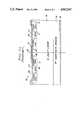
- FIG. 1Aschematically illustrates, in cross-sectional view, two cells of a prior art power MOSFET, on either side of a centerline, which includes an integral P-N junction for conducting reverse current.
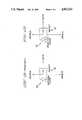
- FIG. 1Bis a schematic diagram of the equivalent circuit of the MOSFET of FIG. 1.
- FIG. 2Aschematically illustrates, in cross-sectional view, two cells of a power MOSFET with an integral Schottky barrier, on either side of a centerline, in accordance with an illustrative embodiment of the present invention.
- FIG. 2Bis a schematic diagram of the equivalent circuit of the MOSFET of FIG. 2A.
- FIG. 3schematically illustrates, in cross-sectional view, two cells of a power bipolar transistor with an integral Schottky barrier, on either side of a centerline, for accommodating reverse current.
- FIG. 1Ais a discrete vertical MOS device fabricated by planar diffusion techniques and known as a DMOS device.
- MOSFET 10 of FIG. 1Acomprises a heavily doped N + substrate 12 which serves as a drain region.
- a metallic drain electrode 16is included on the bottom surface of substrate 12.
- An epitaxially-grown N-type drift layer 14is situated on the top surface of substrate 12.
- a P-base region 18is diffused into N-drift layer 14.
- a gate electrode 20extends over the P-base region and is electrically insulated therefrom by a layer of insulation 21, so as to constitute an insulated gate electrode.
- gate electrode 20comprises a metallic layer while insulating layer 21 comprises silicon dioxide.
- a heavily doped N + source regionis diffused into P-base region 18 and contacted by a source electrode 26.
- the source regionis made up of two spaced portions 24a and 24b, enabling P-base region 18 to directly contact a source electrode 26 through a separation 27 between N + source regions 24a and 24b. This is important for establishing a fixed potential in the P-base region during device operation.
- the portion of P-base region 18 underneath gate 20defines surface channel region 28. If gate electrode 20 is externally short-circuited to source electrode 26, the carrier concentration in channel region 28 is determined by the doping level of P-base region 18. When drain electrode 16 is biased positive with respect to source electrode 26, junction J 1 between P-base region 18 and drift layer 14 is reverse biased, so that the device thus exhibits forward blocking capability.
- N + source regions 24 and N-drift region 14To carry current from drain to source (i.e., the forward conduction mode) in device 10, it is essential to form a conducting path between N + source regions 24 and N-drift region 14. This is accomplished by applying a positive bias to gate electrode 20.
- the gate biasmodulates the conductivity of channel region 28 by a strong electric field created normal to the semiconductor surface through oxide layer 21. The field strength must be sufficient to create a surface electron concentration which overcomes the concentration of P-type dopant in channel region 28.
- the resulting N-type surface layer in channel 28provides a conductive path between N + source region 24 and N-drift layer 14, resulting in current flow between drain electrode 16 and source electrode 26 through N-drift layer 14 and channel 28.
- the gate bias voltagemay be reduced to zero by externally short-circuiting gate electrode 20 to source electrode 26.
- the gate voltageis removed, electrons are no longer attracted into channel 28 and the conductive path from drain electrode 16 to source electrode 26 is broken.
- the deviceFor applications of device 10 that require a reverse current flow (i.e., from source to drain), the device includes an integral P-I-N diode-like structure which, when forward biased, conducts reverse current.
- the P-I-N diode-like structurecomprises P-base region 18, drift layer 14 and N + substrate 12. When this diode structure is forward biased, the reverse current can flow from source electrode 26 to drain electrode 16.
- FIG. 1Bis the equivalent circuit for device 10 of FIG. 1A.
- the equivalent circuitcomprises a MOSFET 30 including source, drain and gate terminals, and an integral diode 32 shown in phantom.
- the anode of diode 32is connected to the source terminal of MOSFET 30 and the cathode of the diode is connected to the drain terminal of MOSFET 30.
- junction J 1When device 10 cf FIG. 1A is in the reverse conduction mode, junction J 1 is forward biased and minority carriers are injected from P-base 18 into N-drift layer 14. Thus the integral diode in prior art power MOSFET 10 has unsatisfactory reverse recovery and forward overshoot characteristics.
- FIG. 2AA power MOSFET device 50 in accordance with an illustrative embodiment of the present invention is shown in FIG. 2A.
- the deviceincludes an integral Schottky barrier diode for conducting reverse current. Since the Schottky barrier is primarily a unipolar device and does not rely on injection of minority carriers in its conducting state, the reverse current mode of device 50 exhibits excellent reverse recovery characteristics without forward voltage overshoot.
- the structure of device 50 of FIG. 2Ais similar to the structure of device 10 of FIG. 1A except that the base region is divided into two portions so that the drift layer directly contacts the source electrode to form a Schottky barrier junction therewith.
- Power MOSFET device 50 of FIG. 2Acomprises an N + substrate 52 with a metallic drain electrode 56 included on the bottom surface of the substrate.
- An epitaxially-grown N-drift layer 54is situated on the top surface of substrate 52.
- a plurality of P-base regions 58a and 58bare diffused into the surface of drift layer 54 and are separated from each other by a distance W so that drift layer 54 can directly contact a metallic source electrode 66 and form Schottky barrier J s therewith.
- N + source regions 64a and 64bare diffused into base regions 58a and 58b respectively, and each of the source regions is in contact with source electrode 66.
- P-base regions 58a and 58bare also in contact with source electrode 66 for the reasons stated in connection with the device of FIG.
- Device 50 of FIG. 2Aincludes a gate electrode 60 which extends over P-base region 58a and is electrically insulated therefrom by an insulating layer 61, so as to constitute an insulated gate electrode.
- drift layer 54contacts the metallic source electrode and forms a Schottky barrier therewith.
- device 50 of FIG. 2Aoperates similarly to device 10 of FIG. 1A.
- gate electrode 60 and source electrode 66are externally short-circuited to each other.
- junctions J 1 between N-drift layer 54 and each of P-base regions 58a and 58bare reverse biased.
- distance Wis chosen so that in the forward blocking mode the depletion layers surrounding junctions J 1 pinch off the portion 69 of N-drift layer 54 between P-base regions 58a and 58b, suppressing leakage current from Schottky barrier J s .
- a positive voltageis applied to gate electrode 60.
- the gate-induced electric fieldattracts electrons into channel region 68 that overcomes the concentration of P-type dopant therein.
- the resulting N-type surface layer in channel 68provides a conductive path between the N + source regions and the N-drift layer.
- the integral Schottky barrier diodeis designed to have a turn-on voltage which is less than the turn-on voltage of junctions J 1 between the P-base regions and the N-drift layer.
- the turn-on voltage of the P-base/N-drift layer junctionsis about 0.7 volts.
- the Schottky barrier height for the diodein the case of a silicon device, should be chosen to be about 0.6 volts. This allows the Schottky barrier junctions to be turned on to conduct a reverse current without turning on the bipolar P-base/N-drift layer junctions. Accordingly, a reverse current can flow without minority carrier injection into the N-drift regions. This reverse current is limited by the N-drift layer resistance. Because the reverse current almost entirely comprises transport of majority carriers, the integral Schottky diode exhibits excellent reverse recovery characteristics without forward voltage overshoot transients.
- the equivalent circuit for device 50 of FIG. 2Aincludes a MOSFET 70 comprising source, gate and drain terminals and a Schottky diode 72.
- the anode of the Schottky diodeis connected to the source terminal of MOSFET 70 and the cathode is connected to the drain terminal of MOSFET 70. Therefore, the equivalent circuit of FIG. 2A is similar to that of FIG. 1A, and yet the device of FIGS. 2A and 2B does not exhibit the undesirable reverse recovery and forward voltage overshoot characteristics of the prior art device of FIGS. 1A and 1B.
- device 50 of FIG. 2Ais fabricated of silicon.
- substrate 52may have a thickness of 500 microns and a dopant concentration of 10 20 per cm 3 .
- Drift layer 54may have a thickness of 10 microns and a dopant concentration of 10 15 per cm 3 .
- P-base portions 58a and 58bmay be diffused to a depth of 2 microns and have a dopant concentration of 10 17 per cm 3 .
- Source regions 64a and 64bmay be diffused to a depth of 1 micron and have a dopant concentration of 10 20 per cm 3 .
- Distance Wmay be about 5 microns.
- the drain electrodeis comprised of nickel and the source electrode is comprised of aluminum.
- device 50has been described as being fabricated by starting with a heavily doped substrate 52 on which a less heavily doped layer 54 is epitaxially grown.
- a heavily doped substrate 52on which a less heavily doped layer 54 is epitaxially grown.
- FIG. 2Ait is also possible to fabricate devices of the type shown in FIG. 2A by starting with a wafer doped to a level corresponding to that of layer 54 and then diffusing a heavily doped region 52 on one side thereof for connection to a drain electrode.
- reverse current (as well as forward current) in device 50 of FIG. 2Ais limited by the resistance of N-drift layer 54.
- N-drift layer 54For example, a 2 amp, 2000 volt power MOSFET with an on resistance of 0.5 ohms would require an active area of 0.6 cm 2 .
- the active areais the cross-sectional area of drift layer 54 through which current flows.
- the total active areais the sum of the individual active areas of the cells.
- device 80is a vertical bipolar power transistor with an integral Schottky diode for conducting reverse current.
- the devicecomprises an N + substrate 82 with a metallic collector electrode 86 on the bottom surface of the substrate.
- An epitaxially-grown N-type conductivity collector layer 84is situated on the top surface of substrate 82.
- a P-base region 88is diffused into the top surface of N-layer 84.
- Metallic base electrodes 89are in contact with base region 88.
- An N + emitter region 94is diffused into base region 88 and is in emitter electrode 97 forms a Schottky barrier J s with collector layer 84 and is externally connected to emitter electrode 96.
- Device 80can operate in a forward blocking mode, a forward conducting mode, or a reverse conducting mode.
- junction J 2 between emitter region 94 and base region 88is not forward biased. This condition occurs, for example, if the base and emitter electrodes are short-circuited. Because junction J 2 is not forward biased, there is no minority carrier injection across junction J 2 into base region 88. If a positive voltage is now applied to collector electrode 86, junction J 1 between P-base region 88 and N-layer 84 becomes reverse biased and no current flows between collector and emitter.
- channel region 90 of layer 84 situated interiorly of, or surrounded by, P-base region 88is of width W chosen so that the region is pinched off by depletion regions surrounding the reverse-biased junction J 1 , thereby preventing flow of any leakage current through Schottky barrier J s .
- junction J 2If the emitter-base junction J 2 is now forward biased, minority carriers (i.e., electrons in this case) are injected into P-base region 88 from N + emitter 94. These minority carriers diffuse across the P-base and are collected by the reverse-biased junction J 1 . This is the so-called active gain mode of operation. If junction J 1 is not reverse biased, injection into the base will take place from both emitter region 94 and N-layer 84. In this case, the transistor is in the forward conducting mode and current flows from collector to emitter. The terminal current levels are now controlled by circuit elements external to transistor 80 of FIG. 3.
- Schottky barrier J sis used to short-circuit the collector-base-emitter structure of transistor 80.
- transistor 80operates in the reverse conduction mode when the Schottky barrier is forward biased.
- the Schottky barrieris fabricated so that it turns on at a slightly lower voltage than P-N junction J 1 .
- junction J 1turns on at about 0.7 volts so the Schottky barrier may be designed to turn on at 0.6 volts. This allows Schottky barrier J s to be forward biased without forward biasing junction J 1 . In this case, reverse current flows only through Schottky barrier J s and involves majority carriers almost exclusively.
- the Schottky barrierexhibits excellent reverse recovery characteristics without forward voltage overshoot. (Because junction J 1 is not forward biased, there is no possibility of conduction via reverse transistor action wherein collector layer 84 serves as the emitter and emitter region 94 serves as collector.)
- N + substrate 82may have a thickness of 500 microns and a dopant concentration of 10 20 per cm 3 .
- N epitaxial layer 84may have a thickness of 20 microns and a dopant concentration of 10 15 per cm 3 .
- the P-base regionmay be diffused to a depth of about 5 microns and have a dopant concentration of about 10 18 per cm 3 .
- Distance Wmay be about 5 microns.
- N + emitter region 94may be diffused to a depth on the order of 2 microns and have a dopant concentration on the order of 10 20 per cm 3 .
- Collector electrode 86may be comprised of nickel, while base electrodes 89 and emitter electrodes 96 may be comprised of aluminum.
- Emitter electrode 97 which forms the Schottky barrier with layer 84may be comprised of aluminum or tungsten.
- device 80has been described as being fabricated by starting with a heavily doped substrate on which a less heavily doped layer 84 is epitaxially grown.
- fabricated devices of the type shown in FIG. 3by starting with a wafer doped to a level corresponding to that of layer 84. Diffusion may then be used to form a heavily doped region 82 to which the collector electrode is attached.
Landscapes
- Electrodes Of Semiconductors (AREA)
Abstract
Description
Claims (7)
Priority Applications (1)
| Application Number | Priority Date | Filing Date | Title |
|---|---|---|---|
| US07/221,482US4967243A (en) | 1988-07-19 | 1988-07-19 | Power transistor structure with high speed integral antiparallel Schottky diode |
Applications Claiming Priority (1)
| Application Number | Priority Date | Filing Date | Title |
|---|---|---|---|
| US07/221,482US4967243A (en) | 1988-07-19 | 1988-07-19 | Power transistor structure with high speed integral antiparallel Schottky diode |
Publications (1)
| Publication Number | Publication Date |
|---|---|
| US4967243Atrue US4967243A (en) | 1990-10-30 |
Family
ID=22827999
Family Applications (1)
| Application Number | Title | Priority Date | Filing Date |
|---|---|---|---|
| US07/221,482Expired - LifetimeUS4967243A (en) | 1988-07-19 | 1988-07-19 | Power transistor structure with high speed integral antiparallel Schottky diode |
Country Status (1)
| Country | Link |
|---|---|
| US (1) | US4967243A (en) |
Cited By (62)
| Publication number | Priority date | Publication date | Assignee | Title |
|---|---|---|---|---|
| US5111253A (en)* | 1989-05-09 | 1992-05-05 | General Electric Company | Multicellular FET having a Schottky diode merged therewith |
| US5493134A (en)* | 1994-11-14 | 1996-02-20 | North Carolina State University | Bidirectional AC switching device with MOS-gated turn-on and turn-off control |
| FR2735617A1 (en)* | 1995-06-16 | 1996-12-20 | Sgs Thomson Microelectronics | FUNCTIONAL CELL WITH MOS TRANSISTOR AND INTEGRATED FAST DIODE |
| EP0807979A3 (en)* | 1996-05-15 | 1998-02-25 | SILICONIX Incorporated | Diode |
| US5895939A (en)* | 1995-07-20 | 1999-04-20 | Fuji Electric Co., Ltd. | Silicon carbide field effect transistor with increased avalanche withstand capability |
| US5915179A (en)* | 1995-06-09 | 1999-06-22 | Sanyo Electric Co., Ltd. | Semiconductor device and method of manufacturing the same |
| US5998836A (en)* | 1995-06-02 | 1999-12-07 | Siliconix Incorporated | Trench-gated power MOSFET with protective diode |
| US5998837A (en)* | 1995-06-02 | 1999-12-07 | Siliconix Incorporated | Trench-gated power MOSFET with protective diode having adjustable breakdown voltage |
| US6013941A (en)* | 1997-03-21 | 2000-01-11 | Oki Electric Industry Co., Ltd. | Bipolar transistor with collector surge voltage protection |
| US6049108A (en)* | 1995-06-02 | 2000-04-11 | Siliconix Incorporated | Trench-gated MOSFET with bidirectional voltage clamping |
| US6140678A (en)* | 1995-06-02 | 2000-10-31 | Siliconix Incorporated | Trench-gated power MOSFET with protective diode |
| US6163052A (en)* | 1997-04-04 | 2000-12-19 | Advanced Micro Devices, Inc. | Trench-gated vertical combination JFET and MOSFET devices |
| US6180964B1 (en)* | 1998-12-03 | 2001-01-30 | Taiwan Semiconductor Manufacturing Co., Ltd | Low leakage wire bond pad structure for integrated circuits |
| US6186408B1 (en) | 1999-05-28 | 2001-02-13 | Advanced Power Devices, Inc. | High cell density power rectifier |
| WO2001061755A1 (en)* | 2000-02-15 | 2001-08-23 | Koninklijke Philips Electronics N.V. | Semiconductor devices |
| US6331455B1 (en) | 1999-04-01 | 2001-12-18 | Advanced Power Devices, Inc. | Power rectifier device and method of fabricating power rectifier devices |
| US6537860B2 (en) | 2000-12-18 | 2003-03-25 | Apd Semiconductor, Inc. | Method of fabricating power VLSI diode devices |
| US20050247957A1 (en)* | 2004-05-07 | 2005-11-10 | Nec Electronics Corporation | Semiconductor device and method for manufacturing same |
| US20060011924A1 (en)* | 2004-07-08 | 2006-01-19 | Mazzola Michael S | Monolithic vertical junction field effect transistor and schottky barrier diode fabricated from silicon carbide and method for fabricating the same |
| US20060226478A1 (en)* | 2005-03-29 | 2006-10-12 | Brar Berinder P S | Semiconductor device having a lateral channel and contacts on opposing surfaces thereof |
| US20060226477A1 (en)* | 2005-03-29 | 2006-10-12 | Brar Berinder P S | Substrate driven field-effect transistor |
| US20060255360A1 (en)* | 2005-05-13 | 2006-11-16 | Brar Berinder P S | Semiconductor device having multiple lateral channels and method of forming the same |
| US20060273400A1 (en)* | 2005-06-01 | 2006-12-07 | Hitachi, Ltd. | High voltage analog switch ICS and ultrasound imaging systems using same |
| US20070069286A1 (en)* | 2005-09-27 | 2007-03-29 | Brar Berinder P S | Semiconductor device having an interconnect with sloped walls and method of forming the same |
| US20070187717A1 (en)* | 2005-05-13 | 2007-08-16 | Coldwatt, Inc. | Semiconductor device having reduced on-resistance and method of forming the same |
| US20070296028A1 (en)* | 2006-06-21 | 2007-12-27 | Brar Berinder P S | Vertical Field-Effect Transistor and Method of Forming the Same |
| US20070298564A1 (en)* | 2006-06-21 | 2007-12-27 | Brar Berinder P S | Vertical Field-Effect Transistor and Method of Forming the Same |
| US20070298559A1 (en)* | 2006-06-21 | 2007-12-27 | Brar Berinder P S | Vertical Field-Effect Transistor and Method of Forming the Same |
| US20080001220A1 (en)* | 2005-02-11 | 2008-01-03 | Alpha & Omega Semiconductor, Inc. | Power MOS device |
| US20080048173A1 (en)* | 2005-08-25 | 2008-02-28 | Sadaka Mariam G | Semiconductor Device Including a Lateral Field-Effect Transistor and Schottky Diode |
| US20080048174A1 (en)* | 2005-08-25 | 2008-02-28 | Sadaka Mariam G | Semiconductor Device Including a Lateral Field-Effect Transistor and Schottky Diode |
| US20080090357A1 (en)* | 2004-09-27 | 2008-04-17 | Alpha And Omega Semiconductor | Shallow source MOSFET |
| US20080164515A1 (en)* | 2007-01-08 | 2008-07-10 | Jian Li | High-density power MOSFET with planarized metalization |
| US7417266B1 (en)* | 2004-06-10 | 2008-08-26 | Qspeed Semiconductor Inc. | MOSFET having a JFET embedded as a body diode |
| US20080246081A1 (en)* | 2007-04-03 | 2008-10-09 | Vishay-Siliconix | Self-Aligned Trench MOSFET and Method of Manufacture |
| US20090065814A1 (en)* | 2005-02-11 | 2009-03-12 | Alpha & Omega Semiconductor Limited | MOS device with schottky barrier controlling layer |
| US20090065855A1 (en)* | 2005-02-11 | 2009-03-12 | Alpha & Omega Semiconductor Limited | MOS device with integrated schottky diode in active region contact trench |
| US20090065861A1 (en)* | 2005-02-11 | 2009-03-12 | Alpha & Omega Semiconductor Limited | MOS device with low injection diode |
| US20090078962A1 (en)* | 2007-09-26 | 2009-03-26 | Lakota Technologies, Inc. | Adjustable Field Effect Rectifier |
| US20110089486A1 (en)* | 2009-10-20 | 2011-04-21 | Vishay-Siliconix | Super-high density trench mosfet |
| US8421118B2 (en) | 2007-09-26 | 2013-04-16 | Stmicroelectronics N.V. | Regenerative building block and diode bridge rectifier and methods |
| US8633521B2 (en) | 2007-09-26 | 2014-01-21 | Stmicroelectronics N.V. | Self-bootstrapping field effect diode structures and methods |
| US8633094B2 (en) | 2011-12-01 | 2014-01-21 | Power Integrations, Inc. | GaN high voltage HFET with passivation plus gate dielectric multilayer structure |
| US8637368B2 (en) | 2005-02-11 | 2014-01-28 | Alpha And Omega Semiconductor Incorporated | Fabrication of MOS device with varying trench depth |
| US8643055B2 (en) | 2007-09-26 | 2014-02-04 | Stmicroelectronics N.V. | Series current limiter device |
| US8928037B2 (en) | 2013-02-28 | 2015-01-06 | Power Integrations, Inc. | Heterostructure power transistor with AlSiN passivation layer |
| US8940620B2 (en) | 2011-12-15 | 2015-01-27 | Power Integrations, Inc. | Composite wafer for fabrication of semiconductor devices |
| US20150084119A1 (en)* | 2013-09-20 | 2015-03-26 | Cree, Inc. | Layout configurations for integrating schottky contacts into a power transistor device |
| US20150084118A1 (en)* | 2013-09-20 | 2015-03-26 | Cree, Inc. | Semiconductor device including a power transistor device and bypass diode |
| US20160056148A1 (en)* | 2014-08-19 | 2016-02-25 | Fuji Electric Co., Ltd. | Semiconductor device |
| US9443974B2 (en) | 2009-08-27 | 2016-09-13 | Vishay-Siliconix | Super junction trench power MOSFET device fabrication |
| US9583482B2 (en)* | 2015-02-11 | 2017-02-28 | Monolith Semiconductor Inc. | High voltage semiconductor devices and methods of making the devices |
| US9722041B2 (en) | 2012-09-19 | 2017-08-01 | Vishay-Siliconix | Breakdown voltage blocking device |
| US9741842B2 (en) | 2013-08-08 | 2017-08-22 | Cree, Inc. | Vertical power transistor device |
| US9829387B2 (en) | 2014-10-28 | 2017-11-28 | Infineon Technologies Austria Ag | System and method for temperature sensing |
| US9882044B2 (en) | 2014-08-19 | 2018-01-30 | Vishay-Siliconix | Edge termination for super-junction MOSFETs |
| US9887259B2 (en) | 2014-06-23 | 2018-02-06 | Vishay-Siliconix | Modulated super junction power MOSFET devices |
| US10084037B2 (en) | 2007-10-05 | 2018-09-25 | Vishay-Siliconix | MOSFET active area and edge termination area charge balance |
| US10229988B2 (en) | 2012-05-30 | 2019-03-12 | Vishay-Siliconix | Adaptive charge balanced edge termination |
| US10234486B2 (en) | 2014-08-19 | 2019-03-19 | Vishay/Siliconix | Vertical sense devices in vertical trench MOSFET |
| CN110610935A (en)* | 2018-06-15 | 2019-12-24 | 英飞凌科技股份有限公司 | Power Electronics |
| US10868169B2 (en) | 2013-09-20 | 2020-12-15 | Cree, Inc. | Monolithically integrated vertical power transistor and bypass diode |
Citations (6)
| Publication number | Priority date | Publication date | Assignee | Title |
|---|---|---|---|---|
| US3391311A (en)* | 1966-02-07 | 1968-07-02 | Westinghouse Electric Corp | Constant current gain composite transistor |
| US4441117A (en)* | 1981-07-27 | 1984-04-03 | Intersil, Inc. | Monolithically merged field effect transistor and bipolar junction transistor |
| US4521795A (en)* | 1981-12-07 | 1985-06-04 | U.S. Philips Corporation | Insulated-gate field-effect transistors |
| US4605948A (en)* | 1984-08-02 | 1986-08-12 | Rca Corporation | Semiconductor structure for electric field distribution |
| US4641174A (en)* | 1983-08-08 | 1987-02-03 | General Electric Company | Pinch rectifier |
| US4783693A (en)* | 1985-07-16 | 1988-11-08 | Sgs Microelettronica Spa | Driver element for inductive loads |
- 1988
- 1988-07-19USUS07/221,482patent/US4967243A/ennot_activeExpired - Lifetime
Patent Citations (6)
| Publication number | Priority date | Publication date | Assignee | Title |
|---|---|---|---|---|
| US3391311A (en)* | 1966-02-07 | 1968-07-02 | Westinghouse Electric Corp | Constant current gain composite transistor |
| US4441117A (en)* | 1981-07-27 | 1984-04-03 | Intersil, Inc. | Monolithically merged field effect transistor and bipolar junction transistor |
| US4521795A (en)* | 1981-12-07 | 1985-06-04 | U.S. Philips Corporation | Insulated-gate field-effect transistors |
| US4641174A (en)* | 1983-08-08 | 1987-02-03 | General Electric Company | Pinch rectifier |
| US4605948A (en)* | 1984-08-02 | 1986-08-12 | Rca Corporation | Semiconductor structure for electric field distribution |
| US4783693A (en)* | 1985-07-16 | 1988-11-08 | Sgs Microelettronica Spa | Driver element for inductive loads |
Non-Patent Citations (3)
| Title |
|---|
| B. J. Baliga, Modern Power Devices, John Wiley & Sons, 1987, pp. 263 342.* |
| B. J. Baliga, Modern Power Devices, John Wiley & Sons, 1987, pp. 263-342. |
| Ser. No. 186,983, Ngo et al., 4/27/88.* |
Cited By (123)
| Publication number | Priority date | Publication date | Assignee | Title |
|---|---|---|---|---|
| US5111253A (en)* | 1989-05-09 | 1992-05-05 | General Electric Company | Multicellular FET having a Schottky diode merged therewith |
| US5493134A (en)* | 1994-11-14 | 1996-02-20 | North Carolina State University | Bidirectional AC switching device with MOS-gated turn-on and turn-off control |
| US6049108A (en)* | 1995-06-02 | 2000-04-11 | Siliconix Incorporated | Trench-gated MOSFET with bidirectional voltage clamping |
| US6140678A (en)* | 1995-06-02 | 2000-10-31 | Siliconix Incorporated | Trench-gated power MOSFET with protective diode |
| US5998836A (en)* | 1995-06-02 | 1999-12-07 | Siliconix Incorporated | Trench-gated power MOSFET with protective diode |
| US5998837A (en)* | 1995-06-02 | 1999-12-07 | Siliconix Incorporated | Trench-gated power MOSFET with protective diode having adjustable breakdown voltage |
| US5915179A (en)* | 1995-06-09 | 1999-06-22 | Sanyo Electric Co., Ltd. | Semiconductor device and method of manufacturing the same |
| FR2735617A1 (en)* | 1995-06-16 | 1996-12-20 | Sgs Thomson Microelectronics | FUNCTIONAL CELL WITH MOS TRANSISTOR AND INTEGRATED FAST DIODE |
| US5895939A (en)* | 1995-07-20 | 1999-04-20 | Fuji Electric Co., Ltd. | Silicon carbide field effect transistor with increased avalanche withstand capability |
| EP0807979A3 (en)* | 1996-05-15 | 1998-02-25 | SILICONIX Incorporated | Diode |
| US5818084A (en)* | 1996-05-15 | 1998-10-06 | Siliconix Incorporated | Pseudo-Schottky diode |
| US6476442B1 (en) | 1996-05-15 | 2002-11-05 | Siliconix Incorporated | Pseudo-Schottky diode |
| US6013941A (en)* | 1997-03-21 | 2000-01-11 | Oki Electric Industry Co., Ltd. | Bipolar transistor with collector surge voltage protection |
| US6163052A (en)* | 1997-04-04 | 2000-12-19 | Advanced Micro Devices, Inc. | Trench-gated vertical combination JFET and MOSFET devices |
| US6180964B1 (en)* | 1998-12-03 | 2001-01-30 | Taiwan Semiconductor Manufacturing Co., Ltd | Low leakage wire bond pad structure for integrated circuits |
| US6331455B1 (en) | 1999-04-01 | 2001-12-18 | Advanced Power Devices, Inc. | Power rectifier device and method of fabricating power rectifier devices |
| US6186408B1 (en) | 1999-05-28 | 2001-02-13 | Advanced Power Devices, Inc. | High cell density power rectifier |
| WO2001061755A1 (en)* | 2000-02-15 | 2001-08-23 | Koninklijke Philips Electronics N.V. | Semiconductor devices |
| US6537860B2 (en) | 2000-12-18 | 2003-03-25 | Apd Semiconductor, Inc. | Method of fabricating power VLSI diode devices |
| US20050247957A1 (en)* | 2004-05-07 | 2005-11-10 | Nec Electronics Corporation | Semiconductor device and method for manufacturing same |
| US7696061B2 (en) | 2004-05-07 | 2010-04-13 | Nec Electronics Corporation | Semiconductor device and method for manufacturing same |
| US20080032477A1 (en)* | 2004-05-07 | 2008-02-07 | Nec Electronics Corporation | Semiconductor device and method for manufacturing same |
| US7307310B2 (en)* | 2004-05-07 | 2007-12-11 | Nec Electronics Corporation | Semiconductor device and method for manufacturing same |
| US8097512B2 (en) | 2004-06-10 | 2012-01-17 | Power Integrations, Inc. | MOSFET having a JFET embedded as a body diode |
| US20080277695A1 (en)* | 2004-06-10 | 2008-11-13 | Jian Li | MOSFET Having a JFET Embedded as a Body Diode |
| US7417266B1 (en)* | 2004-06-10 | 2008-08-26 | Qspeed Semiconductor Inc. | MOSFET having a JFET embedded as a body diode |
| US20080003731A1 (en)* | 2004-07-08 | 2008-01-03 | Mazzola Michael S | Monolithic vertical junction field effect transistor and schottky barrier diode fabricated from silicon carbide and method for fabricating the same |
| US7294860B2 (en) | 2004-07-08 | 2007-11-13 | Mississippi State University | Monolithic vertical junction field effect transistor and Schottky barrier diode fabricated from silicon carbide and method for fabricating the same |
| US7416929B2 (en) | 2004-07-08 | 2008-08-26 | Semisouth Laboratories, Inc. | Monolithic vertical junction field effect transistor and schottky barrier diode fabricated from silicon carbide and method for fabricating the same |
| US20060011924A1 (en)* | 2004-07-08 | 2006-01-19 | Mazzola Michael S | Monolithic vertical junction field effect transistor and schottky barrier diode fabricated from silicon carbide and method for fabricating the same |
| US8008151B2 (en) | 2004-09-27 | 2011-08-30 | Alpha And Omega Semiconductor Limited | Shallow source MOSFET |
| US20080090357A1 (en)* | 2004-09-27 | 2008-04-17 | Alpha And Omega Semiconductor | Shallow source MOSFET |
| US7667264B2 (en) | 2004-09-27 | 2010-02-23 | Alpha And Omega Semiconductor Limited | Shallow source MOSFET |
| US8093651B2 (en) | 2005-02-11 | 2012-01-10 | Alpha & Omega Semiconductor Limited | MOS device with integrated schottky diode in active region contact trench |
| US8283723B2 (en) | 2005-02-11 | 2012-10-09 | Alpha & Omega Semiconductor Limited | MOS device with low injection diode |
| US10535764B2 (en) | 2005-02-11 | 2020-01-14 | Alpha And Omega Semiconductor Limited | Device and fabrication of MOS device with island region |
| US10978585B2 (en) | 2005-02-11 | 2021-04-13 | Alpha And Omega Semiconductor Limited | MOS device with island region |
| US20090065814A1 (en)* | 2005-02-11 | 2009-03-12 | Alpha & Omega Semiconductor Limited | MOS device with schottky barrier controlling layer |
| US7605425B2 (en) | 2005-02-11 | 2009-10-20 | Alpha & Omega Semiconductor Limited | Power MOS device |
| US20090224316A1 (en)* | 2005-02-11 | 2009-09-10 | Alpha & Omega Semiconductor, Limited | Power MOS device with conductive contact layer |
| US20080001220A1 (en)* | 2005-02-11 | 2008-01-03 | Alpha & Omega Semiconductor, Inc. | Power MOS device |
| US7800169B2 (en) | 2005-02-11 | 2010-09-21 | Alpha And Omega Semiconductor Incorporated | Power MOS device |
| US8637368B2 (en) | 2005-02-11 | 2014-01-28 | Alpha And Omega Semiconductor Incorporated | Fabrication of MOS device with varying trench depth |
| US7923774B2 (en) | 2005-02-11 | 2011-04-12 | Alpha & Omega Semiconductor Limited | Power MOS device with conductive contact layer |
| US20090065861A1 (en)* | 2005-02-11 | 2009-03-12 | Alpha & Omega Semiconductor Limited | MOS device with low injection diode |
| US8362547B2 (en) | 2005-02-11 | 2013-01-29 | Alpha & Omega Semiconductor Limited | MOS device with Schottky barrier controlling layer |
| US20090065855A1 (en)* | 2005-02-11 | 2009-03-12 | Alpha & Omega Semiconductor Limited | MOS device with integrated schottky diode in active region contact trench |
| US7439556B2 (en) | 2005-03-29 | 2008-10-21 | Coldwatt, Inc. | Substrate driven field-effect transistor |
| US20070145417A1 (en)* | 2005-03-29 | 2007-06-28 | Brar Berinder P S | High voltage semiconductor device having a lateral channel and enhanced gate-to-drain separation |
| US7439557B2 (en) | 2005-03-29 | 2008-10-21 | Coldwatt, Inc. | Semiconductor device having a lateral channel and contacts on opposing surfaces thereof |
| US20060226477A1 (en)* | 2005-03-29 | 2006-10-12 | Brar Berinder P S | Substrate driven field-effect transistor |
| US20060226478A1 (en)* | 2005-03-29 | 2006-10-12 | Brar Berinder P S | Semiconductor device having a lateral channel and contacts on opposing surfaces thereof |
| US7675090B2 (en) | 2005-05-13 | 2010-03-09 | Flextronics International Usa, Inc. | Semiconductor device having a contact on a buffer layer thereof and method of forming the same |
| US20070187717A1 (en)* | 2005-05-13 | 2007-08-16 | Coldwatt, Inc. | Semiconductor device having reduced on-resistance and method of forming the same |
| US20060255360A1 (en)* | 2005-05-13 | 2006-11-16 | Brar Berinder P S | Semiconductor device having multiple lateral channels and method of forming the same |
| US7838905B2 (en) | 2005-05-13 | 2010-11-23 | Flextronics International Usa, Inc. | Semiconductor device having multiple lateral channels and method of forming the same |
| US7339208B2 (en) | 2005-05-13 | 2008-03-04 | Coldwatt, Inc. | Semiconductor device having multiple lateral channels and method of forming the same |
| US20060273400A1 (en)* | 2005-06-01 | 2006-12-07 | Hitachi, Ltd. | High voltage analog switch ICS and ultrasound imaging systems using same |
| US7504673B2 (en) | 2005-08-25 | 2009-03-17 | Flextronics International Usa, Inc. | Semiconductor device including a lateral field-effect transistor and Schottky diode |
| US7642568B2 (en) | 2005-08-25 | 2010-01-05 | Flextronics International Usa, Inc. | Semiconductor device having substrate-driven field-effect transistor and Schottky diode and method of forming the same |
| US7655963B2 (en) | 2005-08-25 | 2010-02-02 | Flextronics International Usa, Inc. | Semiconductor device including a lateral field-effect transistor and Schottky diode |
| US20080048174A1 (en)* | 2005-08-25 | 2008-02-28 | Sadaka Mariam G | Semiconductor Device Including a Lateral Field-Effect Transistor and Schottky Diode |
| US20080048173A1 (en)* | 2005-08-25 | 2008-02-28 | Sadaka Mariam G | Semiconductor Device Including a Lateral Field-Effect Transistor and Schottky Diode |
| US20080048219A1 (en)* | 2005-08-25 | 2008-02-28 | Brar Berinder P S | Semiconductor Device Having Substrate-Driven Field-Effect Transistor and Schottky Diode and Method of Forming the Same |
| US7564074B2 (en) | 2005-08-25 | 2009-07-21 | Flextronics International Usa, Inc. | Semiconductor device including a lateral field-effect transistor and Schottky diode |
| US20080054304A1 (en)* | 2005-08-25 | 2008-03-06 | Sadaka Mariam G | Semiconductor Device Including a Lateral Field-Effect Transistor and Schottky Diode |
| US20070069286A1 (en)* | 2005-09-27 | 2007-03-29 | Brar Berinder P S | Semiconductor device having an interconnect with sloped walls and method of forming the same |
| US7462891B2 (en) | 2005-09-27 | 2008-12-09 | Coldwatt, Inc. | Semiconductor device having an interconnect with sloped walls and method of forming the same |
| US20070296028A1 (en)* | 2006-06-21 | 2007-12-27 | Brar Berinder P S | Vertical Field-Effect Transistor and Method of Forming the Same |
| US7663183B2 (en) | 2006-06-21 | 2010-02-16 | Flextronics International Usa, Inc. | Vertical field-effect transistor and method of forming the same |
| US7541640B2 (en) | 2006-06-21 | 2009-06-02 | Flextronics International Usa, Inc. | Vertical field-effect transistor and method of forming the same |
| US8415737B2 (en) | 2006-06-21 | 2013-04-09 | Flextronics International Usa, Inc. | Semiconductor device with a pillar region and method of forming the same |
| US20070298559A1 (en)* | 2006-06-21 | 2007-12-27 | Brar Berinder P S | Vertical Field-Effect Transistor and Method of Forming the Same |
| US20070298564A1 (en)* | 2006-06-21 | 2007-12-27 | Brar Berinder P S | Vertical Field-Effect Transistor and Method of Forming the Same |
| US20080164515A1 (en)* | 2007-01-08 | 2008-07-10 | Jian Li | High-density power MOSFET with planarized metalization |
| US9437729B2 (en) | 2007-01-08 | 2016-09-06 | Vishay-Siliconix | High-density power MOSFET with planarized metalization |
| US9761696B2 (en) | 2007-04-03 | 2017-09-12 | Vishay-Siliconix | Self-aligned trench MOSFET and method of manufacture |
| US20080246081A1 (en)* | 2007-04-03 | 2008-10-09 | Vishay-Siliconix | Self-Aligned Trench MOSFET and Method of Manufacture |
| US9947770B2 (en) | 2007-04-03 | 2018-04-17 | Vishay-Siliconix | Self-aligned trench MOSFET and method of manufacture |
| US8643055B2 (en) | 2007-09-26 | 2014-02-04 | Stmicroelectronics N.V. | Series current limiter device |
| US8421118B2 (en) | 2007-09-26 | 2013-04-16 | Stmicroelectronics N.V. | Regenerative building block and diode bridge rectifier and methods |
| US8148748B2 (en) | 2007-09-26 | 2012-04-03 | Stmicroelectronics N.V. | Adjustable field effect rectifier |
| US8633521B2 (en) | 2007-09-26 | 2014-01-21 | Stmicroelectronics N.V. | Self-bootstrapping field effect diode structures and methods |
| US20090078962A1 (en)* | 2007-09-26 | 2009-03-26 | Lakota Technologies, Inc. | Adjustable Field Effect Rectifier |
| US8598620B2 (en) | 2007-09-26 | 2013-12-03 | Stmicroelectronics N.V. | MOSFET with integrated field effect rectifier |
| US9048308B2 (en) | 2007-09-26 | 2015-06-02 | Stmicroelectronics International N.V. | Regenerative building block and diode bridge rectifier and methods |
| US9012954B2 (en) | 2007-09-26 | 2015-04-21 | STMicroelectronics International B.V. | Adjustable field effect rectifier |
| US9029921B2 (en) | 2007-09-26 | 2015-05-12 | Stmicroelectronics International N.V. | Self-bootstrapping field effect diode structures and methods |
| US10084037B2 (en) | 2007-10-05 | 2018-09-25 | Vishay-Siliconix | MOSFET active area and edge termination area charge balance |
| US9443974B2 (en) | 2009-08-27 | 2016-09-13 | Vishay-Siliconix | Super junction trench power MOSFET device fabrication |
| US20110089486A1 (en)* | 2009-10-20 | 2011-04-21 | Vishay-Siliconix | Super-high density trench mosfet |
| US9431530B2 (en) | 2009-10-20 | 2016-08-30 | Vishay-Siliconix | Super-high density trench MOSFET |
| US8633094B2 (en) | 2011-12-01 | 2014-01-21 | Power Integrations, Inc. | GaN high voltage HFET with passivation plus gate dielectric multilayer structure |
| US8940620B2 (en) | 2011-12-15 | 2015-01-27 | Power Integrations, Inc. | Composite wafer for fabrication of semiconductor devices |
| US10229988B2 (en) | 2012-05-30 | 2019-03-12 | Vishay-Siliconix | Adaptive charge balanced edge termination |
| US9722041B2 (en) | 2012-09-19 | 2017-08-01 | Vishay-Siliconix | Breakdown voltage blocking device |
| US8928037B2 (en) | 2013-02-28 | 2015-01-06 | Power Integrations, Inc. | Heterostructure power transistor with AlSiN passivation layer |
| USRE48380E1 (en) | 2013-08-08 | 2021-01-05 | Cree, Inc. | Vertical power transistor device |
| USRE49913E1 (en) | 2013-08-08 | 2024-04-09 | Wolfspeed, Inc. | Vertical power transistor device |
| US9741842B2 (en) | 2013-08-08 | 2017-08-22 | Cree, Inc. | Vertical power transistor device |
| US10950719B2 (en) | 2013-09-20 | 2021-03-16 | Cree, Inc. | Seminconductor device with spreading layer |
| US10868169B2 (en) | 2013-09-20 | 2020-12-15 | Cree, Inc. | Monolithically integrated vertical power transistor and bypass diode |
| US10600903B2 (en)* | 2013-09-20 | 2020-03-24 | Cree, Inc. | Semiconductor device including a power transistor device and bypass diode |
| US20150084119A1 (en)* | 2013-09-20 | 2015-03-26 | Cree, Inc. | Layout configurations for integrating schottky contacts into a power transistor device |
| US20150084118A1 (en)* | 2013-09-20 | 2015-03-26 | Cree, Inc. | Semiconductor device including a power transistor device and bypass diode |
| US9318597B2 (en)* | 2013-09-20 | 2016-04-19 | Cree, Inc. | Layout configurations for integrating schottky contacts into a power transistor device |
| US9887259B2 (en) | 2014-06-23 | 2018-02-06 | Vishay-Siliconix | Modulated super junction power MOSFET devices |
| US10283587B2 (en) | 2014-06-23 | 2019-05-07 | Vishay-Siliconix | Modulated super junction power MOSFET devices |
| US10234486B2 (en) | 2014-08-19 | 2019-03-19 | Vishay/Siliconix | Vertical sense devices in vertical trench MOSFET |
| US9882044B2 (en) | 2014-08-19 | 2018-01-30 | Vishay-Siliconix | Edge termination for super-junction MOSFETs |
| JP2016042558A (en)* | 2014-08-19 | 2016-03-31 | 富士電機株式会社 | Semiconductor device |
| US10340377B2 (en) | 2014-08-19 | 2019-07-02 | Vishay-Siliconix | Edge termination for super-junction MOSFETs |
| US10444262B2 (en) | 2014-08-19 | 2019-10-15 | Vishay-Siliconix | Vertical sense devices in vertical trench MOSFET |
| US9608072B2 (en)* | 2014-08-19 | 2017-03-28 | Fuji Electric Co., Ltd. | Semiconductor device |
| US10527654B2 (en) | 2014-08-19 | 2020-01-07 | Vishay SIliconix, LLC | Vertical sense devices in vertical trench MOSFET |
| US20160056148A1 (en)* | 2014-08-19 | 2016-02-25 | Fuji Electric Co., Ltd. | Semiconductor device |
| CN105374818B (en)* | 2014-08-19 | 2020-03-06 | 富士电机株式会社 | Semiconductor device |
| CN105374818A (en)* | 2014-08-19 | 2016-03-02 | 富士电机株式会社 | Semiconductor device |
| US9829387B2 (en) | 2014-10-28 | 2017-11-28 | Infineon Technologies Austria Ag | System and method for temperature sensing |
| US9876104B2 (en) | 2015-02-11 | 2018-01-23 | Monolith Semiconductor Inc. | High voltage semiconductor devices and methods of making the devices |
| US9583482B2 (en)* | 2015-02-11 | 2017-02-28 | Monolith Semiconductor Inc. | High voltage semiconductor devices and methods of making the devices |
| US10290732B2 (en) | 2015-02-11 | 2019-05-14 | Monolith Semiconductor Inc. | High voltage semiconductor devices and methods of making the devices |
| CN110610935A (en)* | 2018-06-15 | 2019-12-24 | 英飞凌科技股份有限公司 | Power Electronics |
Similar Documents
| Publication | Publication Date | Title |
|---|---|---|
| US4967243A (en) | Power transistor structure with high speed integral antiparallel Schottky diode | |
| US4969028A (en) | Gate enhanced rectifier | |
| US5702961A (en) | Methods of forming insulated gate bipolar transistors having built-in freewheeling diodes and transistors formed thereby | |
| US10153275B2 (en) | Method of operating an IGBT having switchable and non-switchable diode cells | |
| US4969027A (en) | Power bipolar transistor device with integral antisaturation diode | |
| US6281521B1 (en) | Silicon carbide horizontal channel buffered gate semiconductor devices | |
| US6091107A (en) | Semiconductor devices | |
| US4989058A (en) | Fast switching lateral insulated gate transistors | |
| US4646117A (en) | Power semiconductor devices with increased turn-off current ratings and limited current density in peripheral portions | |
| IE52758B1 (en) | Gate enhanced rectifier | |
| US5319222A (en) | MOS gated thyristor having on-state current saturation capability | |
| US4132996A (en) | Electric field-controlled semiconductor device | |
| EP0522670A1 (en) | Fast switching lateral insulated gate field effect transistor | |
| US4506282A (en) | Normally-off semiconductor device with low on resistance and circuit analogue | |
| CA1225164A (en) | Integrated field controlled thyristor structure with grounded cathode | |
| EP0528349A1 (en) | Insulated gate bipolar transistor having high breakdown voltage | |
| US5079607A (en) | Mos type semiconductor device | |
| US6222248B1 (en) | Electronic semiconductor power device with integrated diode | |
| EP0118007A2 (en) | Electrical circuit comprising a hybrid power switching semiconductor device including an SCR structure | |
| US5757034A (en) | Emitter switched thyristor | |
| US5455442A (en) | COMFET switch and method | |
| US4630092A (en) | Insulated gate-controlled thyristor | |
| JP7213398B2 (en) | insulated gate bipolar transistor | |
| US4309715A (en) | Integral turn-on high voltage switch | |
| US5684306A (en) | Insulated gate thyristor |
Legal Events
| Date | Code | Title | Description |
|---|---|---|---|
| AS | Assignment | Owner name:GENERAL ELECTRIC COMPANY, A NEW YORK CORP. Free format text:ASSIGNMENT OF ASSIGNORS INTEREST.;ASSIGNORS:BALIGA, BANTVAL J.;SCHLECHT, MARTIN F.;REEL/FRAME:004933/0667;SIGNING DATES FROM 19880711 TO 19880714 Owner name:GENERAL ELECTRIC COMPANY,NEW YORK Free format text:ASSIGNMENT OF ASSIGNORS INTEREST;ASSIGNORS:BALIGA, BANTVAL J.;SCHLECHT, MARTIN F.;SIGNING DATES FROM 19880711 TO 19880714;REEL/FRAME:004933/0667 | |
| FEPP | Fee payment procedure | Free format text:PAYOR NUMBER ASSIGNED (ORIGINAL EVENT CODE: ASPN); ENTITY STATUS OF PATENT OWNER: LARGE ENTITY | |
| STCF | Information on status: patent grant | Free format text:PATENTED CASE | |
| FEPP | Fee payment procedure | Free format text:PAYER NUMBER DE-ASSIGNED (ORIGINAL EVENT CODE: RMPN); ENTITY STATUS OF PATENT OWNER: LARGE ENTITY Free format text:PAYOR NUMBER ASSIGNED (ORIGINAL EVENT CODE: ASPN); ENTITY STATUS OF PATENT OWNER: LARGE ENTITY | |
| FPAY | Fee payment | Year of fee payment:4 | |
| FPAY | Fee payment | Year of fee payment:8 | |
| AS | Assignment | Owner name:INTERSIL CORPORATION, FLORIDA Free format text:ASSIGNMENT OF ASSIGNORS INTEREST;ASSIGNOR:HARRIS CORPORATION;REEL/FRAME:010255/0405 Effective date:19990813 | |
| AS | Assignment | Owner name:CREDIT SUISSE FIRST BOSTON, AS COLLATERAL AGENT, N Free format text:SECURITY INTEREST;ASSIGNOR:INTERSIL CORPORATION;REEL/FRAME:010351/0410 Effective date:19990813 | |
| AS | Assignment | Owner name:INTERSIL HOLDING CORPORATION, CALIFORNIA Free format text:INTELLECTUAL PROPERTY PARTIAL RELEASE;ASSIGNOR:CREIDT SUISSE FIRST BOSTON;REEL/FRAME:011667/0166 Effective date:20010303 | |
| AS | Assignment | Owner name:FAIRCHILD SEMICONDUCTOR CORPORATION, MAINE Free format text:REASSIGNMENT OF PATENT APPLICATIONS;ASSIGNOR:INTERSIL CORPORATION;REEL/FRAME:012002/0206 Effective date:20010406 | |
| FPAY | Fee payment | Year of fee payment:12 | |
| REMI | Maintenance fee reminder mailed |