US4967201A - Multi-layer single substrate microwave transmit/receive module - Google Patents
Multi-layer single substrate microwave transmit/receive moduleDownload PDFInfo
- Publication number
- US4967201A US4967201AUS07/111,328US11132887AUS4967201AUS 4967201 AUS4967201 AUS 4967201AUS 11132887 AUS11132887 AUS 11132887AUS 4967201 AUS4967201 AUS 4967201A
- Authority
- US
- United States
- Prior art keywords
- substrate
- module
- signal processing
- processing means
- microwave
- Prior art date
- Legal status (The legal status is an assumption and is not a legal conclusion. Google has not performed a legal analysis and makes no representation as to the accuracy of the status listed.)
- Expired - Fee Related
Links
Images


Classifications
- H—ELECTRICITY
- H01—ELECTRIC ELEMENTS
- H01L—SEMICONDUCTOR DEVICES NOT COVERED BY CLASS H10
- H01L23/00—Details of semiconductor or other solid state devices
- H01L23/58—Structural electrical arrangements for semiconductor devices not otherwise provided for, e.g. in combination with batteries
- H01L23/64—Impedance arrangements
- H01L23/66—High-frequency adaptations
- G—PHYSICS
- G01—MEASURING; TESTING
- G01S—RADIO DIRECTION-FINDING; RADIO NAVIGATION; DETERMINING DISTANCE OR VELOCITY BY USE OF RADIO WAVES; LOCATING OR PRESENCE-DETECTING BY USE OF THE REFLECTION OR RERADIATION OF RADIO WAVES; ANALOGOUS ARRANGEMENTS USING OTHER WAVES
- G01S7/00—Details of systems according to groups G01S13/00, G01S15/00, G01S17/00
- G01S7/02—Details of systems according to groups G01S13/00, G01S15/00, G01S17/00 of systems according to group G01S13/00
- G01S7/03—Details of HF subsystems specially adapted therefor, e.g. common to transmitter and receiver
- G01S7/034—Duplexers
- H—ELECTRICITY
- H01—ELECTRIC ELEMENTS
- H01L—SEMICONDUCTOR DEVICES NOT COVERED BY CLASS H10
- H01L2223/00—Details relating to semiconductor or other solid state devices covered by the group H01L23/00
- H01L2223/58—Structural electrical arrangements for semiconductor devices not otherwise provided for
- H01L2223/64—Impedance arrangements
- H01L2223/66—High-frequency adaptations
- H01L2223/6605—High-frequency electrical connections
- H01L2223/6616—Vertical connections, e.g. vias
- H01L2223/6622—Coaxial feed-throughs in active or passive substrates
- H—ELECTRICITY
- H01—ELECTRIC ELEMENTS
- H01L—SEMICONDUCTOR DEVICES NOT COVERED BY CLASS H10
- H01L2224/00—Indexing scheme for arrangements for connecting or disconnecting semiconductor or solid-state bodies and methods related thereto as covered by H01L24/00
- H01L2224/01—Means for bonding being attached to, or being formed on, the surface to be connected, e.g. chip-to-package, die-attach, "first-level" interconnects; Manufacturing methods related thereto
- H01L2224/02—Bonding areas; Manufacturing methods related thereto
- H01L2224/04—Structure, shape, material or disposition of the bonding areas prior to the connecting process
- H01L2224/05—Structure, shape, material or disposition of the bonding areas prior to the connecting process of an individual bonding area
- H01L2224/0554—External layer
- H01L2224/0555—Shape
- H01L2224/05552—Shape in top view
- H01L2224/05554—Shape in top view being square
- H—ELECTRICITY
- H01—ELECTRIC ELEMENTS
- H01L—SEMICONDUCTOR DEVICES NOT COVERED BY CLASS H10
- H01L2224/00—Indexing scheme for arrangements for connecting or disconnecting semiconductor or solid-state bodies and methods related thereto as covered by H01L24/00
- H01L2224/01—Means for bonding being attached to, or being formed on, the surface to be connected, e.g. chip-to-package, die-attach, "first-level" interconnects; Manufacturing methods related thereto
- H01L2224/42—Wire connectors; Manufacturing methods related thereto
- H01L2224/47—Structure, shape, material or disposition of the wire connectors after the connecting process
- H01L2224/48—Structure, shape, material or disposition of the wire connectors after the connecting process of an individual wire connector
- H01L2224/4805—Shape
- H01L2224/4809—Loop shape
- H01L2224/48091—Arched
- H—ELECTRICITY
- H01—ELECTRIC ELEMENTS
- H01L—SEMICONDUCTOR DEVICES NOT COVERED BY CLASS H10
- H01L2224/00—Indexing scheme for arrangements for connecting or disconnecting semiconductor or solid-state bodies and methods related thereto as covered by H01L24/00
- H01L2224/01—Means for bonding being attached to, or being formed on, the surface to be connected, e.g. chip-to-package, die-attach, "first-level" interconnects; Manufacturing methods related thereto
- H01L2224/42—Wire connectors; Manufacturing methods related thereto
- H01L2224/47—Structure, shape, material or disposition of the wire connectors after the connecting process
- H01L2224/48—Structure, shape, material or disposition of the wire connectors after the connecting process of an individual wire connector
- H01L2224/481—Disposition
- H01L2224/48151—Connecting between a semiconductor or solid-state body and an item not being a semiconductor or solid-state body, e.g. chip-to-substrate, chip-to-passive
- H01L2224/48221—Connecting between a semiconductor or solid-state body and an item not being a semiconductor or solid-state body, e.g. chip-to-substrate, chip-to-passive the body and the item being stacked
- H01L2224/48225—Connecting between a semiconductor or solid-state body and an item not being a semiconductor or solid-state body, e.g. chip-to-substrate, chip-to-passive the body and the item being stacked the item being non-metallic, e.g. insulating substrate with or without metallisation
- H01L2224/48227—Connecting between a semiconductor or solid-state body and an item not being a semiconductor or solid-state body, e.g. chip-to-substrate, chip-to-passive the body and the item being stacked the item being non-metallic, e.g. insulating substrate with or without metallisation connecting the wire to a bond pad of the item
- H—ELECTRICITY
- H01—ELECTRIC ELEMENTS
- H01L—SEMICONDUCTOR DEVICES NOT COVERED BY CLASS H10
- H01L2224/00—Indexing scheme for arrangements for connecting or disconnecting semiconductor or solid-state bodies and methods related thereto as covered by H01L24/00
- H01L2224/01—Means for bonding being attached to, or being formed on, the surface to be connected, e.g. chip-to-package, die-attach, "first-level" interconnects; Manufacturing methods related thereto
- H01L2224/42—Wire connectors; Manufacturing methods related thereto
- H01L2224/47—Structure, shape, material or disposition of the wire connectors after the connecting process
- H01L2224/49—Structure, shape, material or disposition of the wire connectors after the connecting process of a plurality of wire connectors
- H01L2224/491—Disposition
- H01L2224/4912—Layout
- H01L2224/49171—Fan-out arrangements
- H—ELECTRICITY
- H01—ELECTRIC ELEMENTS
- H01L—SEMICONDUCTOR DEVICES NOT COVERED BY CLASS H10
- H01L24/00—Arrangements for connecting or disconnecting semiconductor or solid-state bodies; Methods or apparatus related thereto
- H01L24/01—Means for bonding being attached to, or being formed on, the surface to be connected, e.g. chip-to-package, die-attach, "first-level" interconnects; Manufacturing methods related thereto
- H01L24/42—Wire connectors; Manufacturing methods related thereto
- H01L24/47—Structure, shape, material or disposition of the wire connectors after the connecting process
- H01L24/48—Structure, shape, material or disposition of the wire connectors after the connecting process of an individual wire connector
- H—ELECTRICITY
- H01—ELECTRIC ELEMENTS
- H01L—SEMICONDUCTOR DEVICES NOT COVERED BY CLASS H10
- H01L24/00—Arrangements for connecting or disconnecting semiconductor or solid-state bodies; Methods or apparatus related thereto
- H01L24/01—Means for bonding being attached to, or being formed on, the surface to be connected, e.g. chip-to-package, die-attach, "first-level" interconnects; Manufacturing methods related thereto
- H01L24/42—Wire connectors; Manufacturing methods related thereto
- H01L24/47—Structure, shape, material or disposition of the wire connectors after the connecting process
- H01L24/49—Structure, shape, material or disposition of the wire connectors after the connecting process of a plurality of wire connectors
- H—ELECTRICITY
- H01—ELECTRIC ELEMENTS
- H01L—SEMICONDUCTOR DEVICES NOT COVERED BY CLASS H10
- H01L2924/00—Indexing scheme for arrangements or methods for connecting or disconnecting semiconductor or solid-state bodies as covered by H01L24/00
- H01L2924/0001—Technical content checked by a classifier
- H01L2924/00014—Technical content checked by a classifier the subject-matter covered by the group, the symbol of which is combined with the symbol of this group, being disclosed without further technical details
- H—ELECTRICITY
- H01—ELECTRIC ELEMENTS
- H01L—SEMICONDUCTOR DEVICES NOT COVERED BY CLASS H10
- H01L2924/00—Indexing scheme for arrangements or methods for connecting or disconnecting semiconductor or solid-state bodies as covered by H01L24/00
- H01L2924/01—Chemical elements
- H01L2924/01019—Potassium [K]
- H—ELECTRICITY
- H01—ELECTRIC ELEMENTS
- H01L—SEMICONDUCTOR DEVICES NOT COVERED BY CLASS H10
- H01L2924/00—Indexing scheme for arrangements or methods for connecting or disconnecting semiconductor or solid-state bodies as covered by H01L24/00
- H01L2924/01—Chemical elements
- H01L2924/01021—Scandium [Sc]
- H—ELECTRICITY
- H01—ELECTRIC ELEMENTS
- H01L—SEMICONDUCTOR DEVICES NOT COVERED BY CLASS H10
- H01L2924/00—Indexing scheme for arrangements or methods for connecting or disconnecting semiconductor or solid-state bodies as covered by H01L24/00
- H01L2924/01—Chemical elements
- H01L2924/01039—Yttrium [Y]
- H—ELECTRICITY
- H01—ELECTRIC ELEMENTS
- H01L—SEMICONDUCTOR DEVICES NOT COVERED BY CLASS H10
- H01L2924/00—Indexing scheme for arrangements or methods for connecting or disconnecting semiconductor or solid-state bodies as covered by H01L24/00
- H01L2924/01—Chemical elements
- H01L2924/01055—Cesium [Cs]
- H—ELECTRICITY
- H01—ELECTRIC ELEMENTS
- H01L—SEMICONDUCTOR DEVICES NOT COVERED BY CLASS H10
- H01L2924/00—Indexing scheme for arrangements or methods for connecting or disconnecting semiconductor or solid-state bodies as covered by H01L24/00
- H01L2924/01—Chemical elements
- H01L2924/01068—Erbium [Er]
- H—ELECTRICITY
- H01—ELECTRIC ELEMENTS
- H01L—SEMICONDUCTOR DEVICES NOT COVERED BY CLASS H10
- H01L2924/00—Indexing scheme for arrangements or methods for connecting or disconnecting semiconductor or solid-state bodies as covered by H01L24/00
- H01L2924/01—Chemical elements
- H01L2924/01079—Gold [Au]
- H—ELECTRICITY
- H01—ELECTRIC ELEMENTS
- H01L—SEMICONDUCTOR DEVICES NOT COVERED BY CLASS H10
- H01L2924/00—Indexing scheme for arrangements or methods for connecting or disconnecting semiconductor or solid-state bodies as covered by H01L24/00
- H01L2924/095—Indexing scheme for arrangements or methods for connecting or disconnecting semiconductor or solid-state bodies as covered by H01L24/00 with a principal constituent of the material being a combination of two or more materials provided in the groups H01L2924/013 - H01L2924/0715
- H01L2924/097—Glass-ceramics, e.g. devitrified glass
- H01L2924/09701—Low temperature co-fired ceramic [LTCC]
- H—ELECTRICITY
- H01—ELECTRIC ELEMENTS
- H01L—SEMICONDUCTOR DEVICES NOT COVERED BY CLASS H10
- H01L2924/00—Indexing scheme for arrangements or methods for connecting or disconnecting semiconductor or solid-state bodies as covered by H01L24/00
- H01L2924/10—Details of semiconductor or other solid state devices to be connected
- H01L2924/11—Device type
- H01L2924/12—Passive devices, e.g. 2 terminal devices
- H01L2924/1204—Optical Diode
- H01L2924/12041—LED
- H—ELECTRICITY
- H01—ELECTRIC ELEMENTS
- H01L—SEMICONDUCTOR DEVICES NOT COVERED BY CLASS H10
- H01L2924/00—Indexing scheme for arrangements or methods for connecting or disconnecting semiconductor or solid-state bodies as covered by H01L24/00
- H01L2924/10—Details of semiconductor or other solid state devices to be connected
- H01L2924/11—Device type
- H01L2924/12—Passive devices, e.g. 2 terminal devices
- H01L2924/1204—Optical Diode
- H01L2924/12042—LASER
- H—ELECTRICITY
- H01—ELECTRIC ELEMENTS
- H01L—SEMICONDUCTOR DEVICES NOT COVERED BY CLASS H10
- H01L2924/00—Indexing scheme for arrangements or methods for connecting or disconnecting semiconductor or solid-state bodies as covered by H01L24/00
- H01L2924/10—Details of semiconductor or other solid state devices to be connected
- H01L2924/11—Device type
- H01L2924/14—Integrated circuits
- H01L2924/141—Analog devices
- H01L2924/1423—Monolithic Microwave Integrated Circuit [MMIC]
- H—ELECTRICITY
- H01—ELECTRIC ELEMENTS
- H01L—SEMICONDUCTOR DEVICES NOT COVERED BY CLASS H10
- H01L2924/00—Indexing scheme for arrangements or methods for connecting or disconnecting semiconductor or solid-state bodies as covered by H01L24/00
- H01L2924/15—Details of package parts other than the semiconductor or other solid state devices to be connected
- H01L2924/151—Die mounting substrate
- H01L2924/1515—Shape
- H01L2924/15153—Shape the die mounting substrate comprising a recess for hosting the device
- H—ELECTRICITY
- H01—ELECTRIC ELEMENTS
- H01L—SEMICONDUCTOR DEVICES NOT COVERED BY CLASS H10
- H01L2924/00—Indexing scheme for arrangements or methods for connecting or disconnecting semiconductor or solid-state bodies as covered by H01L24/00
- H01L2924/15—Details of package parts other than the semiconductor or other solid state devices to be connected
- H01L2924/151—Die mounting substrate
- H01L2924/1517—Multilayer substrate
- H—ELECTRICITY
- H01—ELECTRIC ELEMENTS
- H01L—SEMICONDUCTOR DEVICES NOT COVERED BY CLASS H10
- H01L2924/00—Indexing scheme for arrangements or methods for connecting or disconnecting semiconductor or solid-state bodies as covered by H01L24/00
- H01L2924/19—Details of hybrid assemblies other than the semiconductor or other solid state devices to be connected
- H01L2924/1901—Structure
- H01L2924/1904—Component type
- H01L2924/19041—Component type being a capacitor
- H—ELECTRICITY
- H01—ELECTRIC ELEMENTS
- H01L—SEMICONDUCTOR DEVICES NOT COVERED BY CLASS H10
- H01L2924/00—Indexing scheme for arrangements or methods for connecting or disconnecting semiconductor or solid-state bodies as covered by H01L24/00
- H01L2924/30—Technical effects
- H01L2924/301—Electrical effects
- H01L2924/3011—Impedance
Definitions
- Phased array radarsrequire many individually controllable transmit/receive modules (hereinafter T/R modules) arranged in an array of N ⁇ M modules.
- Each T/R moduleincludes microwave signal processing means comprising a number of microwave or RF frequency processing components for processing radar signals; control signal processing means comprising a number of signal processing components selectively interconnected with the microwave signal processing components for providing control signals thereto; and power conditioning means comprising a number of power conditioning components selectively interconnected with the microwave signal processing components and the control signal processing components for providing power thereto.
- microwave signal processing meanscomprising a number of microwave or RF frequency processing components for processing radar signals
- control signal processing meanscomprising a number of signal processing components selectively interconnected with the microwave signal processing components for providing control signals thereto
- power conditioning meanscomprising a number of power conditioning components selectively interconnected with the microwave signal processing components and the control signal processing components for providing power thereto.
- Phased array radarsmay require as many as 2000 T/R modules, each measuring as much as 6 inches on a side and being several inches thick and dissipating many watts of power.
- the cost of each modulemay be many thousands of dollars.
- the relatively large size of each moduleadds considerably to the cost because there are many lead connections which must be individually made and each connection (especially at microwave frequencies) must be optimally designed to reduce noise loses and side lobes.
- MMICmonolithic microwave integrated circuits
- Stockton et al.the fabrication of microwave components, whether active or passive, and their interconnections onto a single substrate has been proposed by Stockton et al. in U.S. Pat. No. 4,490,721.
- a MMIC as shown in Stockton et al.does not integrate on a substrate various functional technologies including microwave, power conditioning, control, memory and heat management.
- Stockton et al.relies on thin film techniques and IC fabrication techniques which normally have very low yields, especially when the various elements are distributed over a relatively large substrate area.
- miniaturizationis desirable because performance and cost are usually dramatically improved, the arrangement disclosed by Stockton et al. has some serious shortcomings.
- a radar trasmit/receive modulecomprising a single multi-layer substrate having at least two opposed mounting surfaces.
- the substrateincludes a plurality of integrated dielectric layers, electrical conductors and thermal conductors selectively interconnected between the layers of the substrate.
- a microwave signal processing meansis mounted on at least one of the mounting surfaces of the substrate for processing microwave radar signals.
- a control signal processing meansis mounted on at least one of the mounting surfaces of the substrate for providing control signals for the microwave signal processing means via selected electrical conductors.
- a power conditioning meansis mounted on at least one of the mounting surfaces of the substrate for providing power to the microwave signal processing means and the control signal processing means via selected electrical conductors.
- a heat sink interface means coupled to the thermal conductorsis mounted on at least one of the mounting surfaces of the substrate in thermal proximity to selected portions of the microwave signal processing means, the power conditioning means and the control signal processing means for conducting thermal energy away therefrom via selected thermal conductors.
- FIG. 1is a schematic block diagram of an illustrative embodiment of the T/R module of the present invention.
- FIG. 2is a schematic illustration, in perspective, showing the physical arrangement of the elements illustrated in FIG. 1.
- FIG. 3is a side sectional elevation of a multi-layer substrate of the present invention showing a variety of exemplary components integrated into the substrate or mounted thereon.
- FIG. 4is an illustration of an integrated component recessed into the multi-layer substrate of the present invention.
- FIG. 5Ais a partially fragmented end view of a multi-shell optical/electrical coaxial cable adapted for use in the present invention.
- FIG. 5Bis a side view of the cable taken along line 5B--5B of FIG. 5A.
- FIG. 5Cis a sectional view of the cable taken along line 5C--5C of FIG. 5A.
- FIG. 6is a schematic illustration of a T/R module similar to that shown in FIG. 1 but illustrating the individual components of the module in block form.
- FIGS. 7A-7Bare respective top and bottom views of a T/R module with the components of each functional subsystem disposed on the multi-layer substrate.
- FIG. 8is a schematic illustration of an exemplary multi-wavelength input/output optical channel.
- FIG. 1illustrates in schematic block form a T/R module 10 in accordance with the present invention.
- the module 10includes a housing 12 and a radiator R mounted therein for radiating and receiving microwave energy shown as arrows EO and ER respectively.
- the module 10further includes a single multi-layer substrate 20 (SMS 20), also shown in FIG. 2, which includes a plurality of integrated dielectric layers L, electrical conductors 22, and thermal conductors 24 selectively interconnected between the layers L.
- the substrate 20has at least two opposed mounting surfaces S1 and S2 (FIG. 2).
- a microwave signal processing means 30(sometimes hereinafter referred to as MSPM 30) is mounted on at least one of the mounting surfaces S1 for processing microwave radar signals.
- a control signal processing means 40(sometimes hereinafter referred to as CSPM 40) is mounted on at least one of the mounting surfaces S2 of the substrate 20 for providing control signals to the microwave signal processing means 30 via selected ones of the electrical conductors 22.
- a power conditioning means 50(sometimes hereinafter referred to as PCM 50) is mounted on at least one of the mounting surfaces S1 of the substrate for providing power to the microwave signal processing means 30 and the control signal processing means 40 via selected ones of the electrical conductors 22.
- a heat sink interface means 60(sometimes hereinafter referred to as HSIM 60), coupled to the thermal conductors 24, is mounted on at least one of the mounting surfaces S2 in thermal proximity to selected portions of the microwave signal processing means 30, the power conditioning means 50 and the control signal processing means for conducting thermal energy H away therefrom. Thermal energy may also be carried by selected portions of the electrical conductors 22 or by bulk energy dissipation within the substrate 20 to the heat sink interface means 60 as illustrated by the dotted arrows 24'.
- the heat sink interface means 60is in thermal contact with the housing 12 at 62 for coupling or directing thermal energy or waste heat exterior of the housing 12 as shown schematically by the enlarged wavy arrow H.
- Microwave input/output I/OMis coupled to the microwave signal processing means 30 for processing inputs and outputs thereto.
- Radiator input/output I/ORcouples the microwave signal processing means 30 with the radiator R for processing radar transmit pulses EO and radar receive pulses ER.
- Power input I/PCis coupled to the power conditioning means for providing power to the module 10.
- Control signal input I/CSis coupled to the control signal processing means 40 for providing input control signals for the T/R module 10.
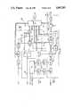
- FIG. 6is a schematic illustration of an embodiment of a T/R module 10 similar to that of FIG. 1, but shown in more detail.
- electrical control signalsare carried on electrical conductors 22C.
- Poweris carried on electrical conductors 22P and microwave energy is carried on electrical conductors (e.g. striplines) 22M.
- Thermal energyis carried on thermal conductors 24. Bulk thermal energy is conducted through the bulk of the substrate 20 and electrical conductors and is symbolically shown by the thermal conductors 24'.
- the circuit illustrated in FIG. 6includes microwave signal processing means (MSPC) 30, control signal processing means (CSPM) 40, power conditioning means (PCM) 50 and heat sink interface means (HSIM) 60.
- the MSPM 30processes microwave signals at microwave input/output I/OM via stripline electrical conductors 22M.
- the input I/OMis selectively attenuated by variable microwave attenuator MATT and selectively phase shifted by microwave phase shifter MPS which is coupled thereto.
- Transmit receive switch T/Rreceives phase shifted and attenuated microwave input signals and couples the signals to circulator CIR via drive amplifier DA and power amplifier PA.
- Radiator input/output I/OR of the circulator CIRis coupled to the radiator R which emits directed microwave or RF energy EO (shown as an arrow directed away from radiator R).
- Reflected energy signals ER(shown as an arrow directed toward radiator R) are reflected from a target (not shown), are received by the radiator R and are introduced to the receiver protector R/P via radiator input/output I/OR and circulator CIR.
- Circulator CIRis a device known in the art which allows transmitted signals to move unidirectionally therethrough and allows received signals to move unidirectionally in another direction thereby providing input and output processing over different channels, for example transmit channel XT and receive XR channel.
- the receiver protector R/Pblocks excessive reflected signal such as noise or countermeasure energy and produces an output to a two-stage low noise amplifier LNA, the output of which is coupled to the transmit receive switch T/R and to the microwave input/output I/OM via microwave phase shifter MPS and attenuator MATT.
- Microwave signals processed by the microwave signal processing means 30are carried between the various described elements by electrical conductors 22M which are illustrated as striplines. Where possible, striplines are avoided and other less complex connections are made.
- the radiator Rtransmits energy EO.
- the receive channel XR of the MSPM 30processes received energy ER from a target.
- Control for the MSPM 30is provided by control signal processing means 40 (CSPM 40).
- Control signal input I/CSdrives gate array GA through an optical coupler OC.
- Gate array GAprovides digital outputs to digital to analog converters D/A-I and D/A-II.
- the analog output of D/A-Iis coupled to operational amplifier level shifter OAS-I which provides control input for the microwave attenuator and MATT.
- the output of digital to analog converter D/A-IIis coupled to microwave phase shifter MPS through operational amplifier level shifter OAS-II.
- Gate array GAreceives a clock signal over input CLK.
- a transmit receive pulse TRP from another input control channel I/CSis coupled to transmit receive switch T/R via logic level shifter LLS to thereby control the state of the MSPM 30.
- TRP pulsealso drives logic inverter LI which has oppositely phased outputs I and II.
- Power conditioning means 50includes a regulator REG which receives input power over power input I/P and first energy storage device ES-I, and produces regulated power outputs to a pair of HEX FET switches FET-I and FET-II through second energy storage device ES-II.
- FET-Igates power to low noise amplifier LNA and FET-II gates power to power amplifier PA in response to the respective oppositely phased outputs I and II of the logic inverter LI.
- First energy storage device ES-Iis responsive to handle pulsed energy in the hundreds of microseconds range.
- Second energy storage device ES-IIis responsive to handle pulsed energy in the sub-micro second range.
- the regulator REG, FET-I and FET-II, power amplifier PA and drive amplifier DAare connected to heat sink interface means 60 (HSIM-60) via thermal conductors 24.
- Thermal conductors 24'carry heat via bulk heat transfer through the substrate 20 to conduct heat away from other elements of the system.
- the single multi-layer substrateis uniquely adapted to support, in a remarkably compact structure, all of the elements of the T/R module 10 in a rugged and reliable package less than one cubic inch in size.
- the T/R module 10is arranged so that interconnects using striplines are minimized and are often eliminated, low tolerance passive elements are utilized wherever possible, and laser trimming, often used with devices of the type described herein, is minimized.
- the single multi-layer substrate 20is formed of multiple layers L1-L8 of unfired green ceramic such as a material sold under the trademark GREENTAPE by E. I. DuPont.
- the layers L1-L8are punched with electrical vias 26 and thermal vias 28. Thereafter, various patterns of electrical conductors 22 are deposited on the layers L1-L8 and in the vias 26.
- Electrical conductors 22, referred to above with respect to FIG. 1,are generally of two types, namely, power conductors 22P and bias or control signal conductors 22C (FIG. 3).
- Electrical vias 26support electrical conductors which may carry signal and power and are referred to generally as 22V.
- Thermal vias 28are filled with thermal conductors 24. Collated layers L1-L8 are registerably laminated, trimmed, pressed and dried at low temperature and are thereafter fired at a relatively high temperature to form an integrated glass ceramic structure having electrical conductors 22 and thermal conductors 24 integrally formed therein.
- a microwave chip carrier 80(FIG. 3), formed in one embodiment of a thermally conductive base sheet 82B such as a tungsten copper matrix sold under the trade name Thermkon by Contacts Metals Welding Inc., is bonded to a gallium arsenide GaAs substrate 82S.
- the base sheet 82Bhas good thermal conductivity and has a coefficient of expansion which is close to the GaAs substrate 82S.
- the GaAs substrate 82Shas a copper layer (not shown) bonded thereto which is later etched by photolithographic techniques to form microstrip circuitry such as microwave striplines 22M, chip pads 22CP and power pads 22PP.
- Thick film capacitors C and resistors Rare usually directly formed and fired onto either or both sides S1 or S2 of the multi-layer substrate 22 or onto the chip carrier 80 if desired.
- the chip carrier 80is thereafter bonded to the substrate 20 on side S1 is illustrated.
- integrated, circuits or chips 84 and other devices which generate heat and which are also sensitive to heatare mounted on substrate 20 directly or on the chip carrier 80 at selected locations. Such locations correspond to the locations above or thermally proximate to the thermal conductors 24 so that when the individual components or the chip carrier 80 are bonded to the substrate 20 heat generating chips 84 and other elements are in thermal proximity (e.g. axially aligned) with selectively placed thermal conductors 24. Heat generated by the chips 84 is conducted through the substrate 20 from the side S1, as shown, to the side of S2.
- Heat sink interface means 60in the form of a metal film is deposited on a part of side S2 of the substrate 20 in thermal contact with the thermal conductors 24 to provide a large surface area for conveying heat H away from heat sensitive chips 84.
- a heat exchanger(not shown) may be placed in contact with HSIM 60 to remove heat from the module 10.
- Inputs and outputs of each of the chips 84are wire bonded to an electrically conducting power pads 22PP by wire bonds WB.
- a wire bond WBalso may be provided generally for input/output connections I/O.
- a totally encapsulated thick film resistor REis illustrated.
- the thick film encapsulated resistor REis formed during the part of the process in which each of the layers L1-L8 are patterned.
- Encapsulated thick film capacitorsmay be similarly formed.
- the heat pipe HPincludes an elongated chamber 90 formed partly in each of the layers L6 and L7.
- a lower end 94 of thermal conductor 24is in thermal proximity with an evaporator end 92 of the heat pipe HP.
- a working fluid (shown by the arrows WF) within the chamber 90is evaporated by heat conducted to the lower end 94 of the thermal conductor 24.
- the evaporated working fluid WFmoves to the left towards the condenser end 96 of the heat pipe HP.
- the working fluid WFcondenses on the end 104 of horizontal thermal conductor 24H, giving up its energy thereto and wicking back to the evaporator end 94 via a wick 98 as shown.
- Heat energy given up at the condenser end 96is conducted horizontally by the thermal conductor 24H to the thermal conductor 24 (to the left) which is in contact with the heat sink interface means 60 as shown.
- working fluid WFis introduced into the heat pipe HP after the substrate 20 is fired via a channel 100 which extends between the side S2 and the heat pipe HP as shown. Thereafter the channel 100 may be closed by means of the suitable ceramic plug 102 or the like.
- the chamber 90is temporarily filled with an organic material which prevents collapse of the chamber 90 as pressure is applied during the lamination process. When fired organic material burns off and leaves the chamber 90 empty for the later introduction of the working fluid WF.
- Wick 98may be formed of a suitable ceramic powder material deposited within the chamber 90 prior to firing or may be a wick line formed by a laser.
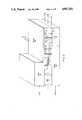
- FIGS. 7A and 7Billustrate opposite sides S1 and S2 of an exemplary embodiment of the T/R module 10 of the present invention.
- the illustrations in FIGS. 7A and 7Brepresent the layout of the various circuit elements which are shown schematically in FIGS. 1 and 6.
- the side S1 shown in FIG. 7Asupports the components forming the microwave signal processing means 30 (MSPM 30) and power conditioning means 50 (PCM 50) shown in FIGS. 1, 2 and 6.
- Side S2 shown in FIG. 7Bsupports the components forming the control signal processing means 40 (CSPM 40) and the heat sink interface means 60 (HSIM 60) in side-by-side relationship.
- CSPM 40control signal processing means 40
- HSIM 60heat sink interface means
- elements generally labeled Rare, for the most part, relatively low tolerance thick film resistors adapted for biasing various circuits in the T/R module 10. Resistor RT, however, is part of the power conditioning means PCM 50 and may be trimmed by a laser in a known manner in order to adjust or tune the resistor to a particular value.
- Elements generally labeled with the reference numeral Care energy storage capacitors which are mounted vertically (see FIG. 3). The capacitors C may be mounted to the substrate 20 at the lower end by a power pad 22PP as shown in FIG. 3. At the top end, capacitors C are connected to other elements by means of an electrical conductor 24C. A bridging connector 24B (FIG. 3) may be used to couple adjacent upper ends of the capacitors C.
- Microwave striplinesare identified by the reference numberal 22M at various locations in FIG. 7A.
- Other circuit elementsare labeled, in general, in accordance with the designations in FIG. 6 except that the microwave signal processing means 30 and power conditioning means 50 have their elements placed on the substrate 20 in the configuration shown in FIG. 7A in order to optimize the available real estate and to place the heat generating elements close to the thermal conductors 24.
- the heavy border line 80represents the shape of the chip carrier 80 which is supported by the surface S1. As mentioned earlier, the chip carrier 80 has good thermal conductivity and helps to carry heat generated by the particular elements towards the thermal conductors 24, which in turn are coupled to the heat sink interface means 60 on the opposite side S2 (FIG. 7B) of the T/R module 10.
- Optical coupler OCmay be provided for optically connecting a data stream to the module 10.
- the optical coupler OCmay include a prisim and optical sensor (described hereinafter in FIG. 8).
- heat sink interface means 60is located in thermal proximity to the thermal conductors 24 so that adequate heat exchange can occur, and so that heat generated in the power conditioning means 50 and microwave signal processing means 30 from side S1 may be conducted to the heat sink interface means 60 efficiently.
- the elements illustrated in the control signal processing means 40 in FIG. 7Bcorrespond to the elements illustrated in FIG. 6. Resistors and capacitors are respectively labeled R and C.
- a voltage reference integrated circuit VRprovides reference voltage and logic supply for the various components of CSPM 40.
- FIG. 4shows another embodiment of the present invention in which a chip 84 is mounted in a recess 120 of the substrate 20.
- a bottom wall 122 of the recess 120is formed with thermal vias 26 into which thermal conductor 24 has been deposited as hereinbefore described.
- a layer of thermally conductive material 124 and an optional layer of insulating glass or other dielectric 126Above the dielectric 126 is a power conductor 22P.
- a layer of solder or electrically conductive epoxy 128is used to attach the chip 84 to the power conductor 22P.
- An upper surface 130 of the chipis, more or less, coplanar with an upper surface 132 of the substrate 20.
- the advantage of the coplanar relationship between the upper surface 130 of the chip 84 and the upper surface 132 of the substrate 20is that the wire bonds WB may be made shorter and less susceptible to RF interference than when the chip 84 is located above the substrate surface 132.
- the distance d between the point at which the wire bond WB is attached to the top 130 of the chip 84 and the point at which it is attached to the power pads 22PP on the surface 132 of the substrate 20is less than a comparable distance d' shown in FIG. 3, for example.
- the reason for the decreased distanceis that wire bonding tools (not shown but known by those skilled in the art) used to produce wire bonds need sufficient clearance in order to clear the side wall 134 of the chip 84 when the chip is located on the substrate surface 132.
- the recessed arrangementallows for better manual or automatic alignment or fixturing during attachment of the chips 84 to the substrate 20. It is also possible to use solder preforms, which may be deposited within the recess 120, having tailored thermal and electrical impedance.
- FIG. 4illustrates that it is possible to isolate the chip 84 from the substrate 20 by means of the optional insulating glass layer 126.
- chips 84may be directly coupled without the insulating glass layer 126 to a common plane, such as, a ground plane, or to separate power planes or conductors, such as the power conductor 22P.
- chips 84may be isolated from a ground or power plane and mounted independently of each other thereby providing greater versatility to the arrangement of the present invention.
- a composite coaxial input/output cable coupler 110is provided.
- a signal carrying optical fiber OFis surrounded by a microwave conductor RF and an insulator I1.
- the cable coupler 110is coaxial with an outer grounding sheath G surrounded by an insulator I2 and a segmented coupler SC.
- An insulating cover ISsurrounds the segmented coupler SC.
- FIGS. 5A and 5Brespective end and side views of the cable coupler are shown which illustrate segmented coupler SC in detail.
- the segmented conductor SCmay be divided into conductive portions CP and insulated portions IP.
- a power conductor PCmay be located about the outer portion of the cable coupler 110, as shown, or in any other convenient location.
- Outer sheath OSsurrounds the connector 110 as shown.
- the technology development module(hereinafter TDM) exemplified in FIGS. 7A and 7B contains a representation of each function for use in evaluating performance.
- the attenuator MATT and phase shifter PS monolithic microwave integrated circuits (MMIC's) used in the TDMprovide one-third of the full attenuation and phase shift required in a full performance module.
- One voltage regulator REGis inserted into the TDM, and through this regulator passes the switched, high peak current used by the microwave signal processing means 30.
- a plurality of MMIC chips set on the chip carrier 80include power amplifier PA, drive amplifier DA, attenuator MATT, phase shifter PS, and two stage low noise amplifiers LNA using GaAs manufacturing thin film techniques.
- the alumina-glass technology developed by E.I. Dupont and sold under the trademark GREEN TAPEis used to fabricate the multilayered ceramic substrate used in the present invention.
- Each layer L1-L8(FIG. 3) is 4.5 mils thick in the green state, and the tape as a whole is flexible and punchable.
- Electrical vias 10 mils in diameter and thermal vias 25 mils inare punched in pieces blanked from a 10-inch wide roll of GREEN TAPE. All vias are backfilled with gold paste such as 5718D manufactured by DuPont.
- Conductor patternsare printed onto the green tape using off-contact screen printing procedures and material such as 5717 manufactured by DuPont. The tape with conductor patterns and filled vias is dried at 120° C. for five minutes.
- Sets of collated and registered circuit layersare placed between two sheets of mylar in a pressing die and are laminated at 70° C. and 3000 psi.
- Laminated stacksare trimmed to pre-firing size with a hot razor, steel rule die set or dicing saw.
- Burnoutoccurs at 350° C. for one hour in a convection oven, during which most of the organics are volatilized, oxidized and removed. (This prevents blistering during subsequent firing.)
- Firingis accomplished in a conventional thick film furnace for approximately two hours at a peak temperature of 850° C. for about 15 minutes. Shrinkage of approximately 12% occurs in the x and y dimensions and 17.5% in the thickness dimension.
- Top and bottom surface metalizationis screened on using material such as 5715 manufactured by DuPont and post fired. Then, thick film resistors (e.g., DuPont 1700 or 1900 series and blends thereof), additional dielectric layers (e.g., DuPont 5704), and metal layers (e.g., DuPont 9791 and 9910) are applied as needed and fired.
- thick film resistorse.g., DuPont 1700 or 1900 series and blends thereof
- additional dielectric layerse.g., DuPont 5704
- metal layerse.g., DuPont 9791 and 9910
- Thermkonis the trade name for a tungsten copper metal matrix material produced by Contact Metals Welding, Inc. It was selected for use in the TDM because it has good thermal conductivity (approximately 1.7 watts/cm-degree K) and has a coefficient of thermal expansion that very closely matches that of GaAs (6.2 ⁇ 10 -6 in/in per °C.). Since GaAs MMICs tend to be large, very thin, and extremely brittle, a difference in expansion coefficients nearly equal to 1 ⁇ 10 -6 in/in per °C. between the chip and the metal chip carrier is desirable.
- the complex shaped carrier 80(shown by the broad line 80 in FIG. 7A) for the TDM is a wire-EDMed (electron discharge machined) from a metal blank and plated.
- the 10 mil thick soft dielectric substrate material 84is punched or machined from sheet stock that has half-ounce copper rolled onto the top side.
- the punched or machined soft substrateis bonded to the thermkon carrier; then, microstrip circuitry is exposed onto the copper using photolithography.
- the carrieris etched and plated, and is then ready for MMIC chip mounting.
- the chip carrier 80is provided with its full complement of MMICs, and the miniature microwave circuit subassembly is tested.
- Other materials useful for the chip carrier 80include metal laminants or composites formed by hot isostatic pressing (HIP) techniques.
- HIPhot isostatic pressing
- nickel-clad molybdenum and copper-clad molybdenumhave been found to be useful.
- the thickness of the nickel, copper and molybdenum layersmay be tailored to adjust the coefficient of expansion so that the composite matches as closely as possible that of the gallium arsenide substrate bonded thereto.
- the nickel-clad molybdenum and copper-clad molybdenum compositesmay be punched but preferably the laminants are machined using electrochemical machining ECM.
- CM15may also be readily machined using carbide and steel tooling.
- FIG. 8illustrates schematically a useful configuration of an optical fiber OF in which multiple wavelengths L1-L2 of energy may be propagated in two directions therealong.
- the optical fiber OFcarries an input signal of the wavelength L1 which is reflected towards an optical coupler or detector D1 by means of a beam splitter BS.
- a dichroic filter DFis interposed between the detector D1 and the beam splitter BS to filter out all wavelengths except L1.
- a light emitting diode or LEDgenerates an output signal at a wavelength L2 which is coupled to the optical fiber OF through the beam splitter BS so that the optical fiber may carry two signals simultaneously.
- a receiver and filter for L2At the other end of the optical fiber (not shown), a receiver and filter for L2, a transmitter for L1 and a beam splitter are arranged in a manner similar to the arrangement shown, which should be readily apparent to those skilled in the art. Other arrangements are possible, of course, using more complex optical multiplexing techniques if desired.
Landscapes
- Engineering & Computer Science (AREA)
- Physics & Mathematics (AREA)
- General Physics & Mathematics (AREA)
- Condensed Matter Physics & Semiconductors (AREA)
- Computer Hardware Design (AREA)
- Microelectronics & Electronic Packaging (AREA)
- Power Engineering (AREA)
- Computer Networks & Wireless Communication (AREA)
- Radar, Positioning & Navigation (AREA)
- Remote Sensing (AREA)
- Waveguides (AREA)
Abstract
Description
Claims (24)
Priority Applications (1)
| Application Number | Priority Date | Filing Date | Title |
|---|---|---|---|
| US07/111,328US4967201A (en) | 1987-10-22 | 1987-10-22 | Multi-layer single substrate microwave transmit/receive module |
Applications Claiming Priority (1)
| Application Number | Priority Date | Filing Date | Title |
|---|---|---|---|
| US07/111,328US4967201A (en) | 1987-10-22 | 1987-10-22 | Multi-layer single substrate microwave transmit/receive module |
Publications (1)
| Publication Number | Publication Date |
|---|---|
| US4967201Atrue US4967201A (en) | 1990-10-30 |
Family
ID=22337872
Family Applications (1)
| Application Number | Title | Priority Date | Filing Date |
|---|---|---|---|
| US07/111,328Expired - Fee RelatedUS4967201A (en) | 1987-10-22 | 1987-10-22 | Multi-layer single substrate microwave transmit/receive module |
Country Status (1)
| Country | Link |
|---|---|
| US (1) | US4967201A (en) |
Cited By (90)
| Publication number | Priority date | Publication date | Assignee | Title |
|---|---|---|---|---|
| US5094969A (en)* | 1989-09-14 | 1992-03-10 | Litton Systems, Inc. | Method for making a stackable multilayer substrate for mounting integrated circuits |
| US5115245A (en)* | 1990-09-04 | 1992-05-19 | Hughes Aircraft Company | Single substrate microwave radar transceiver including flip-chip integrated circuits |
| US5214498A (en)* | 1990-02-26 | 1993-05-25 | Raytheon Company | MMIC package and connector |
| US5243350A (en)* | 1991-11-06 | 1993-09-07 | Grumman Aerospace Corporation | Optical control of TR modules |
| US5345205A (en)* | 1990-04-05 | 1994-09-06 | General Electric Company | Compact high density interconnected microwave system |
| US5386339A (en)* | 1993-07-29 | 1995-01-31 | Hughes Aircraft Company | Monolithic microelectronic circuit package including low-temperature-cofired-ceramic (LTCC) tape dielectric structure and in-situ heat sink |
| EP0638818A1 (en)* | 1993-08-09 | 1995-02-15 | Siemens Aktiengesellschaft | Doppler radar module using microstrip techniques |
| US5431582A (en)* | 1994-03-28 | 1995-07-11 | Raytheon Company | Module retention apparatus |
| US5457607A (en)* | 1994-03-28 | 1995-10-10 | Raytheon Company | Unified module housing |
| US5471220A (en)* | 1994-02-17 | 1995-11-28 | Itt Corporation | Integrated adaptive array antenna |
| US5493719A (en)* | 1994-07-01 | 1996-02-20 | The United States Of America As Represented By The Secretary Of The Air Force | Integrated superconductive heterodyne receiver |
| US5512901A (en)* | 1991-09-30 | 1996-04-30 | Trw Inc. | Built-in radiation structure for a millimeter wave radar sensor |
| EP0730165A3 (en)* | 1995-03-03 | 1997-01-02 | Marconi Gec Ltd | Integrated microwave circuit board for millimetric wavelengths |
| DE19535962C1 (en)* | 1995-09-27 | 1997-02-13 | Siemens Ag | Doppler radar module |
| EP0800093A1 (en)* | 1996-04-03 | 1997-10-08 | Honda Giken Kogyo Kabushiki Kaisha | Radar module and MMIC package for use in such radar module |
| WO1998026305A1 (en)* | 1996-12-10 | 1998-06-18 | Daimler-Benz Aerospace Ag | Transmitter/receiver module for a phased array radar |
| EP0741414A3 (en)* | 1995-04-27 | 1998-10-21 | Hughes Aircraft Company | Monolithic microwave integrated circuit and method |
| WO1999023717A1 (en)* | 1997-11-03 | 1999-05-14 | Raytheon Company | Digitally controlled monolithic microwave integrated circuits |
| US5940031A (en)* | 1996-09-05 | 1999-08-17 | Northrop Grumman Corporation | Transmit/receive module for planar active apertures |
| US6034633A (en)* | 1998-03-04 | 2000-03-07 | Northrop Grumman Corporation | Transmit/receive module having multiple transmit/receive paths with shared circuitry |
| US6091355A (en)* | 1998-07-21 | 2000-07-18 | Speed Products, Inc. | Doppler radar speed measuring unit |
| US6094161A (en)* | 1998-09-23 | 2000-07-25 | Northrop Grumman Corporation | Dual channel microwave transmit/receive module for an active aperture of a radar system |
| WO2000020881A3 (en)* | 1998-09-23 | 2001-05-31 | Northrop Grumman Corp | Antenna assembly including dual channel microwave transmit/receive modules |
| GB2368454A (en)* | 2000-10-24 | 2002-05-01 | Ibm | A chip carrier for a high frequency electronic device |
| US6441783B1 (en)* | 1999-10-07 | 2002-08-27 | Qinetiq Limited | Circuit module for a phased array |
| US6498551B1 (en) | 2001-08-20 | 2002-12-24 | Xytrans, Inc. | Millimeter wave module (MMW) for microwave monolithic integrated circuit (MMIC) |
| WO2003027986A1 (en)* | 2001-09-27 | 2003-04-03 | Wavetronix, Llc | Vehicular traffic sensor |
| US6545563B1 (en) | 1990-07-16 | 2003-04-08 | Raytheon Company | Digitally controlled monolithic microwave integrated circuits |
| US6594479B2 (en) | 2000-12-28 | 2003-07-15 | Lockheed Martin Corporation | Low cost MMW transceiver packaging |
| CN1118109C (en)* | 1996-06-03 | 2003-08-13 | 株式会社村田制作所 | Multi-layer thin-film electrode, high-frequency transmission line, high-frequency resonator, and high-frequency filter |
| US20040034995A1 (en)* | 2002-06-20 | 2004-02-26 | Pasi Lehtonen | Method of producing electronic unit of radio system automatically, electronic unit of radio system and electronic component used for its production |
| US20040083077A1 (en)* | 2002-10-29 | 2004-04-29 | Broadcom Corporation | Integrated packet bit error rate tester for 10G SERDES |
| US20050024166A1 (en)* | 2002-03-05 | 2005-02-03 | Xytrans, Inc. | Millimeter wave (MMW) radio frequency transceiver module and method of forming same |
| US20050094734A1 (en)* | 2003-10-29 | 2005-05-05 | Broadcom Corporation | Apparatus and method for automatic polarity swap in a communications system |
| US20050190690A1 (en)* | 2002-10-29 | 2005-09-01 | Broadcom Corporation | Multi-port, gigabit serdes transceiver capable of automatic fail switchover |
| US20050219867A1 (en)* | 2004-03-30 | 2005-10-06 | Loc Mai H | Thermal distribution system for voltage regulator |
| US20060044182A1 (en)* | 2004-08-26 | 2006-03-02 | Vacanti David C | Radar altimeter |
| WO2006039699A2 (en) | 2004-10-01 | 2006-04-13 | De Rochemont L Pierre | Ceramic antenna module and methods of manufacture thereof |
| US20070003781A1 (en)* | 2005-06-30 | 2007-01-04 | De Rochemont L P | Electrical components and method of manufacture |
| US20070015542A1 (en)* | 2005-07-18 | 2007-01-18 | Eis Electronic Integrated Systems Inc. | Antenna/transceiver configuration in a traffic sensor |
| US20070016359A1 (en)* | 2005-07-18 | 2007-01-18 | Eis Electronic Integrated Systems Inc. | Method and apparatus for providing automatic lane calibration in a traffic sensor |
| US20070030170A1 (en)* | 2005-08-05 | 2007-02-08 | Eis Electronic Integrated Systems Inc. | Processor architecture for traffic sensor and method for obtaining and processing traffic data using same |
| US20070074897A1 (en)* | 2005-09-08 | 2007-04-05 | Ronald Lashley | Thermal event detection on printed wire boards |
| DE102006004322A1 (en)* | 2006-01-31 | 2007-08-16 | Häusermann GmbH | Printed circuit board with additional functional elements as well as manufacturing process and application |
| US20070236365A1 (en)* | 2005-09-13 | 2007-10-11 | Eis Electronic Integrated Systems Inc. | Traffic sensor and method for providing a stabilized signal |
| US20070257819A1 (en)* | 2006-05-05 | 2007-11-08 | Eis Electronic Integrated Systems Inc. | Traffic sensor incorporating a video camera and method of operating same |
| US7428152B1 (en)* | 2006-10-27 | 2008-09-23 | Isothermal Systems Research, Inc. | Localized thermal management system |
| FR2936610A1 (en)* | 2008-09-30 | 2010-04-02 | Thales Sa | Hyperfrequency signal emitting and receiving module for airborne radar's active antenna, has hyperfrequency signal emission and receiving paths, switching unit and control unit with components arranged on faces of multilayered circuit |
| US20100141479A1 (en)* | 2005-10-31 | 2010-06-10 | Arnold David V | Detecting targets in roadway intersections |
| US20100149020A1 (en)* | 2005-10-31 | 2010-06-17 | Arnold David V | Detecting roadway targets across beams |
| US20100164783A1 (en)* | 2008-12-31 | 2010-07-01 | Debabani Choudhury | Platform Integrated Phased Array Transmit/Receive Module |
| US20100167666A1 (en)* | 2008-12-31 | 2010-07-01 | Debabani Choudhury | Integrated Array Transmit/Receive Module |
| US20110021007A1 (en)* | 2006-01-24 | 2011-01-27 | De Rochemont L Pierre | Liquid chemical depostion apparatus and process and products therefrom |
| US20120092218A1 (en)* | 2010-10-15 | 2012-04-19 | Fujitsu Limited | Electronic apparatus, method of making the same, and transceiving device |
| US8350657B2 (en) | 2005-06-30 | 2013-01-08 | Derochemont L Pierre | Power management module and method of manufacture |
| US8552708B2 (en) | 2010-06-02 | 2013-10-08 | L. Pierre de Rochemont | Monolithic DC/DC power management module with surface FET |
| US8699514B2 (en) | 2007-01-12 | 2014-04-15 | Broadcom Corporation | Multi-rate MAC to PHY interface |
| US8749054B2 (en) | 2010-06-24 | 2014-06-10 | L. Pierre de Rochemont | Semiconductor carrier with vertical power FET module |
| US20140160684A1 (en)* | 2012-12-06 | 2014-06-12 | Apple Inc. | Cooling for electronic components |
| US8779489B2 (en) | 2010-08-23 | 2014-07-15 | L. Pierre de Rochemont | Power FET with a resonant transistor gate |
| US8866667B2 (en) | 2012-02-22 | 2014-10-21 | Honeywell International Inc. | High sensitivity single antenna FMCW radar |
| US8922347B1 (en) | 2009-06-17 | 2014-12-30 | L. Pierre de Rochemont | R.F. energy collection circuit for wireless devices |
| US8952858B2 (en) | 2009-06-17 | 2015-02-10 | L. Pierre de Rochemont | Frequency-selective dipole antennas |
| US9023493B2 (en) | 2010-07-13 | 2015-05-05 | L. Pierre de Rochemont | Chemically complex ablative max-phase material and method of manufacture |
| US9054659B2 (en) | 2010-07-16 | 2015-06-09 | Emblation Limited | Apparatus and method for thermal interfacing |
| US9123768B2 (en) | 2010-11-03 | 2015-09-01 | L. Pierre de Rochemont | Semiconductor chip carriers with monolithically integrated quantum dot devices and method of manufacture thereof |
| US9223167B2 (en) | 2013-06-26 | 2015-12-29 | Apple Inc. | Liquid crystal switching barrier thermal control |
| US9389029B2 (en) | 2013-09-30 | 2016-07-12 | Apple Inc. | Heat transfer structure |
| US9412271B2 (en) | 2013-01-30 | 2016-08-09 | Wavetronix Llc | Traffic flow through an intersection by reducing platoon interference |
| US9660605B2 (en) | 2014-06-12 | 2017-05-23 | Honeywell International Inc. | Variable delay line using variable capacitors in a maximally flat time delay filter |
| US9674986B2 (en) | 2015-08-03 | 2017-06-06 | Apple Inc. | Parallel heat spreader |
| US10018716B2 (en) | 2014-06-26 | 2018-07-10 | Honeywell International Inc. | Systems and methods for calibration and optimization of frequency modulated continuous wave radar altimeters using adjustable self-interference cancellation |
| USD940149S1 (en) | 2017-06-08 | 2022-01-04 | Insulet Corporation | Display screen with a graphical user interface |
| USD977502S1 (en) | 2020-06-09 | 2023-02-07 | Insulet Corporation | Display screen with graphical user interface |
| US11857763B2 (en) | 2016-01-14 | 2024-01-02 | Insulet Corporation | Adjusting insulin delivery rates |
| US11865299B2 (en) | 2008-08-20 | 2024-01-09 | Insulet Corporation | Infusion pump systems and methods |
| US11929158B2 (en) | 2016-01-13 | 2024-03-12 | Insulet Corporation | User interface for diabetes management system |
| USD1020794S1 (en) | 2018-04-02 | 2024-04-02 | Bigfoot Biomedical, Inc. | Medication delivery device with icons |
| USD1024090S1 (en) | 2019-01-09 | 2024-04-23 | Bigfoot Biomedical, Inc. | Display screen or portion thereof with graphical user interface associated with insulin delivery |
| US11969579B2 (en) | 2017-01-13 | 2024-04-30 | Insulet Corporation | Insulin delivery methods, systems and devices |
| US12042630B2 (en) | 2017-01-13 | 2024-07-23 | Insulet Corporation | System and method for adjusting insulin delivery |
| US12064591B2 (en) | 2013-07-19 | 2024-08-20 | Insulet Corporation | Infusion pump system and method |
| US12076160B2 (en) | 2016-12-12 | 2024-09-03 | Insulet Corporation | Alarms and alerts for medication delivery devices and systems |
| US12097355B2 (en) | 2023-01-06 | 2024-09-24 | Insulet Corporation | Automatically or manually initiated meal bolus delivery with subsequent automatic safety constraint relaxation |
| US12106837B2 (en) | 2016-01-14 | 2024-10-01 | Insulet Corporation | Occlusion resolution in medication delivery devices, systems, and methods |
| US12301744B2 (en) | 2022-01-10 | 2025-05-13 | Apple Inc. | Handheld electronic device |
| US12318577B2 (en) | 2017-01-13 | 2025-06-03 | Insulet Corporation | System and method for adjusting insulin delivery |
| US12318594B2 (en) | 2016-05-26 | 2025-06-03 | Insulet Corporation | On-body interlock for drug delivery device |
| US12343502B2 (en) | 2017-01-13 | 2025-07-01 | Insulet Corporation | System and method for adjusting insulin delivery |
| US12383166B2 (en) | 2016-05-23 | 2025-08-12 | Insulet Corporation | Insulin delivery system and methods with risk-based set points |
Citations (11)
| Publication number | Priority date | Publication date | Assignee | Title |
|---|---|---|---|---|
| US3899720A (en)* | 1973-09-14 | 1975-08-12 | Westinghouse Electric Corp | Package for microwave integrated circuits |
| US4099318A (en)* | 1975-11-17 | 1978-07-11 | The Post Office | Semiconductor devices |
| US4251817A (en)* | 1978-10-20 | 1981-02-17 | Hitachi, Ltd. | Microwave integrated circuit device for transmission/reception of a signal |
| US4259743A (en)* | 1977-12-09 | 1981-03-31 | Hitachi, Ltd. | Transmit/receive microwave circuit |
| US4405925A (en)* | 1980-03-22 | 1983-09-20 | Licentia Patent-Verwaltungs-Gmbh | Microwave transceiver, particularly for a doppler radar system |
| US4490721A (en)* | 1980-11-17 | 1984-12-25 | Ball Corporation | Monolithic microwave integrated circuit with integral array antenna |
| US4578279A (en)* | 1981-05-26 | 1986-03-25 | International Business Machines Corporation | Inspection of multilayer ceramic circuit modules by electrical inspection of unfired green sheets |
| US4636753A (en)* | 1984-05-15 | 1987-01-13 | Communications Satellite Corporation | General technique for the integration of MIC/MMIC'S with waveguides |
| US4661836A (en)* | 1981-06-25 | 1987-04-28 | Itt Industries Inc. | Fabricating integrated circuits |
| US4729061A (en)* | 1985-04-29 | 1988-03-01 | Advanced Micro Devices, Inc. | Chip on board package for integrated circuit devices using printed circuit boards and means for conveying the heat to the opposite side of the package from the chip mounting side to permit the heat to dissipate therefrom |
| US4739334A (en)* | 1986-09-30 | 1988-04-19 | The United States Of America As Represented By The Secretary Of The Air Force | Electro-optical beamforming network for phased array antennas |
- 1987
- 1987-10-22USUS07/111,328patent/US4967201A/ennot_activeExpired - Fee Related
Patent Citations (11)
| Publication number | Priority date | Publication date | Assignee | Title |
|---|---|---|---|---|
| US3899720A (en)* | 1973-09-14 | 1975-08-12 | Westinghouse Electric Corp | Package for microwave integrated circuits |
| US4099318A (en)* | 1975-11-17 | 1978-07-11 | The Post Office | Semiconductor devices |
| US4259743A (en)* | 1977-12-09 | 1981-03-31 | Hitachi, Ltd. | Transmit/receive microwave circuit |
| US4251817A (en)* | 1978-10-20 | 1981-02-17 | Hitachi, Ltd. | Microwave integrated circuit device for transmission/reception of a signal |
| US4405925A (en)* | 1980-03-22 | 1983-09-20 | Licentia Patent-Verwaltungs-Gmbh | Microwave transceiver, particularly for a doppler radar system |
| US4490721A (en)* | 1980-11-17 | 1984-12-25 | Ball Corporation | Monolithic microwave integrated circuit with integral array antenna |
| US4578279A (en)* | 1981-05-26 | 1986-03-25 | International Business Machines Corporation | Inspection of multilayer ceramic circuit modules by electrical inspection of unfired green sheets |
| US4661836A (en)* | 1981-06-25 | 1987-04-28 | Itt Industries Inc. | Fabricating integrated circuits |
| US4636753A (en)* | 1984-05-15 | 1987-01-13 | Communications Satellite Corporation | General technique for the integration of MIC/MMIC'S with waveguides |
| US4729061A (en)* | 1985-04-29 | 1988-03-01 | Advanced Micro Devices, Inc. | Chip on board package for integrated circuit devices using printed circuit boards and means for conveying the heat to the opposite side of the package from the chip mounting side to permit the heat to dissipate therefrom |
| US4739334A (en)* | 1986-09-30 | 1988-04-19 | The United States Of America As Represented By The Secretary Of The Air Force | Electro-optical beamforming network for phased array antennas |
Non-Patent Citations (8)
| Title |
|---|
| Hori et al., GaAs Monolithic MIS s for Direct Broadcast Satellite Receivers, IEEE Transactions on Microsave Theory and Techniques, vol. MIT 31, No. 12, 12/83.* |
| Hori et al., GaAs Monolithic MIS's for Direct Broadcast Satellite Receivers, IEEE Transactions on Microsave Theory and Techniques, vol. MIT-31, No. 12, 12/83. |
| Mahle et al., MMIC s in Communications, IEEE Communications Magazine, vol. 23, No. 9, Sep. 1985.* |
| Mahle et al., MMIC's in Communications, IEEE Communications Magazine, vol. 23, No. 9, Sep. 1985. |
| Ogawa et al., A 26 GHz High Performance MIC Transmitter/Receiver for Digital Radio Subscriber Systems, IEEE Transactions on Microwave Theory and Techniques, vol. MIT 32, No. 12, Dec. 1984.* |
| Ogawa et al., A 26-GHz High-Performance MIC Transmitter/Receiver for Digital Radio Subscriber Systems, IEEE Transactions on Microwave Theory and Techniques, vol. MIT-32, No. 12, Dec. 1984. |
| Rich et al., Thermal Management Considerations for Low Temperature, Co Fireable Ceramic System, ISHM 87 Proceedings.* |
| Rich et al., Thermal Management Considerations for Low-Temperature, Co-Fireable Ceramic System, ISHM '87 Proceedings. |
Cited By (172)
| Publication number | Priority date | Publication date | Assignee | Title |
|---|---|---|---|---|
| US5094969A (en)* | 1989-09-14 | 1992-03-10 | Litton Systems, Inc. | Method for making a stackable multilayer substrate for mounting integrated circuits |
| US5214498A (en)* | 1990-02-26 | 1993-05-25 | Raytheon Company | MMIC package and connector |
| US5345205A (en)* | 1990-04-05 | 1994-09-06 | General Electric Company | Compact high density interconnected microwave system |
| US6545563B1 (en) | 1990-07-16 | 2003-04-08 | Raytheon Company | Digitally controlled monolithic microwave integrated circuits |
| US5115245A (en)* | 1990-09-04 | 1992-05-19 | Hughes Aircraft Company | Single substrate microwave radar transceiver including flip-chip integrated circuits |
| US5512901A (en)* | 1991-09-30 | 1996-04-30 | Trw Inc. | Built-in radiation structure for a millimeter wave radar sensor |
| US5243350A (en)* | 1991-11-06 | 1993-09-07 | Grumman Aerospace Corporation | Optical control of TR modules |
| US5386339A (en)* | 1993-07-29 | 1995-01-31 | Hughes Aircraft Company | Monolithic microelectronic circuit package including low-temperature-cofired-ceramic (LTCC) tape dielectric structure and in-situ heat sink |
| EP0638818A1 (en)* | 1993-08-09 | 1995-02-15 | Siemens Aktiengesellschaft | Doppler radar module using microstrip techniques |
| US5497163A (en)* | 1993-08-09 | 1996-03-05 | Siemens Aktiengesellschaft | Doppler radar module using micro-stripline technology |
| US5471220A (en)* | 1994-02-17 | 1995-11-28 | Itt Corporation | Integrated adaptive array antenna |
| US5431582A (en)* | 1994-03-28 | 1995-07-11 | Raytheon Company | Module retention apparatus |
| US5457607A (en)* | 1994-03-28 | 1995-10-10 | Raytheon Company | Unified module housing |
| US5493719A (en)* | 1994-07-01 | 1996-02-20 | The United States Of America As Represented By The Secretary Of The Air Force | Integrated superconductive heterodyne receiver |
| EP0730165A3 (en)* | 1995-03-03 | 1997-01-02 | Marconi Gec Ltd | Integrated microwave circuit board for millimetric wavelengths |
| EP0741414A3 (en)* | 1995-04-27 | 1998-10-21 | Hughes Aircraft Company | Monolithic microwave integrated circuit and method |
| DE19535962C1 (en)* | 1995-09-27 | 1997-02-13 | Siemens Ag | Doppler radar module |
| US5764189A (en)* | 1995-09-27 | 1998-06-09 | Siemens Aktiengesellschaft | Doppler radar module |
| EP0766099A3 (en)* | 1995-09-27 | 1999-05-06 | Siemens Aktiengesellschaft | Doppler radar module |
| EP0800093A1 (en)* | 1996-04-03 | 1997-10-08 | Honda Giken Kogyo Kabushiki Kaisha | Radar module and MMIC package for use in such radar module |
| CN1118109C (en)* | 1996-06-03 | 2003-08-13 | 株式会社村田制作所 | Multi-layer thin-film electrode, high-frequency transmission line, high-frequency resonator, and high-frequency filter |
| US5940031A (en)* | 1996-09-05 | 1999-08-17 | Northrop Grumman Corporation | Transmit/receive module for planar active apertures |
| WO1998026305A1 (en)* | 1996-12-10 | 1998-06-18 | Daimler-Benz Aerospace Ag | Transmitter/receiver module for a phased array radar |
| WO1999023717A1 (en)* | 1997-11-03 | 1999-05-14 | Raytheon Company | Digitally controlled monolithic microwave integrated circuits |
| EP1027751A4 (en)* | 1997-11-03 | 2008-12-03 | Raytheon Co | Digitally controlled monolithic microwave integrated circuits |
| US6034633A (en)* | 1998-03-04 | 2000-03-07 | Northrop Grumman Corporation | Transmit/receive module having multiple transmit/receive paths with shared circuitry |
| US6114986A (en)* | 1998-03-04 | 2000-09-05 | Northrop Grumman Corporation | Dual channel microwave transmit/receive module for an active aperture of a radar system |
| US6091355A (en)* | 1998-07-21 | 2000-07-18 | Speed Products, Inc. | Doppler radar speed measuring unit |
| US6094161A (en)* | 1998-09-23 | 2000-07-25 | Northrop Grumman Corporation | Dual channel microwave transmit/receive module for an active aperture of a radar system |
| WO2000022451A3 (en)* | 1998-09-23 | 2000-07-27 | Northrop Grumman Corp | A dual channel microwave transmit/receive module for an active aperture of a radar system |
| WO2000020881A3 (en)* | 1998-09-23 | 2001-05-31 | Northrop Grumman Corp | Antenna assembly including dual channel microwave transmit/receive modules |
| US6097335A (en)* | 1998-09-23 | 2000-08-01 | Northrop Grumman Corporation | Transmit/receive module having multiple transmit/receive paths with shared circuitry |
| US6441783B1 (en)* | 1999-10-07 | 2002-08-27 | Qinetiq Limited | Circuit module for a phased array |
| US6717255B2 (en) | 2000-10-24 | 2004-04-06 | International Business Machines Corporation | Chip carrier for a high-frequency electronic package |
| GB2368454B (en)* | 2000-10-24 | 2005-04-06 | Ibm | A chip carrier for high-frequency electronic device |
| GB2368454A (en)* | 2000-10-24 | 2002-05-01 | Ibm | A chip carrier for a high frequency electronic device |
| US6594479B2 (en) | 2000-12-28 | 2003-07-15 | Lockheed Martin Corporation | Low cost MMW transceiver packaging |
| US6498551B1 (en) | 2001-08-20 | 2002-12-24 | Xytrans, Inc. | Millimeter wave module (MMW) for microwave monolithic integrated circuit (MMIC) |
| US6653916B2 (en) | 2001-08-20 | 2003-11-25 | Xytrans, Inc. | Microwave monolithic integrated circuit (MMIC) carrier interface |
| US20040108922A1 (en)* | 2001-08-20 | 2004-06-10 | Xytrans, Inc. | Microwave monolithic integrated circuit (mmic) carrier interface |
| US6816041B2 (en) | 2001-08-20 | 2004-11-09 | Xytrans, Inc. | Microwave monolithic integrated circuit (MMIC) carrier interface |
| USRE48781E1 (en)* | 2001-09-27 | 2021-10-19 | Wavetronix Llc | Vehicular traffic sensor |
| WO2003027986A1 (en)* | 2001-09-27 | 2003-04-03 | Wavetronix, Llc | Vehicular traffic sensor |
| US6693557B2 (en)* | 2001-09-27 | 2004-02-17 | Wavetronix Llc | Vehicular traffic sensor |
| US20040135703A1 (en)* | 2001-09-27 | 2004-07-15 | Arnold David V. | Vehicular traffic sensor |
| US7427930B2 (en)* | 2001-09-27 | 2008-09-23 | Wavetronix Llc | Vehicular traffic sensor |
| US9735148B2 (en) | 2002-02-19 | 2017-08-15 | L. Pierre de Rochemont | Semiconductor carrier with vertical power FET module |
| US7180394B2 (en)* | 2002-03-05 | 2007-02-20 | Xytrans, Inc. | Millimeter wave (MMW) radio frequency transceiver module and method of forming same |
| US20050024166A1 (en)* | 2002-03-05 | 2005-02-03 | Xytrans, Inc. | Millimeter wave (MMW) radio frequency transceiver module and method of forming same |
| US7362562B2 (en)* | 2002-06-20 | 2008-04-22 | Nokia Corporation | Electronic unit of radio system and method of producing the same |
| US20040034995A1 (en)* | 2002-06-20 | 2004-02-26 | Pasi Lehtonen | Method of producing electronic unit of radio system automatically, electronic unit of radio system and electronic component used for its production |
| US20050190690A1 (en)* | 2002-10-29 | 2005-09-01 | Broadcom Corporation | Multi-port, gigabit serdes transceiver capable of automatic fail switchover |
| US20040117698A1 (en)* | 2002-10-29 | 2004-06-17 | Broadcom Corporation | Programmable management IO pads for an integrated circuit |
| US20060250985A1 (en)* | 2002-10-29 | 2006-11-09 | Broadcom Corporation | Multi-rate, multi-port, gigabit serdes transceiver |
| US8385188B2 (en) | 2002-10-29 | 2013-02-26 | Broadcom Corporation | Multi-port, gigabit serdes transceiver capable of automatic fail switchover |
| US8086762B2 (en) | 2002-10-29 | 2011-12-27 | Broadcom Corporation | Programmable management IO pads for an integrated circuit |
| US8023436B2 (en) | 2002-10-29 | 2011-09-20 | Broadcom Corporation | Multi-rate, multi-port, gigabit serdes transceiver |
| US8001286B2 (en) | 2002-10-29 | 2011-08-16 | Broadcom Corporation | Multipurpose and programmable pad for an integrated circuit |
| US20090252160A1 (en)* | 2002-10-29 | 2009-10-08 | Tran Hoang T | Programmable Management IO Pads for an Integrated Circuit |
| US8711677B2 (en) | 2002-10-29 | 2014-04-29 | Broadcom Corporation | Multi-port, gigabit SERDES transceiver capable of automatic fail switchover |
| US7533311B2 (en) | 2002-10-29 | 2009-05-12 | Broadcom Corporation | Programmable management IO pads for an integrated circuit |
| US7664888B2 (en) | 2002-10-29 | 2010-02-16 | Broadcom Corporation | Multipurpose and programmable pad ring for an integrated circuit |
| US9330043B2 (en) | 2002-10-29 | 2016-05-03 | Broadcom Corporation | Multi-rate, multi-port, gigabit SERDES transceiver |
| US20040083077A1 (en)* | 2002-10-29 | 2004-04-29 | Broadcom Corporation | Integrated packet bit error rate tester for 10G SERDES |
| US7355987B2 (en) | 2002-10-29 | 2008-04-08 | Broadcom Corporation | Multi-rate, multi-port, gigabit SERDES transceiver |
| US20100100651A1 (en)* | 2002-10-29 | 2010-04-22 | Broadcom Corporation | Multipurpose and programmable pad for an integrated circuit |
| US7373561B2 (en)* | 2002-10-29 | 2008-05-13 | Broadcom Corporation | Integrated packet bit error rate tester for 10G SERDES |
| US20080186987A1 (en)* | 2002-10-29 | 2008-08-07 | Broadcom Corporation | Multi-rate, muti-port, gigabit serdes transceiver |
| US20040088443A1 (en)* | 2002-10-29 | 2004-05-06 | Broadcom Corporation | Multipurpose and programmable pad ring for an integrated circuit |
| US7430240B2 (en) | 2003-10-29 | 2008-09-30 | Broadcom Corporation | Apparatus and method for automatic polarity swap in a communications system |
| US20050094734A1 (en)* | 2003-10-29 | 2005-05-05 | Broadcom Corporation | Apparatus and method for automatic polarity swap in a communications system |
| US20080304579A1 (en)* | 2003-10-29 | 2008-12-11 | Broadcom Corporation | Apparatus and method for automatic polarity swap in a communications system |
| US7630446B2 (en) | 2003-10-29 | 2009-12-08 | Broadcom Corporation | Apparatus and method for automatic polarity swap in a communications system |
| US20050219867A1 (en)* | 2004-03-30 | 2005-10-06 | Loc Mai H | Thermal distribution system for voltage regulator |
| US7239266B2 (en)* | 2004-08-26 | 2007-07-03 | Honeywell International Inc. | Radar altimeter |
| US20060044182A1 (en)* | 2004-08-26 | 2006-03-02 | Vacanti David C | Radar altimeter |
| US10673130B2 (en) | 2004-10-01 | 2020-06-02 | L. Pierre de Rochemont | Ceramic antenna module and methods of manufacture thereof |
| US9520649B2 (en) | 2004-10-01 | 2016-12-13 | L. Pierre de Rochemont | Ceramic antenna module and methods of manufacture thereof |
| US8178457B2 (en) | 2004-10-01 | 2012-05-15 | De Rochemont L Pierre | Ceramic antenna module and methods of manufacture thereof |
| EP1797617A4 (en)* | 2004-10-01 | 2009-08-12 | Rochemont L Pierre De | Ceramic antenna module and methods of manufacture thereof |
| US20090011922A1 (en)* | 2004-10-01 | 2009-01-08 | De Rochemont L Pierre | Ceramic antenna module and methods of manufacture thereof |
| US8593819B2 (en) | 2004-10-01 | 2013-11-26 | L. Pierre de Rochemont | Ceramic antenna module and methods of manufacture thereof |
| US9882274B2 (en) | 2004-10-01 | 2018-01-30 | L. Pierre de Rochemont | Ceramic antenna module and methods of manufacture thereof |
| WO2006039699A2 (en) | 2004-10-01 | 2006-04-13 | De Rochemont L Pierre | Ceramic antenna module and methods of manufacture thereof |
| US8350657B2 (en) | 2005-06-30 | 2013-01-08 | Derochemont L Pierre | Power management module and method of manufacture |
| US9905928B2 (en) | 2005-06-30 | 2018-02-27 | L. Pierre de Rochemont | Electrical components and method of manufacture |
| US8715839B2 (en) | 2005-06-30 | 2014-05-06 | L. Pierre de Rochemont | Electrical components and method of manufacture |
| US10475568B2 (en) | 2005-06-30 | 2019-11-12 | L. Pierre De Rochemont | Power management module and method of manufacture |
| US20070003781A1 (en)* | 2005-06-30 | 2007-01-04 | De Rochemont L P | Electrical components and method of manufacture |
| US20070016359A1 (en)* | 2005-07-18 | 2007-01-18 | Eis Electronic Integrated Systems Inc. | Method and apparatus for providing automatic lane calibration in a traffic sensor |
| US7454287B2 (en) | 2005-07-18 | 2008-11-18 | Image Sensing Systems, Inc. | Method and apparatus for providing automatic lane calibration in a traffic sensor |
| US7558536B2 (en) | 2005-07-18 | 2009-07-07 | EIS Electronic Integrated Systems, Inc. | Antenna/transceiver configuration in a traffic sensor |
| US20070015542A1 (en)* | 2005-07-18 | 2007-01-18 | Eis Electronic Integrated Systems Inc. | Antenna/transceiver configuration in a traffic sensor |
| US7768427B2 (en) | 2005-08-05 | 2010-08-03 | Image Sensign Systems, Inc. | Processor architecture for traffic sensor and method for obtaining and processing traffic data using same |
| US20070030170A1 (en)* | 2005-08-05 | 2007-02-08 | Eis Electronic Integrated Systems Inc. | Processor architecture for traffic sensor and method for obtaining and processing traffic data using same |
| US20070074897A1 (en)* | 2005-09-08 | 2007-04-05 | Ronald Lashley | Thermal event detection on printed wire boards |
| US7474259B2 (en) | 2005-09-13 | 2009-01-06 | Eis Electronic Integrated Systems Inc. | Traffic sensor and method for providing a stabilized signal |
| US20070236365A1 (en)* | 2005-09-13 | 2007-10-11 | Eis Electronic Integrated Systems Inc. | Traffic sensor and method for providing a stabilized signal |
| US20100141479A1 (en)* | 2005-10-31 | 2010-06-10 | Arnold David V | Detecting targets in roadway intersections |
| US9240125B2 (en) | 2005-10-31 | 2016-01-19 | Wavetronix Llc | Detecting roadway targets across beams |
| US8248272B2 (en) | 2005-10-31 | 2012-08-21 | Wavetronix | Detecting targets in roadway intersections |
| US9601014B2 (en) | 2005-10-31 | 2017-03-21 | Wavetronic Llc | Detecting roadway targets across radar beams by creating a filtered comprehensive image |
| US20100149020A1 (en)* | 2005-10-31 | 2010-06-17 | Arnold David V | Detecting roadway targets across beams |
| US10049569B2 (en) | 2005-10-31 | 2018-08-14 | Wavetronix Llc | Detecting roadway targets within a multiple beam radar system |
| US10276041B2 (en) | 2005-10-31 | 2019-04-30 | Wavetronix Llc | Detecting roadway targets across beams |
| US8665113B2 (en) | 2005-10-31 | 2014-03-04 | Wavetronix Llc | Detecting roadway targets across beams including filtering computed positions |
| US8354294B2 (en) | 2006-01-24 | 2013-01-15 | De Rochemont L Pierre | Liquid chemical deposition apparatus and process and products therefrom |
| US20110021007A1 (en)* | 2006-01-24 | 2011-01-27 | De Rochemont L Pierre | Liquid chemical depostion apparatus and process and products therefrom |
| US8715814B2 (en) | 2006-01-24 | 2014-05-06 | L. Pierre de Rochemont | Liquid chemical deposition apparatus and process and products therefrom |
| DE102006004322A1 (en)* | 2006-01-31 | 2007-08-16 | Häusermann GmbH | Printed circuit board with additional functional elements as well as manufacturing process and application |
| US20090314522A1 (en)* | 2006-01-31 | 2009-12-24 | Rudolf Janesch | Printed Circuit Board With Additional Functional Elements, Method of Production and Use |
| US7541943B2 (en) | 2006-05-05 | 2009-06-02 | Eis Electronic Integrated Systems Inc. | Traffic sensor incorporating a video camera and method of operating same |
| US20070257819A1 (en)* | 2006-05-05 | 2007-11-08 | Eis Electronic Integrated Systems Inc. | Traffic sensor incorporating a video camera and method of operating same |
| US7428152B1 (en)* | 2006-10-27 | 2008-09-23 | Isothermal Systems Research, Inc. | Localized thermal management system |
| US8699514B2 (en) | 2007-01-12 | 2014-04-15 | Broadcom Corporation | Multi-rate MAC to PHY interface |
| US9379988B2 (en) | 2007-01-12 | 2016-06-28 | Broadcom Corporation | Multi-rate MAC to PHY interface |
| US12296139B2 (en) | 2008-08-20 | 2025-05-13 | Insulet Corporation | Infusion pump systems and methods |
| US11865299B2 (en) | 2008-08-20 | 2024-01-09 | Insulet Corporation | Infusion pump systems and methods |
| FR2936610A1 (en)* | 2008-09-30 | 2010-04-02 | Thales Sa | Hyperfrequency signal emitting and receiving module for airborne radar's active antenna, has hyperfrequency signal emission and receiving paths, switching unit and control unit with components arranged on faces of multilayered circuit |
| US20100164783A1 (en)* | 2008-12-31 | 2010-07-01 | Debabani Choudhury | Platform Integrated Phased Array Transmit/Receive Module |
| WO2010078199A3 (en)* | 2008-12-31 | 2010-10-14 | Intel Corporation | Integrated array transmit/receive module |
| US8467737B2 (en) | 2008-12-31 | 2013-06-18 | Intel Corporation | Integrated array transmit/receive module |
| US8706049B2 (en) | 2008-12-31 | 2014-04-22 | Intel Corporation | Platform integrated phased array transmit/receive module |
| US20100167666A1 (en)* | 2008-12-31 | 2010-07-01 | Debabani Choudhury | Integrated Array Transmit/Receive Module |
| TWI396393B (en)* | 2008-12-31 | 2013-05-11 | Intel Corp | Apparatus for transmitting/receiving signals |
| JP2012514426A (en)* | 2008-12-31 | 2012-06-21 | インテル コーポレイション | Integrated array transceiver module |
| US11063365B2 (en) | 2009-06-17 | 2021-07-13 | L. Pierre de Rochemont | Frequency-selective dipole antennas |
| US8922347B1 (en) | 2009-06-17 | 2014-12-30 | L. Pierre de Rochemont | R.F. energy collection circuit for wireless devices |
| US8952858B2 (en) | 2009-06-17 | 2015-02-10 | L. Pierre de Rochemont | Frequency-selective dipole antennas |
| US9893564B2 (en) | 2009-06-17 | 2018-02-13 | L. Pierre de Rochemont | R.F. energy collection circuit for wireless devices |
| US9847581B2 (en) | 2009-06-17 | 2017-12-19 | L. Pierre de Rochemont | Frequency-selective dipole antennas |
| US8552708B2 (en) | 2010-06-02 | 2013-10-08 | L. Pierre de Rochemont | Monolithic DC/DC power management module with surface FET |
| US10483260B2 (en) | 2010-06-24 | 2019-11-19 | L. Pierre de Rochemont | Semiconductor carrier with vertical power FET module |
| US8749054B2 (en) | 2010-06-24 | 2014-06-10 | L. Pierre de Rochemont | Semiconductor carrier with vertical power FET module |
| US10683705B2 (en) | 2010-07-13 | 2020-06-16 | L. Pierre de Rochemont | Cutting tool and method of manufacture |
| US9023493B2 (en) | 2010-07-13 | 2015-05-05 | L. Pierre de Rochemont | Chemically complex ablative max-phase material and method of manufacture |
| US9054659B2 (en) | 2010-07-16 | 2015-06-09 | Emblation Limited | Apparatus and method for thermal interfacing |
| US8779489B2 (en) | 2010-08-23 | 2014-07-15 | L. Pierre de Rochemont | Power FET with a resonant transistor gate |
| US20120092218A1 (en)* | 2010-10-15 | 2012-04-19 | Fujitsu Limited | Electronic apparatus, method of making the same, and transceiving device |
| CN102456639A (en)* | 2010-10-15 | 2012-05-16 | 富士通株式会社 | Electronic apparatus, method of making the same, and transceiving device |
| US8952846B2 (en)* | 2010-10-15 | 2015-02-10 | Fujitsu Limited | Electronic apparatus, method of making the same, and transceiving device |
| US10777409B2 (en) | 2010-11-03 | 2020-09-15 | L. Pierre de Rochemont | Semiconductor chip carriers with monolithically integrated quantum dot devices and method of manufacture thereof |
| US9123768B2 (en) | 2010-11-03 | 2015-09-01 | L. Pierre de Rochemont | Semiconductor chip carriers with monolithically integrated quantum dot devices and method of manufacture thereof |
| US8866667B2 (en) | 2012-02-22 | 2014-10-21 | Honeywell International Inc. | High sensitivity single antenna FMCW radar |
| US9125299B2 (en)* | 2012-12-06 | 2015-09-01 | Apple Inc. | Cooling for electronic components |
| US20140160684A1 (en)* | 2012-12-06 | 2014-06-12 | Apple Inc. | Cooling for electronic components |
| US9412271B2 (en) | 2013-01-30 | 2016-08-09 | Wavetronix Llc | Traffic flow through an intersection by reducing platoon interference |
| US9223167B2 (en) | 2013-06-26 | 2015-12-29 | Apple Inc. | Liquid crystal switching barrier thermal control |
| US12064591B2 (en) | 2013-07-19 | 2024-08-20 | Insulet Corporation | Infusion pump system and method |
| US9389029B2 (en) | 2013-09-30 | 2016-07-12 | Apple Inc. | Heat transfer structure |
| US9660605B2 (en) | 2014-06-12 | 2017-05-23 | Honeywell International Inc. | Variable delay line using variable capacitors in a maximally flat time delay filter |
| US10018716B2 (en) | 2014-06-26 | 2018-07-10 | Honeywell International Inc. | Systems and methods for calibration and optimization of frequency modulated continuous wave radar altimeters using adjustable self-interference cancellation |
| US9674986B2 (en) | 2015-08-03 | 2017-06-06 | Apple Inc. | Parallel heat spreader |
| US11929158B2 (en) | 2016-01-13 | 2024-03-12 | Insulet Corporation | User interface for diabetes management system |
| US12303667B2 (en) | 2016-01-14 | 2025-05-20 | Insulet Corporation | Adjusting insulin delivery rates |
| US12303668B2 (en) | 2016-01-14 | 2025-05-20 | Insulet Corporation | Adjusting insulin delivery rates |
| US11857763B2 (en) | 2016-01-14 | 2024-01-02 | Insulet Corporation | Adjusting insulin delivery rates |
| US12106837B2 (en) | 2016-01-14 | 2024-10-01 | Insulet Corporation | Occlusion resolution in medication delivery devices, systems, and methods |
| US12383166B2 (en) | 2016-05-23 | 2025-08-12 | Insulet Corporation | Insulin delivery system and methods with risk-based set points |
| US12318594B2 (en) | 2016-05-26 | 2025-06-03 | Insulet Corporation | On-body interlock for drug delivery device |
| US12076160B2 (en) | 2016-12-12 | 2024-09-03 | Insulet Corporation | Alarms and alerts for medication delivery devices and systems |
| US12042630B2 (en) | 2017-01-13 | 2024-07-23 | Insulet Corporation | System and method for adjusting insulin delivery |
| US12343502B2 (en) | 2017-01-13 | 2025-07-01 | Insulet Corporation | System and method for adjusting insulin delivery |
| US12161841B2 (en) | 2017-01-13 | 2024-12-10 | Insulet Corporation | Insulin delivery methods, systems and devices |
| US11969579B2 (en) | 2017-01-13 | 2024-04-30 | Insulet Corporation | Insulin delivery methods, systems and devices |
| US12318577B2 (en) | 2017-01-13 | 2025-06-03 | Insulet Corporation | System and method for adjusting insulin delivery |
| USD940149S1 (en) | 2017-06-08 | 2022-01-04 | Insulet Corporation | Display screen with a graphical user interface |
| USD1020794S1 (en) | 2018-04-02 | 2024-04-02 | Bigfoot Biomedical, Inc. | Medication delivery device with icons |
| USD1024090S1 (en) | 2019-01-09 | 2024-04-23 | Bigfoot Biomedical, Inc. | Display screen or portion thereof with graphical user interface associated with insulin delivery |
| USD977502S1 (en) | 2020-06-09 | 2023-02-07 | Insulet Corporation | Display screen with graphical user interface |
| US12301744B2 (en) | 2022-01-10 | 2025-05-13 | Apple Inc. | Handheld electronic device |
| US12097355B2 (en) | 2023-01-06 | 2024-09-24 | Insulet Corporation | Automatically or manually initiated meal bolus delivery with subsequent automatic safety constraint relaxation |
Similar Documents
| Publication | Publication Date | Title |
|---|---|---|
| US4967201A (en) | Multi-layer single substrate microwave transmit/receive module | |
| US6249439B1 (en) | Millimeter wave multilayer assembly | |
| US6324755B1 (en) | Solid interface module | |
| US6998708B2 (en) | Millimeter wave (MMW) transceiver module with transmitter, receiver and local oscillator frequency multiplier surface mounted chip set | |
| US5768109A (en) | Multi-layer circuit board and semiconductor flip chip connection | |
| US6788171B2 (en) | Millimeter wave (MMW) radio frequency transceiver module and method of forming same | |
| US5019829A (en) | Plug-in package for microwave integrated circuit having cover-mounted antenna | |
| US6580402B2 (en) | Antenna integrated ceramic chip carrier for a phased array antenna | |
| US20040080917A1 (en) | Integrated microwave package and the process for making the same | |
| US5132648A (en) | Large array MMIC feedthrough | |
| US5757074A (en) | Microwave/millimeter wave circuit structure with discrete flip-chip mounted elements | |
| US6175287B1 (en) | Direct backside interconnect for multiple chip assemblies | |
| EP1211730B1 (en) | Stacked power amplifier module | |
| EP1186033B1 (en) | Carrier for electronic components and a method for manufacturing a carrier | |
| US6594479B2 (en) | Low cost MMW transceiver packaging | |
| US5717249A (en) | RF power amplifying circuit device | |
| US5559363A (en) | Off-chip impedance matching utilizing a dielectric element and high density interconnect technology | |
| US5338975A (en) | High density interconnect structure including a spacer structure and a gap | |
| US5451818A (en) | Millimeter wave ceramic package | |
| WO1988006351A1 (en) | A transmit-receive means for phased-array active antenna system | |
| KR20080018248A (en) | Reduced inductance interconnects for advanced microwave and millimeter wave systems | |
| EP0412528A2 (en) | Electronic circuit package and production thereof | |
| EP1976350B1 (en) | Method and structure for RF antenna module | |
| US6198456B1 (en) | Integrated transmitter or receiver device | |
| GB2189084A (en) | Integrated circuit packaging |
Legal Events
| Date | Code | Title | Description |
|---|---|---|---|
| AS | Assignment | Owner name:WESTINGHOUSE ELECTRIC CORPORATION, WESTINGHOUSE BL Free format text:ASSIGNMENT OF ASSIGNORS INTEREST.;ASSIGNOR:RICH, EDWARD L. III;REEL/FRAME:004842/0457 Effective date:19880118 Owner name:WESTINGHOUSE ELECTRIC CORPORATION, A CORP. OF PA,P Free format text:ASSIGNMENT OF ASSIGNORS INTEREST;ASSIGNOR:RICH, EDWARD L. III;REEL/FRAME:004842/0457 Effective date:19880118 | |
| FEPP | Fee payment procedure | Free format text:PAYOR NUMBER ASSIGNED (ORIGINAL EVENT CODE: ASPN); ENTITY STATUS OF PATENT OWNER: LARGE ENTITY | |
| FPAY | Fee payment | Year of fee payment:4 | |
| AS | Assignment | Owner name:NORTHROP GRUMMAN CORPORATION, CALIFORNIA Free format text:ASSIGNMENT OF ASSIGNORS INTEREST;ASSIGNOR:WESTINGHOUSE ELECTRIC CORPORATION;REEL/FRAME:008104/0190 Effective date:19960301 | |
| FEPP | Fee payment procedure | Free format text:PAYOR NUMBER ASSIGNED (ORIGINAL EVENT CODE: ASPN); ENTITY STATUS OF PATENT OWNER: LARGE ENTITY Free format text:PAYER NUMBER DE-ASSIGNED (ORIGINAL EVENT CODE: RMPN); ENTITY STATUS OF PATENT OWNER: LARGE ENTITY | |
| REMI | Maintenance fee reminder mailed | ||
| LAPS | Lapse for failure to pay maintenance fees | ||
| FP | Lapsed due to failure to pay maintenance fee | Effective date:19981030 | |
| STCH | Information on status: patent discontinuation | Free format text:PATENT EXPIRED DUE TO NONPAYMENT OF MAINTENANCE FEES UNDER 37 CFR 1.362 |