US4966885A - Method of producing a device comprising a metal oxide superconductor layer - Google Patents
Method of producing a device comprising a metal oxide superconductor layerDownload PDFInfo
- Publication number
- US4966885A US4966885AUS07/398,797US39879789AUS4966885AUS 4966885 AUS4966885 AUS 4966885AUS 39879789 AUS39879789 AUS 39879789AUS 4966885 AUS4966885 AUS 4966885A
- Authority
- US
- United States
- Prior art keywords
- film
- superconductor
- metal oxide
- layer
- thinning
- Prior art date
- Legal status (The legal status is an assumption and is not a legal conclusion. Google has not performed a legal analysis and makes no representation as to the accuracy of the status listed.)
- Expired - Lifetime
Links
Images

Classifications
- H—ELECTRICITY
- H10—SEMICONDUCTOR DEVICES; ELECTRIC SOLID-STATE DEVICES NOT OTHERWISE PROVIDED FOR
- H10N—ELECTRIC SOLID-STATE DEVICES NOT OTHERWISE PROVIDED FOR
- H10N60/00—Superconducting devices
- H10N60/01—Manufacture or treatment
- H10N60/0268—Manufacture or treatment of devices comprising copper oxide
- H10N60/0661—Processes performed after copper oxide formation, e.g. patterning
- H10N60/0688—Etching
- Y—GENERAL TAGGING OF NEW TECHNOLOGICAL DEVELOPMENTS; GENERAL TAGGING OF CROSS-SECTIONAL TECHNOLOGIES SPANNING OVER SEVERAL SECTIONS OF THE IPC; TECHNICAL SUBJECTS COVERED BY FORMER USPC CROSS-REFERENCE ART COLLECTIONS [XRACs] AND DIGESTS
- Y10—TECHNICAL SUBJECTS COVERED BY FORMER USPC
- Y10S—TECHNICAL SUBJECTS COVERED BY FORMER USPC CROSS-REFERENCE ART COLLECTIONS [XRACs] AND DIGESTS
- Y10S505/00—Superconductor technology: apparatus, material, process
- Y10S505/70—High TC, above 30 k, superconducting device, article, or structured stock
- Y10S505/701—Coated or thin film device, i.e. active or passive
- Y10S505/702—Josephson junction present
- Y—GENERAL TAGGING OF NEW TECHNOLOGICAL DEVELOPMENTS; GENERAL TAGGING OF CROSS-SECTIONAL TECHNOLOGIES SPANNING OVER SEVERAL SECTIONS OF THE IPC; TECHNICAL SUBJECTS COVERED BY FORMER USPC CROSS-REFERENCE ART COLLECTIONS [XRACs] AND DIGESTS
- Y10—TECHNICAL SUBJECTS COVERED BY FORMER USPC
- Y10S—TECHNICAL SUBJECTS COVERED BY FORMER USPC CROSS-REFERENCE ART COLLECTIONS [XRACs] AND DIGESTS
- Y10S505/00—Superconductor technology: apparatus, material, process
- Y10S505/70—High TC, above 30 k, superconducting device, article, or structured stock
- Y10S505/701—Coated or thin film device, i.e. active or passive
- Y10S505/703—Microelectronic device with superconducting conduction line
- Y—GENERAL TAGGING OF NEW TECHNOLOGICAL DEVELOPMENTS; GENERAL TAGGING OF CROSS-SECTIONAL TECHNOLOGIES SPANNING OVER SEVERAL SECTIONS OF THE IPC; TECHNICAL SUBJECTS COVERED BY FORMER USPC CROSS-REFERENCE ART COLLECTIONS [XRACs] AND DIGESTS
- Y10—TECHNICAL SUBJECTS COVERED BY FORMER USPC
- Y10S—TECHNICAL SUBJECTS COVERED BY FORMER USPC CROSS-REFERENCE ART COLLECTIONS [XRACs] AND DIGESTS
- Y10S505/00—Superconductor technology: apparatus, material, process
- Y10S505/725—Process of making or treating high tc, above 30 k, superconducting shaped material, article, or device
- Y10S505/728—Etching
- Y—GENERAL TAGGING OF NEW TECHNOLOGICAL DEVELOPMENTS; GENERAL TAGGING OF CROSS-SECTIONAL TECHNOLOGIES SPANNING OVER SEVERAL SECTIONS OF THE IPC; TECHNICAL SUBJECTS COVERED BY FORMER USPC CROSS-REFERENCE ART COLLECTIONS [XRACs] AND DIGESTS
- Y10—TECHNICAL SUBJECTS COVERED BY FORMER USPC
- Y10S—TECHNICAL SUBJECTS COVERED BY FORMER USPC CROSS-REFERENCE ART COLLECTIONS [XRACs] AND DIGESTS
- Y10S505/00—Superconductor technology: apparatus, material, process
- Y10S505/725—Process of making or treating high tc, above 30 k, superconducting shaped material, article, or device
- Y10S505/73—Vacuum treating or coating
Definitions
- This inventionrelates to metal oxide superconductors, and, more particularly, to methods for the fabrication of thin films of metal oxide superconductors, and to articles comprising a film produced by the method.
- Thin films of high transition temperature (high T c ) superconductorsare becoming increasingly important in the study of basic superconducting properties, and have significant potential for application to electronic devices.
- thin films of c-axis oriented Y-Ba-Cu-Oconsisting of only a few unit cells in one dimension make it possible to study the influence of a limited number of Cu-O planes on its superconducting properties. See, for instance, X.X.Xi et al., Applied Physics Letters, Vol. 54, No. 23, pp. 2367-2369, 1989.
- thin metal oxide filmscan be fabricated that have high transition temperatures similar to those of bulk structures, the use of these films in bolometers and other sensors, SQUIDS, RF striplines, superconducting FETs, and interconnect technology is possible. See, for instance, Y. Katoh et al., Japanese Journal of Applied Physics, Vol. 27, No. 6, pp. L1110-L1112, 1988. However, to achieve these applications, it is necessary to develop appropriate microfabrication techniques.
- Thin superconducting Y-Ba-Cu-O filmshave been fabricated by a variety of techniques, including magnetron sputtering (see, for instance, H. Tsuge et al., Japanese Journal of Applied Physics, Vol. 27, No. 11, pp. L2237-L2239, 1988), laser evaporation (see, for instance, D. Dijkkamp et al., Applied Physics Letters, Vol. 51, No. 8, pp. 619-621, 1987) and e-beam evaporation (see, for instance, B. Oh et al., Applied Physics Letters, Vol. 51, No. 11, pp. 852-854,1987).
- a stoichiometric form of Y-Ba-Cu-O commonly fabricatedis YBa 2 Cu 3 O 7 .
- Superconducting YBa 2 Cu 3 O 7is a metal oxide which can be visualized as having layers and chains of copper and oxygen.
- the layered structurehas parallel planes of Cu-O sheets.
- the Cu-O planesare perpendicular to the c-axis, the c-axis being defined as the crystal axis normal to the basal plane of the unit cell.
- a compound that can be described as comprising parallel planes of its constituent elements layered one plane on top of another planeis said to have a planar structure.
- a thin film with a c-axis orientationhas its surface perpendicular to the c-axis of the material, i.e., its surface is parallel to the basal plane of the material.
- a thin film with an a-axis (b-axis) orientationhas its surface parallel to the c-axis with the a-axis (b-axis) perpendicular to the surface.
- c-axis orientationis the preferred orientation (see, for instance, P. M. Mankiewich et al., Applied Physics Letter, Vol. 51, No. 21, pp. 1753-1755, 1987).
- the oxidechanges with increasing thickness from a substantially 100% c-axis oriented material to a mixture of c-axis and a-axis oriented material.
- Thiscauses the film surface to become disordered due to the orthogonality of the Cu-O sheets between the two orientations, and to the random distribution of the orientations across the film surface.
- a disordered surfacetypically tends to be rough and uneven.
- disorder due to a misorientationcan result in a surface being structurally of relatively low crystalline quality (see, for instance, X.X.Xi et al., op. cit.).
- a rough and uneven surfacemakes device processing difficult, since device processing typically involves deposition of a layer (layers) of material on the surface.
- a rough surfacealso results in a superconductor film having a relatively high RF loss.
- a rough junction interfaceinhibits proper operation of a superconducting tunneling junction. Film deposition at lower processing temperatures helps to reduce, but does not eliminate, the problem.
- the electrical thickness of a filmis herein defined as ⁇ .sub. ⁇ ⁇ , where ⁇ .sub. ⁇ is the film sheet conductance, and ⁇ is the film resistivity. It will be appreciated that electrical thickness, so defined, does not include a possible "dead" stratum of material within, on top, or on bottom of a film which does not contribute to its conductivity.
- the use of the sheet conductance as a direct measure of the thicknesspresupposes that the resistivity is independent of thickness. This is generally the case in c-axis oriented layers of the planar high T c superconductors of interest herein.
- Crystal qualityi.e. the degree of perfection of the crystal structure of a material
- RBSRutherford backscattering spectroscopy
- XminThis parameter is defined as the ratio of the backscattering yield for a "channeling" direction to that for a random direction, as is well known to those skilled in the art.
- Xminis given as a percentage between about 3% and 100%. The lower the value of Xmin , the higher is the crystalline quality of the material.
- the inventive method for producing an article comprising a thin film of a planar metal oxide superconductorinvolves forming a superconductor film having an initial electrical thickness, D, on a substrate and thinning at least a portion of the superconductive film to a desired electrical thickness, d, with d ⁇ D. Subsequently, the production of the article is completed.
- a planar metal oxide superconductore.g. YBa 2 Cu 3 O 7
- thinningcomprises exposing at least a portion of the superconductor film to an ion beam, with the ion energy being in the range 50 eV to 1000 eV.
- the ionsare chosen from the group of elements consisting of O 2 , Xe, Ar, He, Ne, and Kr.
- Associated with the ion beamis a beam direction. The beam direction forms an angle of incidence in the range 5° to 20° with the layer surface.
- An important advantage of this particular embodimentis that, contrary to expectations, the crystal quality of the film, typically, is not significantly degraded by the ion beam, but can even be substantially improved thereby.
- the resulting superconductive filmtypically still possesses relatively high T c , even after prolonged exposure to the ion beam.
- thinningcan efficiently remove mis-oriented portions of a film, leaving essentially only c-oriented material having a smooth surface.
- the thickness to resistivity ratio of the filmtypically is substantially linear in thinning time, allowing for accurate control of the electrical thickness of the film.
- the inventive methodmakes possible the manufacture of thin oxide superconductor films of uniform, closely controlled thickness.
- the filmstypically have a smooth surface that lends itself to further processing and can have a low RF resistance.
- FIG. 1schematically depicts a SQUID according to the inventive method
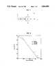
- FIG. 2is an exemplary plot of the room temperature sheet conductance, d/ ⁇ , versus thinning time for a layer of YBa 2 Cu 3 O 7 on a SrTiO 3 substrate;
- FIG. 3shows an exemplary plot of resistance, normalized to the resistance at 300° K., corresponding to the points (a)-(d) in FIG. 2;
- FIG. 4shows an exemplary plot of the resistance, normalized to the resistance at 275° K., of an initially 4000 ⁇ layer of YBa 2 Cu 3 O 7 on a SrTiO 3 substrate after ion thinning for various periods of time.
- FIG. 1schematically depicts an exemplary device, namely, a weak link dc SQUID, 10, which can advantageously be produced according to the inventive method.
- Portions 20 and 30are "weak links" connecting the superconducting regions 40 and 50.
- Portions 60,70, and 80are insulating regions defining a superconducting loop.
- the "weak links", 20 and 30,are thin smooth films of a planar superconductor fabricated according to the inventive method.
- the inventive methodis most advantageously practiced with a planar metal oxide superconductor.
- the superconductoris a c-axis oriented metal oxide.
- a layer of c-axis oriented YBa 2 Cu 3 O x , with x about 7,is provided on a SrTiO 3 substrate.
- the superconducting layercan be grown on any appropriate substrate using any of a variety of known techniques which include evaporation, sputtering, and laser evaporation.
- At least a portion of the superconducting layeris thinned by exposing the layer to an ion beam.
- the substrate with the layer thereonadvantageously is rotated about an axis normal to the film surface, such rotation typically resulting in improved uniformity of film thickness.
- the rotation ratetypically is not critical. A rate in the range 0.1 to 20 Hz will generally be satisfactory.
- low energy ionspreferably in the range 50 eV to 1000 eV. Below 50 eV there is the possibility that ions will stick to the surface, substantially without removing surface atoms, while above 1000 eV ion damage and implantation typically becomes significant.
- the ionsare chosen from a group of elements consisting of oxygen and those elements that are chemically non-reactive with the superconductor. As is known, the removal rate of surface atoms is directly dependent, among other factors, on the atomic mass of the ions. As a result, in a first embodiment, xenon ions are used since xenon is a heavy inert gas. Other non-reacting gases that can be used as ions include Ar, He, Ne, and Kr. Though oxygen is reactive, it can still be used in the thinning process. Typically, metal oxide superconducting films are oxygen deficient at the surface, and can become more oxygen deficient as result of preferential sputtering. Thus, a small amount of oxygen implantation into the near-surface region of the film may actually improve the superconducting properties of the metal oxide layer.
- the direction of the ion beamforms a grazing angle of incidence in the range 5° to 20° with the layer surface.
- the possibility of ion reflection from the surface, without removal of surface atoms,becomes significant, while for angles greater than about 20° surface damage and ion implantation typically become significant.
- the roughness of c-axis oriented superconducting YBa 2 Cu 3 O 7 layers due to the presence of crystallites of a/b-axis orientationcan be reduced by thinning, in accordance with the inventive method.
- this resultderives primarily from anisotropic thinning rates correlated with the intrinsic anisotropies of atomically layered YBa 2 Cu 3 O 7 .
- the roughness due to mis-orientations in thin films of other planar superconductorswill also be reduced by thinning according to the inventive method.
- control of the thinning processis facilitated by a substantially linear relationship between the thickness to resistivity ratio and the thinning time, typically observed after removal of mis-oriented phases.
- a layer of a planar superconductorcan be accurately thinned to a desired electrical thickness (or equivalently d/ ⁇ which has been defined as the sheet conductance) by using thinning time as a control parameter.
- the linear relationship between the thickness to resistivity ratio and the thinning timeis exemplified by FIG. 2.
- the inventive methodcan be practiced with a substrate temperature near room temperature during the thinning process, it may at times be advantageous to maintain the substrate at a low temperature during thinning.
- Low temperature processingtypically decreases the possibility of defect diffusion in a superconductor film. Processing temperatures in the range between liquid helium temperature (4.2° K.) and liquid nitrogen temperature (77° K.), are currently believed to be most advantageous, since at these temperatures diffusion processes are substantially reduced.
- thinning in accordance with the inventive methodmay even result in an improvement of the crystalline quality of the superconducting film. It is believed that the crystal quality of an as-deposited planar superconducting layer typically is relatively low due to the presence in the film of crystallites of more than one orientation. The crystallites having other than c-axis orientation are removed by the thinning process, leaving an ordered layer of substantially one orientation. Exemplarily, thinning removes the a-axis component from a YBa 2 Cu 3 O 7 thin film layer grown initially as c-axis oriented material. The resulting thinned film has c-axis orientation, and substantially lower Xmin than the as-deposited film.
- thinning according to the inventive methodresults in thin smooth superconductive films that are robust to environmental changes.
- a thinned metal oxide superconductorsuch as YBa 2 Cu 3 O 7 , undergoes less deterioration than an as-deposited film upon exposure to normal atmospheric conditions.
- the T c of the superconductor layer of the final thicknesstypically is still relatively high, even after prolonged exposure to an ion beam, though frequently somewhat reduced from their values at the initial thickness.
- the process of producing an articleis completed by conventional techniques. These techniques may include photolithography, providing electrical contacts, and packaging. Exemplarily, in applications requiring very thin films, the final thickness is in the range of tens of angstroms where typically the initial thickness is in the thousands of angstroms, due to the general difficulty of depositing very thin, continuous films of high T c superconductors.
- Two films of YBa 2 Cu 3 O 7were deposited on the same (100) SrTiO 3 substrate, one film for electrical characterization and the other film for x-ray, SEM, and RBS characterizations.
- the filmswere 2400 ⁇ thick c-axis oriented films made in a three-source evaporator. The films were thinned for a selected time and then measured for electrical, x-ray, SEM, and RBS characterizations. This procedure was repeated until the film thickness approached tens of angstroms.
- the filmswere mounted on a substrate platform which was rotated at approximately 2 Hz and oriented at a 10 degree grazing angle of incidence with respect to the impinging ion beam.
- Xenon ionsextracted from a Kaufman ion source operating at a pressure of 1.5 ⁇ 10 -4 Torr, were used with an energy of 1000 eV and a current density of 150 ⁇ A/cm 2 .
- FIG. 2is a plot of the room temperature sheet conductance (d/ ⁇ ) versus thinning time. After 45 minutes of thinning, the trend in the data is linear (solid line in FIG. 2), hence indicating a uniform thinning rate.
- the final thickness of 40 ⁇ after 170 min of thinning [(d) in FIG. 2]is approximately equal to the 2400 ⁇ starting thickness multiplied by the ratio of the ordinate values for d/ ⁇ at (d) and (a).
- FIG. 3is an exemplary plot of the resistance, normalized to the resistance at 300° K., corresponding to the points (a)-(d) in FIG. 2.
- the filmAfter thinning to an electrical thickness of 40 ⁇ (corresponding to a mere three to four lattice constants), the film still showed a T c of about 40° K. At intermediate thicknesses the film had intermediate values of T c .
- FIG. 4shows an exemplary plot of the resistance, normalized to the resistance at 275° K., after thinning of the film for various periods of time.
- Table 1indicates the electrical thickness and thinning time associated with (a)-(d) in FIG. 4.
Landscapes
- Engineering & Computer Science (AREA)
- Manufacturing & Machinery (AREA)
- Superconductor Devices And Manufacturing Methods Thereof (AREA)
- Superconductors And Manufacturing Methods Therefor (AREA)
Abstract
Description
TABLE 1 ______________________________________ Electrical Thickness Milling Time ______________________________________ (a) 4000Å 0 min. (b) 746Å 260 min. (c) 76Å 303 min. (d) 37Å 306.5 min. ______________________________________
Claims (7)
Priority Applications (1)
| Application Number | Priority Date | Filing Date | Title |
|---|---|---|---|
| US07/398,797US4966885A (en) | 1989-08-25 | 1989-08-25 | Method of producing a device comprising a metal oxide superconductor layer |
Applications Claiming Priority (1)
| Application Number | Priority Date | Filing Date | Title |
|---|---|---|---|
| US07/398,797US4966885A (en) | 1989-08-25 | 1989-08-25 | Method of producing a device comprising a metal oxide superconductor layer |
Publications (1)
| Publication Number | Publication Date |
|---|---|
| US4966885Atrue US4966885A (en) | 1990-10-30 |
Family
ID=23576848
Family Applications (1)
| Application Number | Title | Priority Date | Filing Date |
|---|---|---|---|
| US07/398,797Expired - LifetimeUS4966885A (en) | 1989-08-25 | 1989-08-25 | Method of producing a device comprising a metal oxide superconductor layer |
Country Status (1)
| Country | Link |
|---|---|
| US (1) | US4966885A (en) |
Cited By (22)
| Publication number | Priority date | Publication date | Assignee | Title |
|---|---|---|---|---|
| US5219826A (en)* | 1990-08-20 | 1993-06-15 | Conductus, Inc. | Superconducting junctions and method of making same |
| US5280013A (en)* | 1991-07-05 | 1994-01-18 | Conductus, Inc. | Method of preparing high temperature superconductor films on opposite sides of a substrate |
| US5304535A (en)* | 1990-10-29 | 1994-04-19 | E. I. Du Pont De Nemours And Company | Etching of nanoscale structures on high temperature superconductors |
| EP0791968A1 (en)* | 1996-02-22 | 1997-08-27 | E.I. Du Pont De Nemours And Company | Method for improving the performance of high temperature superconducting thin film wafers |
| US5691279A (en)* | 1993-06-22 | 1997-11-25 | The United States Of America As Represented By The Secretary Of The Army | C-axis oriented high temperature superconductors deposited onto new compositions of garnet |
| WO2000016414A1 (en)* | 1998-09-14 | 2000-03-23 | Commonwealth Scientific And Industrial Research Organisation | Method of fabrication of step edge |
| US6255662B1 (en)* | 1998-10-27 | 2001-07-03 | Axcelis Technologies, Inc. | Rutherford backscattering detection for use in Ion implantation |
| US6605321B1 (en)* | 2000-07-20 | 2003-08-12 | Centre National De La Recherche Scientifique (Cnrs) | Method of treating materials by irradiation |
| US6605225B1 (en)* | 1999-01-26 | 2003-08-12 | Japan Science And Technology Corporation | Method and apparatus for fabricating three dimensional element from anisotropic material |
| US20030224620A1 (en)* | 2002-05-31 | 2003-12-04 | Kools Jacques C.S. | Method and apparatus for smoothing surfaces on an atomic scale |
| US20060172892A1 (en)* | 2002-12-30 | 2006-08-03 | Zhenghe Han | Surface improvement method in fabricating high temperature superconductor devices |
| US20070158303A1 (en)* | 2006-01-12 | 2007-07-12 | Kla-Tencor Technologies Corporation | Structural modification using electron beam activated chemical etch |
| US20070158304A1 (en)* | 2006-01-12 | 2007-07-12 | Kla-Tencor Technologies Corporation | Etch selectivity enhancement in electron beam activated chemical etch |
| CN100336237C (en)* | 2001-12-06 | 2007-09-05 | 清华大学 | Method for modifying ion surface for making high-temperature superconductive device |
| US20070264831A1 (en)* | 2006-01-12 | 2007-11-15 | Kla-Tencor Technologies Corporation | Use of ion implantation in chemical etching |
| US20080103052A1 (en)* | 2002-07-26 | 2008-05-01 | Alex Ignatiev | Superconductor material on a tape substrate |
| US20090010526A1 (en)* | 2006-01-12 | 2009-01-08 | Kla Tencor Technologies Corporation | Tungsten plug deposition quality evaluation method by ebace technology |
| US20160351303A1 (en)* | 2009-10-02 | 2016-12-01 | Ambature, Inc. | Extremely Low Resistance Films and Methods for Modifying or Creating Same |
| US20160351780A1 (en)* | 2009-10-02 | 2016-12-01 | Ambature, Inc. | High Temperature Superconducting Films and Methods for Modifying and Creating Same |
| CN107393941A (en)* | 2017-08-11 | 2017-11-24 | 中国科学技术大学 | Low-temperature microwave source, low-temperature microwave source chip and preparation method thereof |
| CN111799362A (en)* | 2020-07-10 | 2020-10-20 | 北京航空航天大学 | Method for surface modification of material for manufacturing high-temperature superconducting device |
| US11882771B2 (en) | 2021-10-18 | 2024-01-23 | International Business Machines Corporation | Smooth metal layers in Josephson junction devices |
Citations (7)
| Publication number | Priority date | Publication date | Assignee | Title |
|---|---|---|---|---|
| JPS61227183A (en)* | 1985-03-29 | 1986-10-09 | Fuji Photo Film Co Ltd | Flattening method |
| JPS61289635A (en)* | 1985-06-17 | 1986-12-19 | Nippon Telegr & Teleph Corp <Ntt> | Surface flatterning |
| JPS62234329A (en)* | 1986-04-04 | 1987-10-14 | Hitachi Nakaseiki Ltd | Ion milling device |
| US4751563A (en)* | 1984-11-05 | 1988-06-14 | International Business Machines, Corp. | Microminiaturized electrical interconnection device and its method of fabrication |
| JPS63199880A (en)* | 1987-02-16 | 1988-08-18 | Sumitomo Electric Ind Ltd | ion milling equipment |
| JPS63300538A (en)* | 1987-05-29 | 1988-12-07 | Nec Corp | How to form wiring |
| JPS63300537A (en)* | 1987-05-29 | 1988-12-07 | Nec Corp | semiconductor equipment |
- 1989
- 1989-08-25USUS07/398,797patent/US4966885A/ennot_activeExpired - Lifetime
Patent Citations (7)
| Publication number | Priority date | Publication date | Assignee | Title |
|---|---|---|---|---|
| US4751563A (en)* | 1984-11-05 | 1988-06-14 | International Business Machines, Corp. | Microminiaturized electrical interconnection device and its method of fabrication |
| JPS61227183A (en)* | 1985-03-29 | 1986-10-09 | Fuji Photo Film Co Ltd | Flattening method |
| JPS61289635A (en)* | 1985-06-17 | 1986-12-19 | Nippon Telegr & Teleph Corp <Ntt> | Surface flatterning |
| JPS62234329A (en)* | 1986-04-04 | 1987-10-14 | Hitachi Nakaseiki Ltd | Ion milling device |
| JPS63199880A (en)* | 1987-02-16 | 1988-08-18 | Sumitomo Electric Ind Ltd | ion milling equipment |
| JPS63300538A (en)* | 1987-05-29 | 1988-12-07 | Nec Corp | How to form wiring |
| JPS63300537A (en)* | 1987-05-29 | 1988-12-07 | Nec Corp | semiconductor equipment |
Non-Patent Citations (20)
| Title |
|---|
| B. Oh, M. Naito, S. Arnason, P. Rosenthal, R. Barton, M. R. Beasley, T. H. Geballe, R. H. Hammond and A. Kapitulnik, "Critical Current Densities and Transport in Superconducting YBa2 Cu3 O7-x Films Made by Electron Beam Coevaporation", Appl. Phys. Lett., vol. 51, No. 11, pp. 852-854, 1987. |
| B. Oh, M. Naito, S. Arnason, P. Rosenthal, R. Barton, M. R. Beasley, T. H. Geballe, R. H. Hammond and A. Kapitulnik, Critical Current Densities and Transport in Superconducting YBa 2 Cu 3 O 7 x Films Made by Electron Beam Coevaporation , Appl. Phys. Lett., vol. 51, No. 11, pp. 852 854, 1987.* |
| D. Dijkkamp, T. Venkatesan, X. D. Wu, S. A. Shaheen, N. Jisrawi, Y. H. Min Lee, W. L. McLean and M. Croft, Preparation of Y Ba Cu Oxide Superconductor Thin Films Using Pulsed Laser Evaporation from High T c Bulk Material , Appl. Phys. Lett., vol. 51, No. 8, pp. 619 621, 1987.* |
| D. Dijkkamp, T. Venkatesan, X. D. Wu, S. A. Shaheen, N. Jisrawi, Y. H. Min-Lee, W. L. McLean and M. Croft, "Preparation of Y-Ba-Cu Oxide Superconductor Thin Films Using Pulsed Laser Evaporation from High Tc Bulk Material", Appl. Phys. Lett., vol. 51, No. 8, pp. 619-621, 1987. |
| G. C. Hilton, E. B. Harris and D. J. Van Harlingen, "Growth, Patterning, and Weak-Link Fabrication of Superconducting YBa2 Cu3 O7-x Thin Films", Appl. Phys. Lett., vol. 53, No. 12, pp. 1107-1109, 1988. |
| G. C. Hilton, E. B. Harris and D. J. Van Harlingen, Growth, Patterning, and Weak Link Fabrication of Superconducting YBa 2 Cu 3 O 7 x Thin Films , Appl. Phys. Lett., vol. 53, No. 12, pp. 1107 1109, 1988.* |
| H. Tsuge, S. Matsui, N. Matsukura, Y. Kojima and Y. Wada, "Superconducting Lines Fabricated from Epitaxial Y-Ba-Cu-O Films", Japanese J. of Appl. Physics, vol. 27, No. 11, 1988, pp. L2237-L2239. |
| H. Tsuge, S. Matsui, N. Matsukura, Y. Kojima and Y. Wada, Superconducting Lines Fabricated from Epitaxial Y Ba Cu O Films , Japanese J. of Appl. Physics, vol. 27, No. 11, 1988, pp. L2237 L2239.* |
| Koch et al, Extended Abstracts High Temperature Superconductors, Apr. 1987, pp. 81 84.* |
| Koch et al, Extended Abstracts-High Temperature Superconductors, Apr. 1987, pp. 81-84. |
| L. F. Johnson, "Ion Microstructure Fabrication in Optical, Magnetic and Surface Acoustical Technologies", Ion Bombardment Modification of Surfaces: Fundamentals and Applications, Chapter 9, Elsevier, Amsterdam, pp. 361-397, 1984. |
| L. F. Johnson, Ion Microstructure Fabrication in Optical, Magnetic and Surface Acoustical Technologies , Ion Bombardment Modification of Surfaces: Fundamentals and Applications, Chapter 9, Elsevier, Amsterdam, pp. 361 397, 1984.* |
| P. M. Mankiewich, J. H. Scofield, W. J. Skocpol, R. E. Howard, A. H. Dayem and E. Good, "Reproducible Technique for Fabrication of Thin Films of High Transistion Temperature Superconductors", Appl. Phys. Lett., vol. 51, No. 21, pp. 1753-1755, 1987. |
| P. M. Mankiewich, J. H. Scofield, W. J. Skocpol, R. E. Howard, A. H. Dayem and E. Good, Reproducible Technique for Fabrication of Thin Films of High Transistion Temperature Superconductors , Appl. Phys. Lett., vol. 51, No. 21, pp. 1753 1755, 1987.* |
| X.X.Xi, J. Geerk, G. Linker, Q. Li and O. Meyer, "Preparation and Superconducting Properties of Ultrathin YBa2 Cu3 O7-x Films", Appl. Phys. Lett., vol. 54, No. 23, pp. 2367-2369, 1989. |
| X.X.Xi, J. Geerk, G. Linker, Q. Li and O. Meyer, Preparation and Superconducting Properties of Ultrathin YBa 2 Cu 3 O 7 x Films , Appl. Phys. Lett., vol. 54, No. 23, pp. 2367 2369, 1989.* |
| Y. Katoh, M. Asahi, H. Asano and O. Michikami, "Preparation of YBaCuO Thin Film dc SQUID", Japanese J. of Appl. Physics, vol. 27, No. 6, pp. L110-L1112, 1988. |
| Y. Katoh, M. Asahi, H. Asano and O. Michikami, Preparation of YBaCuO Thin Film dc SQUID , Japanese J. of Appl. Physics, vol. 27, No. 6, pp. L110 L1112, 1988.* |
| Y. Nishi, S. Moriya, N. Inoue, S. Tokunaga, T. Shima, "Rapid Rate of Ion Milling for the High Tc YBa2 Cu3 O7-x System", J. of Materials Science Letters, vol. 7, pp. 281-282, 1988. |
| Y. Nishi, S. Moriya, N. Inoue, S. Tokunaga, T. Shima, Rapid Rate of Ion Milling for the High T c YBa 2 Cu 3 O 7 x System , J. of Materials Science Letters, vol. 7, pp. 281 282, 1988.* |
Cited By (31)
| Publication number | Priority date | Publication date | Assignee | Title |
|---|---|---|---|---|
| US5219826A (en)* | 1990-08-20 | 1993-06-15 | Conductus, Inc. | Superconducting junctions and method of making same |
| US5304535A (en)* | 1990-10-29 | 1994-04-19 | E. I. Du Pont De Nemours And Company | Etching of nanoscale structures on high temperature superconductors |
| US5280013A (en)* | 1991-07-05 | 1994-01-18 | Conductus, Inc. | Method of preparing high temperature superconductor films on opposite sides of a substrate |
| US5691279A (en)* | 1993-06-22 | 1997-11-25 | The United States Of America As Represented By The Secretary Of The Army | C-axis oriented high temperature superconductors deposited onto new compositions of garnet |
| EP0791968A1 (en)* | 1996-02-22 | 1997-08-27 | E.I. Du Pont De Nemours And Company | Method for improving the performance of high temperature superconducting thin film wafers |
| US5688383A (en)* | 1996-02-22 | 1997-11-18 | E. I. Du Pont De Nemours And Company | Method for improving the performance of high temperature superconducting thin film wafers |
| GB2357917A (en)* | 1998-09-14 | 2001-07-04 | Commw Scient Ind Res Org | Method of fabrication of step edge |
| GB2357917B (en)* | 1998-09-14 | 2002-05-08 | Commw Scient Ind Res Org | Method of fabrication of step edge |
| US6514774B1 (en)* | 1998-09-14 | 2003-02-04 | Commonwealth Scientific And Industrial Research Organisation | Method of fabrication of step edge |
| WO2000016414A1 (en)* | 1998-09-14 | 2000-03-23 | Commonwealth Scientific And Industrial Research Organisation | Method of fabrication of step edge |
| US6255662B1 (en)* | 1998-10-27 | 2001-07-03 | Axcelis Technologies, Inc. | Rutherford backscattering detection for use in Ion implantation |
| US6605225B1 (en)* | 1999-01-26 | 2003-08-12 | Japan Science And Technology Corporation | Method and apparatus for fabricating three dimensional element from anisotropic material |
| US6605321B1 (en)* | 2000-07-20 | 2003-08-12 | Centre National De La Recherche Scientifique (Cnrs) | Method of treating materials by irradiation |
| CN100336237C (en)* | 2001-12-06 | 2007-09-05 | 清华大学 | Method for modifying ion surface for making high-temperature superconductive device |
| US20030224620A1 (en)* | 2002-05-31 | 2003-12-04 | Kools Jacques C.S. | Method and apparatus for smoothing surfaces on an atomic scale |
| US20080103052A1 (en)* | 2002-07-26 | 2008-05-01 | Alex Ignatiev | Superconductor material on a tape substrate |
| US20060172892A1 (en)* | 2002-12-30 | 2006-08-03 | Zhenghe Han | Surface improvement method in fabricating high temperature superconductor devices |
| US8008207B2 (en)* | 2006-01-12 | 2011-08-30 | Kla-Tencor Technologies Corporation | Use of ion implantation in chemical etching |
| US20070264831A1 (en)* | 2006-01-12 | 2007-11-15 | Kla-Tencor Technologies Corporation | Use of ion implantation in chemical etching |
| US20070158303A1 (en)* | 2006-01-12 | 2007-07-12 | Kla-Tencor Technologies Corporation | Structural modification using electron beam activated chemical etch |
| US20090010526A1 (en)* | 2006-01-12 | 2009-01-08 | Kla Tencor Technologies Corporation | Tungsten plug deposition quality evaluation method by ebace technology |
| US7879730B2 (en) | 2006-01-12 | 2011-02-01 | Kla-Tencor Technologies Corporation | Etch selectivity enhancement in electron beam activated chemical etch |
| US7945086B2 (en) | 2006-01-12 | 2011-05-17 | Kla-Tencor Technologies Corporation | Tungsten plug deposition quality evaluation method by EBACE technology |
| US8052885B2 (en) | 2006-01-12 | 2011-11-08 | Kla-Tencor Corporation | Structural modification using electron beam activated chemical etch |
| US20070158304A1 (en)* | 2006-01-12 | 2007-07-12 | Kla-Tencor Technologies Corporation | Etch selectivity enhancement in electron beam activated chemical etch |
| US11316092B2 (en)* | 2009-10-02 | 2022-04-26 | Ambature, Inc. | High temperature superconducting films and methods for modifying and creating same |
| US20160351780A1 (en)* | 2009-10-02 | 2016-12-01 | Ambature, Inc. | High Temperature Superconducting Films and Methods for Modifying and Creating Same |
| US20160351303A1 (en)* | 2009-10-02 | 2016-12-01 | Ambature, Inc. | Extremely Low Resistance Films and Methods for Modifying or Creating Same |
| CN107393941A (en)* | 2017-08-11 | 2017-11-24 | 中国科学技术大学 | Low-temperature microwave source, low-temperature microwave source chip and preparation method thereof |
| CN111799362A (en)* | 2020-07-10 | 2020-10-20 | 北京航空航天大学 | Method for surface modification of material for manufacturing high-temperature superconducting device |
| US11882771B2 (en) | 2021-10-18 | 2024-01-23 | International Business Machines Corporation | Smooth metal layers in Josephson junction devices |
Similar Documents
| Publication | Publication Date | Title |
|---|---|---|
| US4966885A (en) | Method of producing a device comprising a metal oxide superconductor layer | |
| US5968877A (en) | High Tc YBCO superconductor deposited on biaxially textured Ni substrate | |
| US6899928B1 (en) | Dual ion beam assisted deposition of biaxially textured template layers | |
| Murakami | Thermal strain in thin lead films III: Dependences of the strain on film thickness and on grain size | |
| Iijima et al. | Growth structure of yttria-stabilized-zirconia films during off-normal ion-beam-assisted deposition | |
| Groves et al. | Ion-beam assisted deposition of bi-axially aligned MgO template films for YBCO coated conductors | |
| Jia et al. | Effect of chemical and ion‐beam etching on the atomic structure of interfaces in YBa2Cu3O7/PrBa2Cu3O7 Josephson junctions | |
| Yun et al. | Fabrication of c‐oriented HgBa2Ca2Cu3O8+ δ superconducting thin films | |
| Kuwasawa et al. | Observation of anomalous transition in the upper critical fields of Nb/Nb0. 5Zr0. 5 multilayers | |
| US5225398A (en) | Method for forming an oxide superconducting film having different crystal orientation on different regions of a si substrate | |
| Tanaka et al. | Epitaxial growth of MgO layer on Y1Ba2Cu3O7-y thin film | |
| Aarnink et al. | Oxygen transport in c-axis-oriented high-T c superconducting YBa 2 Cu 3 O 7− δ thin films, studied in situ by ellipsometry | |
| EP0297617B1 (en) | Oxide-superconducting device | |
| Ramesh et al. | Thin film Y Ba Cu O high Tc superconductors: structure-property relationships | |
| US5364836A (en) | Article comprising a superconductor/insulator layer structure, and method of making the article | |
| EP0487421B1 (en) | Process for preparing a thin film of Bi-type oxide superconductor | |
| Laubacher et al. | Processing and yield of Y/sub 1/Ba/sub 2/Cu/sub 3/O/sub 7-x/thin films and devices produced with a BaF/sub 2/process | |
| EP0476617B1 (en) | Superconductor junction structure and process for fabricating the same | |
| US5314870A (en) | Preparing thin film of oxide superconductor | |
| Choi et al. | Dependence of superconductivity on the crystallinity of Nb films on Si wafers | |
| Leca et al. | MICROSTRUCTURAL AND ELECTRICAL TRANSPORT PROPERTIES OF RBa2Cu3O7–δ (R= Y, Pr) BASED THIN FILMS AND RAMP-TYPE JOSEPHSON JUNCTIONS | |
| Yang et al. | In situ layer‐by‐layer growth of YBa2Cu3O7− x thin films by multitarget sputter deposition | |
| Braginski et al. | In-situ fabrication, processing and characterization of superconducting oxide films | |
| Blamire et al. | Effects of fabrication conditions on the properties of SIS tunnel junctions | |
| Krauss et al. | Computer-controlled ion beam deposition systems for high Tc superconductor and other multi-component oxide thin films and layered structures |
Legal Events
| Date | Code | Title | Description |
|---|---|---|---|
| AS | Assignment | Owner name:BELL TELEPHONE LABORATORIES, INCORPORATED, NEW JER Free format text:ASSIGNMENT OF ASSIGNORS INTEREST.;ASSIGNOR:HEBARD, ARTHUR F.;REEL/FRAME:005124/0477 Effective date:19890804 Owner name:AMERICAN TELEPHONE & TELEGRAPH COMPANY, NEW YORK Free format text:ASSIGNMENT OF ASSIGNORS INTEREST.;ASSIGNOR:HEBARD, ARTHUR F.;REEL/FRAME:005124/0477 Effective date:19890804 | |
| STCF | Information on status: patent grant | Free format text:PATENTED CASE | |
| FEPP | Fee payment procedure | Free format text:PAYOR NUMBER ASSIGNED (ORIGINAL EVENT CODE: ASPN); ENTITY STATUS OF PATENT OWNER: LARGE ENTITY | |
| FPAY | Fee payment | Year of fee payment:4 | |
| FEPP | Fee payment procedure | Free format text:PAYER NUMBER DE-ASSIGNED (ORIGINAL EVENT CODE: RMPN); ENTITY STATUS OF PATENT OWNER: LARGE ENTITY Free format text:PAYOR NUMBER ASSIGNED (ORIGINAL EVENT CODE: ASPN); ENTITY STATUS OF PATENT OWNER: LARGE ENTITY | |
| FEPP | Fee payment procedure | Free format text:PAYER NUMBER DE-ASSIGNED (ORIGINAL EVENT CODE: RMPN); ENTITY STATUS OF PATENT OWNER: LARGE ENTITY Free format text:PAYOR NUMBER ASSIGNED (ORIGINAL EVENT CODE: ASPN); ENTITY STATUS OF PATENT OWNER: LARGE ENTITY | |
| FPAY | Fee payment | Year of fee payment:8 | |
| FPAY | Fee payment | Year of fee payment:12 |