US4965828A - Non-volatile semiconductor memory with SCRAM hold cycle prior to SCRAM-to-E2 PROM backup transfer - Google Patents
Non-volatile semiconductor memory with SCRAM hold cycle prior to SCRAM-to-E2 PROM backup transferDownload PDFInfo
- Publication number
- US4965828A US4965828AUS07/333,709US33370989AUS4965828AUS 4965828 AUS4965828 AUS 4965828AUS 33370989 AUS33370989 AUS 33370989AUS 4965828 AUS4965828 AUS 4965828A
- Authority
- US
- United States
- Prior art keywords
- data
- sram
- backup
- voltage
- prom
- Prior art date
- Legal status (The legal status is an assumption and is not a legal conclusion. Google has not performed a legal analysis and makes no representation as to the accuracy of the status listed.)
- Expired - Fee Related
Links
Images


Classifications
- G—PHYSICS
- G06—COMPUTING OR CALCULATING; COUNTING
- G06F—ELECTRIC DIGITAL DATA PROCESSING
- G06F11/00—Error detection; Error correction; Monitoring
- G06F11/07—Responding to the occurrence of a fault, e.g. fault tolerance
- G06F11/14—Error detection or correction of the data by redundancy in operation
- G06F11/1402—Saving, restoring, recovering or retrying
- G06F11/1415—Saving, restoring, recovering or retrying at system level
- G06F11/1441—Resetting or repowering
- G—PHYSICS
- G06—COMPUTING OR CALCULATING; COUNTING
- G06F—ELECTRIC DIGITAL DATA PROCESSING
- G06F12/00—Accessing, addressing or allocating within memory systems or architectures
- G06F12/14—Protection against unauthorised use of memory or access to memory
- G06F12/1408—Protection against unauthorised use of memory or access to memory by using cryptography
- G—PHYSICS
- G06—COMPUTING OR CALCULATING; COUNTING
- G06F—ELECTRIC DIGITAL DATA PROCESSING
- G06F11/00—Error detection; Error correction; Monitoring
- G06F11/07—Responding to the occurrence of a fault, e.g. fault tolerance
- G06F11/0703—Error or fault processing not based on redundancy, i.e. by taking additional measures to deal with the error or fault not making use of redundancy in operation, in hardware, or in data representation
- G06F11/0751—Error or fault detection not based on redundancy
- G06F11/0754—Error or fault detection not based on redundancy by exceeding limits
- G—PHYSICS
- G06—COMPUTING OR CALCULATING; COUNTING
- G06F—ELECTRIC DIGITAL DATA PROCESSING
- G06F11/00—Error detection; Error correction; Monitoring
- G06F11/07—Responding to the occurrence of a fault, e.g. fault tolerance
- G06F11/08—Error detection or correction by redundancy in data representation, e.g. by using checking codes
- G06F11/10—Adding special bits or symbols to the coded information, e.g. parity check, casting out 9's or 11's
- G06F11/1008—Adding special bits or symbols to the coded information, e.g. parity check, casting out 9's or 11's in individual solid state devices
Definitions
- the inventionrelates to non-volatile semiconductor memory systems including a volatile high speed SRAM (static random access memory), a non-volatile E 2 PROM (electrically eraseable programmable read only memory) backup memory, and circuitry for transferring the contents of the SRAM to the E 2 PROM in response to onset of a power interruption or failure.
- SRAMstatic random access memory
- E 2 PROMelectrically eraseable programmable read only memory
- U. S. Pat. No. 4,591,782(Germer, issued May 27, 1986) describes a non-volatile memory incorporated into an electric meter in which volatile semiconductor memory is used in conjunction with a backup capacitor and control circuitry.
- the control circuitrysenses the onset of a power failure.
- the backup capacitorsupplies power to effectuate transfer of some of the data from the volatile semiconductor memory to a non-volatile E 2 PROM backup memory.
- the Germer patentdeals with the problem of "wear out" of the E 2 PROMs by not: immediately transferring data from the non-volatile storage to the E 2 PROMs and instead waiting a fixed amount of time until a preset counter "times out".
- the backup capacitorhas sufficient energy storage to maintain power to critical circuits for a long enough period after power failure to permit transfer of the entire contents of the volatile RAM to the non-volatile E 2 PROM.
- a momentary power outagecauses the voltage of an unregulated DC power supply to fall below a first threshold
- a counteris started, but normal operation of the system continues. If the unregulated DC voltage does not rise above a second threshold that is slightly higher than the first threshold before the counter times out, a processor initiates transfer of data from the voltatile RAM to the non-volatile E 2 PROM. If the regulated supply voltage falls below a third threshold at which the processor is no longer able to reliably maintain its operating conditions, a reset signal is produced to reset the processor.
- the third thresholdis set low enough that all data is safely transferred from the volatile RAM to the non-volatile E 2 PROM before the reset signal is generated.
- the requirement of a backup timer and the circuitry using the three thresholdsincreases overall complexity and cost of the Germer system.
- the timeout period of the backup timeris constant, so if the current drawn by the E 2 PROM and associated circuitry increases with age or if the storage capacity of the backup capacitors is degraded the timeout period of the timer may be inadequate and data may be lost.
- the constant duration timeout perioddoes not permit maximum useage of the storage capacity of the backup capacitor, so unnecessary downloading and uploading may occur for short duration power losses even though the backup supply has the capacity to maintain integrity of data in the volatile RAM for the duration of the power loss.
- NOVORAMsthat combine the functions of an SRAM and an E 2 PROM on a single silicon chip.
- Data from the SRAM portionmay be stored in the non-volatile E 2 PROM portion prior to power loss. However, if power is removed prior to completion of data transfer from the SRAM portion to the E 2 PROM portion, the correctness of data in the E 2 PROM is indeterminate.
- non-volatile memory systemwhich includes a volatile semiconductor RAM and a non-volatile backup memory to which data in the RAM is downloaded during power interruptions and from which data is uploaded into the RAM after power interruptions, wherein the number of downloading operations is minimized in accordance with the duration of power interruption, condition of a backup power source, and current drain of the entire memory system.
- the inventionprovides a system that utilizes a volatile SRAM and a non-volatile backup store implemented by means of E 2 PROMs in which data is transferred from the SRAMs to the E 2 PROMs when the power is turned off or interrupted by using high voltage energy stored in a backup capacitor to provide operating power for at least a long enough period of time to effectuate reliable transfer of data from the SRAM to the E 2 PROM.
- Any drop in input power below a first thresholdcauses operation of the SRAM to be halted as soon as the present cycle of operation is finished.
- An internal power supply voltage applied to the SRAMsis reduced to a minimal maintenance level (e.g., 2 volts), and power to certain other circuitry in the system is cut off.
- the energy stored in the backup capacitoris monitored, and at a time when just enough energy plus a safety factor remains to download all of the data from the SRAM to the E 2 PROM, a controller effectuates downloading of all the data in the SRAM to the E.sup. 2 PROM backup memory.
- a unique row-column parity accumulation and check system"scrubs" errors from data read out of the E 2 PROM during an upload of data from the E 2 PROM to the SRAM.
- the backup capacitor voltageis charged up to and maintained at a selected level of approximately 100 volts while the external power supply is applied to the non-volatile memory system. Accessing of the SRAM by a host computer is halted while the backup capacitor is discharged to supply energy to maintain the reduced data maintenance voltage across the SRAM if the external supply voltage falls below the first threshold. Accessing of the SRAM by the host computer is resumed if the external power supply voltage rises above the first threshold before the backup capacitor voltage falls below a second threshold of approximately 85 volts.
- the backup capacitor voltagefalls below the second threshold, all of the data in the SRAM is downloaded to the E 2 PROM while the backup capacitor is discharged to supply energy to maintain the internal power supply voltage at 5 volts during the entire downloading.
- the backup capacitorstores enough energy when the backup capacitor voltage is at 100 volts to both allow the halted condition to continue for at least one minute and also effectuate complete downloading of data from the SRAM to the E 2 PROM. Power is removed from the E 2 PROM during read or write memory accesses by the host computer and also when the 2 volt data maintenance voltage is being maintained on the SRAM. During downloading, row parity information and column parity information are accumulated and stored in the E 2 PROM along with the data from the SRAM.
- the non-volatile memory systemincludes a plurality of integrated circuit SRAMs and a plurality of integrated circuit E 2 PROMs, each of which is subdivided into a plurality of subsections.
- the downloading operationincludes reading words in a first subsection of a first integrated circuit SRAM and transferring the read data into a corresponding subsection of a first integrated circuit E 2 PROM, and also transferring the read data into corresponding words of a row parity accumulator and also into a column parity accumulator.
- the words in a first subsection of a second integrated circuit SRAMthen are read and exclusively ORed with corresponding words of the row parity accumulator and the results replace corresponding words of the row parity accumulator.
- Each word of the first subsectionalso is exclusively ORed with the word in the column parity accumulator, and the result replaces the same prior word in the column parity accumulator.
- the contents of the row parity accumulator and the column parity accumulatorthen are transferred into a scratch pad section of the E 2 PROM.
- the uploading operationincludes reading the words in a first subsection of the first integrated circuit E 2 PROM and transferring the read data into the first subsection of the SRAM, and also transferring the read data into corresponding words of the row parity accumulator and the column parity accumulator.
- the words in a first subsection of a second integrated circuit E 2 PROMare read and exclusively ORed with the corresponding words of the row parity accumulator and the result replaces the same word of the row parity accumulator.
- the words in the first subsection of the second integrated circuit E 2 PROMalso are exclusively ORed with the contents of the column parity accumulator and the result replaces the contents of the column parity accumulator.
- the row parity data and the column parity dataare compared with previously stored row parity data and column parity data written into the E 2 PROM during a prior downloading operation. An error pattern is produced if a mismatch occurs, and data written into the SRAM is exclusively ORed with the error pattern to correct the data. The corrected data then is written into the SRAM.
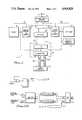
- FIG. 1is a block diagram of the non-volatile semiconductor memory system of the present invention.
- FIG. 2is a schematic circuit diagram of the backup storage capacitor, voltage up converter, and voltage down converter circuitry which cooperate to effectuate transfer of data from the SRAM to the E 2 PROM in the event of a power interruption of at least a minimum specified duration.
- FIG. 3is a detailed block diagram useful in describing the control logic of FIG. 1.
- FIG. 3Ais a detailed block diagram slowing an implementation of the ASIC (application specific integrated circuit) of FIG. 3.
- ASICapplication specific integrated circuit
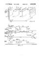
- FIG. 4is a diagram useful in explaining the "bit per chip" row parity and column parity accumulation techniques of the present invention.
- FIG. 5is a timing diagram useful in describing the operation of the system of FIG. 1.
- FIGS. 6A and 6Bare logic diagrams useful in describing certain blocks in FIG. 3A.
- memory system 1includes a volatile RAM (Random Access Memory) section 2, which in the presently preferred embodiment of the invention includes CMOS static RAM cells.
- the SRAM cellspreferably operate reliably to retain data with power supply voltages as low as 2 volts, and operate at normal speeds with V DD , equal to +5 volts.
- SRAM 2is organized as 256k (actually 262,144) words each including 16 data bits and 6 bits of Hamming code data.
- SRAM 2is accessed in response to control circuitry 22 and in conjunction with operation of error detection and correction circuitry 18.
- Control circuitry 22generates addresses on bus 23 for accessing SRAM 2 and E 2 PROM 8.
- Bus 23also includes data conductors, a read conductor, and a write conductor.
- Bus 23also includes 6 Hamming code conductors and 2 parity bit conductors.
- Control circuitry 22is coupled by bus 25 to data input/output circuitry 26, which receives address and control signals on conductors 28. Eighteen Data In conductors 30A and eighteen Data Out conductors 30B are connected to input/output unit 26.
- Poweris supplied to SRAM 2 via a power bus from an energy storage circuit 6 which contains circuitry shown in FIG. 2 to supply a steady internal input power during normal operating conditions and backup power during short duration power interruptions.
- External power bus 10supplies input power at, for example, +5 volts, to energy storage circuit 6.
- Non-volatile memory system 1also includes an E 2 PROM 8.
- Bus 23includes conductors coupled to error detection and correction circuitry 20 and control circuit 22.
- Error detection circuitry 18includes standard Hamming code double bit detection, single bit correction circuitry to "scrub" errors from data read out of SRAM 2.
- Error detection and correction circuitry 20includes row and column parity circuitry and correction circuitry which efficiently "scrubs" errors from data read out of E 2 PROM 8.
- the non-volatile memory system 1 of FIG. 1normally operates as an SRAM when the main power on conductor 10 is present. If there is a power interruption or failure, non-volatile energy system 1 acts as a backup memory that contains all of the data in SRAM 2 immediately before the interruption of input power 10.
- control circuitry 22(which along with SRAM 2 is being sustained by a backup capacitor in energy storage circuit 6) initiates downloading of data from SRAM 2 to E 2 PROM 8 and applies the internal supply voltage to the components as needed to effectuate the downloading.
- downloadingis initiated if the voltage stored on the backup capacitor falls below the predefined threshold, typically about 80% below the nominal backup energy level.
- the controller circuit 22applies full power from the energy storage circuit 6 to all or nearly all of the circuitry in FIG. 1 to effectuate downloading of the entire contents of SRAM 2 into E 2 PROM 8.
- Controller circuit 22controls the sequence of all transfers of data between SRAM 2 and E 2 PROM 8.
- Controller circuit 22also controls all I/O functions and built-in self test and housekeeping functions.
- non-volatile memory 1can be more thoroughly understood by referring to the timing diagram of FIG. 5.
- numeral 32designates an example of a waveform of the input voltage carried by conductor 10.
- Dotted line 33represents a minimum input voltage threshold.
- Input power waveform 32rises from an initial zero level up to a constant operating level, as indicated by numeral 32A.
- Data in E 2 PROM 8then is "uploaded” into SRAM 2 during the interval 38B in the "Data Location" graph in FIG. 5.
- the input voltage 10then falls below the input voltage threshold at point 33A, as indicated by section 32B of waveform 32.
- the input voltagerises as indicated by numeral 32D to level 32E, crossing the input voltage threshold at point 33B and remaining at +5 volts for an indefinite period of time.
- the input voltagefalls below the input voltage threshold at point 33C and remains low for an indefinite time, as indicated by numeral 32F.
- the duration of section 32C of input voltage waveform 32is short enough that non-volatile memory system 1 goes into a "hold mode", which is a low power data maintenance mode, after finishing the present read or write cycle.
- the data of SRAM 2is not downloaded to E 2 PROM 8 unless the backup voltage waveform 35 falls below a "backup voltage threshold" designated by dotted line 36 for more than the minimum hold time.
- the above mentioned backup voltage waveform 35represents the voltage stored on backup capacitor 43 of FIG. 2 as a result of the input power interruptions shown in input voltage waveform 32. More specifically, input voltage waveform 32 causes backup voltage waveform 35 to rise as indicated by numeral 35A, crossing the backup voltage threshold 36 at point 36A and then leveling off as indicated by numeral 35B. The interruption of input power designated by section 32B of input voltage waveform 32 causes a very slow decay of backup voltage waveform 35 between points 35C and 35D. However, backup voltage waveform 35 does not fall below backup voltage threshold 36. When the input voltage waveform 32 then rises as indicated by numeral 32D, backup voltage waveform 35 rises from point 35D to its normal level 35E
- backup voltage waveform 35slowly decays from point 35F to the backup voltage threshold 36, as indicated at point 35G. This initiates downloading of data from SRAM 2 to E 2 PROM 8, resulting in the further decay of backup voltage 35 between points 35G and 35H.
- Data Location graph 38 in FIG. 5indicates the time intervals in which data is stored in the E 2 PROM 8 and SRAM 2, uploaded from E 2 PROM 8 to SRAM 2, and downloaded from to SRAM 2 to E 2 PROM 8.
- both input voltage waveform 32 and backup voltage waveform 35are above their respective thresholds 33 and 36 during initial powering up of non-volatile memory 1, the read/write waveform 40 is at a low level. The powering up operation typically takes approximately 3 seconds.
- Interval 38Bdesignates the time during which data is being uploaded from E 2 PROM 8 to SRAM 2, and typically is approximately 250 milliseconds. Once the transfer is complete, then read/write waveform 40 undergoes transition 40A to level 40B.
- read/write waveform 40is at level 40B
- a host computer 120(FIG. 3) can perform ordinary read and write accesses to SRAM 2.
- E 2 PROM 8 and its associated row and column parity circuitry 20are powered down by control unit 101 of FIG. 3A.
- FIG. 2shows energy storage circuitry 6, which includes a voltage up converter 42 that performs the function of boosting the external 5 volt power supply voltage on conductor 10 to charge up a l,000 to 5,000 microfarad backup capacitor 43 to approximately 100 volts to provide a backup voltage on backup capacitor terminal 65 to power the non-volatile memory system 1.
- a voltage up converter 42that performs the function of boosting the external 5 volt power supply voltage on conductor 10 to charge up a l,000 to 5,000 microfarad backup capacitor 43 to approximately 100 volts to provide a backup voltage on backup capacitor terminal 65 to power the non-volatile memory system 1.
- Control circuit 101(FIG. 3A) supplies separate control voltages to conductors 91A, 91B, and 91C to distribute the internal 5 volt supply voltage on conductor 91 to conductors 12, 14, and 16, respectively, by selectively turning on MOSFETs 97, 98, and 99. If MOSFET 97 is turned off, a three volt zener diode 92 maintains conductor 12 at 2 volts to provide standby power to SRAM 2. At this low voltage, all data is maintained in SRAM 2 in which the total current drawn by SRAM 2 is reduced to only about a miliampere.
- Voltage up converter 42includes a regulator circuit 46, which may be implemented by means of a Motorola "Universal Switching Regulator Subsystem", part number UA78S40.
- Oscillator 46contains a comparator 48 and an oscillator 47.
- the output of oscillator 47is connected to a pullup resistor and a coupling capacitor 51 and to the input of an amplifier.
- the amplifierincludes NPN transistors 52, 55, and 57, diode 53, and resistors 54, 56, and 58. This amplifier provides a 6-to-1 duty cycle pulse signal to the base of NPN transistor 60, producing current to charge inductor 61. When the transistor 60 is turned off, a back emf is generated across inductor 61, forward biasing diode 62.
- switch 49initially is momentarily closed, charging conductor 91 to 5 volts, and thereby providing a 5 volt internal "jump start" supply voltage to all of the circuits in voltage down converter circuit 44.
- Voltage down converter circuit 44includes an oscillator 71 that produces a square wave output that is amplified and shaped by an amplifier including transistors 72, 73, and 77. This amplifier also includes resistors 74 and 76 and capacitor 75, and produces a square wave current pulse through the primary winding of transformer 80.
- the secondary winding of transformer 80is connected between the gate and source of a MOSFET 83.
- the source of MOSFET 83is connected to the cathode of a diode 84, the anode of which is connected to ground.
- transformer 80produces a voltage pulse that turns MOSFET 83 on, causing current to flow from backup capacitor 43 through resistor 88, MOSFET 83, and inductor 69, charging up capacitor 89.
- MOSFET 83is turned off, a back emf across inductor 69 causes the induction current to continue flowing, forward biasing "catch" diode 84 and further charging up capacitor 89 and conductor 91.
- a resistive divider circuit including resistors 63 and 64causes the voltage on the inverting input of comparator 70 to exceed a reference voltage V REF applied to the non-inverting terminal thereof, halting oscillator 71.
- Backup capacitor 43thus is gradually discharged as needed to maintain 5 volts on internal 5 volt conductor 91.
- Comparator 93generates a "Input Power Okay" signal P INOK on conductor 94 by sensing the input supply voltage on conductor 10 by means of a resistive divider circuit that applies a voltage to the non-inverting input of comparator 93.
- V DDis less then +4.5 volts
- P INOKgoes from a "1” to a "0", initiating the above described "hold mode".
- FIG. 3illustrates the organization of SRAM 2, E 2 PROM 8, and ASIC (Application Specific Integrated Circuit) device 115 that includes control circuit 22, Hamming code error detection and correction circuitry 18, row and column parity error detection and correction circuitry 20, and part of input/output circuit 26.
- ASIC 115can be an XC3090 programmable logic gate array manufactured by XILINK. It can be programmed to a wide variety of configurations to establish various input/output formats that might be desirable for input/output circuitry 26.
- a 56 bit magnetic register 111constitutes a "secure key” which is a completely eraseable 56 bit code that is read as a "seed" into an encryption/decryption circuit 112 (FIG. 3A) in ASIC 115 to automatically encrypt data being downloaded from SRAM 2 to E 2 PROM 8 and automatically decrypt seed data when it is being uploaded from E 2 PROM 8 to SRAM 2.
- the 56 bit magnetic registerwhich can be fabricated of ferrite memory cores, can be erased and reset to contain a different "security key” in such a manner that the original key cannot be recovered, at least not at the present state-of-the-art.
- E 2 PROMsmust be rewritten several times in order to reliably erase all evidence of the previously stored data. It is also known that E 2 PROMs require very long write cycles.
- SRAM 2includes sections 2A-1, 2A-2 . . . 2A-8, each of which is a 32,768 word (i.e., 32k) by 16 bit CMOS SRAM, such as an IDT71256L85LB, manufactured by Integrated Device Technology Corp., having its address inputs connected to address bus 28B.
- CMOS SRAMsuch as an IDT71256L85LB, manufactured by Integrated Device Technology Corp.
- the data terminals of each of SRAMs 2A-1 . . . 2A-8are connected to internal data bus 30A,B.
- SRAM 2B-8having address and data terminals connected to address bus 28B and the internal data bus 30A,B also is composed of identical 32k by 8 CMOS SRAMs; this group of SRAMs is used to store Hamming code data.
- SRAM 2also includes an identical 32k word by 16 CMOS SRAM scratch pad memory 2C having its data terminals and address terminals connected to address bus 28B and the data bus 30A,B, respectively.
- the address terminals of the Hamming code data SRAMS 2B-1 . . . 2B-8are connected by conductors 109A to ASIC 115.
- Address buffer 26Abuffers the 18 bit external address bus conductors 28A from the various internal address bus conductors 28B and 28C.
- Data buffers 26B and 26Cbuffer the 18 external Data In conductors 30A and the 18 external Data Out conductors 30B from the internal data bus conductors 30A,B.
- E 2 PROM 8includes sections 8A-1 . . . 8A-8 organized identically (32k words by 16 bits) to data section 2A-1 . . . 2A-8 of SRAM 2.
- the address and data terminals of the E 2 PROMs 8A-1 through 8A-8are connected to the address bus conductors 28B and the data bus conductors 30A,B, respectively.
- E 2 PROM 8also includes an identical 32k word by 16 bit row parity memory 8B having its address and data conductors connected to address bus 28B and data bus 30A,B.
- Column parity and correction data and maintenance data section 8C of E 2 PROM 8also has its address and data terminals connected to address bus 28B and data bus 30A,B.
- FIG. 3Ashows a block diagram representing the functional blocks "programmed" into ASIC 115 in order to accomplish the control, Hamming code generation, row and column parity generation, and checking functions needed to implement the error detection and correction circuits 18 and 20 of FIG. 1.
- Address decode circuit 100receives as inputs 28C the three external higher order addresses A15, A16, and A17 of address bus 28B. Address decode circuit 100 also receives address inputs 107A (A15-A17) produced by address generation circuit 107 in response to either upload sequence circuit 106 or download sequence circuit 10B. Address decode circuit 100 generates nine SRAM chip select conductors 100A and ten E 2 PROM chip select conductors 100B to effectuate the necessary chip select functions for downloading SRAM 2 into E 2 PROM 8, uploading E 2 PROM 8 into SRAM 2, and accessing of SRAM 2 by a host computer 120 via the input/output circuitry 26 of FIG. 1.
- Control circuit 101receives P INOK and E OK on conductors 94 and 96, upload control signals 106A from upload sequencing circuit 106, and download control signals 108A from download sequencing circuit 108.
- Download sequencer circuit 10Bis an ordinary "state machine" circuit that receives control inputs 108A indicating that the input power has fallen below threshold 33 and that the backup capacitor voltage has fallen below threshold 36 (FIG. 5).
- control circuit 101 and address generator 107By communicating back to control circuit 101 and address generator 107, data is transferred from the SRAM 2 to E 2 PROM 8 at the same time that row/column parity data is accumulated.
- the row/column parity controller 105transfers parity data into E 2 PROM 8. This process is repeated 512 times, until all data has been transferred from the SRAM 2 to the E 2 PROM 8.
- Control circuit 101includes both a counter which counts 64 word blocks and the above-mentioned state machine.
- Upload sequencer 106triggers control circuit 101 to generate the necessary timing to generate the read and write signals required for the downloading operation.
- Upload sequencer 106is implemented similarly to download sequencer 108, to transfer data in opposite direction from the E 2 PROM 8 to SRAM 2 wherein both input power and the backup voltage exceed their respective thresholds 33 and 36 (FIG. 5).
- the generated row/column paritiesare compared to the stored parities for the determination of the failure locations so that uploaded data can be corrected.
- Control circuit 101receives data error information 102A from Data In parity check circuit 102, and also receives external read and external write signals and control signals on bus 101A. Control circuit 101 also receives control signals generated by host computer 120 on bus 101A. Control block 101 is configured to provide back plane timing signals and protocol and internal SRAM and E 2 PROM timing. The timing element input is a delay line which is triggered by either an external cycle initiate trigger signal or an internal trigger stimulus. External trigger signals are the result of a request for read/write cycles from the host processor 120. Internal trigger signals result from internal requests for transfers, i.e., transferring data from SRAM 2 to E 2 PROM 8 or vice versa.
- Control circuit 101After an initial edge on the delay on a delay line following edges are produced by the conventional delay line circuitry at 25 nanosecond intervals, and suitable gain circuitry is provided to generate timing signals used to produce the sequence of handshaking required by the host computer 120, the setup timing, the hold times, and the access, read, and write timing signals required by SRAM 2 and E 2 PROM 8 for an uploading or a downloading operation.
- Control circuit 101also includes a mode sensing circuit which determines if a particular cycle is a read cycle or a write cycle.
- the time sequence controlling data flow through the data input latch in block 102, the encryptor/decryptor circuit 112, the Hamming code generator 109, the Hamming comparator/corrector circuit 110, and the Data Out parity check circuit 104, and the column parity accumulator 103can be processed.
- the control circuit 101also provides feedback to the upload sequencer 106 and the download sequencer 108 allowing them to "bump" to the next address or sequence during the data transfers.
- Column parity accumulator 103performs exclusive OR functions necessary to accumulate column parity, as subsequently explained with reference to FIG. 4.
- column parity accumulator 103includes a 16 bit exclusive OR register, each bit of which may have the configuration shown in FIG. 6A, where i represents a particular bit of the lower and upper data bytes on data bus 30A,B. For each bit, if a particular logic level already is stored in the D type latch, and if the next value of the same bit loaded into the register is of the opposite logic level, a mismatch will be produced, and a "1" will appear on the output terminal 102C-i.
- Row/column parity accumulator control circuit 105is used to control transfer of parity data from internal registers to scratch pad SRAM 2C, and then from scratch pad SRAM 2C into E 2 PROM 8. During upload operations row/column parity accumulator control circuit 105 controls the comparison of generated parities to the previously stored parities and then helps effectuate correction of failed locations, as explained subsequently with reference to FIG. 4.
- Data In parity check circuit 102latches data from internal data bus 30A,B, performs a parity check on the 18 bits on data bus 30A,B, generates a data error signal on conductor 102A if an error is detected, and makes the latched data available to column parity accumulator 103 via conductors 102C or to encryptor/decryptor circuit 112 if it is presently enabled. If encryptor/decryptor circuit 112 is presently disabled, Data In parity check circuit 102 makes the latched data available to bus 112A, and hence to Hamming code generator 109 and Hamming comparator/corrector circuit 110.
- the parity checkis a dual byte parity check which involves exclusive ORing of the first data byte D0, D1 . . . D7 with the first (lower byte) parity bit D8 and logically ORing that with the exclusive OR of the second byte of data D9, D10 . . . D16 and the second (upper byte) parity bit which is D17.
- This expressionproduces the data error signal on conductor 102, as indicated by the following equation:
- Data Out parity generator 104receives 16 bits of data via bus 103A from column parity accumulator 103 and generates the parity bits D8 and D17 for the lower and upper bytes of data, respectively. It receives corrected data from Hamming comparator/corrector 110 via bus 110C, and also performs the function of driving data bus 30A,B.
- the following equationsshow that lower parity bit D8 is the exclusive OR of the lower data bits D0, D1 . . . D7 on corrected data bus 110C, and upper parity bit D17 is the exclusive OR of bits D9 through D16 on corrected data bus 110C:
- Encryptor/decryptor circuit 112receives an enable/disable signal on conductor 101D from controller 101 to perform an encryption/decryption function during downloading and uploading. Encryptor/decryptor circuit 112 is bypassed during accessing of SRAM 2 by host computer 120. Encryptor/decryptor circuit 112 receives a 56 bit "security key" from fully eraseable 56 bit magnetic register 111 serially via conductor 111A. During upload or download operations the encrypted/decrypted output is supplied on bus 112A to Hamming code generator 109 and Hamming comparator/corrector 110.
- Encryptor/decryptor circuit 112could be implemented by using a Western Digital WD2001/WD2002 encryption/decryption devices which are designed to encrypt and decrypt 64-bit blocks of data using the algorithms specified in the Federal Information Processing Data Encryption Standard No. 46 using a 56 bit user-specified key to produce a 64-bit cipher text word.
- the publicly known algorithmcan be programmed into the ASIC 115, which is the applicant's preferred embodiment.
- the Western Digital Corporation June, 1984 Communication Products Handbookprovides a detailed explanation and an application note.
- Hamming code generator 109receives the 16 bits of latched data present on bus 112A and generates 6 bits of Hamming data on bus 109A. This is an entirely standard function that can be readily implemented by those skilled in the art from any text on Hamming codes.
- the Hamming code equationsare well known and can be implemented using commercially available circuits or by programming ASIC 115 to exclusive OR the latched and encrypted data bits on bus 112A.
- Hamming comparator/corrector circuit 110receives both the 16 bits of latched data on bus 112A and also receives the 6 bits of Hamming data supplied on bus 109A by Hamming code generator 109 or read out of Hamming data section 2B of SRAM 2.
- Hamming code generator 109regenerates the Hamming codes. The Hamming data that is regenerated is compared to the Hamming data that was previously stored. Based on this comparison, a bit pattern is generated that can then be exclusively ORed with incorrect data to produce the corrected data on bus 110C.
- FIG. 6Bindicates the implementation of Hamming comparator/corrector 110.
- Maintenance control circuit 150performs the function of error logging.
- Data Out parity check circuit 104produces two parity bits which are included with the two byte of corrected data to internal data bus 30A,B.
- the corrected data and its two parity bitscan be read via buffer 26C by host computer 120. If the present data has in fact been corrected, it is also rewritten into SRAM 2 by applying a write command to SRAM 2 in order to write the corrected data into the present address (which still is available on address bus 28B).
- a normal write operation by host computer 120includes addressing SRAM 2 via address bus 28A to generate the chip addresses on internal address bus 28B and the necessary SRAM chip select signals on conductors 100A.
- the data to be writtenis applied to Data Input conductors 30A, including 16 bits of data and two parity bits. This data is latched into Data In parity check circuit 102 and stripped of the parity bits.
- the datais input via bus 112A to Hamming code generator 109 to produce the corresponding Hamming codes on Hamming bus 109A. Then the Hamming data on bus 109A is written into SRAM section 2B, and the data on data bus 30A,B is written in SRAM section 2A.
- the addresses of any errors detected by Hamming comparator/correction circuit 110are stored in the scratch pad section 2C of SRAM 2 along with a count of how many times an error has occurred at that address of SRAM 2 in response to maintenance control circuit 150.
- a downloading operationoccurs when both a P INK signal and an E OK is received by control circuit 101, indicating both loss of input voltage 10 below the input power threshold 33 and loss of the backup voltage 65 below energy threshold 36 (FIG. 5).
- control circuit 101puts the non-volatile memory system 1 into the above-mentioned "hold mode” and turns off MOSFET 91A. (MOSFET 91C already will be off.) Then operating power will be absent from E PROM 8, and SRAM 2 will be powered by a 2 volt standby voltage produced on conductor 12 by 3 volt zener diode 92 in FIG. 2, maintaining all of the data in SRAM 2 with a very low current drain. If the input voltage on conductor 10 returns before the E OK signal is received, the P INOK signal disappears. SRAM 2 and all of control circuitry 22 are supplied by the normal 5 volt levels, and normal read and write operations by host computer 120 are continued.
- control circuit 101triggers download sequencer 108 via one of conductors 108A to download the data of SRAM 2 into E 2 PROM 8.
- Download sequencer 108triggers address generation circuit 107 by means of one of conductors 108B, causing address generation circuit 107 to generate addresses A15-A17 of SRAM 2, causing address decode circuit 100 to generate the corresponding chip select signals on ten conductors 100A to select one of the SRAM chips 2A-1, 2A-2, etc. at a time.
- Download sequencer 108also causes address decode circuit 100 to generate chip select signals 100B to select corresponding E 2 PROM chips 8A-1, 8A-2, etc.
- Address generator 107also generates addresses A0-A14 in response to download sequencer.
- the data on internal data bus 30A,Bis written into the same location of E 2 PROM 8 and also is written into the scratch pad section 2C of SRAM 2 to accumulate row parity data under the control of row/column parity control circuit 105, as subsequently described with reference to FIG. 4.
- the accumulated row parity and column paritythen are written into corresponding locations of scratch pad memory 2C and row parity section 8B of E 2 PROM 8 after scanning of a "row" is complete.
- all of the data and all of the associated row and column parity bits from SRAM 2have been loaded into corresponding locations of E 2 PROM 8.
- An uploading operationis initiated when the P INOK and E OK signals disappear, indicating the return of input voltage on conductor 10 to a value above input voltage threshold 33 and indicating that backup voltage 65 has increased above threshold 36.
- control circuit 101generates a signal on one of conductors 106A causing upload sequencer 106 to produce signals on conductors 106B that trigger address generator 107.
- Address generator 107produces addresses A15-A17 signals on conductors 107A which are decoded by address decode circuit 100 to generate SRAM chip select signals 100A and corresponding E 2 PROM chip select signals 100B to access corresponding locations of E 2 PROM 8 and SRAM 2 as necessary to upload data from E 2 PROM 8 back to SRAM 2.
- Address generator circuit 107also generates the addresses A0-A14 on conductors 28B in response to upload sequencer 106.
- E 2 PROM 8Data read from the accessed location of E 2 PROM 8 appears on internal data bus 30A,B.
- the row parity and column parityare accumulated.
- the row and column parityare checked against the corresponding row and column parity for the previous downloading stored in E 2 PROM section 8B. If a mismatch is found, an error exists in the data transferred to SRAM 2 at the mismatch address.
- An error pattern identifying the mismatchis exclusively ORed in column parity accumulator 103 with the erroneous data in the SRAM, and the corrected data is rewritten into SRAM 2. More specifically, the corrected data is uploaded into the present address of the selected one of SRAM sections 2A-1, 2A-2, . . . 2A-8 by applying a write command to it.
- the corrected data on data bus 30A,Balso is used by Hamming generator 109 to generate correct Hamming codes which are stored at the same address of SRAM section 2B.
- the above processis repeated until all of the data in E 2 PROM 8 has been read out, parity checked, corrected if necessary, corresponding Hamming codes have been generated, the corrected data has been stored in a corresponding one of SRAM sections 2A-1, 2A-2, . . . 2A-8, and the Hamming data has been stored in a corresponding section 2B of SRAM 2.
- data in parity check circuit 102If a data error is detected by data in parity check circuit 102 at the present address, data in parity check circuit 102 produces a data error signal on conductor 102A. This data error signal may be read by host computer 120 to inform it that the present data contains an error.
- numerals 8A-1, 8A-2 . . . 8A-8show three-dimensional representations of sections of E 2 PROM 8 as described above.
- Each section such as 8A-1is subdivided into 512 64 word by 16 bit subsections.
- section 8A-1includes 512 subsections such as subsection 129, which includes 64 words such as 125 and 128 each having 16 bits.
- section 8A-2 of E 2 PROM 8includes 512 subsections 131 each having 64 16 bit words, such as word 130.
- section 8A-8includes 512 64 word subsections 136.
- sections 2A-1, 2A-2 . . . 2A-8 of SRAM 2also each are similarly subdivided into 512 64 word by 16 bit subsections. Row parity accumulation and column parity accumulation are accomplished for SRAM 2 by scanning SRAM 2 in precisely the same fashion as for E 2 PROM 8.
- scratch pad RAM 2Cincludes a single 64 word by 16 bit "row parity accumulator" subsection 132, which includes 64 16 bit words such as 133, 134, etc. Individual corresponding bits of all of the above 64 word by 16 bit subsections of E 2 PROM sections 8A-1 . . . 8A-8, SRAM subsections 2A-1 . . . 2A-8, and 64 word by 16 bit subsection 132 of scratch pad 2C of SRAM 2 are addressed by the same group of address conductors of address bus 28B.
- the group of 64 word by 16 bit subsections 129, 131 . . . 136 of E 2 PROM 8is referred to herein as a "row" for the purpose of describing scanning of E 2 PROM 8 or SRAM 2 to accumulate row and column parities during an upload operation or a download operation of non-volatile memory system 1.
- exclusive OR gates 126, 127, and 137are shown to assist in describing the functions of exclusive ORing corresponding bits on a "bit per chip" basis during "row” scanning to accumulate row and column parity, in accordance with the present invention.
- the first step in the scanning procedureis to sequentially read the contents of the first word 125 in subsection 129. That entire word 125 is stored in the first word 133 of SRAM scratch pad subsection 132. Word 125 also is written into column parity accumulator 103.
- the second word 128 of subsection 129is written into a second word 134 of scratch pad subsection 132, and is exclusively ORed with the contents of column parity accumulator 103 as indicated by Exclusive OR gate 137.
- the resultsreplace the previous contents of column parity accumulator 103.
- the next stepis to repeat the above process for the third 16 bit word and all subsequent 16 bit words of subsection 129. At this point, all of the data in subsection 129 has been transferred to scratch pad section 132, and the column parity for section 129 has been accumulated in column parity accumulator 103.
- subsection 132 of row parity accumulator subsection 132 and the contents of column parity accumulator subsection 141are compared with corresponding row parity and column parity stored during the previous downloading operation into sections 8B and 8C, respectively, of E 2 PROM 8. Simultaneously, all of the data being scanned and read out of E 2 PROM 8 is being written into corresponding locations of SRAM 2. Whenever a mismatch is found between the present row and column parity and the row and column parity stored in sections 8B and 8C of E 2 PROM 8 during the previous downloading operation, that row and column parity is exclusively ORed with the data just read out of the corresponding location of E 2 PROM section 8A to correct the data.
- the result of that exclusive ORingrepresents a two-dimensional map of any erroneous bit positions.
- the third dimension information needed to locate the error preciselyis derived from the exclusive ORing of the column parity information in subsection 141 with previously stored column parity information from the previous downloading operation.
- the result of that exclusive ORingrepresents the erroneous bit positions in the columns of the "row” 129, 131 . . . 136 being scanned. It is necessary to match bit positions in the "row error pattern” and "column error pattern” in order to properly locate the erroneous bit. This is performed by testing these row and column error patterns for each of the sections 8A-1, 8A-2 . . . until a match is found.
- row-column bit matchis obtained by logically ANDing the row error pattern and the column error pattern to produce the "correction data" which then is exclusively ORed with the erroneous data from the SRAM at the identified address.
- the above "row" scanning procedure during uploadingallows corrected data for an entire section such as 8A-1, 8A-2 etc. to be conveniently corrected if necessary and uploaded into SRAM 2, because all of the wrong row and column parity data corresponding to that chip can be stored in sections 8B and 8C and used to correct the erroneous bits.
- the above scanning procedureis particularly advantageous in view of the probable failure modes of SRAM chips, since if there is a failure in one bit of an SRAM chip, the probability of another failure in another bit of the same chip is high.
- E 2 PROM sections 8A-1, 8A-2 . . . 8A-8are replaced by SRAM sections 2A-1, 2A-2 . . . 2A-8.
- the same scratch pad subsections 132 and 141 and the same column parity accumulator 103are used for both uploading and downloading.
- the accumulated row parity data in scratch pad subsection 132 and the accumulated column parity data accumulated in scratch pad section 141are not used to locate and correct errors during downloading, but are simply stored in E 2 PROM sections 8B and 8C at the end of scanning of each "row". The row and column parity data is then available for error correction during the next uploading operation, as described above.
- Appendix 1 attached heretoshows how ASIC 115 can be programmed to produce the configuration of FIG. 3B.
- the above-described non-volatile memory systemprovides a plug-in replacement for a core memory system providing the advantages of non-volatility, and is capable of providing substantially faster access times and cycle times than a comparable core memory. Reliability is greatly increased over that of a core memory system because of the use of integrated circuit components and attendant reduction in the number of solder connections. The amount of power dissipated is much less than that of a comparable core memory, resulting in much less generation of heat and thermal stressing of components and component connections. This contributes greatly to long term reliability.
- the described error detection and correction techniquesfurther increase the reliability of the described memory system over a core memory system replaced thereby. Problems associated with the wear-out phenomena of with E 2 PROMs are avoided.
- the hold mode durationis automatically "self-adjusting" to meet variations in energy stored in the backup capacitor and current drain by circuitry that discharges the backup capacitor during a power interruption due to aging, temperature changes, etc.
- the secure key using a ferrite core register as a completely erasable security key for encryption and decryption of dataprovides the advantage of a secure system which can allow confidential data to be more conveniently “declassified”.
Landscapes
- Engineering & Computer Science (AREA)
- Theoretical Computer Science (AREA)
- Computer Security & Cryptography (AREA)
- Physics & Mathematics (AREA)
- General Engineering & Computer Science (AREA)
- General Physics & Mathematics (AREA)
- Quality & Reliability (AREA)
- Techniques For Improving Reliability Of Storages (AREA)
Abstract
Description
DATA ERROR=(D0 ⊕ D1 ⊕ --- ⊕ D7 ⊕ D8)⊕(D9 ⊕ D10 ⊕ --- ⊕ D16 ⊕ D17)
D8=D0 ⊕ D1 ⊕ --- ⊕ D7
D17=D9 ⊕ D10 ⊕ --- ⊕ D16
Claims (24)
Priority Applications (1)
| Application Number | Priority Date | Filing Date | Title |
|---|---|---|---|
| US07/333,709US4965828A (en) | 1989-04-05 | 1989-04-05 | Non-volatile semiconductor memory with SCRAM hold cycle prior to SCRAM-to-E2 PROM backup transfer |
Applications Claiming Priority (1)
| Application Number | Priority Date | Filing Date | Title |
|---|---|---|---|
| US07/333,709US4965828A (en) | 1989-04-05 | 1989-04-05 | Non-volatile semiconductor memory with SCRAM hold cycle prior to SCRAM-to-E2 PROM backup transfer |
Publications (1)
| Publication Number | Publication Date |
|---|---|
| US4965828Atrue US4965828A (en) | 1990-10-23 |
Family
ID=23303945
Family Applications (1)
| Application Number | Title | Priority Date | Filing Date |
|---|---|---|---|
| US07/333,709Expired - Fee RelatedUS4965828A (en) | 1989-04-05 | 1989-04-05 | Non-volatile semiconductor memory with SCRAM hold cycle prior to SCRAM-to-E2 PROM backup transfer |
Country Status (1)
| Country | Link |
|---|---|
| US (1) | US4965828A (en) |
Cited By (80)
| Publication number | Priority date | Publication date | Assignee | Title |
|---|---|---|---|---|
| US5150412A (en)* | 1990-04-28 | 1992-09-22 | Nec Corporation | Security module for radio telephone |
| US5151855A (en)* | 1989-10-19 | 1992-09-29 | Saturn Corporation | Multiple microprocessor single power supply system shutdown |
| EP0515760A1 (en)* | 1991-05-31 | 1992-12-02 | International Business Machines Corporation | Communication controller having line adapters loadable with an application program |
| US5177371A (en)* | 1990-10-12 | 1993-01-05 | Compaq Computer Corporation | Auxiliary battery operation detection circuit |
| US5177790A (en)* | 1989-12-19 | 1993-01-05 | Bull Cp8 | Method for generating a random number in a data processing system/and system for implementing the method |
| US5241508A (en)* | 1991-04-03 | 1993-08-31 | Peripheral Land, Inc. | Nonvolatile ramdisk memory |
| US5249227A (en)* | 1992-11-30 | 1993-09-28 | Motorola, Inc. | Method and apparatus of controlling processing devices during power transition |
| US5263031A (en)* | 1991-04-15 | 1993-11-16 | Nec Corporation | Semiconductor integrated circuit having post-package testing function for error detection and correction circuit |
| US5272382A (en)* | 1991-06-24 | 1993-12-21 | Compaq Computer Corporation | Power supply for computer system manager |
| US5283905A (en)* | 1991-06-24 | 1994-02-01 | Compaq Computer Corporation | Power supply for computer system manager |
| US5379435A (en)* | 1988-09-06 | 1995-01-03 | Seiko Epson Corporation | Apparatus for providing continuity of operation in a computer |
| US5390322A (en)* | 1991-02-01 | 1995-02-14 | O'brien; Michael J. | Apparatus and method for retaining cycle memory in electronic sterilizer controls |
| US5392438A (en)* | 1989-09-29 | 1995-02-21 | Kabushiki Kaisha Toshiba | Computer system with control unit for controlling power supply to storage unit |
| US5412612A (en)* | 1992-07-08 | 1995-05-02 | Nec Corporation | Semiconductor storage apparatus |
| US5450334A (en)* | 1993-11-01 | 1995-09-12 | Pulizzi Engineering, Inc. | One time programmable switched-output controller |
| US5457748A (en)* | 1992-11-30 | 1995-10-10 | Motorola, Inc. | Method and apparatus for improved security within encrypted communication devices |
| US5506757A (en)* | 1993-06-14 | 1996-04-09 | Macsema, Inc. | Compact electronic data module with nonvolatile memory |
| US5515540A (en)* | 1990-08-27 | 1996-05-07 | Dallas Semiconducter Corp. | Microprocessor with single pin for memory wipe |
| US5539252A (en)* | 1995-05-16 | 1996-07-23 | Macsema, Inc. | Fastener with onboard memory |
| US5815455A (en)* | 1997-09-19 | 1998-09-29 | International Business Machines Corporation | Power supply interface circuit providing nonvolatile storage with suitable operating and standby voltage levels |
| US5826075A (en)* | 1991-10-16 | 1998-10-20 | International Business Machines Corporation | Automated programmable fireware store for a personal computer system |
| US5852737A (en)* | 1995-04-24 | 1998-12-22 | National Semiconductor Corporation | Method and apparatus for operating digital static CMOS components in a very low voltage mode during power-down |
| US5864571A (en)* | 1996-12-11 | 1999-01-26 | International Business Machines Corporation | Error detection circuit using two bit to four bit encoder |
| US5878256A (en)* | 1991-10-16 | 1999-03-02 | International Business Machine Corp. | Method and apparatus for providing updated firmware in a data processing system |
| US5889933A (en)* | 1997-01-30 | 1999-03-30 | Aiwa Co., Ltd. | Adaptive power failure recovery |
| US5937424A (en)* | 1996-09-20 | 1999-08-10 | Intel Corporation | Method and apparatus for suspending the writing of a nonvolatile semiconductor memory with program suspend command |
| US5940861A (en)* | 1996-09-20 | 1999-08-17 | Intel Corporation | Method and apparatus for preempting operations in a nonvolatile memory in order to read code from the nonvolatile memory |
| US6064590A (en)* | 1997-12-09 | 2000-05-16 | Korea Advanced Institute Of Science And Technology | Non-volatile static random access memory device |
| USH1915H (en)* | 1998-12-18 | 2000-11-07 | Cardiac Pacemakers, Inc. | Hybrid static RAM circuit |
| US6189070B1 (en) | 1997-08-28 | 2001-02-13 | Intel Corporation | Apparatus and method for suspending operation to read code in a nonvolatile writable semiconductor memory |
| US6201739B1 (en) | 1996-09-20 | 2001-03-13 | Intel Corporation | Nonvolatile writeable memory with preemption pin |
| US6230319B1 (en)* | 1996-06-03 | 2001-05-08 | Webtv Networks, Inc. | Managing interruption while downloading data over a network |
| US6298421B1 (en)* | 1998-01-12 | 2001-10-02 | Brother Kogyo Kabushiki Kaisha | Data storage device |
| US20020120878A1 (en)* | 2001-02-28 | 2002-08-29 | Lapidus Peter D. | Integrated circuit having programmable voltage level line drivers and method of operation |
| US20020124183A1 (en)* | 2000-12-28 | 2002-09-05 | Stmicroelectronics S.A. | Method and device for protecting integrated circuits against piracy |
| US6449683B1 (en)* | 1999-12-14 | 2002-09-10 | Intel Corporation | Using non-volatile memory for power management in a computer |
| US20020161953A1 (en)* | 2001-04-30 | 2002-10-31 | Kotlowski Kenneth James | Bus arbitrator supporting multiple isochronous streams in a split transactional unidirectional bus architecture and method of operation |
| EP0910016A3 (en)* | 1991-06-10 | 2002-11-13 | Matsushita Electric Industrial Co., Ltd | Apparatus and method for suspending and resuming software applications on a computer |
| US6496939B2 (en)* | 1999-09-21 | 2002-12-17 | Bit Microsystems, Inc. | Method and system for controlling data in a computer system in the event of a power failure |
| US6516415B1 (en)* | 1999-04-23 | 2003-02-04 | Geneticware Co., Ltd | Device and method of maintaining a secret code within an integrated circuit package |
| WO2003073259A1 (en)* | 2002-02-21 | 2003-09-04 | Qualcomm, Incorporated | Direct memory swapping between nand flash and sram with error correction coding |
| US20030217322A1 (en)* | 2002-05-16 | 2003-11-20 | Steve Rodgers | Variable hamming error correction for a one-time-programmable-ROM |
| US6773083B2 (en) | 2001-08-29 | 2004-08-10 | Lexmark International, Inc. | Method and apparatus for non-volatile memory usage in an ink jet printer |
| US6785758B1 (en) | 2001-06-01 | 2004-08-31 | Advanced Micro Devices, Inc. | System and method for machine specific register addressing in a split transactional unidirectional bus architecture |
| US20040225781A1 (en)* | 2001-04-30 | 2004-11-11 | Kotlowski Kenneth James | Split transactional unidirectional bus architecture and method of operation |
| US6839823B1 (en) | 1998-04-21 | 2005-01-04 | Intel Corporation | Increased reliability of data stored on flash memory in applications sensitive to power-loss |
| US20050165999A1 (en)* | 2004-01-27 | 2005-07-28 | Micron Technology, Inc. | Memory device having strobe terminals with multiple functions |
| US20050283343A1 (en)* | 2004-06-18 | 2005-12-22 | International Business Machines Corporation | Methods and arrangements for capturing runtime information |
| US7107480B1 (en) | 2000-12-22 | 2006-09-12 | Simpletech, Inc. | System and method for preventing data corruption in solid-state memory devices after a power failure |
| US20070088923A1 (en)* | 2004-03-08 | 2007-04-19 | Armstrong-Crews Nicholas L | System and method for fast, secure removal of objects from disk storage |
| US20070102529A1 (en)* | 2005-11-08 | 2007-05-10 | Macsema, Inc. | Information devices |
| WO2007079700A1 (en)* | 2006-01-13 | 2007-07-19 | Azd Praha S.R.O. | Method of preserving the safe state of a redundant processor after occurence of a failure |
| US20070180536A1 (en)* | 2005-03-29 | 2007-08-02 | Kabushiki Kaisha Toshiba | Processor, memory, computer system, system LSI, and method of authentication |
| US20080106415A1 (en)* | 2006-11-08 | 2008-05-08 | Macsema, Inc. | Information tag |
| US20080235471A1 (en)* | 2007-03-23 | 2008-09-25 | Michael Feldman | Smart batteryless backup device and method therefor |
| US20090037146A1 (en)* | 2005-11-14 | 2009-02-05 | Trowbridge Jr Jack I | System and methods for testing, monitoring, and replacing equipment |
| US20090132762A1 (en)* | 2007-11-16 | 2009-05-21 | Sony Corporation | Removable nonvolatile memory system with functional inhibition |
| US20090139336A1 (en)* | 2005-11-14 | 2009-06-04 | Trowbridge Jr Jack I | Systems and methods for monitoring system performance |
| US7551470B2 (en) | 2006-10-19 | 2009-06-23 | International Business Machines Corporation | Non volatile memory RAD-hard (NVM-rh) system |
| US20120030540A1 (en)* | 2010-07-29 | 2012-02-02 | Stmicroelectronics (Grenoble) Sas | Ram memory device selectively protectable with ecc |
| US20120198136A1 (en)* | 2009-02-11 | 2012-08-02 | Stec, Inc. | Flash backed dram module including logic for isolating the dram |
| US20120224446A1 (en)* | 2011-03-01 | 2012-09-06 | Agiga Tech Inc. | Capacitor Charge Balance System |
| US8874831B2 (en) | 2007-06-01 | 2014-10-28 | Netlist, Inc. | Flash-DRAM hybrid memory module |
| US8880791B2 (en) | 2007-06-01 | 2014-11-04 | Netlist, Inc. | Isolation switching for backup of registered memory |
| US8904098B2 (en) | 2007-06-01 | 2014-12-02 | Netlist, Inc. | Redundant backup using non-volatile memory |
| US8908453B2 (en)* | 2004-10-26 | 2014-12-09 | Round Rock Research, Llc | Data retention kill function |
| US20150016182A1 (en)* | 2012-01-13 | 2015-01-15 | Mitsubishi Electric Corporation | Sram memory card and voltage monitoring circuit |
| US9436600B2 (en) | 2013-06-11 | 2016-09-06 | Svic No. 28 New Technology Business Investment L.L.P. | Non-volatile memory storage for multi-channel memory system |
| US9436264B2 (en) | 2000-10-23 | 2016-09-06 | Intellectual Ventures Holding 81 Llc | Saving power when in or transitioning to a static mode of a processor |
| US9842628B2 (en) | 2008-07-10 | 2017-12-12 | Agiga Tech Inc. | Capacitor enablement voltage level adjustment method and apparatus |
| EP3326069A4 (en)* | 2015-07-23 | 2018-08-01 | Hewlett-Packard Enterprise Development LP | Preserving volatile memory across a computer system disruption |
| CN108920304A (en)* | 2018-06-20 | 2018-11-30 | 首都师范大学 | The dual threshold method and device for maintaining state are realized in non-volatile memory |
| US10198350B2 (en) | 2011-07-28 | 2019-02-05 | Netlist, Inc. | Memory module having volatile and non-volatile memory subsystems and method of operation |
| US10248328B2 (en) | 2013-11-07 | 2019-04-02 | Netlist, Inc. | Direct data move between DRAM and storage on a memory module |
| US10372551B2 (en) | 2013-03-15 | 2019-08-06 | Netlist, Inc. | Hybrid memory system with configurable error thresholds and failure analysis capability |
| US10380022B2 (en) | 2011-07-28 | 2019-08-13 | Netlist, Inc. | Hybrid memory module and system and method of operating the same |
| US20190392870A1 (en)* | 2015-05-06 | 2019-12-26 | SK Hynix Inc. | Memory module including battery |
| US10838818B2 (en) | 2015-09-18 | 2020-11-17 | Hewlett Packard Enterprise Development Lp | Memory persistence from a volatile memory to a non-volatile memory |
| US10838646B2 (en) | 2011-07-28 | 2020-11-17 | Netlist, Inc. | Method and apparatus for presearching stored data |
| US11257527B2 (en) | 2015-05-06 | 2022-02-22 | SK Hynix Inc. | Memory module with battery and electronic system having the memory module |
Citations (23)
| Publication number | Priority date | Publication date | Assignee | Title |
|---|---|---|---|---|
| US3753001A (en)* | 1971-06-30 | 1973-08-14 | Nissan Motor | Electric power supply system using back-up capacitor |
| US3801963A (en)* | 1972-09-28 | 1974-04-02 | Burroughs Corp | Method and apparatus for transferring data from a volatile data store upon the occurrence of a power failure in a computer |
| US3916390A (en)* | 1974-12-31 | 1975-10-28 | Ibm | Dynamic memory with non-volatile back-up mode |
| US4095046A (en)* | 1975-11-11 | 1978-06-13 | Anstalt Europaische Handelsgesellschaft | Electronic enciphering- and deciphering apparatus in the form of a pocket calculator |
| US4096560A (en)* | 1977-10-28 | 1978-06-20 | Rockwell International Corporation | Protection circuit to minimize the effects of power line interruptions on the contents of a volatile electronic memory |
| US4159517A (en)* | 1976-07-07 | 1979-06-26 | International Business Machines Corporation | Journal back-up storage control for a data processing system |
| US4247913A (en)* | 1979-05-10 | 1981-01-27 | Hiniker Company | Protection circuit for storage of volatile data |
| US4327410A (en)* | 1980-03-26 | 1982-04-27 | Ncr Corporation | Processor auto-recovery system |
| US4348729A (en)* | 1979-04-13 | 1982-09-07 | Hitachi, Ltd. | Engine control system including non-volatile memory and correction data transfer method |
| US4350844A (en)* | 1975-11-20 | 1982-09-21 | Anstalt Europaische Handelsgesellschaft | Encipering- and deciphering apparatus in the form of a typewriter |
| US4375663A (en)* | 1980-03-31 | 1983-03-01 | Leeds & Northrup Company | Power failure early warning circuit for microprocessor with CMOS RAM memory |
| DE3147077A1 (en)* | 1981-11-27 | 1983-06-01 | SWF-Spezialfabrik für Autozubehör Gustav Rau GmbH, 7120 Bietigheim-Bissingen | Electric circuit for storing information in motor vehicles |
| DE3150080A1 (en)* | 1981-12-17 | 1983-07-14 | Franz 7320 Göppingen Schmidt | Radio signalling system |
| US4399524A (en)* | 1980-02-18 | 1983-08-16 | Sharp Kabushiki Kaisha | Memory protection system |
| US4520458A (en)* | 1982-04-22 | 1985-05-28 | Fanuc Ltd | Apparatus for controlling writing of data into a memory having different read and write times |
| US4534018A (en)* | 1983-04-29 | 1985-08-06 | Pitney Bowes Inc. | Non-volatile memory protection circuit with microprocessor interaction |
| US4591782A (en)* | 1984-04-12 | 1986-05-27 | General Electric Company | Power supply and power monitor for electric meter |
| US4612632A (en)* | 1984-12-10 | 1986-09-16 | Zenith Electronics Corporation | Power transition write protection for PROM |
| US4638465A (en)* | 1983-08-04 | 1987-01-20 | Sgs-Ates Componenti Elettronici S.P.A. | Integrated structure microcomputer provided with non-volatile RAM memory |
| US4651307A (en)* | 1984-11-01 | 1987-03-17 | Motorola, Inc. | Non-volatile memory storage system |
| US4658093A (en)* | 1983-07-11 | 1987-04-14 | Hellman Martin E | Software distribution system |
| US4712195A (en)* | 1986-05-09 | 1987-12-08 | Curtis Instruments, Inc. | Solid-state cumulative operations measurement system |
| US4751733A (en)* | 1985-05-15 | 1988-06-14 | Thomson-Csf | Substitution permutation enciphering device |
- 1989
- 1989-04-05USUS07/333,709patent/US4965828A/ennot_activeExpired - Fee Related
Patent Citations (23)
| Publication number | Priority date | Publication date | Assignee | Title |
|---|---|---|---|---|
| US3753001A (en)* | 1971-06-30 | 1973-08-14 | Nissan Motor | Electric power supply system using back-up capacitor |
| US3801963A (en)* | 1972-09-28 | 1974-04-02 | Burroughs Corp | Method and apparatus for transferring data from a volatile data store upon the occurrence of a power failure in a computer |
| US3916390A (en)* | 1974-12-31 | 1975-10-28 | Ibm | Dynamic memory with non-volatile back-up mode |
| US4095046A (en)* | 1975-11-11 | 1978-06-13 | Anstalt Europaische Handelsgesellschaft | Electronic enciphering- and deciphering apparatus in the form of a pocket calculator |
| US4350844A (en)* | 1975-11-20 | 1982-09-21 | Anstalt Europaische Handelsgesellschaft | Encipering- and deciphering apparatus in the form of a typewriter |
| US4159517A (en)* | 1976-07-07 | 1979-06-26 | International Business Machines Corporation | Journal back-up storage control for a data processing system |
| US4096560A (en)* | 1977-10-28 | 1978-06-20 | Rockwell International Corporation | Protection circuit to minimize the effects of power line interruptions on the contents of a volatile electronic memory |
| US4348729A (en)* | 1979-04-13 | 1982-09-07 | Hitachi, Ltd. | Engine control system including non-volatile memory and correction data transfer method |
| US4247913A (en)* | 1979-05-10 | 1981-01-27 | Hiniker Company | Protection circuit for storage of volatile data |
| US4399524A (en)* | 1980-02-18 | 1983-08-16 | Sharp Kabushiki Kaisha | Memory protection system |
| US4327410A (en)* | 1980-03-26 | 1982-04-27 | Ncr Corporation | Processor auto-recovery system |
| US4375663A (en)* | 1980-03-31 | 1983-03-01 | Leeds & Northrup Company | Power failure early warning circuit for microprocessor with CMOS RAM memory |
| DE3147077A1 (en)* | 1981-11-27 | 1983-06-01 | SWF-Spezialfabrik für Autozubehör Gustav Rau GmbH, 7120 Bietigheim-Bissingen | Electric circuit for storing information in motor vehicles |
| DE3150080A1 (en)* | 1981-12-17 | 1983-07-14 | Franz 7320 Göppingen Schmidt | Radio signalling system |
| US4520458A (en)* | 1982-04-22 | 1985-05-28 | Fanuc Ltd | Apparatus for controlling writing of data into a memory having different read and write times |
| US4534018A (en)* | 1983-04-29 | 1985-08-06 | Pitney Bowes Inc. | Non-volatile memory protection circuit with microprocessor interaction |
| US4658093A (en)* | 1983-07-11 | 1987-04-14 | Hellman Martin E | Software distribution system |
| US4638465A (en)* | 1983-08-04 | 1987-01-20 | Sgs-Ates Componenti Elettronici S.P.A. | Integrated structure microcomputer provided with non-volatile RAM memory |
| US4591782A (en)* | 1984-04-12 | 1986-05-27 | General Electric Company | Power supply and power monitor for electric meter |
| US4651307A (en)* | 1984-11-01 | 1987-03-17 | Motorola, Inc. | Non-volatile memory storage system |
| US4612632A (en)* | 1984-12-10 | 1986-09-16 | Zenith Electronics Corporation | Power transition write protection for PROM |
| US4751733A (en)* | 1985-05-15 | 1988-06-14 | Thomson-Csf | Substitution permutation enciphering device |
| US4712195A (en)* | 1986-05-09 | 1987-12-08 | Curtis Instruments, Inc. | Solid-state cumulative operations measurement system |
Cited By (133)
| Publication number | Priority date | Publication date | Assignee | Title |
|---|---|---|---|---|
| US6108792A (en)* | 1988-09-06 | 2000-08-22 | Seiko Epson Corporation | Article for providing continuity of operation in a computer |
| US5848280A (en)* | 1988-09-06 | 1998-12-08 | Seiko Epson Corporation | Apparatus for providing continuity of operation in a computer |
| US5379435A (en)* | 1988-09-06 | 1995-01-03 | Seiko Epson Corporation | Apparatus for providing continuity of operation in a computer |
| US5530877A (en)* | 1988-09-06 | 1996-06-25 | Seiko Epson Corporation | Apparatus for providing continuity of operation in a computer |
| US5392438A (en)* | 1989-09-29 | 1995-02-21 | Kabushiki Kaisha Toshiba | Computer system with control unit for controlling power supply to storage unit |
| US5151855A (en)* | 1989-10-19 | 1992-09-29 | Saturn Corporation | Multiple microprocessor single power supply system shutdown |
| US5177790A (en)* | 1989-12-19 | 1993-01-05 | Bull Cp8 | Method for generating a random number in a data processing system/and system for implementing the method |
| US5150412A (en)* | 1990-04-28 | 1992-09-22 | Nec Corporation | Security module for radio telephone |
| US5515540A (en)* | 1990-08-27 | 1996-05-07 | Dallas Semiconducter Corp. | Microprocessor with single pin for memory wipe |
| US5177371A (en)* | 1990-10-12 | 1993-01-05 | Compaq Computer Corporation | Auxiliary battery operation detection circuit |
| US5390322A (en)* | 1991-02-01 | 1995-02-14 | O'brien; Michael J. | Apparatus and method for retaining cycle memory in electronic sterilizer controls |
| US5241508A (en)* | 1991-04-03 | 1993-08-31 | Peripheral Land, Inc. | Nonvolatile ramdisk memory |
| US5263031A (en)* | 1991-04-15 | 1993-11-16 | Nec Corporation | Semiconductor integrated circuit having post-package testing function for error detection and correction circuit |
| US5235639A (en)* | 1991-05-31 | 1993-08-10 | International Business Machines Corp. | Programmable communication controller line adapter and method for programming line adapter |
| EP0515760A1 (en)* | 1991-05-31 | 1992-12-02 | International Business Machines Corporation | Communication controller having line adapters loadable with an application program |
| EP0910016A3 (en)* | 1991-06-10 | 2002-11-13 | Matsushita Electric Industrial Co., Ltd | Apparatus and method for suspending and resuming software applications on a computer |
| US5283905A (en)* | 1991-06-24 | 1994-02-01 | Compaq Computer Corporation | Power supply for computer system manager |
| US5272382A (en)* | 1991-06-24 | 1993-12-21 | Compaq Computer Corporation | Power supply for computer system manager |
| US5826075A (en)* | 1991-10-16 | 1998-10-20 | International Business Machines Corporation | Automated programmable fireware store for a personal computer system |
| US5878256A (en)* | 1991-10-16 | 1999-03-02 | International Business Machine Corp. | Method and apparatus for providing updated firmware in a data processing system |
| US5412612A (en)* | 1992-07-08 | 1995-05-02 | Nec Corporation | Semiconductor storage apparatus |
| US5249227A (en)* | 1992-11-30 | 1993-09-28 | Motorola, Inc. | Method and apparatus of controlling processing devices during power transition |
| US5457748A (en)* | 1992-11-30 | 1995-10-10 | Motorola, Inc. | Method and apparatus for improved security within encrypted communication devices |
| WO1994013079A1 (en)* | 1992-11-30 | 1994-06-09 | Motorola Inc. | Method and apparatus of controlling processing devices during power transition |
| US5576936A (en)* | 1993-06-14 | 1996-11-19 | Macsema, Inc. | Compact electronic data module with nonvolatile memory |
| US5506757A (en)* | 1993-06-14 | 1996-04-09 | Macsema, Inc. | Compact electronic data module with nonvolatile memory |
| US5450334A (en)* | 1993-11-01 | 1995-09-12 | Pulizzi Engineering, Inc. | One time programmable switched-output controller |
| US5852737A (en)* | 1995-04-24 | 1998-12-22 | National Semiconductor Corporation | Method and apparatus for operating digital static CMOS components in a very low voltage mode during power-down |
| US5539252A (en)* | 1995-05-16 | 1996-07-23 | Macsema, Inc. | Fastener with onboard memory |
| US6230319B1 (en)* | 1996-06-03 | 2001-05-08 | Webtv Networks, Inc. | Managing interruption while downloading data over a network |
| US6201739B1 (en) | 1996-09-20 | 2001-03-13 | Intel Corporation | Nonvolatile writeable memory with preemption pin |
| US6633950B1 (en)* | 1996-09-20 | 2003-10-14 | Intel Corporation | Nonvolatile writeable memory with preemption pin |
| US5937424A (en)* | 1996-09-20 | 1999-08-10 | Intel Corporation | Method and apparatus for suspending the writing of a nonvolatile semiconductor memory with program suspend command |
| US6148360A (en)* | 1996-09-20 | 2000-11-14 | Intel Corporation | Nonvolatile writeable memory with program suspend command |
| US5940861A (en)* | 1996-09-20 | 1999-08-17 | Intel Corporation | Method and apparatus for preempting operations in a nonvolatile memory in order to read code from the nonvolatile memory |
| US5864571A (en)* | 1996-12-11 | 1999-01-26 | International Business Machines Corporation | Error detection circuit using two bit to four bit encoder |
| US5889933A (en)* | 1997-01-30 | 1999-03-30 | Aiwa Co., Ltd. | Adaptive power failure recovery |
| US6189070B1 (en) | 1997-08-28 | 2001-02-13 | Intel Corporation | Apparatus and method for suspending operation to read code in a nonvolatile writable semiconductor memory |
| US5815455A (en)* | 1997-09-19 | 1998-09-29 | International Business Machines Corporation | Power supply interface circuit providing nonvolatile storage with suitable operating and standby voltage levels |
| US6064590A (en)* | 1997-12-09 | 2000-05-16 | Korea Advanced Institute Of Science And Technology | Non-volatile static random access memory device |
| US6298421B1 (en)* | 1998-01-12 | 2001-10-02 | Brother Kogyo Kabushiki Kaisha | Data storage device |
| US6694403B2 (en) | 1998-01-12 | 2004-02-17 | Brother Kogyo Kabushiki Kaisha | Data storage device having download notification means |
| US6839823B1 (en) | 1998-04-21 | 2005-01-04 | Intel Corporation | Increased reliability of data stored on flash memory in applications sensitive to power-loss |
| USH1915H (en)* | 1998-12-18 | 2000-11-07 | Cardiac Pacemakers, Inc. | Hybrid static RAM circuit |
| US6516415B1 (en)* | 1999-04-23 | 2003-02-04 | Geneticware Co., Ltd | Device and method of maintaining a secret code within an integrated circuit package |
| US6496939B2 (en)* | 1999-09-21 | 2002-12-17 | Bit Microsystems, Inc. | Method and system for controlling data in a computer system in the event of a power failure |
| US6449683B1 (en)* | 1999-12-14 | 2002-09-10 | Intel Corporation | Using non-volatile memory for power management in a computer |
| US9436264B2 (en) | 2000-10-23 | 2016-09-06 | Intellectual Ventures Holding 81 Llc | Saving power when in or transitioning to a static mode of a processor |
| US9690366B2 (en) | 2000-10-23 | 2017-06-27 | Intellectual Ventures Holding 81 Llc | Saving power when in or transitioning to a static mode of a processor by using feedback-configured voltage regulator |
| US7269755B2 (en)* | 2000-12-22 | 2007-09-11 | Stec, Inc. | Solid-state memory device with protection against power failure |
| US20070006013A1 (en)* | 2000-12-22 | 2007-01-04 | Simpletech, Inc. | Solid-state memory device with protection against power failure |
| US7107480B1 (en) | 2000-12-22 | 2006-09-12 | Simpletech, Inc. | System and method for preventing data corruption in solid-state memory devices after a power failure |
| US20020124183A1 (en)* | 2000-12-28 | 2002-09-05 | Stmicroelectronics S.A. | Method and device for protecting integrated circuits against piracy |
| US7146509B2 (en)* | 2000-12-28 | 2006-12-05 | Stmicroelectronics Sa | Method and device for protecting integrated circuits against piracy |
| US20020120878A1 (en)* | 2001-02-28 | 2002-08-29 | Lapidus Peter D. | Integrated circuit having programmable voltage level line drivers and method of operation |
| US7058823B2 (en) | 2001-02-28 | 2006-06-06 | Advanced Micro Devices, Inc. | Integrated circuit having programmable voltage level line drivers and method of operation |
| US6813673B2 (en) | 2001-04-30 | 2004-11-02 | Advanced Micro Devices, Inc. | Bus arbitrator supporting multiple isochronous streams in a split transactional unidirectional bus architecture and method of operation |
| US20040225781A1 (en)* | 2001-04-30 | 2004-11-11 | Kotlowski Kenneth James | Split transactional unidirectional bus architecture and method of operation |
| US6912611B2 (en)* | 2001-04-30 | 2005-06-28 | Advanced Micro Devices, Inc. | Split transactional unidirectional bus architecture and method of operation |
| US20020161953A1 (en)* | 2001-04-30 | 2002-10-31 | Kotlowski Kenneth James | Bus arbitrator supporting multiple isochronous streams in a split transactional unidirectional bus architecture and method of operation |
| US6785758B1 (en) | 2001-06-01 | 2004-08-31 | Advanced Micro Devices, Inc. | System and method for machine specific register addressing in a split transactional unidirectional bus architecture |
| US7185128B1 (en) | 2001-06-01 | 2007-02-27 | Advanced Micro Devices, Inc. | System and method for machine specific register addressing in external devices |
| US6773083B2 (en) | 2001-08-29 | 2004-08-10 | Lexmark International, Inc. | Method and apparatus for non-volatile memory usage in an ink jet printer |
| US6683817B2 (en) | 2002-02-21 | 2004-01-27 | Qualcomm, Incorporated | Direct memory swapping between NAND flash and SRAM with error correction coding |
| WO2003073259A1 (en)* | 2002-02-21 | 2003-09-04 | Qualcomm, Incorporated | Direct memory swapping between nand flash and sram with error correction coding |
| US20030217322A1 (en)* | 2002-05-16 | 2003-11-20 | Steve Rodgers | Variable hamming error correction for a one-time-programmable-ROM |
| US7003713B2 (en)* | 2002-05-16 | 2006-02-21 | Broadcom Corporation | Variable Hamming error correction for a one-time-programmable-ROM |
| US20050165999A1 (en)* | 2004-01-27 | 2005-07-28 | Micron Technology, Inc. | Memory device having strobe terminals with multiple functions |
| US7944761B2 (en) | 2004-01-27 | 2011-05-17 | Micron Technology, Inc. | Memory device having strobe terminals with multiple functions |
| US20100265777A1 (en)* | 2004-01-27 | 2010-10-21 | Choi Joo S | Memory device having strobe terminals with multiple functions |
| US7751260B2 (en)* | 2004-01-27 | 2010-07-06 | Micron Technology, Inc. | Memory device having strobe terminals with multiple functions |
| CN101740106A (en)* | 2004-01-27 | 2010-06-16 | 微米技术有限公司 | Memory device having strobe terminals with multiple functions |
| US7508722B2 (en)* | 2004-01-27 | 2009-03-24 | Micron Technology, Inc. | Memory device having strobe terminals with multiple functions |
| US20090231936A1 (en)* | 2004-01-27 | 2009-09-17 | Micron Technology, Inc. | Memory device having strobe terminals with multiple functions |
| US20070088923A1 (en)* | 2004-03-08 | 2007-04-19 | Armstrong-Crews Nicholas L | System and method for fast, secure removal of objects from disk storage |
| US7216207B1 (en)* | 2004-03-08 | 2007-05-08 | International Business Machines Corporation | System and method for fast, secure removal of objects from disk storage |
| US20050283343A1 (en)* | 2004-06-18 | 2005-12-22 | International Business Machines Corporation | Methods and arrangements for capturing runtime information |
| US7177782B2 (en) | 2004-06-18 | 2007-02-13 | Lenovo (Singapore) Pte. Ltd. | Methods and arrangements for capturing runtime information |
| US8908453B2 (en)* | 2004-10-26 | 2014-12-09 | Round Rock Research, Llc | Data retention kill function |
| US20070180536A1 (en)* | 2005-03-29 | 2007-08-02 | Kabushiki Kaisha Toshiba | Processor, memory, computer system, system LSI, and method of authentication |
| US8108941B2 (en)* | 2005-03-29 | 2012-01-31 | Kabushiki Kaisha Toshiba | Processor, memory, computer system, system LSI, and method of authentication |
| US20070102529A1 (en)* | 2005-11-08 | 2007-05-10 | Macsema, Inc. | Information devices |
| US20090139336A1 (en)* | 2005-11-14 | 2009-06-04 | Trowbridge Jr Jack I | Systems and methods for monitoring system performance |
| US7680625B2 (en) | 2005-11-14 | 2010-03-16 | Macsema, Inc. | Systems and methods for monitoring system performance |
| US20100174508A1 (en)* | 2005-11-14 | 2010-07-08 | Trowbridge Jr Jack I | Systems and methods for monitoring system performance |
| US20090037146A1 (en)* | 2005-11-14 | 2009-02-05 | Trowbridge Jr Jack I | System and methods for testing, monitoring, and replacing equipment |
| US7908118B2 (en) | 2005-11-14 | 2011-03-15 | Macsema, Inc. | System and methods for testing, monitoring, and replacing equipment |
| WO2007079700A1 (en)* | 2006-01-13 | 2007-07-19 | Azd Praha S.R.O. | Method of preserving the safe state of a redundant processor after occurence of a failure |
| EA012194B1 (en)* | 2006-01-13 | 2009-08-28 | Ажд Прага С.Р.О. | Method of preserving the safe state of electronic equipment after a failure based on complex safety after occurrence of a failure |
| US7551470B2 (en) | 2006-10-19 | 2009-06-23 | International Business Machines Corporation | Non volatile memory RAD-hard (NVM-rh) system |
| US20080106415A1 (en)* | 2006-11-08 | 2008-05-08 | Macsema, Inc. | Information tag |
| US7908504B2 (en)* | 2007-03-23 | 2011-03-15 | Michael Feldman | Smart batteryless backup device and method therefor |
| US20080235471A1 (en)* | 2007-03-23 | 2008-09-25 | Michael Feldman | Smart batteryless backup device and method therefor |
| US9158684B2 (en)* | 2007-06-01 | 2015-10-13 | Netlist, Inc. | Flash-DRAM hybrid memory module |
| US9928186B2 (en) | 2007-06-01 | 2018-03-27 | Netlist, Inc. | Flash-DRAM hybrid memory module |
| US11016918B2 (en) | 2007-06-01 | 2021-05-25 | Netlist, Inc. | Flash-DRAM hybrid memory module |
| US8874831B2 (en) | 2007-06-01 | 2014-10-28 | Netlist, Inc. | Flash-DRAM hybrid memory module |
| US8880791B2 (en) | 2007-06-01 | 2014-11-04 | Netlist, Inc. | Isolation switching for backup of registered memory |
| US8904098B2 (en) | 2007-06-01 | 2014-12-02 | Netlist, Inc. | Redundant backup using non-volatile memory |
| US8904099B2 (en) | 2007-06-01 | 2014-12-02 | Netlist, Inc. | Isolation switching for backup memory |
| US9921762B2 (en) | 2007-06-01 | 2018-03-20 | Netlist, Inc. | Redundant backup using non-volatile memory |
| US11232054B2 (en) | 2007-06-01 | 2022-01-25 | Netlist, Inc. | Flash-dram hybrid memory module |
| US9269437B2 (en) | 2007-06-01 | 2016-02-23 | Netlist, Inc. | Isolation switching for backup memory |
| US20150242313A1 (en)* | 2007-06-01 | 2015-08-27 | Netlist, Inc. | Flash-dram hybrid memory module |
| US20090132762A1 (en)* | 2007-11-16 | 2009-05-21 | Sony Corporation | Removable nonvolatile memory system with functional inhibition |
| US10134451B1 (en) | 2008-07-10 | 2018-11-20 | Agiga Tech Inc | Adaptive training and adjustment to changing capacitor values based upon age and usage behavior |
| US9842628B2 (en) | 2008-07-10 | 2017-12-12 | Agiga Tech Inc. | Capacitor enablement voltage level adjustment method and apparatus |
| US20120198136A1 (en)* | 2009-02-11 | 2012-08-02 | Stec, Inc. | Flash backed dram module including logic for isolating the dram |
| US8566670B2 (en)* | 2010-07-29 | 2013-10-22 | Stmicroelectronics S.R.L. | RAM memory device selectively protectable with ECC |
| US20120030540A1 (en)* | 2010-07-29 | 2012-02-02 | Stmicroelectronics (Grenoble) Sas | Ram memory device selectively protectable with ecc |
| US20120224446A1 (en)* | 2011-03-01 | 2012-09-06 | Agiga Tech Inc. | Capacitor Charge Balance System |
| US8755243B2 (en)* | 2011-03-01 | 2014-06-17 | Agiga Tech Inc. | Capacitor charge balance system |
| US11561715B2 (en) | 2011-07-28 | 2023-01-24 | Netlist, Inc. | Method and apparatus for presearching stored data |
| US10838646B2 (en) | 2011-07-28 | 2020-11-17 | Netlist, Inc. | Method and apparatus for presearching stored data |
| US10198350B2 (en) | 2011-07-28 | 2019-02-05 | Netlist, Inc. | Memory module having volatile and non-volatile memory subsystems and method of operation |
| US10380022B2 (en) | 2011-07-28 | 2019-08-13 | Netlist, Inc. | Hybrid memory module and system and method of operating the same |
| US9117551B2 (en)* | 2012-01-13 | 2015-08-25 | Mitsubishi Electric Corporation | SRAM memory card and voltage monitoring circuit |
| US20150016182A1 (en)* | 2012-01-13 | 2015-01-15 | Mitsubishi Electric Corporation | Sram memory card and voltage monitoring circuit |
| US11200120B2 (en) | 2013-03-15 | 2021-12-14 | Netlist, Inc. | Hybrid memory system with configurable error thresholds and failure analysis capability |
| US10372551B2 (en) | 2013-03-15 | 2019-08-06 | Netlist, Inc. | Hybrid memory system with configurable error thresholds and failure analysis capability |
| US9996284B2 (en) | 2013-06-11 | 2018-06-12 | Netlist, Inc. | Non-volatile memory storage for multi-channel memory system |
| US10719246B2 (en) | 2013-06-11 | 2020-07-21 | Netlist, Inc. | Non-volatile memory storage for multi-channel memory system |
| US11314422B2 (en) | 2013-06-11 | 2022-04-26 | Netlist, Inc. | Non-volatile memory storage for multi-channel memory system |
| US9436600B2 (en) | 2013-06-11 | 2016-09-06 | Svic No. 28 New Technology Business Investment L.L.P. | Non-volatile memory storage for multi-channel memory system |
| US10248328B2 (en) | 2013-11-07 | 2019-04-02 | Netlist, Inc. | Direct data move between DRAM and storage on a memory module |
| US20190392870A1 (en)* | 2015-05-06 | 2019-12-26 | SK Hynix Inc. | Memory module including battery |
| US11056153B2 (en)* | 2015-05-06 | 2021-07-06 | SK Hynix Inc. | Memory module including battery |
| US11257527B2 (en) | 2015-05-06 | 2022-02-22 | SK Hynix Inc. | Memory module with battery and electronic system having the memory module |
| US11581024B2 (en) | 2015-05-06 | 2023-02-14 | SK Hynix Inc. | Memory module with battery and electronic system having the memory module |
| US12354698B2 (en) | 2015-05-06 | 2025-07-08 | SK Hynix Inc. | Memory module with battery and electronic system having the memory module |
| EP3326069A4 (en)* | 2015-07-23 | 2018-08-01 | Hewlett-Packard Enterprise Development LP | Preserving volatile memory across a computer system disruption |
| US10838818B2 (en) | 2015-09-18 | 2020-11-17 | Hewlett Packard Enterprise Development Lp | Memory persistence from a volatile memory to a non-volatile memory |
| CN108920304A (en)* | 2018-06-20 | 2018-11-30 | 首都师范大学 | The dual threshold method and device for maintaining state are realized in non-volatile memory |
Similar Documents
| Publication | Publication Date | Title |
|---|---|---|
| US4965828A (en) | Non-volatile semiconductor memory with SCRAM hold cycle prior to SCRAM-to-E2 PROM backup transfer | |
| US6345367B1 (en) | Defective memory block handling system by addressing a group of memory blocks for erasure and changing the content therewith | |
| RU2278426C2 (en) | Methods for storing data in energy-independent memorizing devices | |
| US5471478A (en) | Flash EEPROM array data and header file structure | |
| KR100300809B1 (en) | Fault-safe nonvolatile memory programming system and method | |
| US8042021B2 (en) | Memory card and memory controller | |
| KR100386132B1 (en) | Embedded memory redundancy circuit for programmable non-volatile memory and method for programming the same | |
| US8369145B2 (en) | Apparatus and method for detecting over-programming condition in multistate memory device | |
| US6014755A (en) | Method of managing defects in flash disk memories | |
| US6549457B1 (en) | Using multiple status bits per cell for handling power failures during write operations | |
| US7164611B2 (en) | Data retention kill function | |
| US20040202034A1 (en) | Nonvolatile memory with error correction for page copy operation and method thereof | |
| US20120166715A1 (en) | Secure Flash-based Memory System with Fast Wipe Feature | |
| US11875866B2 (en) | Memory programming methods and memory systems | |
| CN101218609B (en) | Portable data carrier with secure data processing | |
| JPS62200600A (en) | Life deciding device for storage element | |
| JP2003198361A (en) | Programmable logic device | |
| TWI300937B (en) | Memory defect detection and self-repair technique | |
| US5001670A (en) | Nonvolatile memory protection | |
| US7200759B2 (en) | Method and device for making information contents of a volatile semiconductor memory irretrievable | |
| CN1163906C (en) | Circuit arrangement with a certain number of electronic circuit components | |
| US6525963B2 (en) | Programmable read-only memory and method for operating the read-only memory | |
| US6275443B1 (en) | Latched row or column select enable driver | |
| EP4552008A1 (en) | Data erasure system | |
| JPH03113656A (en) | semiconductor storage device |
Legal Events
| Date | Code | Title | Description |
|---|---|---|---|
| AS | Assignment | Owner name:QUADRI CORPORATION, A CORP. OF DE, ARIZONA Free format text:ASSIGNMENT OF ASSIGNORS INTEREST.;ASSIGNORS:ERGOTT, HAROLD L. JR.;PETERS, ROBERT E.;RAINWATER, SAM L.;REEL/FRAME:005081/0475;SIGNING DATES FROM 19890404 TO 19890405 | |
| AS | Assignment | Owner name:QUADRI CORPORATION, 300 NORTH MCKEMY, CHANDLER, AZ Free format text:ASSIGNMENT OF ASSIGNORS INTEREST.;ASSIGNOR:BRUDER, JOHN F.;REEL/FRAME:005085/0739 Effective date:19890413 | |
| AS | Assignment | Owner name:PRUDENTIAL INSURANCE COMPANY OF AMERICA, THE Free format text:SECURITY INTEREST;ASSIGNOR:QUADRI ELECTRONICS CORPORATION;REEL/FRAME:005471/0006 Effective date:19900630 | |
| AS | Assignment | Owner name:QUADRI ELECTRONICS CORPORATION, A DE CORP. Free format text:RELEASED BY SECURED PARTY;ASSIGNOR:AMERITRUST COMPANY NATIONAL ASSOCIATION;REEL/FRAME:005557/0170 Effective date:19901224 Owner name:QUADRI ELECTRONICS CORPORATION A DE CORP. Free format text:RELEASED BY SECURED PARTY;ASSIGNOR:PRUDENTIAL INSURANCE COMPANY OF AMERICA, THE;REEL/FRAME:005552/0053 Effective date:19901224 | |
| FEPP | Fee payment procedure | Free format text:PAYOR NUMBER ASSIGNED (ORIGINAL EVENT CODE: ASPN); ENTITY STATUS OF PATENT OWNER: LARGE ENTITY | |
| AS | Assignment | Owner name:OMI ACQUISITION CORPORATION, MASSACHUSETTS Free format text:ASSIGNMENT OF ASSIGNORS INTEREST;ASSIGNOR:QUADRI ELECTRONICS CORPORATION;REEL/FRAME:006916/0543 Effective date:19930521 Owner name:QUADRI ELECTRONICS CORPORATION, ARIZONA Free format text:CHANGE OF NAME;ASSIGNOR:QUADRI CORPORATION;REEL/FRAME:006920/0481 Effective date:19890216 | |
| REMI | Maintenance fee reminder mailed | ||
| AS | Assignment | Owner name:ST MICROWAVE, (ARIZONA) CORPORATION, CALIFORNIA Free format text:NUNC PRO TUNC ASSIGNMENT;ASSIGNOR:OMI ACQUSITION CORPORATION;REEL/FRAME:007036/0034 Effective date:19940510 | |
| LAPS | Lapse for failure to pay maintenance fees | ||
| FP | Lapsed due to failure to pay maintenance fee | Effective date:19941026 | |
| STCH | Information on status: patent discontinuation | Free format text:PATENT EXPIRED DUE TO NONPAYMENT OF MAINTENANCE FEES UNDER 37 CFR 1.362 |