US4963866A - Multi channel digital random access recorder-player - Google Patents
Multi channel digital random access recorder-playerDownload PDFInfo
- Publication number
- US4963866A US4963866AUS07/328,863US32886389AUS4963866AUS 4963866 AUS4963866 AUS 4963866AUS 32886389 AUS32886389 AUS 32886389AUS 4963866 AUS4963866 AUS 4963866A
- Authority
- US
- United States
- Prior art keywords
- memory
- channel
- digital
- board
- channels
- Prior art date
- Legal status (The legal status is an assumption and is not a legal conclusion. Google has not performed a legal analysis and makes no representation as to the accuracy of the status listed.)
- Expired - Fee Related
Links
Images


Classifications
- G—PHYSICS
- G11—INFORMATION STORAGE
- G11C—STATIC STORES
- G11C8/00—Arrangements for selecting an address in a digital store
- G11C8/12—Group selection circuits, e.g. for memory block selection, chip selection, array selection
- G—PHYSICS
- G06—COMPUTING OR CALCULATING; COUNTING
- G06K—GRAPHICAL DATA READING; PRESENTATION OF DATA; RECORD CARRIERS; HANDLING RECORD CARRIERS
- G06K19/00—Record carriers for use with machines and with at least a part designed to carry digital markings
- G06K19/06—Record carriers for use with machines and with at least a part designed to carry digital markings characterised by the kind of the digital marking, e.g. shape, nature, code
- G06K19/067—Record carriers with conductive marks, printed circuits or semiconductor circuit elements, e.g. credit or identity cards also with resonating or responding marks without active components
- G06K19/07—Record carriers with conductive marks, printed circuits or semiconductor circuit elements, e.g. credit or identity cards also with resonating or responding marks without active components with integrated circuit chips
- G—PHYSICS
- G11—INFORMATION STORAGE
- G11C—STATIC STORES
- G11C7/00—Arrangements for writing information into, or reading information out from, a digital store
- G11C7/16—Storage of analogue signals in digital stores using an arrangement comprising analogue/digital [A/D] converters, digital memories and digital/analogue [D/A] converters
- G—PHYSICS
- G11—INFORMATION STORAGE
- G11C—STATIC STORES
- G11C2207/00—Indexing scheme relating to arrangements for writing information into, or reading information out from, a digital store
- G11C2207/16—Solid state audio
Definitions
- the present inventionrelates generally to the field of audio recording and playback systems. More particularly, it relates to the field of digital audio recording and playback systems.
- Typical audio recording systems known in the artuse magnetic tape, drums or disks as storage media for storing audio signals for later playback.
- the storage mediumtypically is mechanically rotated to expose an unwritten section thereof to an electronic unit which records the incoming signal on the medium.
- Such systemssuffer from various disadvantages.
- the mechanical parts of the systemmay wear, especially those parts which rotate or otherwise move.
- the media themselvesmay be damaged in normal use, as when a tape is stretched or a disk is scratched, thereby decreasing the quality of the recording and playback.
- the mechanical parts of those systemsusually require periodic maintenance or replacement.
- Such systemsalso suffer from a limitation on the ability of the user to select randomly a portion of the recording to be played. That is, the messages must be accessed serially, as, for example, by rewinding the recording tape. And the portion of the recording desired may be difficult to locate readily, resulting in excessive search and effort.
- the present inventionis an improvement of the digital recorder/player of U.S. Pat. No. 4,772,873 to the present inventor, which is incorporated herein by reference.
- the present inventionis a modular system for digital random access recording and playback of audio signals.
- a single modulemay comprise one logic board, and up to sixteen channels. Each of the channels may have up to sixteen memory boards per channel.
- a power supply and interconnect cablesalso are provided.
- An entire systemmay comprise several modules. In a system with four modules, for example, there could be four independent audio sources, a crystal controlled master oscillator to provide uniform clocking to the modules, four logic boards, up to 1,024 memory boards, a power supply and interconnect cables.
- a timermay also be provided for timed random access recording and playback.
- an audio signalis picked up and filtered by an analog filter which blocks DC and very low frequencies. Then the signal is filtered by digital filters to prevent foldover distortion of the analog audio signal.
- One of the digital filtersalso preferably generates a clock, although it can be slaved to an external clock.
- the other filters and an analog to digital/digital to analog converter (ADC/DAC)are slaved to the digital filter clock to prevent harmonic heterodyning.
- a master oscillatormay be provided in a system incorporating multiple modules.
- the ADC/DACis a continuous variable slope delta (CVSD) modulator system which samples the analog audio signal at a uniform frequency.
- the digital signal output of the ADCis fed to a memory board.
- the clocking for the CVSD and for the logic boardis derived, through a divide-by-eight counter, from the digital filter clock.
- the logic boardcontrols one module of the system and serves as the controller for the memory boards, an encoder for analog to digital conversion, a decoder for digital to analog conversion, an interface for the system and module controls, and provides clocking for each individual module.
- each module of the system of the present inventionpreferably includes up to sixteen channels, each having up to sixteen memory boards.
- the memory technologymay include CMOS static RAMs, EPROMs or EEPROMs.
- each of the channelsis addressed by a unique four bit binary code and each of the memory boards is addressed by a unique four bit binary code.
- a complete address for a particular memory board of a particular channelis an eight bit code including the unique channel code and the unique board code.
- Each board of a particular channelwill have the same four bits of channel code and a different four bit board code.
- the logic boardcommunicates with the memory of the system via a memory buss which includes a 34 line edge pin connector which connects with all memory boards of the module.
- the logic boardincludes a "D" flip-flop to define the reset and play modes. When power is first applied to the logic board, the logic board resets. Random access for the recording and play modes is achieved by each memory board using two four bit comparators, one which compares the four bit channel code on the memory buss with the setting of a four bit switch, and one which compares the four bit board code on the buss with the four bit switch on the memory board itself.
- An external control switchselects the record or play mode and selects a channel and memory board to receive recorded data or from which data are played back. When there is a match of codes, the memory control logic on an individual memory board is enabled and data is written to or retrieved from a particular memory board.
- the logic boardis also provided with channel and memory board counters for the sequential use of the channels and memory boards in a module. That is, the first memory board of the first channel is filled with messages first, then the second memory board of the first channel, and so on through the sixteenth memory board of the first channel. Then the second channel is enabled, and each of its memory boards is filled sequentially. The process continues until all 256 memory boards of the sixteen channels are filled.
- the present inventionprovides for external control of the channel and memory board selection to provide random access to the memory.
- a selected memory chipis enabled to read incoming data, and data are passed in serial format from the logic board to the selected memory board to be converted to parallel format by a serial to parallel converter, and data are strobed into memory.
- control logic on the memory boardselects a memory chip, the data corresponding to an address supplied by address counters.
- the dataare converted from parallel to serial format by a converter and are transmitted back to the logic board for conversion from digital to analog signals.
- the analog signalis filtered and amplified before passing to an audio signal output device such as a loudspeaker.
- the present inventionovercomes disadvantages and limitations of audio recording systems of the past.
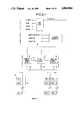
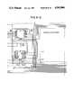
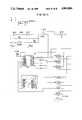
- FIG. 1is a block diagram generally showing the relationships of the main components of one module of a digital audio recording and playback system constructed in accordance with the present invention.
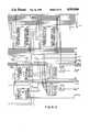
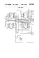
- FIG. 2is a block diagram showing a system according to the present invention having a plurality of the modules shown in FIG. 1.
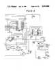
- FIG. 3is a timing diagram for the clocking system of the present invention.
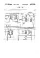
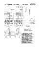
- FIG. 4is a schematic diagram of part of the memory unit of the present invention.
- FIG. 5is a schematic diagram of part of the memory unit of the present invention.
- FIG. 6is a schematic diagram showing the relationships of a variable length message control to the logic board of the present invention.
- FIG. 7is a schematic diagram of part of the logic board of the present invention.
- FIG. 8is a schematic diagram of a part of the logic board of the present invention.
- FIG. 9is a schematic diagram of part of the logic board of the present invention.
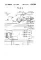
- FIG. 10is a diagram showing the external control unit for the memory boards of the present invention.
- FIG. 11is a schematic diagram showing the external control circuit of the present invention.
- FIG. 12is a schematic diagram of the variable length control of the present invention.
- FIG. 13is a schematic diagram of part of the audio output circuit of the present invention.
- FIG. 14is a schematic diagram of part of the audio output circuit of the present invention.
- FIG. 15is a schematic diagram of part of the audio output circuit of the present invention.
- FIG. 16is a schematic diagram of the master oscillator of the present invention.
- FIG. 1shows a signal processor, including an analog filter 14, a digital filter 16, an ADC/DAC 20, a counter 18 and a clock 17, coupled to a module which includes a logic board 22, an external control 24, a memory buss 28, and a memory board 26.
- Memory board 26includes channel code comparator 25, board code comparator 27, serial-to-parallel/ parallel-to-serial converter 29, memory storage chips 32, memory manager 30 and back-up battery 31.
- An analog signal input 12is filtered by an analog filter system 14 for blocking DC and very low frequencies and by a digital filter 16.
- Circuit 16digitally filters the input signal to prevent foldover distortion of the analog signal during sampling.
- a clock 17generates a clock signal which is used by the entire system. As shown, the single clock signal from clock circuit 17 is a part of digital filter 16, and is divided by counter 18 to provide the correct timing for the other components of the system, as described more fully below.
- ADC/DACanalog-to-digital/digital-to-analog converter
- CVSDcontinuous variable slope delta
- ADC/DAC 20The output of ADC/DAC 20 is fed from logic board 22 which serves as the controller for a memory unit 26 and as an interface with an external control 24, as well as the rest of the system.
- the clocking for memory board 26also is provided by digital filter and clock circuit 17 via counter 18.
- Logic board 22communicates with memory unit 26 via a memory buss 28 which includes a 34 line edge pin connector.
- Memory unit 26may include up to sixteen channels, each of the channels having up to sixteen memory boards 26.
- FIG. 1shows only two representative channels and one representative memory board 26 for each channel.
- Each memory board 26is assigned a unique address and data from logic board 22 may be recorded in memory by sequential filling of each memory board of each channel, if desired. That is, a first memory board 26 of a first channel is filled with data, then the second memory board 26 of the first channel is filled with data, and so on until all memory boards of the first channel are filled. Then, data are entered in the first memory board 26 of the second channel, and so on in sequence. Data may be retrieved in the same sequential manner if desired.
- Each module 11 of recorder-player 10provides random access, both for recording and playback modes when sequential recording and playback is not desired.
- the record modeis selected by the user or by an external control 24, and the correct four bit board and channel codes are strobed in through external control 24 to preset the channel address counter and memory board address counter to the desired channel and board number.
- the selected addressesare placed on memory buss 28 and are fed into two comparators 25 and 27 on memory board 26.
- Comparator 25compares the four bit channel address present on memory buss 28 with the channel addresses set by four bit switch 21 on memory board 26 and comparator 27 compares the four bit board address present on memory 28 with the four bit switch 33 on memory board 26.
- the board and channel comparators 25, 27enable the memory management unit 30 and the address counter 34. Data from logic board 22 may then be written to the memory board 26 with the matching board and address code.
- random access playbackis achieved by the digital recorder-player 10 of the present invention.
- the userby manual or automatic selection, sets a mode switch on external control 24 to playback position and strobes the correct address through the computer port 23 to the external control 24 to select the desired channel and board number.
- the address selection at external control 24is compared by comparators 25 and 27 with the addresses of the channel and board address counters 19 and 15 on the logic unit 22. When a match between the addresses is found, comparators 25 and 27 enable the selected memory board 26 to read and place data in a serial format on memory buss 28 to logic board 22.
- An analog audio input signal 12is converted to digital by ADC/DAC 20 in the record mode.
- the digital data bits from memory unit 26are converted back to the original audio program by ADC/DAC 20.
- the present inventionpreferably includes the continuous - variable - slope - delta modulator system, called CVSD. This system design relies on the delta modulation technique.
- a reference waveformresulting from integrating three output bits, is subtracted from the sampled input waveform. Each output is one bit per sample. If the difference is a positive quantity, the output bit of the next sample will be a "1"; if the difference is negative, the output bit of the next sample will be a "0".
- This reference waveformtherefore, moves positively or negatively by one increment or by one step with each sample.
- the reference waveformis set to zero by initializing the integrators to zero before each message is played or recorded.
- the modulatornow becomes a negative feedback system with output bits which allow the reference waveform to follow the input signal.
- Delta modulationis a special case of differential PCM (Pulse Code Modulation), with only one bit per sample and the output bit rate equal to the sampling frequency.
- CVSDis a particular type of adaptive delta-modulation.
- CVSDrequires no precision components and can be manufactured economically. As all bits have equal weight, isolated bit errors have a very minor audible effect. When combined with the commanding properties of CVSD, differential coding more closely matches the properties of human hearing.
- samples of the analog audio signal 12are taken at a uniform frequency.
- sampled data systemsrequire the output signal to be band limited. This applies to audio.
- This samplinghas been defined by the Nyquist Theorem, Shannon and others.
- the Nyquist theorem derivationassumes a sinusoidal input and employs trigonometric identities to reach a conclusion.
- the sampling frequencymust be higher than the Nyquist frequency to obtain a representative signal.
- Clocking for the digital logic board 22 and ADC/DAC 20advantageously is derived from the clocking frequency of clock 17. This prevents heterodyne and beat frequency interference as all of the clock frequencies are synchronized.
- the clockis determined by an RC time constant or a crystal as part of clock 17.
- external clocksmay be used.
- the resistoris replaced with a trimpot and the capacitor is held constant. This combination of clocking and digital filtering provides any number of audio bandwidth/playtime characteristics. Only one control is required. This digital clocking technique is covered under U.S. Pat. No. 4,772,873.
- the multi-channel recorder-player of the present inventionis a modular concept.
- a minimum configurationcan be made up with one logic board 22 and one memory board 26 (with 2 megabits or 2,048 kilobits of memory) plus power supply and interconnect cable.
- a modulecan be made up with one logic board 22, and up to 16 channels. Each channel may contain up to 16 memory boards 26 per channel.
- a complete modulewould include a logic board 22, a total of 256 memory boards 26 (over 512 megabits or 524,288 kilobits of memory), plus power supply and interconnect cable. Audio bandwidth is controlled by only one simple adjustment from 2.5 kHZ to 10 kHZ. Record/play time per memory board 26 is from 2 minutes 11 seconds at 2.5 kHZ to 33 seconds at 10 kHZ.
- a modulewill have a record/play time from 9 hours 19 minutes at 2.5 kHZ to 2 hours, 11 minutes at 10 kHZ and a 4 module system will be from 37 hours, 18 minutes at 2.5 kHZ to 9 hours, 19 minutes at 10 kHZ.
- the digital random access recorder-player 10 of the present inventioncan include four modules. This provides 4 independent audio sources 37, plus crystal control master oscillator 39, power and interconnect cables. A system could have 4 logic boards and 1,024 memory boards (over 2,147 megabits of memory). Each channel 35 and each memory board 26 in a channel 35 may be addressed in any random manner by an external input from a CPU, manual controller or timer represented in FIG. 1 through external control 24. Control of a single module is possible through a 16-position hex switch, and a start sequence push button represented by manual control board 36 through the computer port represented in FIG. 1 as 23.
- Messagesmay be loaded by direct audio input (-5 dBm, 600 Ohm, unbalanced) or by external digital input, local or remote. Power requirement is from 10 VDC to 15 VDC at less than 100 mA. This remains fairly uniform from a few memory boards 26 per module to many memory boards 26 per module. Low power CMOS chips are used, which only draw current during a transition, and only one memory board 26 and one memory chip is on at any time. Power supply may be a 12 VDC wall plug power supply, battery, solar power system or a thermoelectric generator.
- Audio output per logic boardis approximately 0.5 Watt at 8 Ohms unbalanced.
- a suitable matching transformerwill provide balanced 600 Ohm output.
- the modular concept of the present inventionis also applied to the memory boards 26. They may be removed, installed in any location, digital messages or programs may be loaded internally or externally and may be stored individually on the shelf for years, without loss of program.
- Low power CMOS static RAM memory chipsare used, 8 or less memory chips per board, along with a single lithium battery 31, shown in FIG. 1, for memory retention. This technique is covered by U.S. Pat. No. 4,772,873.
- Lithium battery 31 usecomplies with UL standards (reverse current limited). In the power down mode, standby current is less than 10 microamps per board with a 3 VDC Lithium battery. Expected shelf life of a memory board 26 with a stored program is 8 to 10 years.
- a memory manager chip 30manages the memory by isolating battery 31 when external power is available, and then applying battery 31 to the memory chips 32 if board 26 loses power. Also memory manager 30 provides the user warning if battery 31 begins to lose power by not enabling the user to load a new message.
- a system bussIn order to construct a modular, expandable system, a system buss must be created that will be expandable, and yet require a reasonable number of control lines to operate the external system. Referring to FIG. 1, three busses are defined, one for an external system to control the module, one for local control of the module 23, and a memory buss 28 for communicating to and from the memory boards 26 (using a 34 pin edge board connector).
- the design philosophy of the memory buss 28is to create a system that can access its messages randomly and in any order, not in a serial format like reel-type tape machines or the previous generation digital recorder. (See U.S. Pat. No. 4,772,873). Also, the memory bus 28 function should be independent of the order in which memory boards 26 are connected using separate channel 21 and memory board 33 numbers.
- Table 1The assignment of the pins of memory buss 28 is shown below as Table 1. In accordance with basic digital circuit connections, a line above a description indicates an active low. For example, at pin 17, updown means that when high, count up and when low, count down.
- each channel 35has a unique four-bit binary code.
- Each memory board 26 dedicated to a certain channel 35has the same channel address code and a unique four-bit binary board address code.
- the board 15 and channel 19 address codes on the memory buss 28are compared with the settings on the memory board 26 via two four bit comparators 25 and 27.
- This arrangementallows for 16 channels 35 each with up to 16 memory boards 26 in each channel 35, for a total of 256 memory boards 32.
- address codes of both counters 19 and 15 and counters 21 and 33match, this enables the individual memory board. For example, a simple system might have two messages to be accessed randomly. This would require two channels 35 and as many memory boards 26 as needed for each message. The order of placement of the memory boards 26 would not matter.
- the dataare passed serially from the logic board 22 to the memory board 26, where it is converted to parallel before it is placed into memory.
- More than one clockis present on the bus 28, they differ in both frequency and time. Two clocks run at the rate of the data stream, for use by the serial to parallel and parallel to serial converters. Since each memory address stores eight bits, the data clock is divided by eight and fed to the address counters 34. This division is performed on logic board 22, and then fed through the memory buss 28 (edge pin 15 in Table 1). Two versions of the data clock are used, one advanced slightly in time with respect to the address clock and one slightly delayed. The advanced version of the data clock (edge pin 11 in Table 1) is used during the record sequence, to insure that the data arrives at the memory chips and is stable before the chip reads the data bus.
- the delayed version of the data clock(edge pin 13 in Table 1) is employed to insure that the data is stable before it is converted to serial and sent back to the logic unit. By displacing selected clocks in time, the need to resort to a handshaking timing protocol is avoided.
- a timing diagram for the clocks of the present inventionare shown in FIG. 3.
- the present inventionuses 2 four bit address codes to initialize any given memory board 26.
- U2acts as the memory manager for the memory board 26, performing several important functions. Beside allowing data to be written to memory board 26 when the memory board 26 is selected, U2 also decodes the three most significant bits of the address to enable the individual memory chips, and switches power from VCC or the battery to prevent corruption of the memory. U2 also will not allow access or memory if the voltage across the battery falls below a set limit.
- the present inventionmay use an eight-bit serial to parallel converter to store eight bits of digital system at a time.
- Memory board 26may include a 256K memory organized 8 by 32K.
- the inventioncould use memory board 26 organized as 1 by 256K and avoid the serial to parallel process, but eight bit data buses are currently the industry standard.
- the memory boards 26can also accept a variety of memory technologies. CMOS static RAMs provide instantaneous record and play, while EPROMs and EEPROMs can provide fixed play only.
- Addresses for the memory chipsare provided by dividing the address clock (edge pin 15 in Table 1) by five cascaded fourbit up-down address counters (shown as 34 in FIG. 1) for reverse as well as forward (U15, U16, U17, U18, and U19 in FIG. 4).
- the first 15 least significant binary digits(A0-A14) are used first 15 least significant binary directly by the memory chips as addresses.
- the three most significant digitsare decoded by U2 to enable each memory chip in turn.
- edge pin 7is set high to enable the memory chips to read data and enable the serial to parallel converter, U11 in FIG. 5.
- Datais passed in a serial format from the logic board 22 to the memory board 26 by edge pin 9, converted to parallel by U11, and strobed into memory chips (U3, U4, U5, U6, U7, U8, U9 and U10) by pin 5.
- edge pin 7is pulled low to allow the memory chip selected by U2 to place the data corresponding to the address supplied by address counters 34 on the data bus. This occurs when a memory chip has a stable address input, no strobing is necessary.
- the data on the data busis latched in to the parallel to serial converter (U12) on the rising edge of the address clock (edge pin 15), and clocked out serially by edge pin 13.
- the datais buffered and transmitted back to logic board 22 via edge pin 27 for conversion to analog.
- U12is on all the time, so that during a record cycle, the data is passed back to the logic board 22 so that the user can hear what is actually being recorded, not just the audio source.
- the userhas three switches on memory board 32.
- the first switch, S1 in FIG. 4allows the user to set the system to halt at one of eight positions in memory.
- the inputs of S1are hooked up to either high-order address bits or memory chip enables of memory manager 42. Only one of the eight switches can be closed at one time.
- the outputs of the switchare together and tied to a falling-edge pulse generator, which generates a positive square wave on edge pin 21. This causes logic board 22 to disable the clock, leaving the address counters 34 of memory board 32 as the end of the message.
- the second switch, S2 in FIG. 4,is the chip select switch; it increments the board counter on logic board 22 at one of eight points in memory.
- the inputs of the switchare hooked to the chip enables of memory manager U2, or the most significant bit of the address counters (A18) if the message is to use all the memory available. Only one switch is to be connected at any one time.
- the outputs on the select switchare all tied together and then fed to a falling edge triggered pulse generator. The pulse is buffered and then fed to logic board 22 through edge pin 19. A positive pulse on this line will cause the system to reset address counters 34 and replay from the beginning if restarted.
- the third switchis the last board out switch (S5 in FIG. 5) which when on connects the halt out (edge pin 19) which will cause the channel counters 19 on logic board 22 to reset.
- the other output to logic board 22is the counter strobe out, which is counted by a variable length control (see FIG. 12). It is produced by the board that is active, by adding the output of U14 and U13 in FIG. 5 with a high order address bit, A10.
- Logic board 22controls one module, performing many different functions to control the system. It is the controller, for memory boards 26, the encoder for analog to digital conversion, the decoder for the digital to analog conversion, the interface for system and module control, and provides timing for the individual module.
- a modulecan consist of just one logic board 22 and a memory board 26, or one logic board 22 up to 256 memory boards 26.
- a modulecan be organized into 16 separate channels 26 with up to 16 memory boards 32 per channel. Referring to FIG. 2 channel display and channel select board 38 are options that can be included is a module.
- Logic board 22ties them all together.
- Module control for random accesspreferably is accomplished by use of an external device via a computer interface (J2) shown in Table 3 below and as described more fully below.
- logic board 22communicates through the three separate system buses described above.
- logic board 22communicates through a 34 line edge pin connector memory buss 28 at the back of the board. All memory boards 26 are connected to this memory buss 28.
- Logic board 22receives control command through two busses, one from the system (J1 shown in Table 2) and one from local control (J2 shown in Table 3).
- the analog signal( -5dBm, 600 Ohms, unbalanced) enters through a phono jack on the face of the logic board.
- the analog signal to be recordedis next filtered by a simple RC network R3 and C2 in FIG. 7 in series to block DC and very low frequencies below 70 HZ.
- C3 in FIG. 7 in parallel with groundremoves any radio frequency signals that may be present in the input or that may emanate from the digital filter.
- the analog signalis fed into a two-stage, 12-pole, low-pass, anti-aliasing filter network (U1 and U5 in FIG. 7) to prevent foldover distortion of the analog audio signal when sampled.
- U1 and U5are two National Semiconductor MF6-50 6-pole digital filters cascaded.
- the MF6-50also has op-amps on the chip to buffer the input signal.
- a simple RC networkis used with an op-amps to short any radio or clock frequencies that may couple with the audio line to ground.
- the cutoff frequencyis a function of the sampling period, allowing the user to change the audio bandwidth without changing board components.
- the cutoff frequencyis 1/50th of the filter sampling frequency.
- the MF6-50can generate its own clock or be slaved to an external clock.
- a single module of the present inventiongenerates its own clock from the first MF6-50 (U1).
- all the other MF6-50's and the CVSD chipare slaved to it to prevent harmonic heterodyning (constructive interference of the higher harmonics of the filter clock). If a module is operated as a part of a multiple module system, then all filters are slaved to the system oscillator. All other clocks used by logic board 22 are divided off the filter clock.
- the filter clock frequencyis a function of C24 and R2
- the frequency of the whole modulecan be changed by adjusting R2, a variable resistor. So the upper limit of the audio bandwidth of the recorded signal can be changed very easily.
- the following chartshows the relationship between the sampling frequency, amount of memory, and bandwidth:
- the analog inputis converted to digital by U11 in FIG. 7. Since the audio bandwidth is 1/50th of the filter clock, the CVSD frequency is set at 1/8th of the filter clock to insure that the input signal is not undersampled.
- the CVSD chipoutputs a serial stream of data, which is buffered and placed (still in serial format) on the memory buss where it is recorded into memory. Whether during a play or record cycle, U11 reconstructs an analog signal from the serial digital data. The reconstructed signal is filtered first by a RC network in series (R19 and C12 in FIG. 7) to block DC, and then by C10 in FIG. 7 in parallel with ground to remove any crosstalk from the clocks or radio frequency signals.
- the reconstructed analog signalis low pass filtered by two MF6-50 6-pole digital filters, to remove any high frequency quantization noise that nay be present.
- the two filtersare cascaded to form a 12-pole system. Since the filters are slaved to the filter clock, they have the same cutoff frequency as the input filters.
- Several RC filtersare employed to filter out RF and crosstalk and provide DC bias before final ampliciation by U23 shown in FIG. 8, and the MF6-50 filters themselves have op-amps on board the chips themselves that are used to provide the proper impedance for the filters.
- R42 in FIG. 8is a variable resistor that controls the signal strength of the output.
- the amplifieris a LM386 hi-fidelity audio amplifier with a gain of 20 (approximately 13dB). This produces a 0.5 watt 8 Ohm unbalanced output that may be monitored by a jack on the front panel, fed to a speaker through pin 6 of J2 in Table 3, or fed to an amplifier through pin 5 of J2.
- Timing for logic board 22is provided by dividing down the filter clock.
- the first digital filter, U1 shown in FIG. 5,generates the filter clock from an on-board RC oscillator.
- This filter clockis divided by eight by U2 (a divide by n counter) to produce the data clock, which is used by U11 (FIG. 8) to sample the audio. Since CVSD encoding produces one bit per sample, the data clock and the serial data stream produced by U11 are at the same frequency.
- a delayed version of the data clock(memory buss pin 11 in Table 1) is fed to memory buss 28 for the serial to parallel converter. The delay is necessary for the data to become stable before they are shifted.
- An advanced version of the data clock(memory buss pin 13) is also used in a similar manner to shift data in the parallel to serial process.
- the data clockis divided by eight by U4 (a divide by eight counter shown in FIG. 4) to produce the address clock.
- This clockis divided by the address clocks on the memory boards 26 to produce the address for the memory chips, and it is used to strobe the serial to parallel and parallel to serial converters.
- the basic ideais that in one pulse of the address clock, eight bits of serial data are transmitted, hence another memory location is needed.
- the special featuresare created by manipulating the clock.
- U2By pressing the fast forward button F-F, shown in FIG. 10, on the face of the logic board 22, U2 is changed from a divide by eight to a divide by four counter, thus making the system twice as fast.
- U4is a switch that controls U2.
- the reverse switchalso changes U2 into a divide by four counter, but also pulls the up/down control line (pin 17 on memory buss 28) low which causes the board, channel and address counters to count backwards.
- the modulereverses at a rate two times faster than normal play.
- the pause functionis realized by disabling the clock.
- U7 in FIG. 5, a quad nandthe filter clock is cut off from U2, U3, (the dividers which are cascaded to produce the data and memory clocks) and U11 (the CVSD encoder), thus stopping the system.
- the pause functionintended as an editing tool.
- Logic board 22is controlled by a "D" flip-flop.
- U6 shown in FIG. 4contains the “D” flip-flop and is the heart of logic board 22.
- a power-on-reset circuitWhen power is first applied to the board, a power-on-reset circuit generates a momentary pulse which resets the board and channel counters, (U24 and U25 in FIG. 8) pulses the reset line, (memory buss pin 30) which resets the address counters on all the memory boards and resets the "D" flip-flop into the standby mode.
- the inverted output from the "D" flip-flop (Q bar)resets the frequency dividers U2 and U3.
- the noninverted outputis pulled low, and is tied to the reset of the CVSD encoder (U11). This resets the internal integrators of the CVSD encoder. Since the CVSD encoder integrates the previous three samples to produce the reference waveform, this sets the proper DC bias for the audio signal.
- the flip-flopstays in the reset state (standby mode) until the system starts recording or playing (to record or play, pushing the start push button sends a positive pulse to the clock input of the "D" flip flop). Since the "D" input is tied high, the flip-flop toggles to the set state (or the operate mode). Since Q is tied to the active low reset of the CVSD encoder, the CVSD encoder stops generating a quiet pattern and starts encoding the analog signal. The reset condition on the frequency dividers ends, and the recording or playing commences. Record differs only from play in that the CVSD encoder is toggled from encode to decode, and the memory chips write in the data instead of reading the data out. The record/play line in memory buss 28 (pin 7) communicates this information to memory boards 26.
- Two playback modesare available. In the play mode, after a channel is played the recorder stops.
- the last board reset pulse from memory boards 26sets both the board and channel counters to zero, and resets the flip-flop to the standby mode.
- the halt pulse from memory buss 28pin 21 just places the flip-flop into the standby mode, but does not affect the channel and board counters.
- the reset line to the flip-flopis grounded, so logic board 22 ignores the signal from the halt or last board reset lines. (Memory pins 21 and 25). However, the last board pulse is still allowed to reset the board and channel counters back to zero. Because the flip-flop is still in operate mode, the channel is sequentially played over again. This feature is intended for continuous play applications. Since the memory board select pulse (edge pin 19) increments the board counter, and the channel counter is cascaded from the board counter (the carry out of the board counter, a 16 bit counter, is fed into the carry in of the channel counter, also a 16 bit counter) all 256 possible memory boards 32 in 16 channels could possibly be played.
- the first channel(starting with channel zero) must be completely filled with 16 memory boards 26 before any additional memory boards 26 are assigned to the next channel.
- the channel counteris only reset. The only way to increment the channel counter is to let the board counter be incremented 16 times.
- channel zeromust first be completely filled with 16 boards, then channel one then two and so on.
- only one logic board 22 and from one to 256 memory boards 26could be used. All 256 boards (in 16 channels) could be played sequentially starting with channel zero. All 256 boards and 16 channels could be used, but only in a serial manner since the counters U24 and U26 reset to zero after the last board pulse.
- the J2 computer port shown in Table 3 on logic board 22must be used.
- the preferred channel and board address numbercan be entered into the board and channel counters through the J2 port. It must be done each time a channel 30 is to be played, since the board and channel counters automatically reset to channel zero and board zero.
- Also included in port J2is an input for an external clock, inputs to exchange data in the digital form, inputs to start a play or record sequence an inputs to control the special features (such as fast-forward, reverse and pause).
- a manual control boardis interfaced to this port to randomly play individual channels or individual boards.
- external control computer port 23is the interface between logic board 22 and the user.
- FIG. 11An example of how this port could be used is shown in FIG. 11.
- the method of controlis determined by a manual/auto switch on the face of the board.
- the buffers corresponding to the local (16 position hexadecimal) switchare enabled and the buffers from the automatic control port (J3 of FIG. 11) are disabled.
- the channel selected by the userappears at the J2 port of logic board 23.
- the selected channelis started by pressing the local start switch, which strobes the channel four bit code into the channel counter 19, and a pulse generator pulses the external start pin of J2, thus starting the play or record sequence. Both the channel and board numbers may be jammed into the J2 port to create 256 different random accessible messages.
- the manual/auto switch(FIG. 11) is set to auto, thus disabling the buffers connecting the local hexadecimal switch, and enabling the buffers connecting the inverted channel inputs of port J3 to the J2 port going to logic board 23.
- a programmable timer or remote controlcan be connected to J3, which will trigger logic board 22 to play a certain channel at a certain time. Inputs of +5 normally reside at J3, and the system is triggered by grounding any input to J3.
- the channel numberis strobed into logic board 22 by a falling edge triggered device hooked up across all the channel inputs of J3.
- the start sequenceis triggered by the falling edge of any input across J3, but delayed 28 microseconds to allow the channel number to become stable.
- channel zero(0000 in hexadecimal) cannot be used with automatic control, for it presents no falling edge from its binary representation.
- a grounded inputis interpreted a logic high through the J3 port. Therefore, only the 15 remaining channels can be addressed remotely through the J3 port.
- a switch (J6)enables a monostable multivibrator which delays the start pulse for about five seconds.
- variable length controlallows a user to load any length message in memory, with the logic setting the stop code without the user having to manually set the last board switch for each message.
- the variable length controlcounts the length of the message when recorded, and then pulses the last board out at the right time each time the message is played. With the variable length control, up to 256 boards can be recorded with the same, albeit very long, message.
- the variable length controlis located on logic board 22, and it takes its clocking from the counter strobe (pin 23 on memory buss 28) generated from A10 on memory board 30 (FIG. 12).
- memory manager U22When turned on, memory manager U22 pulls the CE bar line low enabling data to be written to the memory and resetting the counters.
- cascaded address counters U13, U14, U15, and U16count the pulses of the counter strobe and use the count to provide addressing for memory. (Organized as 64k addresses with 1 bit of data per address).
- all onesare written into memory.
- the record/play linegoes low, and the system keeps counting by writing in zeros (the stop code) into memory.
- a "D" flip flop logic circuitallows the address counters to increment two more times, then pulses the last board out line which resets the recorder and clears the address counters. This is to insure separation between the old and new messages.
- the counter strobeWhile playing, the counter strobe is again counted by U13, U14, U15 and U16.
- the one bit of memory corresponding to each incremental length of messageis monitored by the D flip-flop. When it changes from one to zero (signifying the end of the message) a pulse is generated by the last board out line which resets the board and channel counters on logic board 22, resets the address counters on the variable length control (FIG. 14), and places logic board 22 back in standby mode (depending whether logic board 22 is set to run or play mode).
- variable length controlis independent of the memory used to store the digital representation of the audio signal. This feature is designed for use with a telephone interface. Because the user may be remote from the recorder-player of the present invention, the variable length control in affect sets the last board switch for the user. This allows a message of any length to be loaded remotely from the unit itself. Memory boards 26 must first be set to channel zero because the channel and board counters are reset after a last board out pulse.
- Control of a module of the present inventionmay be by local control or by a system capable of controlling up to four modules. If only one channel is needed, then the controls on the face of logic board 22 are sufficient to control the module. If more than one channel is needed, then a manual external address board (FIG. 11) is necessary, or another device interfaced to the J2 port on logic board 23 to strobe in the desired channel is needed. Such a configuration is sufficient to control one logic board 22 with up to 16 channels. If more complex system is needed (several audio sources or an extremely long channel), up to four modules can be tied together in a single system by an audio output control.
- the audio output controltakes as its input audio from the four modules and has as outputs up to four separate amplifiers. It is basically a four by four crosspoint switch, allowing the user to send any audio input from any of four modules to one or all of the output amplifiers.
- the system controlcombines the crosspoint switch, external interface, master oscillator, front panel switches, secondary battery backup power supply, and amplifiers for each output channel.
- On the front panelthere are four groups of five switches each. One of the five switches enables the audio buss.
- the buttonWhen the button is depressed the logic high signal goes to a d-triggered flip-flop (4042 in FIG. 15) whose output then goes to an array of (4066) switches which connects the audio intended for that amplifier.
- the other four switchesselect which of the four audio source are connected to the intended output for that audio buss (audio 1 to amp 1, audio 2 to amp 1, audio 3 to amp 1, and audio 4 to amp 1, audio 1 to amp 2, audio 2 to amp 2, etc...audio 4 to amp 4) (FIG. 13).
- a programmable 4 by 11 crosspoint switch(CD2210 in FIG. 15) is used to make the connection. More than one connection can be made at one time. For example, if the audio to amp one button is depressed and the on button is depressed this makes the connection from the first audio source to the first amplifier. Since there is no reset on the CD2210, an off button is provided. This breaks the connection pressed.
- the modulealso contains a master oscillator clock (FIG. 16), to make sure that all the modules are operating at the same clock frequency and at the same bandwidth.
- a master oscillator clock(FIG. 16)
- the master oscillatoruses a crystal 3.58 MHz oscillator fed to an even frequency divider, with as array of diodes as described in DRI Pat. No. 4,772,873 to accomplish odd division.
- a rotary switchselects which combination of signals is fed back to vary the division rate.
- This signalis fed to the individual filters on each logic board. Since the sampling frequency is divided off the filter frequency, the modules in the system have exactly the same sampling frequency. The user can select the bandwidth of the whole system form 2.5, 3.5, 5, 7.5, and 10 thousand Hertz by a simple switch.
Landscapes
- Engineering & Computer Science (AREA)
- Microelectronics & Electronic Packaging (AREA)
- Computer Hardware Design (AREA)
- Physics & Mathematics (AREA)
- General Physics & Mathematics (AREA)
- Theoretical Computer Science (AREA)
- Signal Processing For Digital Recording And Reproducing (AREA)
Abstract
Description
TABLE 1 __________________________________________________________________________MEMORY BUSS Pin # Description __________________________________________________________________________ 2 GND. 4 ON. +5 V FROM LOGIC BOARD WHEN RECORDING OF PLAYING. 5 ##STR1## DATA INTO MEMORY CHIPS DURING RECORD SEQUENCE. 7 ##STR2## MEMORY CHIP THE DIRECTION OF DATA. WHEN HIGH, TELLS MEMORY TO RECORD ASPIN 5 IS STROBED. WHEN LOW, MEMORY TO PLACE DATA AT OUTPUT PINS. HIGH DURING RECORD AND LOW DURINGPLAY 8 10 12 14 ##STR3## 9 SERIAL DATA FROM LOGIC BOARD TO MEMORY BOARD. 11 DATA CLOCK. FROM LOGIC TO MEMORY BOARD, RUNS AT THE FREQUENCY OF THE SERIAL DATA, USED BY MEMORY BOARDS TO CONVERT SERIAL DATA TO EIGHT BIT PARALLEL. 13 DATA CLOCK. FROM LOGIC BOARD TO MEMORY BOARD. SAME FREQUENCY ASPIN 11 BUT ADVANCED IN TIME. USED BY MEMORY BOARDS TO CONVERT EIGHT-BIT PARALLEL OUTPUT OF MEMORY CHIPS TO SERIAL FORMAT USED BY CVSD. 15 ADDRESS CLOCK. FROM LOGIC BOARD TO MEMORY BOARD. RUNS AT ONE EIGHTH THE FREQUENCY OF THE DATA CLOCK. COUNTED BY MEMORY BOARDS TO PROVIDE ADDRESSING FOR MEMORY CHIPS. 16 18 20 22 ##STR4## 17 ##STR5## ADDRESS COUNTERS FOR REVERSE EDITING FEATURE. 19 SELECT OUT. FROM MEMORY BOARD TO LOGIC BOARD. USED BY LOGIC BOARD TO INCREMENT BOARD NUMBER. 21 HALT. FROM MEMORY BOARD TO LOGIC BOARD. STOPS LOGIC BOARD FROM PLAYING OR RECORDING. 23 COUNTER STROBE. FROM MEMORY BOARD TO LOGIC BOARD. COUNTED BY VARIABLE LENGTH CONTROL TO MARK END OF MESSAGE. 24 5 VOLT REGULATED POWER FROM LOGIC BOARD TO BUSS. 25 LAST BOARD. FROM MEMORY BOARD TO LOGIC BOARD. TELLS LOGIC BOARD THE LOCATION OF THE END OF THE CHANNEL. 27 SERIAL DATA OUT. FROM MEMORY BOARD TO CVSD OFLOGIC BOARD 30 RESET. FROM LOGIC BOARD TO MEMORY BOARD. RESETS ADDRESS COUNTERS ON THE MEMORY BOARD. 32 +12 VOLTS DC. UNREGULATED. 33 +3 VOLTS SECONDARY MEMORY BACKUP VOLTAGE. GROUNDED IF NOT USED. 34 GND. PINS 1,3,6,26,28,29 AND 31 ARE RESERVED FOR FUTURE USE. __________________________________________________________________________
TABLE 2 ______________________________________ SYSTEM CONTROL PORT (J1) USED BY AN EXTERNAL DEVICE TO CONTROL A MORE THAN ONE MODULE AT A TIME Pin # Description ______________________________________ 10BATT 2 IN. AUX MEMORY BATTERY. GND IN NOT USED. 5 AUDIO BUSS OUT. 4 GND. 6 SINGLE SPEAKER AUDIO OUT. 8 OHM. 0.5 WATT. 7 GND. 8 ##STR6## 1 MASTER CLOCK IN +12 VOLTS. 2 START CYCLE IN. 9 FINISH CYCLE OUT. ______________________________________
TABLE 3 __________________________________________________________________________COMPUTER INTERFACE (J2) USED BY AN EXTERNAL DEVICE TO CONTROL A MODULE Pin # Description __________________________________________________________________________ 1 EXTERNAL CLOCK. 3 ##STR7## 11 ##STR8## 9 ##STR9## 17 CLOCK OUT. 15 LOAD IN HIGH TO LOAD IN DIGITAL DOMAN THROUGHPIN 7. 7 DATA IN. 5 DIGITAL DATA OUT. 21 HALT IN. IGNORED IF IN RUN MODE. 23 START IN. 25 REVERSE IN. 13 FAST FORWARD IN. 19 ##STR10## 6 12 14 2 ##STR11## 4 PRESET ENABLE STROBED IN BOARD AND CHANNEL CODE WHEN PULSED. 10 18 16 8 ##STR12## 20 GND. 26 +5 VOLTS REGULATED. (PINS 22 AND 24 ARE RESERVED FOR FUTURE USE). __________________________________________________________________________
______________________________________ CVSD Audio Time per 2 mega- sampling bandwidth bit memory board filter frequency frequency ______________________________________ 2.5 kHz 2m, 11s 127.8 kHz 15.9 kHz 3.5 kHz 1m, 33s 178.9 kHz 22.4 kHz 5.0 kHz 1m, 5s 255.6 kHz 31.9 kHz 7.5 kHz 42s 397.7 kHz 49.7 kHz 10.0 kHz 33s 511.3 kHz 63.9 kHz ______________________________________ m = minutes s = seconds
Claims (17)
Priority Applications (1)
| Application Number | Priority Date | Filing Date | Title |
|---|---|---|---|
| US07/328,863US4963866A (en) | 1989-03-27 | 1989-03-27 | Multi channel digital random access recorder-player |
Applications Claiming Priority (1)
| Application Number | Priority Date | Filing Date | Title |
|---|---|---|---|
| US07/328,863US4963866A (en) | 1989-03-27 | 1989-03-27 | Multi channel digital random access recorder-player |
Publications (1)
| Publication Number | Publication Date |
|---|---|
| US4963866Atrue US4963866A (en) | 1990-10-16 |
Family
ID=23282779
Family Applications (1)
| Application Number | Title | Priority Date | Filing Date |
|---|---|---|---|
| US07/328,863Expired - Fee RelatedUS4963866A (en) | 1989-03-27 | 1989-03-27 | Multi channel digital random access recorder-player |
Country Status (1)
| Country | Link |
|---|---|
| US (1) | US4963866A (en) |
Cited By (87)
| Publication number | Priority date | Publication date | Assignee | Title |
|---|---|---|---|---|
| WO1992013350A1 (en)* | 1991-01-22 | 1992-08-06 | Information Storage Devices, Inc. | Cascading analog record/playback devices |
| US5241428A (en)* | 1991-03-12 | 1993-08-31 | Goldwasser Eric P | Variable-delay video recorder |
| EP0545416A3 (en)* | 1991-12-05 | 1993-09-29 | Sharp Kabushiki Kaisha | Recording/reproducing apparatus of a semiconductor memory that can carry out recording and reproduction simultaneously |
| US5329484A (en)* | 1992-06-02 | 1994-07-12 | Nec Corporation | Semiconductor memory circuit, semiconductor memory module using the same, and acoustic signal reproducing system |
| US5453744A (en)* | 1993-11-23 | 1995-09-26 | Alliedsignal Inc. | Device for modular input high-speed multi-channel digitizing of electrical data |
| US5485506A (en)* | 1994-01-05 | 1996-01-16 | Motorola, Inc. | Method for designating recorded messages |
| US5555230A (en)* | 1988-06-28 | 1996-09-10 | Canon Kabushiki Kaisha | Multichannel digital-signal reproducing apparatus for switching access timing relative to reproducing timing |
| US5694516A (en)* | 1995-05-22 | 1997-12-02 | Lucent Technologies Inc. | Capacitive interface for coupling between a music chip and audio player |
| US5701383A (en)* | 1994-05-20 | 1997-12-23 | Gemstar Development Corporation | Video time-shifting apparatus |
| EP0744751A3 (en)* | 1995-05-22 | 1998-01-28 | AT&T IPM Corp. | Smart tray for audio player |
| US5752266A (en)* | 1995-03-13 | 1998-05-12 | Fujitsu Limited | Method controlling memory access operations by changing respective priorities thereof, based on a situation of the memory, and a system and an integrated circuit implementing the method |
| US5798921A (en)* | 1995-05-05 | 1998-08-25 | Johnson; Todd M. | Audio storage/reproduction system with automated inventory control |
| WO1999004387A3 (en)* | 1997-07-17 | 1999-07-29 | Atmel Corp | Apparatus and method for simplified analog signal record and playback |
| US6067278A (en)* | 1998-04-06 | 2000-05-23 | Recoton Corporation | Digital recorder for car radio |
| CN1074641C (en)* | 1994-01-19 | 2001-11-07 | 聂学军 | Design method and device for pure electronic digital sounder |
| US6324338B1 (en) | 1998-08-07 | 2001-11-27 | Replaytv, Inc. | Video data recorder with integrated channel guides |
| US20020053081A1 (en)* | 2000-10-31 | 2002-05-02 | Digitaldeck, Inc. | Adaptable programming guide for networked devices |
| US20030044165A1 (en)* | 1998-08-07 | 2003-03-06 | Anthony Wood | Video data recorder with for recording predefined format shows |
| US6637029B1 (en) | 1997-07-03 | 2003-10-21 | Nds Limited | Intelligent electronic program guide |
| US20040114474A1 (en)* | 2002-12-11 | 2004-06-17 | Park Yong Cheol | Method and apparatus for managing overwrite on an optical disc write once |
| US20040124871A1 (en)* | 2000-11-27 | 2004-07-01 | Alfred Selz | Data bus |
| US20040193946A1 (en)* | 2003-02-21 | 2004-09-30 | Park Yong Cheol | Write-once optical recording medium and defect management information management method thereof |
| US20040240341A1 (en)* | 2003-05-09 | 2004-12-02 | Park Yong Cheol | Recording medium having data structure for managing at least a data area of the recording medium and recording and reproducing methods and apparatuses |
| US20050047752A1 (en)* | 1998-08-07 | 2005-03-03 | Anthony Wood | Video data recorder with personal channels |
| US20050055500A1 (en)* | 2003-09-08 | 2005-03-10 | Park Yong Cheol | Write-once optical disc and method for recording management information thereon |
| US20050210045A1 (en)* | 2004-03-19 | 2005-09-22 | Park Yong C | Data structure recorded in a recording medium data recording method and data recording apparatus |
| US20050261020A1 (en)* | 1991-12-10 | 2005-11-24 | Khyber Technologies Corporation | Portable messaging and scheduling device with homebase station |
| WO2006005779A1 (en)* | 2004-07-02 | 2006-01-19 | Albert Lopez Aguilar | Drinks dispenser |
| US20060083130A1 (en)* | 2004-10-14 | 2006-04-20 | Park Yong C | Recording medium, and a method and apparatus for overwriting data in the same |
| US20070018596A1 (en)* | 2005-07-06 | 2007-01-25 | A M Van Den Bogaerd Franciscus | Drive, and use of a drive |
| US20080019244A1 (en)* | 2003-03-13 | 2008-01-24 | Park Yong C | Write-once recording medium and defective area management method and apparatus for write-once recording medium |
| US20080075426A1 (en)* | 1998-05-06 | 2008-03-27 | Lang Richard A | Playback of Audio/Video Content with Control Codes |
| US20080130443A1 (en)* | 2003-08-05 | 2008-06-05 | Yong Cheol Park | Write-once optical disc, and method and apparatus for recording/reproducing management information on/from optical disc |
| US20080186814A1 (en)* | 2003-07-14 | 2008-08-07 | Yong Cheol Park | Write-once optical disc, method and apparatus for recording management information on write-once optical disc |
| US7478288B2 (en) | 2004-08-02 | 2009-01-13 | Lg Electronics, Inc. | Method and apparatus for recording data on and reproducing data from a recording medium and the recording medium |
| US7477581B2 (en) | 2003-02-25 | 2009-01-13 | Lg Electronics Inc. | Defect management method for optical recording medium and optical recording medium using the same |
| US7483355B2 (en) | 2003-10-20 | 2009-01-27 | Lg Electronics Inc. | Write-once optical disc, and method and apparatus for recording/reproducing data on/from the optical disc |
| US7483349B2 (en) | 2002-09-30 | 2009-01-27 | Lg Electronics Inc. | Write-once type optical disc, and method and apparatus for managing defective areas on write-once type optical disc using TDMA information |
| US7489604B2 (en) | 2002-09-26 | 2009-02-10 | Lg Electronics Inc. | Write-once type optical disc, and method and apparatus for managing defective areas on write-once type optical disc |
| US7500137B2 (en) | 2004-09-14 | 2009-03-03 | Lg Electronics Inc. | Recording medium, and method and apparatus of recording and reproducing data on the same |
| US7499383B2 (en) | 2003-02-21 | 2009-03-03 | Lg Electronics Inc. | Write-once optical disc and method for managing spare area thereof |
| US7502288B2 (en) | 2004-06-23 | 2009-03-10 | Lg Electronics Inc. | Method and apparatus for overwriting data on recording-medium and the recording medium |
| US7506109B2 (en) | 2003-05-09 | 2009-03-17 | Lg Electronics Inc. | Recording medium having data structure for managing at least a data area of the recording medium and recording and reproducing methods and apparatuses |
| US7529465B2 (en) | 1998-07-30 | 2009-05-05 | Tivo Inc. | System for time shifting multimedia content streams |
| US7554891B2 (en) | 2003-03-04 | 2009-06-30 | Lg Electronics, Inc. | Method and apparatus for recording or reproducing on or from optical medium using SBM information |
| US7558472B2 (en) | 2000-08-22 | 2009-07-07 | Tivo Inc. | Multimedia signal processing system |
| US7570557B2 (en) | 2004-06-08 | 2009-08-04 | Lg Electronics, Inc. | Method and apparatus for recording management information on a recording medium and the recording medium |
| US7613085B2 (en) | 2003-01-14 | 2009-11-03 | Lg Electronics Inc. | Method and apparatus for managing defective area on recording medium, and recording medium using the same |
| US7624299B2 (en) | 2003-02-25 | 2009-11-24 | Lg Electronics Inc. | Write-once optical disc, and method and apparatus for recording management information on write-once optical disc |
| US7630283B2 (en) | 2002-09-26 | 2009-12-08 | Lg Electronics Inc. | Optical disc, method and apparatus for managing a defective area on an optical disc of write once type |
| US7663997B2 (en) | 2003-05-09 | 2010-02-16 | Lg Electronics, Inc. | Write once optical disc, and method and apparatus for recovering disc management information from the write once optical disc |
| US7668054B2 (en) | 2002-12-11 | 2010-02-23 | Lg Electronics Inc. | Method of managing overwrite and method of recording management information on an optical disc write once |
| US7672208B2 (en) | 2003-08-05 | 2010-03-02 | Lg Electronics Inc. | Write-once optical disc, and method and apparatus for recording/playback management information on/from optical disc |
| US7672204B2 (en) | 2003-01-27 | 2010-03-02 | Lg Electronics Inc. | Optical disc, method and apparatus for managing a defective area on an optical disc |
| US7675828B2 (en) | 2003-02-25 | 2010-03-09 | Lg Electronics Inc. | Recording medium having data structure for managing at least a data area of the recording medium and recording and reproducing methods and apparatuses |
| US7684293B2 (en) | 2003-05-09 | 2010-03-23 | Lg Electronics Inc. | Write once optical disc, and method and apparatus for recovering disc management information from the write once optical disc |
| US7701823B2 (en) | 2002-09-30 | 2010-04-20 | Lg Electronics Inc. | Write-once optical disc, and method and apparatus for recording management information on write-once optical disc |
| US7742372B2 (en) | 2005-11-25 | 2010-06-22 | Lg Electronics, Inc. | Recording medium, and method and apparatus for recording defect management information on the recording medium |
| US7764581B2 (en) | 2003-02-17 | 2010-07-27 | Lg Electronics Inc. | Write-once optical disc, and method and apparatus for allocating spare area on write-once optical disc |
| US7813243B2 (en) | 2003-01-11 | 2010-10-12 | Lg Electronics Inc. | Optical disc of write once type, method, and apparatus for managing defect information on the optical disc |
| US7903513B2 (en) | 2005-12-02 | 2011-03-08 | Lg Electronics Inc. | Method and apparatus for closing a recording range on a recording medium |
| US7911900B2 (en) | 2003-09-08 | 2011-03-22 | Lg Electronics Inc. | Write-once optical disc, and method and apparatus for recording management information on the write-once optical disc |
| US7925141B2 (en) | 1998-04-17 | 2011-04-12 | Tm Sf Media Holdings, L.L.C. | Systems and methods for storing a plurality of video streams on re-writable random-access media and time- and channel-based retrieval thereof |
| US8054718B2 (en) | 2003-07-15 | 2011-11-08 | Lg Electronics Inc. | Write-once optical disc, and method and apparatus for recording management information thereon |
| US8136140B2 (en) | 2007-11-20 | 2012-03-13 | Dish Network L.L.C. | Methods and apparatus for generating metadata utilized to filter content from a video stream using text data |
| US8149664B2 (en) | 2004-03-19 | 2012-04-03 | Lg Electronics Inc. | Method and apparatus for recording data on write-once recording medium |
| US8156520B2 (en) | 2008-05-30 | 2012-04-10 | EchoStar Technologies, L.L.C. | Methods and apparatus for presenting substitute content in an audio/video stream using text data |
| US8165450B2 (en) | 2007-11-19 | 2012-04-24 | Echostar Technologies L.L.C. | Methods and apparatus for filtering content in a video stream using text data |
| US8165451B2 (en) | 2007-11-20 | 2012-04-24 | Echostar Technologies L.L.C. | Methods and apparatus for displaying information regarding interstitials of a video stream |
| US8166511B2 (en) | 2000-07-20 | 2012-04-24 | Resource Consortium Limited | Mechanism for distributing content data |
| US8223607B2 (en) | 2003-07-04 | 2012-07-17 | Lg Electronics Inc. | Method and apparatus for managing a overwrite recording on optical disc write once |
| US8296529B2 (en) | 2003-09-08 | 2012-10-23 | Lg Electronics Inc. | Write-once optical disc and method for recording management information thereon |
| US8341456B2 (en) | 2004-08-16 | 2012-12-25 | Lg Electronics, Inc. | Method and apparatus of recording data on write-once recording medium |
| US8380041B2 (en) | 1998-07-30 | 2013-02-19 | Tivo Inc. | Transportable digital video recorder system |
| US8397255B2 (en) | 1998-06-29 | 2013-03-12 | Nds Limited | Advanced television system |
| US8407735B2 (en) | 2008-12-24 | 2013-03-26 | Echostar Technologies L.L.C. | Methods and apparatus for identifying segments of content in a presentation stream using signature data |
| US8437617B2 (en) | 2009-06-17 | 2013-05-07 | Echostar Technologies L.L.C. | Method and apparatus for modifying the presentation of content |
| TWI398863B (en)* | 2004-09-14 | 2013-06-11 | Lg Electronics Inc | Recording medium, and method and apparatus of recording and reproducing data on the same |
| US8510771B2 (en) | 2008-12-24 | 2013-08-13 | Echostar Technologies L.L.C. | Methods and apparatus for filtering content from a presentation stream using signature data |
| US8577205B2 (en) | 1998-07-30 | 2013-11-05 | Tivo Inc. | Digital video recording system |
| US8588579B2 (en) | 2008-12-24 | 2013-11-19 | Echostar Technologies L.L.C. | Methods and apparatus for filtering and inserting content into a presentation stream using signature data |
| US8606085B2 (en) | 2008-03-20 | 2013-12-10 | Dish Network L.L.C. | Method and apparatus for replacement of audio data in recorded audio/video stream |
| US8934758B2 (en) | 2010-02-09 | 2015-01-13 | Echostar Global B.V. | Methods and apparatus for presenting supplemental content in association with recorded content |
| US9398244B2 (en) | 2000-07-20 | 2016-07-19 | Resource Consortium Limited | Adaptable programming guide for networked devices |
| US9967534B1 (en) | 2004-11-19 | 2018-05-08 | Tivo Solutions Inc. | Digital video recorder video editing system |
| US20200226680A1 (en)* | 2004-09-21 | 2020-07-16 | Refinitiv Us Organization Llc | Financial market trading system |
| US11172269B2 (en) | 2020-03-04 | 2021-11-09 | Dish Network L.L.C. | Automated commercial content shifting in a video streaming system |
Citations (5)
| Publication number | Priority date | Publication date | Assignee | Title |
|---|---|---|---|---|
| US4626827A (en)* | 1982-03-16 | 1986-12-02 | Victor Company Of Japan, Limited | Method and system for data compression by variable frequency sampling |
| US4673916A (en)* | 1982-03-26 | 1987-06-16 | Victor Company Of Japan, Limited | Method and system for decoding a digital signal using a variable frequency low-pass filter |
| US4763207A (en)* | 1985-10-15 | 1988-08-09 | R. R. Donnelley & Sons Company | Digital method and system for reproducing analog data |
| US4772873A (en)* | 1985-08-30 | 1988-09-20 | Digital Recorders, Inc. | Digital electronic recorder/player |
| US4813014A (en)* | 1986-04-14 | 1989-03-14 | Phi Technologies, Inc. | Digital audio memory system |
- 1989
- 1989-03-27USUS07/328,863patent/US4963866A/ennot_activeExpired - Fee Related
Patent Citations (5)
| Publication number | Priority date | Publication date | Assignee | Title |
|---|---|---|---|---|
| US4626827A (en)* | 1982-03-16 | 1986-12-02 | Victor Company Of Japan, Limited | Method and system for data compression by variable frequency sampling |
| US4673916A (en)* | 1982-03-26 | 1987-06-16 | Victor Company Of Japan, Limited | Method and system for decoding a digital signal using a variable frequency low-pass filter |
| US4772873A (en)* | 1985-08-30 | 1988-09-20 | Digital Recorders, Inc. | Digital electronic recorder/player |
| US4763207A (en)* | 1985-10-15 | 1988-08-09 | R. R. Donnelley & Sons Company | Digital method and system for reproducing analog data |
| US4813014A (en)* | 1986-04-14 | 1989-03-14 | Phi Technologies, Inc. | Digital audio memory system |
Cited By (144)
| Publication number | Priority date | Publication date | Assignee | Title |
|---|---|---|---|---|
| US5790746A (en)* | 1988-06-28 | 1998-08-04 | Canon Kabushiki Kaisha | Multichannel digital-signal reproducing apparatus for switching access timing relative to reproducing timing based on a determination of recorded/reproduced information |
| US5555230A (en)* | 1988-06-28 | 1996-09-10 | Canon Kabushiki Kaisha | Multichannel digital-signal reproducing apparatus for switching access timing relative to reproducing timing |
| US5164915A (en)* | 1990-09-26 | 1992-11-17 | Information Storage Devices, Inc. | Cascading analog record/playback devices |
| WO1992013350A1 (en)* | 1991-01-22 | 1992-08-06 | Information Storage Devices, Inc. | Cascading analog record/playback devices |
| US5241428A (en)* | 1991-03-12 | 1993-08-31 | Goldwasser Eric P | Variable-delay video recorder |
| EP0545416A3 (en)* | 1991-12-05 | 1993-09-29 | Sharp Kabushiki Kaisha | Recording/reproducing apparatus of a semiconductor memory that can carry out recording and reproduction simultaneously |
| US20050261020A1 (en)* | 1991-12-10 | 2005-11-24 | Khyber Technologies Corporation | Portable messaging and scheduling device with homebase station |
| US5329484A (en)* | 1992-06-02 | 1994-07-12 | Nec Corporation | Semiconductor memory circuit, semiconductor memory module using the same, and acoustic signal reproducing system |
| US5453744A (en)* | 1993-11-23 | 1995-09-26 | Alliedsignal Inc. | Device for modular input high-speed multi-channel digitizing of electrical data |
| US5485506A (en)* | 1994-01-05 | 1996-01-16 | Motorola, Inc. | Method for designating recorded messages |
| CN1074641C (en)* | 1994-01-19 | 2001-11-07 | 聂学军 | Design method and device for pure electronic digital sounder |
| US5701383A (en)* | 1994-05-20 | 1997-12-23 | Gemstar Development Corporation | Video time-shifting apparatus |
| US5752266A (en)* | 1995-03-13 | 1998-05-12 | Fujitsu Limited | Method controlling memory access operations by changing respective priorities thereof, based on a situation of the memory, and a system and an integrated circuit implementing the method |
| US5798921A (en)* | 1995-05-05 | 1998-08-25 | Johnson; Todd M. | Audio storage/reproduction system with automated inventory control |
| EP0744751A3 (en)* | 1995-05-22 | 1998-01-28 | AT&T IPM Corp. | Smart tray for audio player |
| US5724482A (en)* | 1995-05-22 | 1998-03-03 | Lucent Technologies Inc. | Smart tray for audio player |
| US5694516A (en)* | 1995-05-22 | 1997-12-02 | Lucent Technologies Inc. | Capacitive interface for coupling between a music chip and audio player |
| US6637029B1 (en) | 1997-07-03 | 2003-10-21 | Nds Limited | Intelligent electronic program guide |
| RU2204176C2 (en)* | 1997-07-17 | 2003-05-10 | Этмел Корпорейшн | Device and method for simplified recording and reproduction of analog signal |
| WO1999004387A3 (en)* | 1997-07-17 | 1999-07-29 | Atmel Corp | Apparatus and method for simplified analog signal record and playback |
| US6067278A (en)* | 1998-04-06 | 2000-05-23 | Recoton Corporation | Digital recorder for car radio |
| US7925141B2 (en) | 1998-04-17 | 2011-04-12 | Tm Sf Media Holdings, L.L.C. | Systems and methods for storing a plurality of video streams on re-writable random-access media and time- and channel-based retrieval thereof |
| US9094724B2 (en) | 1998-05-06 | 2015-07-28 | Tivo Inc. | Multi-channel playback of audio/video content |
| US9113212B2 (en) | 1998-05-06 | 2015-08-18 | Tivo Inc. | Simultaneous recording and playback of audio/video programs |
| US8380049B2 (en) | 1998-05-06 | 2013-02-19 | Tivo Inc. | Playback of audio/video content with control codes |
| US9300902B2 (en) | 1998-05-06 | 2016-03-29 | Tivo Inc. | Playback of audio/video content with control codes |
| US9344668B2 (en) | 1998-05-06 | 2016-05-17 | Tivo Inc. | System and method for time-shifted program viewing |
| US20080075426A1 (en)* | 1998-05-06 | 2008-03-27 | Lang Richard A | Playback of Audio/Video Content with Control Codes |
| US9350934B2 (en) | 1998-05-06 | 2016-05-24 | Tivo Inc. | System and method for time-shifted program viewing |
| US9467749B2 (en) | 1998-05-06 | 2016-10-11 | Tivo Inc. | Playback of audio/video content with control codes |
| US8397255B2 (en) | 1998-06-29 | 2013-03-12 | Nds Limited | Advanced television system |
| US7668435B2 (en) | 1998-07-30 | 2010-02-23 | Tivo Inc. | Multimedia signal processing system |
| US8577205B2 (en) | 1998-07-30 | 2013-11-05 | Tivo Inc. | Digital video recording system |
| US8824865B2 (en) | 1998-07-30 | 2014-09-02 | Tivo Inc. | Digital video recorder system with an integrated DVD recording device |
| US8965173B2 (en) | 1998-07-30 | 2015-02-24 | Tivo Inc. | Multimedia stream processing system |
| US8538241B2 (en) | 1998-07-30 | 2013-09-17 | Tivo Inc. | Multimedia signal processing system |
| US9002173B2 (en) | 1998-07-30 | 2015-04-07 | Tivo Inc. | Digital security surveillance system |
| US8526781B2 (en) | 1998-07-30 | 2013-09-03 | Tivo Inc. | Multiple output digital video recording system |
| US7529465B2 (en) | 1998-07-30 | 2009-05-05 | Tivo Inc. | System for time shifting multimedia content streams |
| US8457476B2 (en) | 1998-07-30 | 2013-06-04 | Tivo Inc. | Multimedia signal processing system |
| US8380041B2 (en) | 1998-07-30 | 2013-02-19 | Tivo Inc. | Transportable digital video recorder system |
| US20030044165A1 (en)* | 1998-08-07 | 2003-03-06 | Anthony Wood | Video data recorder with for recording predefined format shows |
| US20050232591A1 (en)* | 1998-08-07 | 2005-10-20 | Digital Networks North America, Inc. | Video data recorder for recording programming content |
| US7773860B2 (en) | 1998-08-07 | 2010-08-10 | The Directv Group, Inc. | Video data recorder with personal channels |
| US20050047752A1 (en)* | 1998-08-07 | 2005-03-03 | Anthony Wood | Video data recorder with personal channels |
| US6324338B1 (en) | 1998-08-07 | 2001-11-27 | Replaytv, Inc. | Video data recorder with integrated channel guides |
| US9762942B2 (en) | 2000-07-20 | 2017-09-12 | Resource Consortium Limited | Adaptable programming guide for networked devices |
| US9398244B2 (en) | 2000-07-20 | 2016-07-19 | Resource Consortium Limited | Adaptable programming guide for networked devices |
| US10116978B2 (en) | 2000-07-20 | 2018-10-30 | Resource Consortium Limited | Mechanism for distributing content data |
| US10244280B2 (en) | 2000-07-20 | 2019-03-26 | Resource Consortium Limited | Adaptable programming guide for networked devices |
| US8166511B2 (en) | 2000-07-20 | 2012-04-24 | Resource Consortium Limited | Mechanism for distributing content data |
| US7558472B2 (en) | 2000-08-22 | 2009-07-07 | Tivo Inc. | Multimedia signal processing system |
| US20020053081A1 (en)* | 2000-10-31 | 2002-05-02 | Digitaldeck, Inc. | Adaptable programming guide for networked devices |
| US7003602B2 (en)* | 2000-11-27 | 2006-02-21 | Thomson Licensing | Data bus |
| US20040124871A1 (en)* | 2000-11-27 | 2004-07-01 | Alfred Selz | Data bus |
| US7489604B2 (en) | 2002-09-26 | 2009-02-10 | Lg Electronics Inc. | Write-once type optical disc, and method and apparatus for managing defective areas on write-once type optical disc |
| US7992057B2 (en) | 2002-09-26 | 2011-08-02 | Lg Electronics Inc. | Write-once type optical disc, and method and apparatus for managing defective areas on write-once type optical disc |
| US7630283B2 (en) | 2002-09-26 | 2009-12-08 | Lg Electronics Inc. | Optical disc, method and apparatus for managing a defective area on an optical disc of write once type |
| US8045430B2 (en) | 2002-09-30 | 2011-10-25 | Lg Electronics Inc. | Write-once type optical disc, and method and apparatus for managing defective areas on write-once type optical disc using TDMA information |
| US7911904B2 (en) | 2002-09-30 | 2011-03-22 | Lg Electronics, Inc. | Write-once optical disc, and method and apparatus for recording management information on write-once optical disc |
| US7483349B2 (en) | 2002-09-30 | 2009-01-27 | Lg Electronics Inc. | Write-once type optical disc, and method and apparatus for managing defective areas on write-once type optical disc using TDMA information |
| US7701823B2 (en) | 2002-09-30 | 2010-04-20 | Lg Electronics Inc. | Write-once optical disc, and method and apparatus for recording management information on write-once optical disc |
| US7532548B2 (en) | 2002-12-11 | 2009-05-12 | Lg Electronics Inc. | Method and apparatus for managing overwrite on an optical disc write once |
| US7936649B2 (en) | 2002-12-11 | 2011-05-03 | Lg Electronics Inc. | Method of managing overwrite and method of recording management information on an optical disc write once |
| US7668054B2 (en) | 2002-12-11 | 2010-02-23 | Lg Electronics Inc. | Method of managing overwrite and method of recording management information on an optical disc write once |
| US20040114474A1 (en)* | 2002-12-11 | 2004-06-17 | Park Yong Cheol | Method and apparatus for managing overwrite on an optical disc write once |
| US7813243B2 (en) | 2003-01-11 | 2010-10-12 | Lg Electronics Inc. | Optical disc of write once type, method, and apparatus for managing defect information on the optical disc |
| US7613085B2 (en) | 2003-01-14 | 2009-11-03 | Lg Electronics Inc. | Method and apparatus for managing defective area on recording medium, and recording medium using the same |
| US7672204B2 (en) | 2003-01-27 | 2010-03-02 | Lg Electronics Inc. | Optical disc, method and apparatus for managing a defective area on an optical disc |
| US7764581B2 (en) | 2003-02-17 | 2010-07-27 | Lg Electronics Inc. | Write-once optical disc, and method and apparatus for allocating spare area on write-once optical disc |
| US7944783B2 (en) | 2003-02-21 | 2011-05-17 | Lg Electronics Inc. | Write-once optical disc and method for managing spare area thereof |
| US7499383B2 (en) | 2003-02-21 | 2009-03-03 | Lg Electronics Inc. | Write-once optical disc and method for managing spare area thereof |
| US7643390B2 (en) | 2003-02-21 | 2010-01-05 | Lg Electronics Inc. | Write-once optical recording medium and defect management information management method thereof |
| US7929391B2 (en) | 2003-02-21 | 2011-04-19 | Lg Electronics Inc. | Write-once optical recording medium and defect management information management method thereof |
| US20040193946A1 (en)* | 2003-02-21 | 2004-09-30 | Park Yong Cheol | Write-once optical recording medium and defect management information management method thereof |
| US7675828B2 (en) | 2003-02-25 | 2010-03-09 | Lg Electronics Inc. | Recording medium having data structure for managing at least a data area of the recording medium and recording and reproducing methods and apparatuses |
| US7624299B2 (en) | 2003-02-25 | 2009-11-24 | Lg Electronics Inc. | Write-once optical disc, and method and apparatus for recording management information on write-once optical disc |
| US7477581B2 (en) | 2003-02-25 | 2009-01-13 | Lg Electronics Inc. | Defect management method for optical recording medium and optical recording medium using the same |
| US7554891B2 (en) | 2003-03-04 | 2009-06-30 | Lg Electronics, Inc. | Method and apparatus for recording or reproducing on or from optical medium using SBM information |
| US7826320B2 (en) | 2003-03-04 | 2010-11-02 | Lg Electronics Inc. | Method and apparatus for recording or reproducing on or from optical medium using SBM information |
| US7849372B2 (en) | 2003-03-13 | 2010-12-07 | Lg Electronics Inc. | Write-once recording medium and defective area management method and apparatus for write-once recording medium |
| US20080019244A1 (en)* | 2003-03-13 | 2008-01-24 | Park Yong C | Write-once recording medium and defective area management method and apparatus for write-once recording medium |
| US7684293B2 (en) | 2003-05-09 | 2010-03-23 | Lg Electronics Inc. | Write once optical disc, and method and apparatus for recovering disc management information from the write once optical disc |
| US7663997B2 (en) | 2003-05-09 | 2010-02-16 | Lg Electronics, Inc. | Write once optical disc, and method and apparatus for recovering disc management information from the write once optical disc |
| US7506109B2 (en) | 2003-05-09 | 2009-03-17 | Lg Electronics Inc. | Recording medium having data structure for managing at least a data area of the recording medium and recording and reproducing methods and apparatuses |
| US7522501B2 (en) | 2003-05-09 | 2009-04-21 | Lg Electronics Inc. | Recording, reproducing and product for management of data having a temporary defect management area containing at least one pointer |
| US20040240341A1 (en)* | 2003-05-09 | 2004-12-02 | Park Yong Cheol | Recording medium having data structure for managing at least a data area of the recording medium and recording and reproducing methods and apparatuses |
| US8107336B2 (en) | 2003-05-09 | 2012-01-31 | Lg Electronics Inc. | Write once optical disc, and method and apparatus for recovering disc management information from the write once optical disc |
| US7620782B2 (en)* | 2003-05-09 | 2009-11-17 | Lg Electronics Inc. | Recording medium having data structure for managing at least a data area of the recording medium and recording and reproducing methods and apparatuses |
| US8223607B2 (en) | 2003-07-04 | 2012-07-17 | Lg Electronics Inc. | Method and apparatus for managing a overwrite recording on optical disc write once |
| US20080186814A1 (en)* | 2003-07-14 | 2008-08-07 | Yong Cheol Park | Write-once optical disc, method and apparatus for recording management information on write-once optical disc |
| US7542389B2 (en) | 2003-07-14 | 2009-06-02 | Lg Electronics Inc. | Write-once optical disc, method and apparatus for recording management information on write-once optical disc |
| US8054718B2 (en) | 2003-07-15 | 2011-11-08 | Lg Electronics Inc. | Write-once optical disc, and method and apparatus for recording management information thereon |
| US7898918B2 (en) | 2003-08-05 | 2011-03-01 | Lg Electronics Inc. | Write-once optical disc, and method and apparatus for recording/reproducing management information on/from optical disc |
| US7672208B2 (en) | 2003-08-05 | 2010-03-02 | Lg Electronics Inc. | Write-once optical disc, and method and apparatus for recording/playback management information on/from optical disc |
| US7952972B2 (en) | 2003-08-05 | 2011-05-31 | Lg Electronics Inc. | Write-once optical disc, and method and apparatus for recording/playback management information on/from optical disc |
| US7570559B2 (en) | 2003-08-05 | 2009-08-04 | Lg Electronics Inc. | Write-once optical disc, and method and apparatus for recording/reproducing management information on/from optical disc |
| US20080130443A1 (en)* | 2003-08-05 | 2008-06-05 | Yong Cheol Park | Write-once optical disc, and method and apparatus for recording/reproducing management information on/from optical disc |
| US7911905B2 (en) | 2003-08-05 | 2011-03-22 | Lg Electronics Inc. | Write-once optical disc, and method and apparatus for recording/reproducing management information on/from optical disc |
| US20050055500A1 (en)* | 2003-09-08 | 2005-03-10 | Park Yong Cheol | Write-once optical disc and method for recording management information thereon |
| US7783829B2 (en) | 2003-09-08 | 2010-08-24 | Lg Electronics Inc. | Write-once optical disc and method for recording management information thereon |
| US7516273B2 (en) | 2003-09-08 | 2009-04-07 | Lg Electronics Inc. | Write-once optical disc and method for recording management information thereon |
| US7911900B2 (en) | 2003-09-08 | 2011-03-22 | Lg Electronics Inc. | Write-once optical disc, and method and apparatus for recording management information on the write-once optical disc |
| US8296529B2 (en) | 2003-09-08 | 2012-10-23 | Lg Electronics Inc. | Write-once optical disc and method for recording management information thereon |
| US8134896B2 (en) | 2003-10-20 | 2012-03-13 | Lg Electronics Inc. | Write-once optical disc, and method and apparatus for recording/reproducing data on/from the optical disc |
| US7483355B2 (en) | 2003-10-20 | 2009-01-27 | Lg Electronics Inc. | Write-once optical disc, and method and apparatus for recording/reproducing data on/from the optical disc |
| US20050210045A1 (en)* | 2004-03-19 | 2005-09-22 | Park Yong C | Data structure recorded in a recording medium data recording method and data recording apparatus |
| US8149664B2 (en) | 2004-03-19 | 2012-04-03 | Lg Electronics Inc. | Method and apparatus for recording data on write-once recording medium |
| US7765233B2 (en) | 2004-03-19 | 2010-07-27 | Lg Electronics, Inc. | Data structure recorded in a recording medium data recording method and data recording apparatus |
| US7969841B2 (en) | 2004-06-08 | 2011-06-28 | Lg Electronics, Inc. | Method and apparatus for recording management information medium and the recording medium |
| US7570557B2 (en) | 2004-06-08 | 2009-08-04 | Lg Electronics, Inc. | Method and apparatus for recording management information on a recording medium and the recording medium |
| US7502288B2 (en) | 2004-06-23 | 2009-03-10 | Lg Electronics Inc. | Method and apparatus for overwriting data on recording-medium and the recording medium |
| US7675829B2 (en) | 2004-06-23 | 2010-03-09 | Lg Electronics Inc. | Method and apparatus for overwriting data on recording-medium and the recording medium |
| US7936648B2 (en) | 2004-06-23 | 2011-05-03 | Lg Electronics Inc. | Method and apparatus for overwriting data on recording-medium and the recording medium |
| WO2006005779A1 (en)* | 2004-07-02 | 2006-01-19 | Albert Lopez Aguilar | Drinks dispenser |
| US7594147B2 (en) | 2004-08-02 | 2009-09-22 | Lg Electronics, Inc. | Method and apparatus for recording data on and reproducing data from a recording medium and the recording medium |
| US7478288B2 (en) | 2004-08-02 | 2009-01-13 | Lg Electronics, Inc. | Method and apparatus for recording data on and reproducing data from a recording medium and the recording medium |
| US8341456B2 (en) | 2004-08-16 | 2012-12-25 | Lg Electronics, Inc. | Method and apparatus of recording data on write-once recording medium |
| TWI398863B (en)* | 2004-09-14 | 2013-06-11 | Lg Electronics Inc | Recording medium, and method and apparatus of recording and reproducing data on the same |
| US7500137B2 (en) | 2004-09-14 | 2009-03-03 | Lg Electronics Inc. | Recording medium, and method and apparatus of recording and reproducing data on the same |
| US7849358B2 (en) | 2004-09-14 | 2010-12-07 | Lg Electronics Inc. | Recording medium, and method and apparatus of recording and reproducing data on the same |
| US20200226680A1 (en)* | 2004-09-21 | 2020-07-16 | Refinitiv Us Organization Llc | Financial market trading system |
| US20060083130A1 (en)* | 2004-10-14 | 2006-04-20 | Park Yong C | Recording medium, and a method and apparatus for overwriting data in the same |
| US7613874B2 (en) | 2004-10-14 | 2009-11-03 | Lg Electronics, Inc. | Recording medium, and a method and apparatus for overwriting data in the same |
| US9967534B1 (en) | 2004-11-19 | 2018-05-08 | Tivo Solutions Inc. | Digital video recorder video editing system |
| US7492110B2 (en) | 2005-07-06 | 2009-02-17 | Van Der Graaf B.V. | Drive, and use of a drive |
| US20070018596A1 (en)* | 2005-07-06 | 2007-01-25 | A M Van Den Bogaerd Franciscus | Drive, and use of a drive |
| US7742372B2 (en) | 2005-11-25 | 2010-06-22 | Lg Electronics, Inc. | Recording medium, and method and apparatus for recording defect management information on the recording medium |
| US7903513B2 (en) | 2005-12-02 | 2011-03-08 | Lg Electronics Inc. | Method and apparatus for closing a recording range on a recording medium |
| US8977106B2 (en) | 2007-11-19 | 2015-03-10 | Echostar Technologies L.L.C. | Methods and apparatus for filtering content in a video stream using closed captioning data |
| US8165450B2 (en) | 2007-11-19 | 2012-04-24 | Echostar Technologies L.L.C. | Methods and apparatus for filtering content in a video stream using text data |
| US8165451B2 (en) | 2007-11-20 | 2012-04-24 | Echostar Technologies L.L.C. | Methods and apparatus for displaying information regarding interstitials of a video stream |
| US8136140B2 (en) | 2007-11-20 | 2012-03-13 | Dish Network L.L.C. | Methods and apparatus for generating metadata utilized to filter content from a video stream using text data |
| US8965177B2 (en) | 2007-11-20 | 2015-02-24 | Echostar Technologies L.L.C. | Methods and apparatus for displaying interstitial breaks in a progress bar of a video stream |
| US8606085B2 (en) | 2008-03-20 | 2013-12-10 | Dish Network L.L.C. | Method and apparatus for replacement of audio data in recorded audio/video stream |
| US9357260B2 (en) | 2008-05-30 | 2016-05-31 | Echostar Technologies L.L.C. | Methods and apparatus for presenting substitute content in an audio/video stream using text data |
| US8726309B2 (en) | 2008-05-30 | 2014-05-13 | Echostar Technologies L.L.C. | Methods and apparatus for presenting substitute content in an audio/video stream using text data |
| US8156520B2 (en) | 2008-05-30 | 2012-04-10 | EchoStar Technologies, L.L.C. | Methods and apparatus for presenting substitute content in an audio/video stream using text data |
| US8510771B2 (en) | 2008-12-24 | 2013-08-13 | Echostar Technologies L.L.C. | Methods and apparatus for filtering content from a presentation stream using signature data |
| US8407735B2 (en) | 2008-12-24 | 2013-03-26 | Echostar Technologies L.L.C. | Methods and apparatus for identifying segments of content in a presentation stream using signature data |
| US8588579B2 (en) | 2008-12-24 | 2013-11-19 | Echostar Technologies L.L.C. | Methods and apparatus for filtering and inserting content into a presentation stream using signature data |
| US8437617B2 (en) | 2009-06-17 | 2013-05-07 | Echostar Technologies L.L.C. | Method and apparatus for modifying the presentation of content |
| US8934758B2 (en) | 2010-02-09 | 2015-01-13 | Echostar Global B.V. | Methods and apparatus for presenting supplemental content in association with recorded content |
| US11172269B2 (en) | 2020-03-04 | 2021-11-09 | Dish Network L.L.C. | Automated commercial content shifting in a video streaming system |
Similar Documents
| Publication | Publication Date | Title |
|---|---|---|
| US4963866A (en) | Multi channel digital random access recorder-player | |
| US4772873A (en) | Digital electronic recorder/player | |
| US4124773A (en) | Audio storage and distribution system | |
| Watkinson | Introduction to digital audio | |
| US4472747A (en) | Audio digital recording and playback system | |
| US4255618A (en) | Digital intercept recorder/announcer system | |
| US4673916A (en) | Method and system for decoding a digital signal using a variable frequency low-pass filter | |
| SE7706844L (en) | PULSE CODE MODULATED DIGITAL SOUND DEVICE | |
| JPS63261589A (en) | Recorder for customer | |
| US4348754A (en) | Digital delay for high quality audio use | |
| JPS648359B2 (en) | ||
| US5509079A (en) | Back-masking effect generator | |
| US4458272A (en) | Method of recording video signals within a predetermined bit/unit time recording rate | |
| JPS5913675Y2 (en) | Repetitive continuous sound generator | |
| EP0387882A3 (en) | Magnetic recorder/reproducer for recording digital signal on a plurality of tracks of magnetic recording media and reproducing the same | |
| JP2676736B2 (en) | Information signal time base compression circuit | |
| JPH0572004B2 (en) | ||
| JPS6061954A (en) | digital signal processing equipment | |
| JPS5928869B2 (en) | spectrum display device | |
| JPS6124059A (en) | Pcm sound reproducing device | |
| JPH023999B2 (en) | ||
| Busby | Principles of digital television simplified | |
| JPS6120950B2 (en) | ||
| JPH0311010B2 (en) | ||
| RU1786507C (en) | Method of magnetic storage of digital information |
Legal Events
| Date | Code | Title | Description |
|---|---|---|---|
| AS | Assignment | Owner name:DIGITAL RECORDERS, INC., DURHAM, NORTH CAROLINA, A Free format text:ASSIGNMENT OF ASSIGNORS INTEREST.;ASSIGNOR:DUNCAN, VIRGIL D.;REEL/FRAME:005057/0678 Effective date:19890327 | |
| FPAY | Fee payment | Year of fee payment:4 | |
| SULP | Surcharge for late payment | ||
| REMI | Maintenance fee reminder mailed | ||
| AS | Assignment | Owner name:TRANSAFE CORPORATION, ILLINOIS Free format text:ASSIGNMENT OF ASSIGNORS INTEREST;ASSIGNOR:DIGITAL RECORDERS, INC.;REEL/FRAME:009267/0607 Effective date:19980401 | |
| LAPS | Lapse for failure to pay maintenance fees | ||
| FP | Lapsed due to failure to pay maintenance fee | Effective date:19981016 | |
| AS | Assignment | Owner name:HSBC BANK USA, N.A., NEW YORK Free format text:SECURITY AGREEMENT;ASSIGNOR:CLEVER DEVICES LTD.;REEL/FRAME:032820/0558 Effective date:20130731 | |
| STCH | Information on status: patent discontinuation | Free format text:PATENT EXPIRED DUE TO NONPAYMENT OF MAINTENANCE FEES UNDER 37 CFR 1.362 | |
| AS | Assignment | Owner name:CLEVER DEVICES LTD., NEW YORK Free format text:RELEASE BY SECURED PARTY;ASSIGNOR:HSBC BANK USA, N.A.;REEL/FRAME:067733/0611 Effective date:20240612 Owner name:CLEVER DEVICES LTD., NEW YORK Free format text:RELEASE BY SECURED PARTY;ASSIGNOR:HSBC BANK USA, N.A.;REEL/FRAME:067732/0264 Effective date:20240612 |