US4963225A - Method of fabricating a contact device - Google Patents
Method of fabricating a contact deviceDownload PDFInfo
- Publication number
- US4963225A US4963225AUS07/424,467US42446789AUS4963225AUS 4963225 AUS4963225 AUS 4963225AUS 42446789 AUS42446789 AUS 42446789AUS 4963225 AUS4963225 AUS 4963225A
- Authority
- US
- United States
- Prior art keywords
- layer
- dielectric material
- opening
- conductive material
- contact
- Prior art date
- Legal status (The legal status is an assumption and is not a legal conclusion. Google has not performed a legal analysis and makes no representation as to the accuracy of the status listed.)
- Expired - Fee Related
Links
- 238000004519manufacturing processMethods0.000titleclaimsdescription7
- 239000003989dielectric materialSubstances0.000claimsabstractdescription15
- 239000004020conductorSubstances0.000claimsabstractdescription12
- 238000000151depositionMethods0.000claimsabstractdescription7
- 239000000463materialSubstances0.000claimsabstractdescription7
- 238000000034methodMethods0.000claimsdescription12
- 239000000758substrateSubstances0.000claimsdescription10
- 238000005530etchingMethods0.000claimsdescription4
- 229910052751metalInorganic materials0.000claimsdescription3
- 239000002184metalSubstances0.000claimsdescription3
- 239000000853adhesiveSubstances0.000claims1
- 230000001070adhesive effectEffects0.000claims1
- 230000000873masking effectEffects0.000claims1
- 238000000059patterningMethods0.000claims1
- PXHVJJICTQNCMI-UHFFFAOYSA-NNickelChemical compound[Ni]PXHVJJICTQNCMI-UHFFFAOYSA-N0.000description18
- 229920002120photoresistant polymerPolymers0.000description11
- 239000004642PolyimideSubstances0.000description10
- 229920001721polyimidePolymers0.000description10
- PCHJSUWPFVWCPO-UHFFFAOYSA-NgoldChemical compound[Au]PCHJSUWPFVWCPO-UHFFFAOYSA-N0.000description9
- 229910052737goldInorganic materials0.000description9
- 239000010931goldSubstances0.000description9
- 229910052759nickelInorganic materials0.000description9
- 239000000523sampleSubstances0.000description8
- 238000007747platingMethods0.000description5
- KDLHZDBZIXYQEI-UHFFFAOYSA-NPalladiumChemical compound[Pd]KDLHZDBZIXYQEI-UHFFFAOYSA-N0.000description4
- 229910052782aluminiumInorganic materials0.000description3
- XAGFODPZIPBFFR-UHFFFAOYSA-NaluminiumChemical compound[Al]XAGFODPZIPBFFR-UHFFFAOYSA-N0.000description3
- 238000001020plasma etchingMethods0.000description3
- 238000012360testing methodMethods0.000description3
- RYGMFSIKBFXOCR-UHFFFAOYSA-NCopperChemical compound[Cu]RYGMFSIKBFXOCR-UHFFFAOYSA-N0.000description2
- RTAQQCXQSZGOHL-UHFFFAOYSA-NTitaniumChemical compound[Ti]RTAQQCXQSZGOHL-UHFFFAOYSA-N0.000description2
- 229910052802copperInorganic materials0.000description2
- 239000010949copperSubstances0.000description2
- 238000005566electron beam evaporationMethods0.000description2
- 229910052763palladiumInorganic materials0.000description2
- 229910052719titaniumInorganic materials0.000description2
- 239000010936titaniumSubstances0.000description2
- 235000001674Agaricus brunnescensNutrition0.000description1
- VYZAMTAEIAYCRO-UHFFFAOYSA-NChromiumChemical compound[Cr]VYZAMTAEIAYCRO-UHFFFAOYSA-N0.000description1
- 230000015572biosynthetic processEffects0.000description1
- 229910052804chromiumInorganic materials0.000description1
- 239000011651chromiumSubstances0.000description1
- 238000007796conventional methodMethods0.000description1
- 238000011161developmentMethods0.000description1
- 230000000694effectsEffects0.000description1
- 229920001971elastomerPolymers0.000description1
- 239000000806elastomerSubstances0.000description1
- 230000001771impaired effectEffects0.000description1
- 238000005259measurementMethods0.000description1
- 230000005855radiationEffects0.000description1
- 229910001220stainless steelInorganic materials0.000description1
- 239000010935stainless steelSubstances0.000description1
- 239000000126substanceSubstances0.000description1
- 230000007704transitionEffects0.000description1
Images

Classifications
- G—PHYSICS
- G01—MEASURING; TESTING
- G01R—MEASURING ELECTRIC VARIABLES; MEASURING MAGNETIC VARIABLES
- G01R1/00—Details of instruments or arrangements of the types included in groups G01R5/00 - G01R13/00 and G01R31/00
- G01R1/02—General constructional details
- G01R1/06—Measuring leads; Measuring probes
- G01R1/067—Measuring probes
- G01R1/06711—Probe needles; Cantilever beams; "Bump" contacts; Replaceable probe pins
- G—PHYSICS
- G01—MEASURING; TESTING
- G01R—MEASURING ELECTRIC VARIABLES; MEASURING MAGNETIC VARIABLES
- G01R1/00—Details of instruments or arrangements of the types included in groups G01R5/00 - G01R13/00 and G01R31/00
- G01R1/02—General constructional details
- G01R1/06—Measuring leads; Measuring probes
- G01R1/067—Measuring probes
- G01R1/073—Multiple probes
- G01R1/07307—Multiple probes with individual probe elements, e.g. needles, cantilever beams or bump contacts, fixed in relation to each other, e.g. bed of nails fixture or probe card
- G01R1/07314—Multiple probes with individual probe elements, e.g. needles, cantilever beams or bump contacts, fixed in relation to each other, e.g. bed of nails fixture or probe card the body of the probe being perpendicular to test object, e.g. bed of nails or probe with bump contacts on a rigid support
- G—PHYSICS
- G01—MEASURING; TESTING
- G01R—MEASURING ELECTRIC VARIABLES; MEASURING MAGNETIC VARIABLES
- G01R3/00—Apparatus or processes specially adapted for the manufacture or maintenance of measuring instruments, e.g. of probe tips
Definitions
- This inventionrelates to a method of fabricating a contact device.
- a flexible wafer probecomprising a sheet of polyimide having contact bumps projecting from one surface thereof in an array corresponding to the array of connection pads of the integrated circuit.
- the contact bumpsare connected to a measurement instrument through strip-form signal lines deposited on the polyimide sheet.
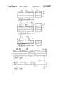
- FIGS. 1A-1C of the accompanying drawingsA known method of fabricating a wafer probe is illustrated in FIGS. 1A-1C of the accompanying drawings.
- a polyimide sheet 2(FIG. 1A) has a copper substrate 4 bonded to its back surface.
- a layer 6 of plate-up baseis deposited over the front surface 8 of sheet 2 by electron beam evaporation.
- Layer 6may comprise successive films of titanium, palladium and gold.
- Layer 6is patterned and a layer of gold is deposited electrolytically on the portions of layer 6 that remain, forming contact bases 8 and signal runs 10.
- a thick layer 14 (FIG. 1B) of photoresistis deposited over the surface of sheet 2 and is exposed to actinic radiation in accordance with the pattern of contact bases 8.
- the photoresistis developed and the resist that was exposed is removed, forming holes 16 through which the contact bases are exposed.
- Nickelis deposited electrolytically into holes 16 to form contact bumps 18 (FIG. 1C) bonded to contact bases 8, and the photoresist is stripped.
- the copper substrateis thinned, and is then patterned and etched to the configuration desired for a ground plane.
- the fabrication process described with reference to FIGS. 1A-1Cis subject to disadvantage. Since layer 14 is quite thick, it is difficult to ensure that all photoresist overlying contact bases 8 is removed after exposure and development of the photoresist, and consequently the nickel contact bumps normally do not contact the entire area of their respective gold contact bases. Consequently, the strength of the bond between the contact bumps and the respective contact bases is impaired.
- the holes formed in layer 14do not have vertical sides, and therefore the bodies of nickel that are deposited into the holes to form the contact bumps are not cylindrical but tend to have a mushroom configuration and to be non uniform in height.
- the bumpsare ground to a uniform height when the ground plane is in engagement with a planar back-up member. This grinding imposes stresses on the bumps, and frequently the bumps are broken from their contact bases, particularly because of the poor adhesion between the bumps and their bases.
- a contact elementis formed on a sheet of dielectric material by depositing conductive material in an opening in a first layer of dielectric material, and depositing a second layer of dielectric material over the first layer and over the conductive material in the opening. Material of the first layer is removed from the surface farther from the second layer so that the conductive material projects beyond the first layer.
- FIGS. 1A-1Cshow various steps in a known method of fabricating a wafer probe
- FIGS. 2A-2Fshow various steps of a method in accordance with the present invention.
- FIG. 2Aillustrates a sheet 50 of polyimide bonded to a substrate 52 of stainless steel.
- Sheet 50is about 25 ⁇ m thick.
- a layer 54 of aluminumis deposited over the upper surface 56 of layer 50 and is selectively etched using conventional techniques to form holes 58.
- the structureis then subjected to a reactive ion etching process, which may be carried out in a March Instruments Jupiter II reactive ion etcher, to remove polyimide exposed through holes 58.
- the pressure in the etcherdetermines whether the polyimide will be removed isotropically or anisotropically.
- the pressureis adjusted so that the etcher operates at the inflection on the transition between anisotropic and isotropic operation. This was found to be a pressure of 0.64 torr. At this pressure, the polyimide is etched isotropically, resulting in formation of downwardly tapering holes 60 (FIG. 2B) in sheet 50.
- the remaining aluminumis then removed using an aluminum etchant, and the structure is placed in a nickel plating bath with substrate 52 connected as cathode.
- Bodies 66(FIG. 2C) of nickel are electrolytically deposited in holes 60.
- Platingcontinues for a time that is selected to be sufficient to fill holes 60.
- a layer 68 of plate-up baseis deposited by electron beam evaporation over surface 56 of sheet 50.
- the plate-up basemay comprise consecutive films of titanium, palladium and gold. However, it is preferred that the plate-up base comprise consecutive films of chromium and gold.
- chemical and/or thermal bondingoccurs between layer 68 and surface 56. Good metal-to-metal adhesion is obtained between layer 68 and bodies 66.
- Layer 68is then selectively etched (FIG. 2D) so as to remove material of layer 68 except from bodies 66 and where signal runs connected to bodies 66 are required.
- the resulting structureis placed in a gold plating bath with substrate 52 connected as cathode, and gold is deposited electrolytically onto the remaining portions of layer 68 to form signal runs 70.
- a layer 72 of polyimideis then applied over surface 56 and signal runs 70 and is cured.
- the sequence of operations described with reference to FIGS. 2A-2Cis then repeated, except that the holes 76 (FIG. 2E) formed in polyimide layer 72 are positioned over the outer ends of signal runs 70 and the nickel plating step is omitted so that plate-up base 74 is deposited over the upper surface of layer 72 and into holes 76 and contacts signal runs 70.
- the tapered configuration of holes 76avoids step coverage problems with layer 74.
- a layer of photoresistis deposited over layer 74 and is exposed in accordance with a pattern that includes a ring extending around each hole 76.
- the photoresistis developed, and the unexposed photoresist is stripped, leaving a ring 80 of photoresist around each hole.
- the structureis placed in a gold plating bath with substrate 52 connected as a cathode, and a layer 82 of gold is deposited over the exposed plate-up base.
- Layer 82comprises interconnect portions 82a surrounded by the rings of photoresist and extending into holes 76 and a ground plane portion 82b.
- Photoresist rings 80are then removed, and the plate-up base that is exposed is removed by conventional selective etching techniques, thereby electrically isolating interconnect areas 82a and ground plane portion 82b (FIG. 2F).
- Substrate 52is then selectively etched so as to remove substrate 52 except for a narrow margin 86 around the periphery of sheet 50.
- the exposed lower surface of sheet 50is exposed to a reactive ion etching operation, so that the polyimide is etched back and bodies 66 in holes 60 then project beyond the lower surface of sheet 50, forming contact bumps.
- the device shown in FIG. 2Fis used to probe an integrated circuit in wafer form.
- the wafer probeis placed over the wafer, with the contact bumps registering with connection pads of a circuit under test, and the contact bumps are pressed into contact with the connection pads.
- Contact forceis provided by a body of elastomer material engaging the upper surface of the wafer probe.
- the vertical heights of the bodies of nickelwill not be equal.
- the nickel bodiesare ground while the upper surface of the wafer probe is supported by a planar back-up member.
- the wafer probe fabricated by the method described with reference to FIGS. 2A-2Fis superior to that fabricated by the method described with reference to FIG. 1, because the height of the bumps is controlled by the thickness of layer 50 and the amount of layer 50 that is removed by etching. Accordingly, there is very little variation in height of the bumps, and there is little need for grinding to bring the bumps to uniform height. Further, since plate-up base 68 is deposited directly onto surface 56 and body 66, superior adhesion is obtained between the nickel bumps and the plate-up base, so that if grinding should be necessary it less likely to result in any bumps being broken off.
- the configuration of the bumpsis controlled by the reactive ion etching, and it is possible to adjust the angle of the wedge by changing the pressure in the etcher.
Landscapes
- Physics & Mathematics (AREA)
- General Physics & Mathematics (AREA)
- Measuring Leads Or Probes (AREA)
- Testing Or Measuring Of Semiconductors Or The Like (AREA)
- Testing Of Individual Semiconductor Devices (AREA)
Abstract
Description
This invention relates to a method of fabricating a contact device.
It is known to test an integrated circuit having an array of connection pads at the wafer stage of fabrication, i.e., before dicing into separate chips, using a flexible wafer probe, comprising a sheet of polyimide having contact bumps projecting from one surface thereof in an array corresponding to the array of connection pads of the integrated circuit. The contact bumps are connected to a measurement instrument through strip-form signal lines deposited on the polyimide sheet.
A known method of fabricating a wafer probe is illustrated in FIGS. 1A-1C of the accompanying drawings. A polyimide sheet 2 (FIG. 1A) has acopper substrate 4 bonded to its back surface. Alayer 6 of plate-up base is deposited over thefront surface 8 ofsheet 2 by electron beam evaporation.Layer 6 may comprise successive films of titanium, palladium and gold.Layer 6 is patterned and a layer of gold is deposited electrolytically on the portions oflayer 6 that remain, formingcontact bases 8 and signal runs 10. A thick layer 14 (FIG. 1B) of photoresist is deposited over the surface ofsheet 2 and is exposed to actinic radiation in accordance with the pattern ofcontact bases 8. The photoresist is developed and the resist that was exposed is removed, formingholes 16 through which the contact bases are exposed. Nickel is deposited electrolytically intoholes 16 to form contact bumps 18 (FIG. 1C) bonded to contactbases 8, and the photoresist is stripped. The copper substrate is thinned, and is then patterned and etched to the configuration desired for a ground plane.
The fabrication process described with reference to FIGS. 1A-1C is subject to disadvantage. Sincelayer 14 is quite thick, it is difficult to ensure that all photoresist overlyingcontact bases 8 is removed after exposure and development of the photoresist, and consequently the nickel contact bumps normally do not contact the entire area of their respective gold contact bases. Consequently, the strength of the bond between the contact bumps and the respective contact bases is impaired. The holes formed inlayer 14 do not have vertical sides, and therefore the bodies of nickel that are deposited into the holes to form the contact bumps are not cylindrical but tend to have a mushroom configuration and to be non uniform in height. In order to ensure reliable contact between the bumps and the connection pads of the circuit under test, the bumps are ground to a uniform height when the ground plane is in engagement with a planar back-up member. This grinding imposes stresses on the bumps, and frequently the bumps are broken from their contact bases, particularly because of the poor adhesion between the bumps and their bases.
In accordance with the present invention, a contact element is formed on a sheet of dielectric material by depositing conductive material in an opening in a first layer of dielectric material, and depositing a second layer of dielectric material over the first layer and over the conductive material in the opening. Material of the first layer is removed from the surface farther from the second layer so that the conductive material projects beyond the first layer.
For a better understanding of the invention, and to show how the same may be carried into effect, reference will now be made, by way of example, to the accompanying drawings, in which:
FIGS. 1A-1C show various steps in a known method of fabricating a wafer probe, and
FIGS. 2A-2F show various steps of a method in accordance with the present invention.
FIG. 2A illustrates asheet 50 of polyimide bonded to asubstrate 52 of stainless steel.Sheet 50 is about 25 μm thick. Alayer 54 of aluminum is deposited over theupper surface 56 oflayer 50 and is selectively etched using conventional techniques to formholes 58. The structure is then subjected to a reactive ion etching process, which may be carried out in a March Instruments Jupiter II reactive ion etcher, to remove polyimide exposed throughholes 58. The pressure in the etcher determines whether the polyimide will be removed isotropically or anisotropically. Preferably, the pressure is adjusted so that the etcher operates at the inflection on the transition between anisotropic and isotropic operation. This was found to be a pressure of 0.64 torr. At this pressure, the polyimide is etched isotropically, resulting in formation of downwardly tapering holes 60 (FIG. 2B) insheet 50.
The remaining aluminum is then removed using an aluminum etchant, and the structure is placed in a nickel plating bath withsubstrate 52 connected as cathode. Bodies 66 (FIG. 2C) of nickel are electrolytically deposited inholes 60. Plating continues for a time that is selected to be sufficient to fillholes 60. Alayer 68 of plate-up base is deposited by electron beam evaporation oversurface 56 ofsheet 50. The plate-up base may comprise consecutive films of titanium, palladium and gold. However, it is preferred that the plate-up base comprise consecutive films of chromium and gold. Depending on the nature oflayer 68, chemical and/or thermal bonding occurs betweenlayer 68 andsurface 56. Good metal-to-metal adhesion is obtained betweenlayer 68 andbodies 66.Layer 68 is then selectively etched (FIG. 2D) so as to remove material oflayer 68 except frombodies 66 and where signal runs connected tobodies 66 are required. The resulting structure is placed in a gold plating bath withsubstrate 52 connected as cathode, and gold is deposited electrolytically onto the remaining portions oflayer 68 to form signal runs 70.
Alayer 72 of polyimide is then applied oversurface 56 and signal runs 70 and is cured. The sequence of operations described with reference to FIGS. 2A-2C is then repeated, except that the holes 76 (FIG. 2E) formed inpolyimide layer 72 are positioned over the outer ends ofsignal runs 70 and the nickel plating step is omitted so that plate-up base 74 is deposited over the upper surface oflayer 72 and intoholes 76 and contacts signal runs 70. The tapered configuration ofholes 76 avoids step coverage problems withlayer 74. A layer of photoresist is deposited overlayer 74 and is exposed in accordance with a pattern that includes a ring extending around eachhole 76. The photoresist is developed, and the unexposed photoresist is stripped, leaving aring 80 of photoresist around each hole. The structure is placed in a gold plating bath withsubstrate 52 connected as a cathode, and alayer 82 of gold is deposited over the exposed plate-up base.Layer 82 comprisesinterconnect portions 82a surrounded by the rings of photoresist and extending intoholes 76 and aground plane portion 82b. Photoresist rings 80 are then removed, and the plate-up base that is exposed is removed by conventional selective etching techniques, thereby electrically isolatinginterconnect areas 82a andground plane portion 82b (FIG. 2F).
The device shown in FIG. 2F is used to probe an integrated circuit in wafer form. The wafer probe is placed over the wafer, with the contact bumps registering with connection pads of a circuit under test, and the contact bumps are pressed into contact with the connection pads. Contact force is provided by a body of elastomer material engaging the upper surface of the wafer probe.
There is a possibility that the vertical heights of the bodies of nickel will not be equal. In order to ensure reliable contact between the contact bumps and the respective connection pads, the nickel bodies are ground while the upper surface of the wafer probe is supported by a planar back-up member.
The wafer probe fabricated by the method described with reference to FIGS. 2A-2F is superior to that fabricated by the method described with reference to FIG. 1, because the height of the bumps is controlled by the thickness oflayer 50 and the amount oflayer 50 that is removed by etching. Accordingly, there is very little variation in height of the bumps, and there is little need for grinding to bring the bumps to uniform height. Further, since plate-up base 68 is deposited directly ontosurface 56 andbody 66, superior adhesion is obtained between the nickel bumps and the plate-up base, so that if grinding should be necessary it less likely to result in any bumps being broken off. The configuration of the bumps is controlled by the reactive ion etching, and it is possible to adjust the angle of the wedge by changing the pressure in the etcher.
It will be appreciated that the invention is not restricted to the particular embodiment that has been described, and that variations may be made therein without departing from the scope of the invention as defined in the appended claims and equivalents thereof.
Claims (6)
1. A method of fabricating a contact element on a sheet of dielectric material, comprising:
(a) providing a first layer of dielectric material having first and second opposite surfaces and at least one opening,
(b) depositing conductive material in said opening,
(c) depositing a second layer of dielectric material over the first surface of the first layer and over the conductive material in said opening, and
(d) removing material of the first layer from its second surface so that the conductive material projects beyond the first layer.
2. A method according to claim 1, wherein step (a) comprises providing a layer of dielectric material, masking a surface of the layer of dielectric material with a mask formed with an opening, and removing material of the layer of dielectric material through the opening in the mask.
3. A method according to claim 2, comprising removing material of the layer of dielectric material by etching.
4. A method according to claim 3, comprising etching under conditions such that the dielectric material is removed isotropically.
5. A method according to claim 1, comprising, between steps (b) and (c), depositing a layer of conductive material over the first surface of the first layer and patterning the layer of conductive material to define portions that are in adhesive relationship with the conductive material in the opening.
6. A method according to claim 1, wherein the layer provided in step (a) is bonded at its second surface to a metal substrate, and the method comprises, between steps (c) and (d), removing the metal of the substrate so as to expose the second surface of the first layer of dielectric material.
Priority Applications (3)
| Application Number | Priority Date | Filing Date | Title |
|---|---|---|---|
| US07/424,467US4963225A (en) | 1989-10-20 | 1989-10-20 | Method of fabricating a contact device |
| EP19900311340EP0424105A3 (en) | 1989-10-20 | 1990-10-17 | Method of fabricating a contact device |
| JP2283264AJPH03179760A (en) | 1989-10-20 | 1990-10-19 | Contact element manufacturing method |
Applications Claiming Priority (1)
| Application Number | Priority Date | Filing Date | Title |
|---|---|---|---|
| US07/424,467US4963225A (en) | 1989-10-20 | 1989-10-20 | Method of fabricating a contact device |
Publications (1)
| Publication Number | Publication Date |
|---|---|
| US4963225Atrue US4963225A (en) | 1990-10-16 |
Family
ID=23682724
Family Applications (1)
| Application Number | Title | Priority Date | Filing Date |
|---|---|---|---|
| US07/424,467Expired - Fee RelatedUS4963225A (en) | 1989-10-20 | 1989-10-20 | Method of fabricating a contact device |
Country Status (3)
| Country | Link |
|---|---|
| US (1) | US4963225A (en) |
| EP (1) | EP0424105A3 (en) |
| JP (1) | JPH03179760A (en) |
Cited By (28)
| Publication number | Priority date | Publication date | Assignee | Title |
|---|---|---|---|---|
| US5177439A (en)* | 1991-08-30 | 1993-01-05 | U.S. Philips Corporation | Probe card for testing unencapsulated semiconductor devices |
| US5239260A (en)* | 1991-06-28 | 1993-08-24 | Digital Equipment Corporation | Semiconductor probe and alignment system |
| US5483741A (en)* | 1993-09-03 | 1996-01-16 | Micron Technology, Inc. | Method for fabricating a self limiting silicon based interconnect for testing bare semiconductor dice |
| US5495179A (en)* | 1991-06-04 | 1996-02-27 | Micron Technology, Inc. | Carrier having interchangeable substrate used for testing of semiconductor dies |
| US5523697A (en)* | 1993-09-03 | 1996-06-04 | Micron Technology, Inc. | Testing apparatus for engaging electrically conductive test pads on a semiconductor substrate having integrated circuitry for operability testing thereof |
| US5541525A (en)* | 1991-06-04 | 1996-07-30 | Micron Technology, Inc. | Carrier for testing an unpackaged semiconductor die |
| US5585282A (en)* | 1991-06-04 | 1996-12-17 | Micron Technology, Inc. | Process for forming a raised portion on a projecting contact for electrical testing of a semiconductor |
| US5626971A (en)* | 1994-12-28 | 1997-05-06 | Shi; Shei-Kung | Thin film probe |
| US5634267A (en)* | 1991-06-04 | 1997-06-03 | Micron Technology, Inc. | Method and apparatus for manufacturing known good semiconductor die |
| US5725787A (en)* | 1992-04-10 | 1998-03-10 | Candescent Technologies Corporation | Fabrication of light-emitting device with raised black matrix for use in optical devices such as flat-panel cathode-ray tubes |
| US5747358A (en)* | 1996-05-29 | 1998-05-05 | W. L. Gore & Associates, Inc. | Method of forming raised metallic contacts on electrical circuits |
| US5766979A (en)* | 1996-11-08 | 1998-06-16 | W. L. Gore & Associates, Inc. | Wafer level contact sheet and method of assembly |
| US5830565A (en)* | 1996-11-08 | 1998-11-03 | W. L. Gore & Associates, Inc. | High planarity and low thermal coefficient of expansion base for semi-conductor reliability screening |
| US5849633A (en)* | 1994-03-07 | 1998-12-15 | Micron Technology, Inc. | Electrically conductive projections and semiconductor processing method of forming same |
| US5865930A (en)* | 1992-04-10 | 1999-02-02 | Candescent Technologies Corporation | Formations of spacers suitable for use in flat panel displays |
| US5886535A (en)* | 1996-11-08 | 1999-03-23 | W. L. Gore & Associates, Inc. | Wafer level burn-in base unit substrate and assembly |
| US5896038A (en)* | 1996-11-08 | 1999-04-20 | W. L. Gore & Associates, Inc. | Method of wafer level burn-in |
| US5898311A (en)* | 1996-12-06 | 1999-04-27 | International Business Machines Corporation | Shorting pad having a flexible conductive sheet |
| US5909123A (en)* | 1996-11-08 | 1999-06-01 | W. L. Gore & Associates, Inc. | Method for performing reliability screening and burn-in of semi-conductor wafers |
| US5966022A (en)* | 1996-11-08 | 1999-10-12 | W. L. Gore & Associates, Inc. | Wafer level burn-in system |
| US5966593A (en)* | 1996-11-08 | 1999-10-12 | W. L. Gore & Associates, Inc. | Method of forming a wafer level contact sheet having a permanent z-axis material |
| WO2000019215A1 (en)* | 1998-09-30 | 2000-04-06 | Credence Systems Corporation | Thermal isolation plate for probe card |
| US6219908B1 (en) | 1991-06-04 | 2001-04-24 | Micron Technology, Inc. | Method and apparatus for manufacturing known good semiconductor die |
| US6340894B1 (en) | 1991-06-04 | 2002-01-22 | Micron Technology, Inc. | Semiconductor testing apparatus including substrate with contact members and conductive polymer interconnect |
| US20030218151A1 (en)* | 2001-12-04 | 2003-11-27 | Mark Akselrod | Aluminum oxide material for optical data storage |
| US6763578B2 (en) | 1988-09-30 | 2004-07-20 | Micron Technology, Inc. | Method and apparatus for manufacturing known good semiconductor die |
| US6828812B2 (en)* | 1991-06-04 | 2004-12-07 | Micron Technology, Inc. | Test apparatus for testing semiconductor dice including substrate with penetration limiting contacts for making electrical connections |
| EP2186132A4 (en)* | 2007-08-15 | 2018-01-03 | Tessera, Inc. | Interconnection element with posts formed by plating |
Families Citing this family (2)
| Publication number | Priority date | Publication date | Assignee | Title |
|---|---|---|---|---|
| JPH07105420B2 (en)* | 1991-08-26 | 1995-11-13 | ヒューズ・エアクラフト・カンパニー | Electrical connection with molded contacts |
| TWI287634B (en)* | 2004-12-31 | 2007-10-01 | Wen-Chang Dung | Micro-electromechanical probe circuit film, method for making the same and applications thereof |
Citations (5)
| Publication number | Priority date | Publication date | Assignee | Title |
|---|---|---|---|---|
| US3838984A (en)* | 1973-04-16 | 1974-10-01 | Sperry Rand Corp | Flexible carrier and interconnect for uncased ic chips |
| US4585991A (en)* | 1982-06-03 | 1986-04-29 | Texas Instruments Incorporated | Solid state multiprobe testing apparatus |
| US4676864A (en)* | 1985-05-15 | 1987-06-30 | Matsushita Electric Industrial Co., Ltd. | Bonding method of semiconductor device |
| US4740700A (en)* | 1986-09-02 | 1988-04-26 | Hughes Aircraft Company | Thermally insulative and electrically conductive interconnect and process for making same |
| US4878990A (en)* | 1988-05-23 | 1989-11-07 | General Dynamics Corp., Pomona Division | Electroformed and chemical milled bumped tape process |
Family Cites Families (3)
| Publication number | Priority date | Publication date | Assignee | Title |
|---|---|---|---|---|
| JPS54148484A (en)* | 1978-05-15 | 1979-11-20 | Nec Corp | Manufacture of semiconductor wafer test device |
| JPH0817192B2 (en)* | 1988-05-30 | 1996-02-21 | 株式会社日立製作所 | Method for manufacturing probe head for semiconductor LSI inspection device |
| JPH0680713B2 (en)* | 1989-10-11 | 1994-10-12 | 三菱電機株式会社 | Wafer test probe card and method of manufacturing the same |
- 1989
- 1989-10-20USUS07/424,467patent/US4963225A/ennot_activeExpired - Fee Related
- 1990
- 1990-10-17EPEP19900311340patent/EP0424105A3/ennot_activeWithdrawn
- 1990-10-19JPJP2283264Apatent/JPH03179760A/enactivePending
Patent Citations (5)
| Publication number | Priority date | Publication date | Assignee | Title |
|---|---|---|---|---|
| US3838984A (en)* | 1973-04-16 | 1974-10-01 | Sperry Rand Corp | Flexible carrier and interconnect for uncased ic chips |
| US4585991A (en)* | 1982-06-03 | 1986-04-29 | Texas Instruments Incorporated | Solid state multiprobe testing apparatus |
| US4676864A (en)* | 1985-05-15 | 1987-06-30 | Matsushita Electric Industrial Co., Ltd. | Bonding method of semiconductor device |
| US4740700A (en)* | 1986-09-02 | 1988-04-26 | Hughes Aircraft Company | Thermally insulative and electrically conductive interconnect and process for making same |
| US4878990A (en)* | 1988-05-23 | 1989-11-07 | General Dynamics Corp., Pomona Division | Electroformed and chemical milled bumped tape process |
Cited By (64)
| Publication number | Priority date | Publication date | Assignee | Title |
|---|---|---|---|---|
| US6489718B1 (en) | 1982-04-10 | 2002-12-03 | Candescent Technologies Corporation | Spacer suitable for use in flat panel display |
| US6763578B2 (en) | 1988-09-30 | 2004-07-20 | Micron Technology, Inc. | Method and apparatus for manufacturing known good semiconductor die |
| US5495179A (en)* | 1991-06-04 | 1996-02-27 | Micron Technology, Inc. | Carrier having interchangeable substrate used for testing of semiconductor dies |
| US6983536B2 (en) | 1991-06-04 | 2006-01-10 | Micron Technology, Inc. | Method and apparatus for manufacturing known good semiconductor die |
| US6340894B1 (en) | 1991-06-04 | 2002-01-22 | Micron Technology, Inc. | Semiconductor testing apparatus including substrate with contact members and conductive polymer interconnect |
| US5541525A (en)* | 1991-06-04 | 1996-07-30 | Micron Technology, Inc. | Carrier for testing an unpackaged semiconductor die |
| US5585282A (en)* | 1991-06-04 | 1996-12-17 | Micron Technology, Inc. | Process for forming a raised portion on a projecting contact for electrical testing of a semiconductor |
| US6219908B1 (en) | 1991-06-04 | 2001-04-24 | Micron Technology, Inc. | Method and apparatus for manufacturing known good semiconductor die |
| US5634267A (en)* | 1991-06-04 | 1997-06-03 | Micron Technology, Inc. | Method and apparatus for manufacturing known good semiconductor die |
| US20040214409A1 (en)* | 1991-06-04 | 2004-10-28 | Warren Farnworth | Method and apparatus for manufacturing known good semiconductor die |
| US6828812B2 (en)* | 1991-06-04 | 2004-12-07 | Micron Technology, Inc. | Test apparatus for testing semiconductor dice including substrate with penetration limiting contacts for making electrical connections |
| US5239260A (en)* | 1991-06-28 | 1993-08-24 | Digital Equipment Corporation | Semiconductor probe and alignment system |
| US5177439A (en)* | 1991-08-30 | 1993-01-05 | U.S. Philips Corporation | Probe card for testing unencapsulated semiconductor devices |
| US5725787A (en)* | 1992-04-10 | 1998-03-10 | Candescent Technologies Corporation | Fabrication of light-emitting device with raised black matrix for use in optical devices such as flat-panel cathode-ray tubes |
| US5985067A (en)* | 1992-04-10 | 1999-11-16 | Candescent Technologies Corporation | Formation of spacers suitable for use in flat panel displays |
| US5865930A (en)* | 1992-04-10 | 1999-02-02 | Candescent Technologies Corporation | Formations of spacers suitable for use in flat panel displays |
| US6157123A (en)* | 1992-04-10 | 2000-12-05 | Candescent Technologies Corporation | Flat panel display typically having transition metal oxide in ceramic core or/and resistive skin of spacer |
| US6670819B2 (en) | 1993-09-03 | 2003-12-30 | Micron Technology, Inc. | Methods of engaging electrically conductive pads on a semiconductor substrate |
| US6124721A (en)* | 1993-09-03 | 2000-09-26 | Micron Technology, Inc. | Method of engaging electrically conductive test pads on a semiconductor substrate |
| US20040207421A1 (en)* | 1993-09-03 | 2004-10-21 | Farnworth Warren M. | Method and apparatus for testing semiconductor circuitry for operability and method of forming apparatus for testing semiconductor circuitry for operability |
| US20040174178A1 (en)* | 1993-09-03 | 2004-09-09 | Farnworth Warren M. | Method and apparatus for testing semiconductor circuitry for operability and method of forming apparatus for testing semiconductor circuitry for operability |
| US6462571B1 (en) | 1993-09-03 | 2002-10-08 | Micron Technology, Inc. | Engagement probes |
| US20040095158A1 (en)* | 1993-09-03 | 2004-05-20 | Farnworth Warren M. | Apparatuses configured to engage a conductive pad |
| US7098475B2 (en) | 1993-09-03 | 2006-08-29 | Micron Technology, Inc. | Apparatuses configured to engage a conductive pad |
| US20040021476A1 (en)* | 1993-09-03 | 2004-02-05 | Farnworth Warren M. | Method and apparatus for testing semiconductor circuitry for operability and method of forming apparatus for testing semiconductor circuitry for operability |
| US6686758B1 (en) | 1993-09-03 | 2004-02-03 | Micron Technology, Inc. | Engagement probe and apparatuses configured to engage a conductive pad |
| US6833727B2 (en) | 1993-09-03 | 2004-12-21 | Micron Technology, Inc. | Method and apparatus for testing semiconductor circuitry for operability and method of forming apparatus for testing semiconductor circuitry for operability |
| US6657450B2 (en) | 1993-09-03 | 2003-12-02 | Micron Technology, Inc. | Methods of engaging electrically conductive test pads on a semiconductor substrate removable electrical interconnect apparatuses, engagement probes and removable engagement probes |
| US7116118B2 (en) | 1993-09-03 | 2006-10-03 | Micron Technology, Inc. | Method and apparatus for testing semiconductor circuitry for operability and method of forming apparatus for testing semiconductor circuitry for operability |
| US6127195A (en)* | 1993-09-03 | 2000-10-03 | Micron Technology, Inc. | Methods of forming an apparatus for engaging electrically conductive pads and method of forming a removable electrical interconnect apparatus |
| US7026835B2 (en) | 1993-09-03 | 2006-04-11 | Micron Technology, Inc. | Engagement probe having a grouping of projecting apexes for engaging a conductive pad |
| US7330036B2 (en) | 1993-09-03 | 2008-02-12 | Micron Technology, Inc. | Engagement Probes |
| US6614249B1 (en) | 1993-09-03 | 2003-09-02 | Micron Technology, Inc. | Methods of forming apparatuses and a method of engaging electrically conductive test pads on a semiconductor substrate |
| US6573740B2 (en) | 1993-09-03 | 2003-06-03 | Micron Technology, Inc. | Method of forming an apparatus configured to engage an electrically conductive pad on a semiconductive substrate and a method of engaging electrically conductive pads on a semiconductive substrate |
| US5523697A (en)* | 1993-09-03 | 1996-06-04 | Micron Technology, Inc. | Testing apparatus for engaging electrically conductive test pads on a semiconductor substrate having integrated circuitry for operability testing thereof |
| US5483741A (en)* | 1993-09-03 | 1996-01-16 | Micron Technology, Inc. | Method for fabricating a self limiting silicon based interconnect for testing bare semiconductor dice |
| US6380754B1 (en) | 1993-09-03 | 2002-04-30 | Micron Technology, Inc. | Removable electrical interconnect apparatuses including an engagement proble |
| US6392426B2 (en) | 1993-09-03 | 2002-05-21 | Micron Technology, Inc. | Methods of forming apparatuses and a method of engaging electrically conductive test pads on a semiconductor substrate |
| US5869787A (en)* | 1994-03-07 | 1999-02-09 | Micron Technology, Inc. | Electrically conductive projections |
| US5849633A (en)* | 1994-03-07 | 1998-12-15 | Micron Technology, Inc. | Electrically conductive projections and semiconductor processing method of forming same |
| US6255213B1 (en) | 1994-03-07 | 2001-07-03 | Micron Technology, Inc. | Method of forming a structure upon a semiconductive substrate |
| US6248962B1 (en) | 1994-03-07 | 2001-06-19 | Micron Technology, Inc. | Electrically conductive projections of the same material as their substrate |
| US6093643A (en)* | 1994-03-07 | 2000-07-25 | Micron Technology, Inc. | Electrically conductive projections and semiconductor processing method of forming same |
| US6441320B2 (en) | 1994-03-07 | 2002-08-27 | Micron Technology, Inc. | Electrically conductive projections having conductive coverings |
| US5626971A (en)* | 1994-12-28 | 1997-05-06 | Shi; Shei-Kung | Thin film probe |
| US5786270A (en)* | 1996-05-29 | 1998-07-28 | W. L. Gore & Associates, Inc. | Method of forming raised metallic contacts on electrical circuits for permanent bonding |
| US5747358A (en)* | 1996-05-29 | 1998-05-05 | W. L. Gore & Associates, Inc. | Method of forming raised metallic contacts on electrical circuits |
| US6046060A (en)* | 1996-11-08 | 2000-04-04 | W. L. Gore & Associates, Inc. | Method of making a high planarity, low CTE base for semiconductor reliability screening |
| US5766979A (en)* | 1996-11-08 | 1998-06-16 | W. L. Gore & Associates, Inc. | Wafer level contact sheet and method of assembly |
| US5966593A (en)* | 1996-11-08 | 1999-10-12 | W. L. Gore & Associates, Inc. | Method of forming a wafer level contact sheet having a permanent z-axis material |
| US5966022A (en)* | 1996-11-08 | 1999-10-12 | W. L. Gore & Associates, Inc. | Wafer level burn-in system |
| US5909123A (en)* | 1996-11-08 | 1999-06-01 | W. L. Gore & Associates, Inc. | Method for performing reliability screening and burn-in of semi-conductor wafers |
| US5896038A (en)* | 1996-11-08 | 1999-04-20 | W. L. Gore & Associates, Inc. | Method of wafer level burn-in |
| US5830565A (en)* | 1996-11-08 | 1998-11-03 | W. L. Gore & Associates, Inc. | High planarity and low thermal coefficient of expansion base for semi-conductor reliability screening |
| US5886535A (en)* | 1996-11-08 | 1999-03-23 | W. L. Gore & Associates, Inc. | Wafer level burn-in base unit substrate and assembly |
| US6313411B1 (en) | 1996-11-08 | 2001-11-06 | W. L. Gore & Associates, Inc. | Wafer level contact sheet and method of assembly |
| US5898311A (en)* | 1996-12-06 | 1999-04-27 | International Business Machines Corporation | Shorting pad having a flexible conductive sheet |
| US6081110A (en)* | 1998-09-30 | 2000-06-27 | Credence Systems Corporation | Thermal isolation plate for probe card |
| WO2000019215A1 (en)* | 1998-09-30 | 2000-04-06 | Credence Systems Corporation | Thermal isolation plate for probe card |
| US6846434B2 (en) | 2001-12-04 | 2005-01-25 | Landauer, Inc. | Aluminum oxide material for optical data storage |
| US6811607B2 (en) | 2001-12-04 | 2004-11-02 | Landauer, Inc. | Method for forming aluminum oxide material used in optical data storage |
| US20040069210A1 (en)* | 2001-12-04 | 2004-04-15 | Mark Akselrod | Method for forming aluminum oxide material used in optical data storage |
| US20030218151A1 (en)* | 2001-12-04 | 2003-11-27 | Mark Akselrod | Aluminum oxide material for optical data storage |
| EP2186132A4 (en)* | 2007-08-15 | 2018-01-03 | Tessera, Inc. | Interconnection element with posts formed by plating |
Also Published As
| Publication number | Publication date |
|---|---|
| EP0424105A2 (en) | 1991-04-24 |
| JPH03179760A (en) | 1991-08-05 |
| EP0424105A3 (en) | 1992-02-26 |
Similar Documents
| Publication | Publication Date | Title |
|---|---|---|
| US4963225A (en) | Method of fabricating a contact device | |
| US5633122A (en) | Test fixture and method for producing a test fixture for testing unpackaged semiconductor die | |
| US5926029A (en) | Ultra fine probe contacts | |
| US6222280B1 (en) | Test interconnect for semiconductor components having bumped and planar contacts | |
| US5723347A (en) | Semi-conductor chip test probe and process for manufacturing the probe | |
| US4617730A (en) | Method of fabricating a chip interposer | |
| US6314641B1 (en) | Interconnect for testing semiconductor components and method of fabrication | |
| US6018249A (en) | Test system with mechanical alignment for semiconductor chip scale packages and dice | |
| US6285203B1 (en) | Test system having alignment member for aligning semiconductor components | |
| US6265246B1 (en) | Microcap wafer-level package | |
| WO1994017548A1 (en) | Method for forming deep conductive feedthroughs and an interconnect layer that includes feedthroughs formed in accordance with the method | |
| EP0145862B1 (en) | Metallization of a ceramic substrate | |
| US5030318A (en) | Method of making electrical probe diaphragms | |
| KR20090005230A (en) | Method for forming microelectronic spring structures on a substrate | |
| US5118584A (en) | Method of producing microbump circuits for flip chip mounting | |
| US4466181A (en) | Method for mounting conjoined devices | |
| US6969681B2 (en) | Method for fabricating a semiconductor component using contact printing | |
| KR100807426B1 (en) | Interconnect Assemblies and Methods | |
| US6819127B1 (en) | Method for testing semiconductor components using interposer | |
| US6667627B2 (en) | Probe for inspecting semiconductor device and method of manufacturing the same | |
| US7011986B2 (en) | Method for manufacturing a housing for a chip with a micromechanical structure | |
| JP3446607B2 (en) | Method of manufacturing contact pin and contact probe | |
| KR100464681B1 (en) | Method for manufacturing tip of electric contactor for testing electro device | |
| JP4077666B2 (en) | Contact probe manufacturing method | |
| JP3003344B2 (en) | Method of forming bump electrodes |
Legal Events
| Date | Code | Title | Description |
|---|---|---|---|
| AS | Assignment | Owner name:TEKTRONIX, INC., 14150 S.W. KARL BRAUN DRIVE, P.O. Free format text:ASSIGNMENT OF ASSIGNORS INTEREST.;ASSIGNOR:LEHMAN-LAMER, GAIL R.;REEL/FRAME:005392/0228 Effective date:19891020 | |
| FEPP | Fee payment procedure | Free format text:PAYOR NUMBER ASSIGNED (ORIGINAL EVENT CODE: ASPN); ENTITY STATUS OF PATENT OWNER: LARGE ENTITY | |
| FPAY | Fee payment | Year of fee payment:4 | |
| FPAY | Fee payment | Year of fee payment:8 | |
| REMI | Maintenance fee reminder mailed | ||
| LAPS | Lapse for failure to pay maintenance fees | ||
| STCH | Information on status: patent discontinuation | Free format text:PATENT EXPIRED DUE TO NONPAYMENT OF MAINTENANCE FEES UNDER 37 CFR 1.362 | |
| FP | Lapsed due to failure to pay maintenance fee | Effective date:20021016 |