US4962063A - Multistep planarized chemical vapor deposition process with the use of low melting inorganic material for flowing while depositing - Google Patents
Multistep planarized chemical vapor deposition process with the use of low melting inorganic material for flowing while depositingDownload PDFInfo
- Publication number
- US4962063A US4962063AUS07/321,943US32194389AUS4962063AUS 4962063 AUS4962063 AUS 4962063AUS 32194389 AUS32194389 AUS 32194389AUS 4962063 AUS4962063 AUS 4962063A
- Authority
- US
- United States
- Prior art keywords
- layer
- depositing
- integrated circuit
- low melting
- circuit structure
- Prior art date
- Legal status (The legal status is an assumption and is not a legal conclusion. Google has not performed a legal analysis and makes no representation as to the accuracy of the status listed.)
- Expired - Fee Related
Links
Images


Classifications
- H—ELECTRICITY
- H01—ELECTRIC ELEMENTS
- H01L—SEMICONDUCTOR DEVICES NOT COVERED BY CLASS H10
- H01L21/00—Processes or apparatus adapted for the manufacture or treatment of semiconductor or solid state devices or of parts thereof
- H01L21/02—Manufacture or treatment of semiconductor devices or of parts thereof
- H01L21/02104—Forming layers
- H01L21/02107—Forming insulating materials on a substrate
- H01L21/02109—Forming insulating materials on a substrate characterised by the type of layer, e.g. type of material, porous/non-porous, pre-cursors, mixtures or laminates
- H01L21/02112—Forming insulating materials on a substrate characterised by the type of layer, e.g. type of material, porous/non-porous, pre-cursors, mixtures or laminates characterised by the material of the layer
- H01L21/02123—Forming insulating materials on a substrate characterised by the type of layer, e.g. type of material, porous/non-porous, pre-cursors, mixtures or laminates characterised by the material of the layer the material containing silicon
- H01L21/02126—Forming insulating materials on a substrate characterised by the type of layer, e.g. type of material, porous/non-porous, pre-cursors, mixtures or laminates characterised by the material of the layer the material containing silicon the material containing Si, O, and at least one of H, N, C, F, or other non-metal elements, e.g. SiOC, SiOC:H or SiONC
- H01L21/02129—Forming insulating materials on a substrate characterised by the type of layer, e.g. type of material, porous/non-porous, pre-cursors, mixtures or laminates characterised by the material of the layer the material containing silicon the material containing Si, O, and at least one of H, N, C, F, or other non-metal elements, e.g. SiOC, SiOC:H or SiONC the material being boron or phosphorus doped silicon oxides, e.g. BPSG, BSG or PSG
- H—ELECTRICITY
- H01—ELECTRIC ELEMENTS
- H01L—SEMICONDUCTOR DEVICES NOT COVERED BY CLASS H10
- H01L21/00—Processes or apparatus adapted for the manufacture or treatment of semiconductor or solid state devices or of parts thereof
- H01L21/02—Manufacture or treatment of semiconductor devices or of parts thereof
- H01L21/02104—Forming layers
- H01L21/02107—Forming insulating materials on a substrate
- H01L21/02109—Forming insulating materials on a substrate characterised by the type of layer, e.g. type of material, porous/non-porous, pre-cursors, mixtures or laminates
- H01L21/022—Forming insulating materials on a substrate characterised by the type of layer, e.g. type of material, porous/non-porous, pre-cursors, mixtures or laminates the layer being a laminate, i.e. composed of sublayers, e.g. stacks of alternating high-k metal oxides
- H—ELECTRICITY
- H01—ELECTRIC ELEMENTS
- H01L—SEMICONDUCTOR DEVICES NOT COVERED BY CLASS H10
- H01L21/00—Processes or apparatus adapted for the manufacture or treatment of semiconductor or solid state devices or of parts thereof
- H01L21/02—Manufacture or treatment of semiconductor devices or of parts thereof
- H01L21/02104—Forming layers
- H01L21/02107—Forming insulating materials on a substrate
- H01L21/02225—Forming insulating materials on a substrate characterised by the process for the formation of the insulating layer
- H01L21/0226—Forming insulating materials on a substrate characterised by the process for the formation of the insulating layer formation by a deposition process
- H01L21/02263—Forming insulating materials on a substrate characterised by the process for the formation of the insulating layer formation by a deposition process deposition from the gas or vapour phase
- H01L21/02271—Forming insulating materials on a substrate characterised by the process for the formation of the insulating layer formation by a deposition process deposition from the gas or vapour phase deposition by decomposition or reaction of gaseous or vapour phase compounds, i.e. chemical vapour deposition
- H—ELECTRICITY
- H01—ELECTRIC ELEMENTS
- H01L—SEMICONDUCTOR DEVICES NOT COVERED BY CLASS H10
- H01L21/00—Processes or apparatus adapted for the manufacture or treatment of semiconductor or solid state devices or of parts thereof
- H01L21/02—Manufacture or treatment of semiconductor devices or of parts thereof
- H01L21/04—Manufacture or treatment of semiconductor devices or of parts thereof the devices having potential barriers, e.g. a PN junction, depletion layer or carrier concentration layer
- H01L21/18—Manufacture or treatment of semiconductor devices or of parts thereof the devices having potential barriers, e.g. a PN junction, depletion layer or carrier concentration layer the devices having semiconductor bodies comprising elements of Group IV of the Periodic Table or AIIIBV compounds with or without impurities, e.g. doping materials
- H01L21/30—Treatment of semiconductor bodies using processes or apparatus not provided for in groups H01L21/20 - H01L21/26
- H01L21/31—Treatment of semiconductor bodies using processes or apparatus not provided for in groups H01L21/20 - H01L21/26 to form insulating layers thereon, e.g. for masking or by using photolithographic techniques; After treatment of these layers; Selection of materials for these layers
- H01L21/3105—After-treatment
- H01L21/31051—Planarisation of the insulating layers
- H01L21/31053—Planarisation of the insulating layers involving a dielectric removal step
- H01L21/31055—Planarisation of the insulating layers involving a dielectric removal step the removal being a chemical etching step, e.g. dry etching
- H—ELECTRICITY
- H01—ELECTRIC ELEMENTS
- H01L—SEMICONDUCTOR DEVICES NOT COVERED BY CLASS H10
- H01L21/00—Processes or apparatus adapted for the manufacture or treatment of semiconductor or solid state devices or of parts thereof
- H01L21/70—Manufacture or treatment of devices consisting of a plurality of solid state components formed in or on a common substrate or of parts thereof; Manufacture of integrated circuit devices or of parts thereof
- H01L21/71—Manufacture of specific parts of devices defined in group H01L21/70
- H01L21/768—Applying interconnections to be used for carrying current between separate components within a device comprising conductors and dielectrics
- H01L21/76801—Applying interconnections to be used for carrying current between separate components within a device comprising conductors and dielectrics characterised by the formation and the after-treatment of the dielectrics, e.g. smoothing
- H01L21/76819—Smoothing of the dielectric
- H—ELECTRICITY
- H01—ELECTRIC ELEMENTS
- H01L—SEMICONDUCTOR DEVICES NOT COVERED BY CLASS H10
- H01L21/00—Processes or apparatus adapted for the manufacture or treatment of semiconductor or solid state devices or of parts thereof
- H01L21/02—Manufacture or treatment of semiconductor devices or of parts thereof
- H01L21/02104—Forming layers
- H01L21/02107—Forming insulating materials on a substrate
- H01L21/02109—Forming insulating materials on a substrate characterised by the type of layer, e.g. type of material, porous/non-porous, pre-cursors, mixtures or laminates
- H01L21/02112—Forming insulating materials on a substrate characterised by the type of layer, e.g. type of material, porous/non-porous, pre-cursors, mixtures or laminates characterised by the material of the layer
- H01L21/02123—Forming insulating materials on a substrate characterised by the type of layer, e.g. type of material, porous/non-porous, pre-cursors, mixtures or laminates characterised by the material of the layer the material containing silicon
- H01L21/02164—Forming insulating materials on a substrate characterised by the type of layer, e.g. type of material, porous/non-porous, pre-cursors, mixtures or laminates characterised by the material of the layer the material containing silicon the material being a silicon oxide, e.g. SiO2
- H—ELECTRICITY
- H01—ELECTRIC ELEMENTS
- H01L—SEMICONDUCTOR DEVICES NOT COVERED BY CLASS H10
- H01L21/00—Processes or apparatus adapted for the manufacture or treatment of semiconductor or solid state devices or of parts thereof
- H01L21/02—Manufacture or treatment of semiconductor devices or of parts thereof
- H01L21/02104—Forming layers
- H01L21/02107—Forming insulating materials on a substrate
- H01L21/02225—Forming insulating materials on a substrate characterised by the process for the formation of the insulating layer
- H01L21/0226—Forming insulating materials on a substrate characterised by the process for the formation of the insulating layer formation by a deposition process
- H01L21/02263—Forming insulating materials on a substrate characterised by the process for the formation of the insulating layer formation by a deposition process deposition from the gas or vapour phase
- H01L21/02271—Forming insulating materials on a substrate characterised by the process for the formation of the insulating layer formation by a deposition process deposition from the gas or vapour phase deposition by decomposition or reaction of gaseous or vapour phase compounds, i.e. chemical vapour deposition
- H01L21/02274—Forming insulating materials on a substrate characterised by the process for the formation of the insulating layer formation by a deposition process deposition from the gas or vapour phase deposition by decomposition or reaction of gaseous or vapour phase compounds, i.e. chemical vapour deposition in the presence of a plasma [PECVD]
- Y—GENERAL TAGGING OF NEW TECHNOLOGICAL DEVELOPMENTS; GENERAL TAGGING OF CROSS-SECTIONAL TECHNOLOGIES SPANNING OVER SEVERAL SECTIONS OF THE IPC; TECHNICAL SUBJECTS COVERED BY FORMER USPC CROSS-REFERENCE ART COLLECTIONS [XRACs] AND DIGESTS
- Y10—TECHNICAL SUBJECTS COVERED BY FORMER USPC
- Y10S—TECHNICAL SUBJECTS COVERED BY FORMER USPC CROSS-REFERENCE ART COLLECTIONS [XRACs] AND DIGESTS
- Y10S148/00—Metal treatment
- Y10S148/133—Reflow oxides and glasses
- Y—GENERAL TAGGING OF NEW TECHNOLOGICAL DEVELOPMENTS; GENERAL TAGGING OF CROSS-SECTIONAL TECHNOLOGIES SPANNING OVER SEVERAL SECTIONS OF THE IPC; TECHNICAL SUBJECTS COVERED BY FORMER USPC CROSS-REFERENCE ART COLLECTIONS [XRACs] AND DIGESTS
- Y10—TECHNICAL SUBJECTS COVERED BY FORMER USPC
- Y10S—TECHNICAL SUBJECTS COVERED BY FORMER USPC CROSS-REFERENCE ART COLLECTIONS [XRACs] AND DIGESTS
- Y10S438/00—Semiconductor device manufacturing: process
- Y10S438/907—Continuous processing
- Y10S438/908—Utilizing cluster apparatus
Definitions
- This inventionrelates to a planarization process for integrated circuit structures. More particularly, this invention relates to a planarization process which utilizes an initial ECR plasma deposition to achieve a high density vertical deposition of a conformal insulation layer with a high aspect ratio; a low melting inorganic planarization material to planarize the ECR plasma deposited layer; and an optional CVD layer applied over the planarized ECR plasma layer.
- a layer of insulating materialsuch as silicon oxide is applied over such uneven surfaces, to permit the formation of further patterned layers thereover.
- silicon oxidetends to conform to the underlying topography resulting in the creation of a nonplanar or stepped surface. It is very difficult to pattern further layers over such an uneven surface using standard lithography techniques.
- planarizing layers of either photoresist or organic-based glass materialssuch as "SOG” (Spin On Glass) which will etch at about the same rate as the underlying silicon oxide insulating layer.
- SOGSpin On Glass
- the structureis then anisotropically etched to remove the planarizing layer, as well as raised portions of the underlying silicon oxide layer.
- both photoresist and SOGhave what is called a loading effect.
- the etch rate of these materialsdepends upon how much of the insulating layer, e.g., the silicon oxide layer, is exposed.
- achieving an equal etch rate of both insulating material (silicon oxide) and the sacrificial or planarizing materialis very difficult and the etch rate is, therefore, dependent upon the geometry of the structure.
- the spinning process of applying either of these two planarizing materialsis not effective.
- planarizing materialsalso have limited step coverage and are limited with respect to the total amount or thickness of these materials which can be deposited. Furthermore, since these planarizing materials are dispersed in organic binders and solvents, prior to application of such planarizing materials, the integrated circuit structure must be removed from a vacuum chamber in which the insulating layer such as silicon oxide is deposited, e.g., by CVD methods, in order to coat the structure with the planarizing layer. After such coating, the solvent in the planarizing coating must be allowed to evaporate and the planarizing coating must then be baked to remove further solvents and to harden the coating prior to the etching step, which is conventionally a dry etching process which is also usually carried out in a vacuum chamber.
- the initial conformal insulating layere.g. a layer of silicon oxide, which is conventionally applied over the underlying metal lines or other patterned layers using CVD deposition techniques, does not always adequately fill in those regions between closely spaced apart metal lines or other raised parts of the underlying integrated circuit structure. This can result in the formation of voids in those portions of the silicon oxide layer deposited between such closely spaced apart raised parts of the integrated circuit structure.
- ECRelectron cyclotron resonance
- the ECR plasma deposition process described in these publicationsprovides deposition of material via a plasma wherein a plasma formation chamber is surrounded by one or more magnetic coils to generate a magnetic field which produces an electron cyclotron resonance in the plasma formation chamber with the axis of the magnetic field extending toward a deposition chamber in a divergent manner.
- the resulting depositionfor example, of SiO 2 from oxygen and silane gases, is a more dense conformal insulating layer with a high aspect ratio to provide better filling of the regions between closely spaced apart lines, thus eliminating or at least mitigating the problem of void formation in the insulation material deposited in such areas.
- an object of this inventionto provide a process for planarizing an integrated circuit structure comprising an initial ECR plasma deposition of a conformal insulation layer followed by application thereto of a low melting inorganic planarizing material.
- It is another object of this invention to provide a process for planarizing an integrated circuit structurewhich comprises the steps of ECR plasma depositing a conformal insulating layer over an integrated circuit substrate followed by depositing a layer of a low melting inorganic planarizing material thereon, and then planarizing the structure by etching the inorganic planarizing layer.
- It is another object of this invention to provide a process for planarizing an integrated circuit structurewhich comprises the steps of ECR plasma depositing a conformal insulating layer over an integrated circuit substrate followed by depositing a layer of a low melting glass planarizing material thereon, and then planarizing the structure by dry etching the low melting glass planarizing layer.
- It is yet another object of this invention to provide a process for planarizing an integrated circuit structurewhich comprises the steps of ECR plasma depositing a conformal insulating layer over an integrated circuit substrate followed by depositing a layer of a low melting glass planarizing material thereon, and then anisotropically dry etching the low melting glass planarizing layer in an etching zone in the apparatus without exposing the coated structure to the ambient atmosphere.
- It is still another object of this invention to provide a process for planarizing an integrated circuit structurewhich comprises the steps of ECR plasma depositing a conformal insulating layer over an integrated circuit substrate followed by depositing a layer of a low melting glass planarizing material thereon, etching the low melting glass planarizing layer to remove at least some of the low melting inorganic planarizing material, and then depositing a further layer of an insulating material over the structure.
- It is a further object of this invention to provide a process for planarizing an integrated circuit structurewhich comprises the steps of ECR plasma depositing a conformal insulating layer over an integrated circuit substrate, depositing a layer of a low melting glass planarizing material thereon, etching the low melting glass planarizing layer to planarize the structure, and then CVD depositing a further layer of an insulating material over the structure.
- It is yet another object of this invention to provide apparatus for planarizing an integrated circuit structurewhich comprises means for ECR plasma depositing a conformal insulating layer over an integrated circuit substrate, means for depositing a layer of a low melting glass planarizing material thereon, means for anisotropically dry etching the low melting glass planarizing layer to planarize the structure, and means for then CVD depositing a further layer of an insulating material over the structure.
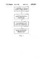
- FIG. 1is a flow sheet illustrating the process of the invention.
- FIG. 2is a fragmentary vertical cross-sectional view of an integrated circuit structure having patterned layers thereon and a conformal insulating layer formed thereover by ECR plasma deposition.
- FIG. 3is a fragmentary vertical cross-sectional view of the integrated circuit structure of FIG. 2 showing a planarizing layer of a low melting glass material deposited over the conformal insulating layer.
- FIG. 4is a fragmentary vertical cross-sectional view of the integrated circuit structure of FIG. 3 after planarization of the structure.
- FIG. 5is a fragmentary vertical cross-sectional view of the integrated circuit structure of FIG. 4 with a further layer of insulation material CVD deposited over the planarized structure.
- FIG. 6is a schematic view of apparatus which may be used in carrying out the process of the invention.
- an improved planarization processwherein over a patterned integrated circuit structure of a semiconductor wafer is first formed a conformal insulation layer deposited by ECR plasma deposition of an insulation material.
- the ECR plasma depositionis carried out until the trenches or low regions between adjacent high regions are completely filled with insulation material.
- a planarization layer of a low melting glass material, such as a boron oxide glass,is then formed over the integrated circuit structure to a depth or thickness sufficient to cover the highest portions of the ECR plasma deposited insulation layer.
- planarization layeris then anisotropically dry etched back to remove some or all of the planarization material, resulting in a planarized surface on the ECR plasma deposited insulation layer.
- An optional further layer of insulation materialmay then be conventionally CVD deposited over the planarized ECR plasma deposited insulation layer.
- the processmay be used for front end application such as dielectric planarization, for filling trenches or slots, or for top side planarization as well as the illustrated intermetal planarization.
- a phosphorus silicate glassPSG
- the processmay also be used to planarize an integrated circuit structure prior to a blanket deposit of another metal layer such as tungsten.
- raised portionsportions of an integrated circuit structure raised with respect to the height of the surface therebetween and thus may include not only structures raised with respect to the entire surface but also the raised sidewalls, for example, of a trench or slot with respect to the bottom of the trench.
- an integrated circuit structureis generally shown at 2 comprising a semiconductor wafer or substrate 10, such as, for example, a silicon substrate, having raised portions 14 thereon which may comprise, for example, metal lines or other conductive or insulating materials.
- a conformal insulation layer 20which may, for example, comprise a silicon oxide, a silicon oxynitride, or a silicon nitride layer, or a silicate such as phosphorus silicate when the underlying integrated circuit structure comprises silicon, is shown formed over substrate 10 and raised portions 14 thereon.
- Insulation layer 20may comprise either a doped or undoped material. Other insulation materials may, of course, be used as well and may even be preferred over those just named when the underlying structure comprises some other material than silicon, e.g., germanium, gallium arsenide, etc.
- conformal insulation layer 20is deposited thereon using a ECR plasma deposition apparatus such as disclosed in the aforementioned Matsuo et al U.S. Pat. No. 4,401,054; Matsuo et al U.S. Pat. No. 4,492,620; and Ghanbari U.S. Pat. No. 4,778,561.
- the ECR plasma depositionis carried out until the height of the insulation material in the low regions 16 between the raised portions 14 is slighter higher than the height of raised portions 14, as shown at 24.
- the ECR plasma depositionmay be used, for example, to form a silicon oxide layer thereon, using the apparatus shown in the aforementioned Matsuo et al and Ghanbari patents. As described in these patents, and in the Machida et al article, an rf bias may be optionally applied to substrate 10 to facilitate the ECR plasma deposition.
- oxygenshould be fed into the plasma formation chamber at a rate of from about 15 standard cubic centimeters per minute (sccm) to about 300 sccm and silane into the deposition chamber, at a rate of from about 15 sccm to about 300 sccm while maintaining the temperature in the deposition chamber at from about 25° C. to about 400° C. and a pressure ranging from about 0.05 to about 20 millitorr.
- sccmstandard cubic centimeters per minute
- the magnetic flux density of the magnet used to provide the electron cyclotron resonance in the plasma formation chambershould range from about 500 to about 2500 gauss while the microwave frequency used to form the plasma should range from about 1 to about 4 gHz.
- a plasma power level of from about 100 to about 1500 wattsshould be used.
- the microwave frequencyshould be 2.45 gHz.
- the ECR plasma deposition parametersare preferably adjusted to provide an aspect ratio (depth to width) of at least 1 and preferably as high as 3.
- the low melting glass planarizing layermay be deposited over the conformal insulation layer.
- This second depositionmay be carried out in the same vacuum chamber or, preferably, the integrated circuit structure, e.g., silicon wafer 10, may be transferred to a second vacuum chamber, preferably without exposing the structure to the ambient atmosphere, using a second deposition chamber in the same vacuum apparatus as will be explained below.
- a planarizing layer 30 of a low melting inorganic materialsuch as a low melting glass, is then applied over insulating layer 20, and then the coated structure is subjected to a planarizing etch step to remove some or all of planarizing layer 30 as well as the higher regions 26 of underlying insulating layer 20.
- Low melting inorganic planarizing material 30may comprise any inorganic material which: (a) may be deposited on the surface of insulating layer 20 without the use of a solvent; (b) which does not need to be subsequently cured or baked to harden the deposited material sufficiently to permit etching thereof; and (c) is capable of being anisotropically etched, preferably anisotropically dry etched, at approximately the same rate as the underlying insulation layer.
- low melting inorganic planarizing material 30comprises a material which may be deposited over insulating layer 20 using any conventional chemical vapor deposition apparatus.
- low meltingis meant a material which has a melting point of about 575° C. or lower, and which will flow at about 500° C. or lower, i.e., from about 100° to about 500° C.
- the melting pointshould not exceed about 480° C. with a flow of 390° C. or lower.
- the use of a material which will flow at about 390° C. or lowerwill result in the flowing of the material over the underlying surface without risk of any harm to the underlying integrated circuit structure.
- the low melting inorganic planarizing materialcomprises a low melting glass.
- low melting glassesinclude B 2 O 3 , B 2 S 6 , B 2 O 3 /SiO 2 mixtures, As 2 O 3 , As 2 S 3 , P 2 O 5 , or any combinations of the above.
- planarizing material 30may be deposited using, for example, the same CVD methods and apparatus used to deposit the insulating material 20 such as silicon oxide.
- a deposition of a low melting glasssuch as, for example, B 2 O 3 at from about 390° C. to about 480° C., at which temperature the planarizing material will flow over the stepped surface of insulating layer 20 on integrated circuit structure 10, will result in the generally planar surface 32 on layer 30 as shown in FIG. 3.
- a lower deposition temperaturemay, of course, be used if the material is subsequently heated sufficiently to cause the planarizing material to flow over the surface. However, usually such an additional heating step will be avoided if possible.
- a lower deposition temperaturemay also be used provided that the low melting planarizing material has a flow point temperature at least as low as the deposition temperature so that the planarization material will flow as it is deposited.
- both depositionsmay be carried out in the same deposition chamber or in separate chambers within the same apparatus which may be interconnected in a manner which permits transfer of the integrated circuit structure from one chamber to another without exposure to the atmosphere and particularly to moisture and other contaminants in the atmosphere as will be described.
- the use of the same deposition chamber or at least the same general vacuum apparatus for deposition of both layers 20 and 30, together with the selection of a low melting inorganic material as the planarizing material which does not use solvents which must be removed, and which does not require further baking or curing prior to etching,permits the preferential carrying out of the two deposition steps sequentially in the same apparatus without intermediate removal of the integrated circuit structure from the vacuum apparatus. This not only reduces the total number of process steps, compared to the prior art planarizing processes, but additionally protects the integrated circuit structure from the risk of possible contamination which may occur whenever the semiconductor wafer containing the integrated circuit structure is removed from the vacuum apparatus and exposed to the atmosphere.
- the low melting inorganic materialis deposited onto the surface of insulating layer 20 within a temperature range from about 100° C. to about 700° C., preferably 300° C. to about 500° C., and under a pressure of from about pb 1 millitorr to about atmospheric pressure, preferably from about 2 to 30 torr, to a thickness of from about 200 Angstroms, at its thinnest , up to about 2 microns in its thickess regions, i.e., overlying the low areas of the insulation layer beneath it.
- the deposition temperatureran ges from about 390° C. to about 440° C. at a pressure of about 9-10 torr with an rf plasma power of about 400-500 watts.
- the coated structureis then anisotropically dry etched until the high areas 26 of insulating layer 20 have been removed as well as at least a portion of planar layer 30, as shown at the top surface indicated by solid line 28 of FIG. 4. This leaves a portion 20' of insulating layer 20 slkightly higher than the height of the lowest portions 24 of layer 20 with segments 32 of planarizing 30 optionally left over the low points 24 of layer 20.
- planarized surfacemay still have somewhat raised portions adjacent the underlying raised parts of the integrated circuit structure, e.g., above patterned portions 14.
- the 45° or higher slopes of the steps of the unplanarized insulation layerwill be reduced down to about 10° to 15° or even lower after the planarization process of this invention.
- the final slopeis controllable by varying the film thickness and/or deposition temperature used to deposit the planarizing material. Raising the deposition temperature reduces the slope because the planarizing material will flow better. Increasing the thickness of the planarizing material will also cause the film to flow more evenly across the underlying integrated circuit structure.
- the etch stepmay comprise any etch system capable of etching both the planarizing layer 30 and underlying insulating layer 20 at approximately the same rate.
- the etchantmay comprise any dry etch such as a conventional anisotropic dry etch.
- the dry etchwill comprise a plasma etch using CHF 3 or CF 4 or argon. Examples of other dry etching systems useful in the practice of the invention include a sputter etching system or an RIE system.
- the integrated circuit structureafter having both the insulation layer and the planarizing layer deposited in the same vacuum apparatus, may be etched in the same chamber or in another zone or chamber in the same apparatus while still maintaining the integrated circuit structure under vacuum.
- the integrated circuit structuremay be coated with both insulation layer 20 and planarizing layer 30 in a deposition zone, which may comprise the same or different deposition chambers in a common deposition apparatus, and then the coated structure may be either anisotropically dry etched in the same chamber or moved to or through an interlock or intermediate chamber from which the coated structure may be moved to an etching zone without removing the coated structure from the vacuum apparatus.
- planarized integrated circuit structuremay now be optionally subjected to a conventional CVD deposition in the same chamber, or in another chamber in the same vacuum apparatus, to form a further layer 40 of an insulation material thereon such as any of the previously mentioned insulation materials used to form conformal insulation layer 20.
- layer 40could also be formed using an ECR plasma deposition, as used in forming layer 20, it is preferable that a conventional CVD deposition be used at this point since a conventional CVD deposition will deposit material at a faster rate than a ECR plasma deposition and the high aspect ratio and dense deposition characteristic of the ECR plasma deposition is not needed at this step of the process since void formation is not a major problem after satisfactory planarization is completed.
- this CVD depositionis also advantageously carried out in the same deposition chamber, or at least in the same vacuum apparatus, to avoid exposure to the atmosphere and particularly to moisture and other contaminants in the atmosphere.
- insulation layer 40 over the planarized structureis referred to an an optional step, if during the planarization step all of planarization layer 30 is not removed, leaving portions 32 in the low spots in the integrated circuit structure, as shown in FIG. 4, the use of a subsequent insulation layer 40 is then necessary to encapsulate any remaining portions of planarizing layer 30 due to the hygroscopic nature of the low melting glasses which may be used to form planarizing layer 30.
- a vacuum apparatus useful in the practice of the inventionis generally depicted at 100 comprising a number of deposition and etching chambers 102-108, at least one of which is capable of ECR plasma deposition. Details of construction of such an ECR chamber are described in Matsuo et al U.S. Pat. No. 4,401,054; Matsuo et al U.S. Pat. No. 4,492,620; and Ghanbari U.S. Pat. No. 4,778,561; as well as in an article by Machida et al, entitled "SiO 2 Planarization Technology With Biasing and Electron Cyclotron Resonance Plasma Deposition for Submicron Interconnections", published in J. Vac. Sci. Technology B, vol. 4, No. 4, Jul/Aug 1986, at pp 818-821; cross-reference to which four references is hereby made.
- Each of the chambers 102-108 in vacuum apparatus 100may also be used to carry out chemical vapor depositions (CVD), plasma etching, and other deposition and etching processes on a wafer or substrate 10 normally carried out under vacuum.
- Chambers 102-108are each connected, via interlocks or slit valves 110, to a central chamber 116.
- Central chamber 116contains a robot mechanism 120, comprising a wafer transfer blade 122 which is mounted for reversible linear movement indicated by the arrow at 124 and rotational movement as indicated at arrow 126.
- a four-bar link mechanism 130imparts linear movement while rotational movement is provided by rotatable platform 134 on which is mounted four-bar link mechanism 130 and wafer support blade 122.
- a vertically indexable internal wafer support elevator 150is used to store wafers within the vacuum apparatus for transfer to the various processing chambers 102-108 without breaking vacuum in the system.
- Another slit valve or interlock opening 110is provided adjacent the elevator 150 for external loading of the wafers into vacuum apparatus 100 from external storage means 160.
- wafer or substrate 10may be processed by ECR deposition, CVD deposition, and anisotropic dry etching without leaving the vacuum apparatus for purposes both of preventing contamination as well as enhancing process efficiency.
- the inventiontherefore, provides an improved planarization process wherein a first conformal insulation layer is deposited over a patterned substrate using an ECR plasma deposition process resulting in the formation of a dense coating with a high aspect ratio of deposition resulting in complete filling of low regions on the substrate between adjacent raised portions without the formation of voids in the deposited insulation layer.
- the application of a low melting glass planarization layer over the conformal insulation layerwhich then may be dry etched, permits planarization of the structure without the need for removal of the semiconductor wafer from a vacuum apparatus.
- a further layer of insulationmay then be optionally applied over the planarized structure using conventional CVD deposition to provide a faster deposition rate for such a subsequent insulation layer.
Landscapes
- Engineering & Computer Science (AREA)
- Physics & Mathematics (AREA)
- Condensed Matter Physics & Semiconductors (AREA)
- General Physics & Mathematics (AREA)
- Manufacturing & Machinery (AREA)
- Computer Hardware Design (AREA)
- Microelectronics & Electronic Packaging (AREA)
- Power Engineering (AREA)
- Chemical & Material Sciences (AREA)
- Chemical Kinetics & Catalysis (AREA)
- General Chemical & Material Sciences (AREA)
- Chemical Vapour Deposition (AREA)
- Formation Of Insulating Films (AREA)
- Drying Of Semiconductors (AREA)
- Internal Circuitry In Semiconductor Integrated Circuit Devices (AREA)
- Element Separation (AREA)
Abstract
Description
This application is a continuation-in-part of Marks et al U.S. patent application Ser. No. 269,508, filed Nov. 10, 1988.
1. Field of the Invention
This invention relates to a planarization process for integrated circuit structures. More particularly, this invention relates to a planarization process which utilizes an initial ECR plasma deposition to achieve a high density vertical deposition of a conformal insulation layer with a high aspect ratio; a low melting inorganic planarization material to planarize the ECR plasma deposited layer; and an optional CVD layer applied over the planarized ECR plasma layer.
2. Description of the Related Art
In the formation of integrated circuit structures, patterning of layers, to permit formation, on a substrate, of active devices such as transistors, passive devices such as resistors, and metal lines to interconnect devices, can result in the formation of uneven surfaces.
Conventionally, a layer of insulating material such as silicon oxide is applied over such uneven surfaces, to permit the formation of further patterned layers thereover. However, the silicon oxide tends to conform to the underlying topography resulting in the creation of a nonplanar or stepped surface. It is very difficult to pattern further layers over such an uneven surface using standard lithography techniques.
It has, therefore, become the customary practice to apply planarizing layers of either photoresist or organic-based glass materials, such as "SOG" (Spin On Glass) which will etch at about the same rate as the underlying silicon oxide insulating layer. The structure is then anisotropically etched to remove the planarizing layer, as well as raised portions of the underlying silicon oxide layer.
However, both photoresist and SOG have what is called a loading effect. This means that the etch rate of these materials depends upon how much of the insulating layer, e.g., the silicon oxide layer, is exposed. Thus, achieving an equal etch rate of both insulating material (silicon oxide) and the sacrificial or planarizing material is very difficult and the etch rate is, therefore, dependent upon the geometry of the structure. Furthermore, when the spaces between raised portions are less than about 1.5 microns, the spinning process of applying either of these two planarizing materials is not effective.
The above described planarizing materials also have limited step coverage and are limited with respect to the total amount or thickness of these materials which can be deposited. Furthermore, since these planarizing materials are dispersed in organic binders and solvents, prior to application of such planarizing materials, the integrated circuit structure must be removed from a vacuum chamber in which the insulating layer such as silicon oxide is deposited, e.g., by CVD methods, in order to coat the structure with the planarizing layer. After such coating, the solvent in the planarizing coating must be allowed to evaporate and the planarizing coating must then be baked to remove further solvents and to harden the coating prior to the etching step, which is conventionally a dry etching process which is also usually carried out in a vacuum chamber.
These problems were addressed in parent U.S. Pat. application, Marks et al Ser. No. 269,508, filed Nov. 10, 1988, entitled METHOD FOR PLANARIZING AN INTEGRATED CIRCUIT STRUCTURE USING LOW MELTING INORGANIC MATERIAL, cross-reference to which is hereby made. In that application, there is described and claimed a method for planarizing such structures using a planarizing layer of a low melting inorganic glass which is deposited over a conformal insulating layer such as a silicon oxide formal insulating layer such as a silicon oxide layer.
However, the initial conformal insulating layer, e.g. a layer of silicon oxide, which is conventionally applied over the underlying metal lines or other patterned layers using CVD deposition techniques, does not always adequately fill in those regions between closely spaced apart metal lines or other raised parts of the underlying integrated circuit structure. This can result in the formation of voids in those portions of the silicon oxide layer deposited between such closely spaced apart raised parts of the integrated circuit structure.
A form of deposition known as electron cyclotron resonance (ECR) plasma deposition, is described in Matsuo et al U.S. Pat. No. 4,401,054; Matsuo et al U.S. Pat. No. 4,492,620; and Ghanbari U.S. Pat. No. 4,778,561 (cross-reference to which three patents is hereby made); as well as in an article by Machida et al, entitled "SiO2 Planarization Technology With Biasing and Electron Cyclotron Resonance Plasma Deposition for Submicron Interconnections", published in J. Vac. Sci. Technology B, Vol. 4, No. 4, Jul/Aug 1986, at pp. 818-821.
The ECR plasma deposition process described in these publications provides deposition of material via a plasma wherein a plasma formation chamber is surrounded by one or more magnetic coils to generate a magnetic field which produces an electron cyclotron resonance in the plasma formation chamber with the axis of the magnetic field extending toward a deposition chamber in a divergent manner. The resulting deposition, for example, of SiO2 from oxygen and silane gases, is a more dense conformal insulating layer with a high aspect ratio to provide better filling of the regions between closely spaced apart lines, thus eliminating or at least mitigating the problem of void formation in the insulation material deposited in such areas.
However, while such an ECR plasma deposited conformal insulating layer does solve the void formation problem discussed above, the ECR plasma process is considerably slower than a conventional CVD deposit. Furthermore, the planarization problems associated with silicon oxide layers, as discussed in the aforementioned Marks et al parent patent application, also apply to the formation of a silicon oxide layer using ECR plasma deposition techniques as well.
It would, therefore, be desirable to provide a planarization process wherein the problem of void formation could be eliminated while expediting the planarization process and without the need for removing the integrated circuit structure from the vacuum apparatus used to deposit one or more of the planarization layers.
It is, therefore, an object of this invention to provide a process for planarizing an integrated circuit structure comprising an initial ECR plasma deposition of a conformal insulation layer followed by application thereto of a low melting inorganic planarizing material.
It is another object of this invention to provide a process for planarizing an integrated circuit structure which comprises the steps of ECR plasma depositing a conformal insulating layer over an integrated circuit substrate followed by depositing a layer of a low melting inorganic planarizing material thereon, and then planarizing the structure by etching the inorganic planarizing layer.
It is another object of this invention to provide a process for planarizing an integrated circuit structure which comprises the steps of ECR plasma depositing a conformal insulating layer over an integrated circuit substrate followed by depositing a layer of a low melting glass planarizing material thereon, and then planarizing the structure by dry etching the low melting glass planarizing layer.
It is yet another object of this invention to provide a process for planarizing an integrated circuit structure which comprises the steps of ECR plasma depositing a conformal insulating layer over an integrated circuit substrate followed by depositing a layer of a low melting glass planarizing material thereon, and then anisotropically dry etching the low melting glass planarizing layer in an etching zone in the apparatus without exposing the coated structure to the ambient atmosphere.
It is still another object of this invention to provide a process for planarizing an integrated circuit structure which comprises the steps of ECR plasma depositing a conformal insulating layer over an integrated circuit substrate followed by depositing a layer of a low melting glass planarizing material thereon, etching the low melting glass planarizing layer to remove at least some of the low melting inorganic planarizing material, and then depositing a further layer of an insulating material over the structure.
It is a further object of this invention to provide a process for planarizing an integrated circuit structure which comprises the steps of ECR plasma depositing a conformal insulating layer over an integrated circuit substrate, depositing a layer of a low melting glass planarizing material thereon, etching the low melting glass planarizing layer to planarize the structure, and then CVD depositing a further layer of an insulating material over the structure.
It is yet another object of this invention to provide apparatus for planarizing an integrated circuit structure which comprises means for ECR plasma depositing a conformal insulating layer over an integrated circuit substrate, means for depositing a layer of a low melting glass planarizing material thereon, means for anisotropically dry etching the low melting glass planarizing layer to planarize the structure, and means for then CVD depositing a further layer of an insulating material over the structure.
These and other objects of the invention will be come apparent from the following description and accompanying drawings.
FIG. 1 is a flow sheet illustrating the process of the invention.
FIG. 2 is a fragmentary vertical cross-sectional view of an integrated circuit structure having patterned layers thereon and a conformal insulating layer formed thereover by ECR plasma deposition.
FIG. 3 is a fragmentary vertical cross-sectional view of the integrated circuit structure of FIG. 2 showing a planarizing layer of a low melting glass material deposited over the conformal insulating layer.
FIG. 4 is a fragmentary vertical cross-sectional view of the integrated circuit structure of FIG. 3 after planarization of the structure.
FIG. 5 is a fragmentary vertical cross-sectional view of the integrated circuit structure of FIG. 4 with a further layer of insulation material CVD deposited over the planarized structure.
FIG. 6 is a schematic view of apparatus which may be used in carrying out the process of the invention.
In accordance with the invention, an improved planarization process is provided wherein over a patterned integrated circuit structure of a semiconductor wafer is first formed a conformal insulation layer deposited by ECR plasma deposition of an insulation material.
The ECR plasma deposition is carried out until the trenches or low regions between adjacent high regions are completely filled with insulation material. A planarization layer of a low melting glass material, such as a boron oxide glass, is then formed over the integrated circuit structure to a depth or thickness sufficient to cover the highest portions of the ECR plasma deposited insulation layer.
This planarization layer is then anisotropically dry etched back to remove some or all of the planarization material, resulting in a planarized surface on the ECR plasma deposited insulation layer. An optional further layer of insulation material may then be conventionally CVD deposited over the planarized ECR plasma deposited insulation layer.
The process may be used for front end application such as dielectric planarization, for filling trenches or slots, or for top side planarization as well as the illustrated intermetal planarization. For example, when using the process in a front end application, a phosphorus silicate glass (PSG) may be used as the insulating material to be planarized. The process may also be used to planarize an integrated circuit structure prior to a blanket deposit of another metal layer such as tungsten.
By use of the term "raised portions" is meant portions of an integrated circuit structure raised with respect to the height of the surface therebetween and thus may include not only structures raised with respect to the entire surface but also the raised sidewalls, for example, of a trench or slot with respect to the bottom of the trench.
Turning now to FIG. 2, an integrated circuit structure is generally shown at 2 comprising a semiconductor wafer orsubstrate 10, such as, for example, a silicon substrate, having raisedportions 14 thereon which may comprise, for example, metal lines or other conductive or insulating materials.
Aconformal insulation layer 20, which may, for example, comprise a silicon oxide, a silicon oxynitride, or a silicon nitride layer, or a silicate such as phosphorus silicate when the underlying integrated circuit structure comprises silicon, is shown formed oversubstrate 10 and raisedportions 14 thereon.Insulation layer 20 may comprise either a doped or undoped material. Other insulation materials may, of course, be used as well and may even be preferred over those just named when the underlying structure comprises some other material than silicon, e.g., germanium, gallium arsenide, etc.
In accordance with the invention,conformal insulation layer 20 is deposited thereon using a ECR plasma deposition apparatus such as disclosed in the aforementioned Matsuo et al U.S. Pat. No. 4,401,054; Matsuo et al U.S. Pat. No. 4,492,620; and Ghanbari U.S. Pat. No. 4,778,561.
As seen in FIG. 2, the ECR plasma deposition is carried out until the height of the insulation material in thelow regions 16 between the raisedportions 14 is slighter higher than the height of raisedportions 14, as shown at 24. The ECR plasma deposition may be used, for example, to form a silicon oxide layer thereon, using the apparatus shown in the aforementioned Matsuo et al and Ghanbari patents. As described in these patents, and in the Machida et al article, an rf bias may be optionally applied tosubstrate 10 to facilitate the ECR plasma deposition.
To carry out the ECR plasma deposition step of the invention, for example, to form a SiO2 insulation layer, oxygen should be fed into the plasma formation chamber at a rate of from about 15 standard cubic centimeters per minute (sccm) to about 300 sccm and silane into the deposition chamber, at a rate of from about 15 sccm to about 300 sccm while maintaining the temperature in the deposition chamber at from about 25° C. to about 400° C. and a pressure ranging from about 0.05 to about 20 millitorr.
The magnetic flux density of the magnet used to provide the electron cyclotron resonance in the plasma formation chamber should range from about 500 to about 2500 gauss while the microwave frequency used to form the plasma should range from about 1 to about 4 gHz. A plasma power level of from about 100 to about 1500 watts should be used. For example, when the magnetic flux density is 875 gauss, the microwave frequency should be 2.45 gHz.
The ECR plasma deposition parameters are preferably adjusted to provide an aspect ratio (depth to width) of at least 1 and preferably as high as 3.
After depositing the ECR plasma insulating layer to the desired depth or thickness, the low melting glass planarizing layer may be deposited over the conformal insulation layer. This second deposition may be carried out in the same vacuum chamber or, preferably, the integrated circuit structure, e.g.,silicon wafer 10, may be transferred to a second vacuum chamber, preferably without exposing the structure to the ambient atmosphere, using a second deposition chamber in the same vacuum apparatus as will be explained below.
In accordance with the invention, aplanarizing layer 30 of a low melting inorganic material, such as a low melting glass, is then applied over insulatinglayer 20, and then the coated structure is subjected to a planarizing etch step to remove some or all ofplanarizing layer 30 as well as thehigher regions 26 of underlying insulatinglayer 20.
Low meltinginorganic planarizing material 30 may comprise any inorganic material which: (a) may be deposited on the surface of insulatinglayer 20 without the use of a solvent; (b) which does not need to be subsequently cured or baked to harden the deposited material sufficiently to permit etching thereof; and (c) is capable of being anisotropically etched, preferably anisotropically dry etched, at approximately the same rate as the underlying insulation layer.
In a preferred embodiment, low meltinginorganic planarizing material 30 comprises a material which may be deposited over insulatinglayer 20 using any conventional chemical vapor deposition apparatus. By "low melting" is meant a material which has a melting point of about 575° C. or lower, and which will flow at about 500° C. or lower, i.e., from about 100° to about 500° C. In a preferred embodiment where the process will be used over low melting materials already present in the integrated circuit structure such as aluminum, e.g., over aluminum lines or in topside applications, the melting point should not exceed about 480° C. with a flow of 390° C. or lower. The use of a material which will flow at about 390° C. or lower will result in the flowing of the material over the underlying surface without risk of any harm to the underlying integrated circuit structure.
By way of example, the low melting inorganic planarizing material comprises a low melting glass. Examples of such low melting glasses include B2 O3, B2 S6, B2 O3 /SiO2 mixtures, As2 O3, As2 S3, P2 O5, or any combinations of the above.
By using a low melting planarizing material such as a low melting glass,planarizing material 30 may be deposited using, for example, the same CVD methods and apparatus used to deposit the insulatingmaterial 20 such as silicon oxide. Thus, a deposition of a low melting glass such as, for example, B2 O3 at from about 390° C. to about 480° C., at which temperature the planarizing material will flow over the stepped surface of insulatinglayer 20 on integratedcircuit structure 10, will result in the generallyplanar surface 32 onlayer 30 as shown in FIG. 3.
A lower deposition temperature may, of course, be used if the material is subsequently heated sufficiently to cause the planarizing material to flow over the surface. However, usually such an additional heating step will be avoided if possible. A lower deposition temperature may also be used provided that the low melting planarizing material has a flow point temperature at least as low as the deposition temperature so that the planarization material will flow as it is deposited.
It should be noted that both depositions may be carried out in the same deposition chamber or in separate chambers within the same apparatus which may be interconnected in a manner which permits transfer of the integrated circuit structure from one chamber to another without exposure to the atmosphere and particularly to moisture and other contaminants in the atmosphere as will be described.
The use of the same deposition chamber or at least the same general vacuum apparatus for deposition of bothlayers
The low melting inorganic material is deposited onto the surface of insulatinglayer 20 within a temperature range from about 100° C. to about 700° C., preferably 300° C. to about 500° C., and under a pressure of from aboutpb 1 millitorr to about atmospheric pressure, preferably from about 2 to 30 torr, to a thickness of from about 200 Angstroms, at its thinnest , up to about 2 microns in its thickess regions, i.e., overlying the low areas of the insulation layer beneath it. In a typical plasma CVD deposition of B2 O3, the deposition temperature ran ges from about 390° C. to about 440° C. at a pressure of about 9-10 torr with an rf plasma power of about 400-500 watts.
After deposition of the lo ting inorganic planarizing material, the coated structure is then anisotropically dry etched until thehigh areas 26 of insulatinglayer 20 have been removed as well as at least a portion ofplanar layer 30, as shown at the top surface indicated bysolid line 28 of FIG. 4. This leaves a portion 20' of insulatinglayer 20 slkightly higher than the height of thelowest portions 24 oflayer 20 withsegments 32 ofplanarizing 30 optionally left over thelow points 24 oflayer 20.
It should be noted, in this regard, that whilesurface line 28 is shown as substantially flat, the planarized surface may still have somewhat raised portions adjacent the underlying raised parts of the integrated circuit structure, e.g., above patternedportions 14. However the 45° or higher slopes of the steps of the unplanarized insulation layer will be reduced down to about 10° to 15° or even lower after the planarization process of this invention.
It should also be noted that the final slope is controllable by varying the film thickness and/or deposition temperature used to deposit the planarizing material. Raising the deposition temperature reduces the slope because the planarizing material will flow better. Increasing the thickness of the planarizing material will also cause the film to flow more evenly across the underlying integrated circuit structure.
The etch step may comprise any etch system capable of etching both theplanarizing layer 30 and underlying insulatinglayer 20 at approximately the same rate. The etchant may comprise any dry etch such as a conventional anisotropic dry etch. Preferably the dry etch will comprise a plasma etch using CHF3 or CF4 or argon. Examples of other dry etching systems useful in the practice of the invention include a sputter etching system or an RIE system.
In a particularly preferred embodiment of the invention, the integrated circuit structure, after having both the insulation layer and the planarizing layer deposited in the same vacuum apparatus, may be etched in the same chamber or in another zone or chamber in the same apparatus while still maintaining the integrated circuit structure under vacuum. Thus, as shown in the flow chart of FIG. 1, the integrated circuit structure may be coated with bothinsulation layer 20 andplanarizing layer 30 in a deposition zone, which may comprise the same or different deposition chambers in a common deposition apparatus, and then the coated structure may be either anisotropically dry etched in the same chamber or moved to or through an interlock or intermediate chamber from which the coated structure may be moved to an etching zone without removing the coated structure from the vacuum apparatus.
Referring now to FIG. 5, the planarized integrated circuit structure may now be optionally subjected to a conventional CVD deposition in the same chamber, or in another chamber in the same vacuum apparatus, to form afurther layer 40 of an insulation material thereon such as any of the previously mentioned insulation materials used to formconformal insulation layer 20.
Whilelayer 40 could also be formed using an ECR plasma deposition, as used in forminglayer 20, it is preferable that a conventional CVD deposition be used at this point since a conventional CVD deposition will deposit material at a faster rate than a ECR plasma deposition and the high aspect ratio and dense deposition characteristic of the ECR plasma deposition is not needed at this step of the process since void formation is not a major problem after satisfactory planarization is completed.
As discussed earlier with regard to the previous deposition and etching steps, this CVD deposition is also advantageously carried out in the same deposition chamber, or at least in the same vacuum apparatus, to avoid exposure to the atmosphere and particularly to moisture and other contaminants in the atmosphere.
It should also be noted that while this formation ofinsulation layer 40 over the planarized structure is referred to an an optional step, if during the planarization step all ofplanarization layer 30 is not removed, leavingportions 32 in the low spots in the integrated circuit structure, as shown in FIG. 4, the use of asubsequent insulation layer 40 is then necessary to encapsulate any remaining portions ofplanarizing layer 30 due to the hygroscopic nature of the low melting glasses which may be used to formplanarizing layer 30.
Referring now to FIG. 6, a vacuum apparatus useful in the practice of the invention is generally depicted at 100 comprising a number of deposition and etching chambers 102-108, at least one of which is capable of ECR plasma deposition. Details of construction of such an ECR chamber are described in Matsuo et al U.S. Pat. No. 4,401,054; Matsuo et al U.S. Pat. No. 4,492,620; and Ghanbari U.S. Pat. No. 4,778,561; as well as in an article by Machida et al, entitled "SiO2 Planarization Technology With Biasing and Electron Cyclotron Resonance Plasma Deposition for Submicron Interconnections", published in J. Vac. Sci. Technology B, vol. 4, No. 4, Jul/Aug 1986, at pp 818-821; cross-reference to which four references is hereby made.
Each of the chambers 102-108 in vacuum apparatus 100 may also be used to carry out chemical vapor depositions (CVD), plasma etching, and other deposition and etching processes on a wafer orsubstrate 10 normally carried out under vacuum. Chambers 102-108 are each connected, via interlocks or slitvalves 110, to acentral chamber 116.Central chamber 116 contains arobot mechanism 120, comprising awafer transfer blade 122 which is mounted for reversible linear movement indicated by the arrow at 124 and rotational movement as indicated atarrow 126. Specifically a four-bar link mechanism 130 imparts linear movement while rotational movement is provided byrotatable platform 134 on which is mounted four-bar link mechanism 130 andwafer support blade 122. A vertically indexable internalwafer support elevator 150 is used to store wafers within the vacuum apparatus for transfer to the various processing chambers 102-108 without breaking vacuum in the system. Another slit valve or interlock opening 110 is provided adjacent theelevator 150 for external loading of the wafers into vacuum apparatus 100 from external storage means 160.
Further details of the construction of such chambers, interlocks, and robotic mechanisms may be found in Toshima U.S. Pat. No. 4,785,962, assigned to the assignee of this invention and cross-reference to which is hereby made.
Thus, wafer orsubstrate 10 may be processed by ECR deposition, CVD deposition, and anisotropic dry etching without leaving the vacuum apparatus for purposes both of preventing contamination as well as enhancing process efficiency.
The invention, therefore, provides an improved planarization process wherein a first conformal insulation layer is deposited over a patterned substrate using an ECR plasma deposition process resulting in the formation of a dense coating with a high aspect ratio of deposition resulting in complete filling of low regions on the substrate between adjacent raised portions without the formation of voids in the deposited insulation layer. The application of a low melting glass planarization layer over the conformal insulation layer, which then may be dry etched, permits planarization of the structure without the need for removal of the semiconductor wafer from a vacuum apparatus. A further layer of insulation may then be optionally applied over the planarized structure using conventional CVD deposition to provide a faster deposition rate for such a subsequent insulation layer.
Claims (21)
1. A process for planarization of an integrated circuit structure in a vacuum apparatus, said structure having portions on the surface thereof higher than adjacent portion of the surface which comprises;
(a) depositing a conformal insulation layer over said substrate using an ECR plasma deposition;
(b) depositing a low melting inorganic planarization layer over said conformal insulation layer at a deposition temperature within a range of from about 100° C. to about 700° C. and sufficiently high within said range to permit said low melting inorganic planarizing layer to flow as it is deposited; and
(c) etching said planarization layer to planarize said integrated circuit structure.
2. The process of claim 1 which comprises the further step of depositing a further insulation layer over said structure after said planarization step.
3. The process of claim 2 wherein said further deposition step comprises a CVD deposition step.
4. The process of claim 1 wherein said step of ECR plasma depositing said insulating layer further comprises depositing a layer of insulation material over said integrated circuit structure selected from the class consisting of silicon oxide, silicon oxynitride, silicon nitride, and phosphorus silicate.
5. The process of claim 4 wherein said step of ECR plasma depositing said insulating layer further comprises depositing a layer of silicon oxide over said integrated circuit structure.
6. The process of claim 1 wherein said ECR plasma deposition is carried out while maintaining the temperature of said deposition at from about 25° C. to about 400° C. and a pressure ranging from about 0.05 to about 20 millitorr.
7. The process of claim 1 wherein said ECR plasma deposition is carried out while maintaining a magnetic flux density used to provide the electron cyclotron resonance of said ECR plasma at a range of from about 500 to about 2500 gauss.
8. The process of claim 1 wherein said ECR plasma deposition is carried out using a microwave frequency to form the plasma ranging from about 1 to about 4 gHz and a plasma power level of from about 100 to about 1500 watts.
9. The process of claim 1 wherein said step of depositing said inorganic planarizing layer further comprises depositing an inorganic planarizing layer capable of being etched at about the same rate as said insulating layer.
10. The process of claim 9 wherein said step of depositing said low melting inorganic planarizing layer further comprises depositing within a temperature range of from about 300° C. to about 500° C. an inorganic planarizing layer of a material having a flow temperature of not greater than 500° C. and which will flow at the deposition temperature.
11. The process of claim 10 wherein said step of depositing said low melting inorganic planarizing layer further comprises depositing an inorganic planarizing layer consisting essentially of one or more low melting glasses selected from the class consisting of B2 O3, B2 S6, B2 O3 /SiO2 mixtures, As2 O3, As2 S3, P2 O5 and combinations thereof.
12. The process of claim 11 wherein said step of depositing said planarizing layer of low melting glass further comprises depositing a layer of B2 O3 glass on said layer of insulation material.
13. A process for planarization of an integrated circuit structure in a vacuum apparatus, said structure having portions on the surface thereof higher than adjacent portion of the surface which comprises:
(a) depositing a conformal insulation layer over said substrate, while maintaining said integrated circuit structure under vacuum, using an ECR plasma deposition which comprises;
(i) maintaining a magnetic flux density at a range of from about 500 to about 2500 gauss to provide the electron cyclotron resonance used in said ECR plasma deposition; and
(ii) using a microwave frequency to form said plasma ranging from about 1 to about 4 gHz and a plasma power level of from about 100 to about 1500 watts;
(b) depositing over said conformal insulation layer, at a temperature within a range of from about 300° C. to about 500° C. and while maintaining said integrated circuit structure under vacuum, a planarization layer of a low melting inorganic glass material capable of being etched at about the same rate as said insulating layer and having a flow temperature of not greater than 500° C., said deposition being carried out at a temperature within said range which will permit said low melting inorganic glass material to flow as it is deposited;
(c) anisotropically dry etching said low melting glass planarization layer, while maintaining said integrated circuit structure under vacuum, to planarize said integrated circuit structure; and
(d) CVD depositing a further insulation layer over said structure after said planarization step, while maintaining said integrated circuit structure under vacuum;
whereby carrying out said steps of depositing said low melting glass planarization layer, anisotropically dry etching said low melting glass, and subsequently depositing a further insulation layer thereover, while maintaining said integrated circuit structure under vacuum, avoids exposing said low melting glass planarizing layer to moisture.
14. The process of claim 13 wherein said step of ECR plasma depositing said insulating layer further comprises depositing a layer of insulation material over said integrated circuit structure selected from the class consisting of silicon oxide, silicon oxynitride, silicon nitride, and phosphorus silicate.
15. The process of claim 13 wherein said step of depositing said low melting inorganic planarizing layer further comprises depositing an inorganic planarizing layer consisting essentially of one or more low melting glasses selected from the class consisting of B2 O3, B2 S6, B2 O3 /SiO2 mixtures, As2 O3, As2 S3, P2 O5 and combinations thereof.
16. The process of claim 13 including the step of locating one or more deposition zones and an etching zone in the same or separate portions of a common vacuum apparatus wherein said integrated circuit structure may be processed in one or more of said zones while maintaining said integrated circuit structure under vacuum in said apparatus.
17. A process for planarization of an integrated circuit structure in a vacuum apparatus, said structure having portions on the surface thereof higher than adjacent portion of the surface which comprises:
(a) depositing a conformal insulation layer over said substrate selected from the class consisting of silicon oxide, silicon oxynitride, silicon nitride, and phosphorus silicate, while maintaining said integrated circuit structure under vacuum, using an ECR plasma deposition which comprises;
(i) maintaining a magnetic flux density at a range of from about 500 to about 2500 gauss to provide the electron cyclotron resonance used in said ECR plasma deposition; and
(ii) using a microwave frequency to form said plasma ranging from about 1 to about 4 gHz and a plasma power level of from about 500 to about 1500 watts;
(b) depositing over said conformal insulation layer, at a temperature within a range of from about 300° C. to about 500° C. and while maintaining said integrated circuit structure under vacuum, a planarization layer of a low melting inorganic glass material capable of being etched at about the same rate as said insulating layer and having a flow temperature of not greater than 500° C. and consisting essentially of one or more low melting glasses selected from the class consisting of B2 O3, B2 S6, B2 O3 /SiO2 mixtures, As2 O3, As2 S3, P2 O5 and combinations thereof, said deposition being carried out at a temperature within said range which will permit said low melting inorganic glass material to flow as it is deposited;
(c) anisotropically dry etching said low melting glass planarization layer, while maintaining said integrated circuit structure under vacuum, to planarize said integrated circuit structure; and
(d) CVD depositing a further insulation layer over said structure after said planarization step, while maintaining said integrated circuit structure under vacuum.
18. A process for planarization of an integrated circuit structure in a vacuum apparatus, said structure having portions on the surface thereof higher than adjacent portion of the surface which comprises;
(a) depositing a conformal insulation layer over said substrate using an ECR plasma deposition;
(b) depositing a low melting inorganic planarization layer over said conformal insulation layer at a deposition temperature within a range of from about 100° C. to about 700° C. and sufficiently high within said range to permit said low melting inorganic planarizing layer to flow as it is deposited; and
(c) anisotropically dry etching said planarization layer to planarize said integrated circuit structure without removing said structure from said vacuum apparatus.
19. The process of claim 18 wherein said step of anisotropically etching said planarization layer further comprises removing a portion of said low melting inorganic planarization layer; and said process further comprises the additional step of depositing a further insulation layer over said structure to encapsulate any remaining portions of said planarizing layer.
20. The process of claim 18 wherein said step of depositing said low melting inorganic planarizing layer is carried out within a temperature range of from about 300° C. to about 500° C.
21. The process of claim 20 wherein said step of depositing said low melting inorganic planarizing layer is carried out within a temperature range of from about 390° C. to about 480° C.
Priority Applications (6)
| Application Number | Priority Date | Filing Date | Title |
|---|---|---|---|
| US07/321,943US4962063A (en) | 1988-11-10 | 1989-03-10 | Multistep planarized chemical vapor deposition process with the use of low melting inorganic material for flowing while depositing |
| AT89123195TATE135140T1 (en) | 1989-03-10 | 1989-12-15 | MULTI-STEP PLANARIZED CHEMICAL DEPOSITION FROM THE GAS PHASE |
| DE68925892TDE68925892T2 (en) | 1989-03-10 | 1989-12-15 | Multi-stage planarized chemical deposition from the gas phase |
| ES89123195TES2087071T3 (en) | 1989-03-10 | 1989-12-15 | CHEMICAL DEPOSITION PROCEDURE IN STEAM PHASE WITH FLATING IN SEVERAL STAGES. |
| EP89123195AEP0386337B1 (en) | 1989-03-10 | 1989-12-15 | Multistep planarized chemical vapor deposition process |
| JP2059784AJPH02266519A (en) | 1989-03-10 | 1990-03-09 | Multistep flatining chemical deposition method |
Applications Claiming Priority (2)
| Application Number | Priority Date | Filing Date | Title |
|---|---|---|---|
| US26950888A | 1988-11-10 | 1988-11-10 | |
| US07/321,943US4962063A (en) | 1988-11-10 | 1989-03-10 | Multistep planarized chemical vapor deposition process with the use of low melting inorganic material for flowing while depositing |
Related Parent Applications (1)
| Application Number | Title | Priority Date | Filing Date |
|---|---|---|---|
| US26950888AContinuation-In-Part | 1988-11-10 | 1988-11-10 |
Publications (1)
| Publication Number | Publication Date |
|---|---|
| US4962063Atrue US4962063A (en) | 1990-10-09 |
Family
ID=23252731
Family Applications (1)
| Application Number | Title | Priority Date | Filing Date |
|---|---|---|---|
| US07/321,943Expired - Fee RelatedUS4962063A (en) | 1988-11-10 | 1989-03-10 | Multistep planarized chemical vapor deposition process with the use of low melting inorganic material for flowing while depositing |
Country Status (6)
| Country | Link |
|---|---|
| US (1) | US4962063A (en) |
| EP (1) | EP0386337B1 (en) |
| JP (1) | JPH02266519A (en) |
| AT (1) | ATE135140T1 (en) |
| DE (1) | DE68925892T2 (en) |
| ES (1) | ES2087071T3 (en) |
Cited By (350)
| Publication number | Priority date | Publication date | Assignee | Title |
|---|---|---|---|---|
| DE4135810A1 (en)* | 1990-10-30 | 1992-05-07 | Mitsubishi Electric Corp | SEMICONDUCTOR DEVICE AND METHOD FOR THE PRODUCTION THEREOF |
| US5112776A (en)* | 1988-11-10 | 1992-05-12 | Applied Materials, Inc. | Method for planarizing an integrated circuit structure using low melting inorganic material and flowing while depositing |
| DE4133625A1 (en)* | 1990-12-19 | 1992-07-02 | Samsung Electronics Co Ltd | SEMICONDUCTOR MELTING PROCESS |
| US5162261A (en)* | 1990-12-05 | 1992-11-10 | Texas Instruments Incorporated | Method of forming a via having sloped sidewalls |
| US5182221A (en)* | 1990-06-13 | 1993-01-26 | Sony Corporation | Method of filling a recess flat with a material by a bias ECR-CVD process |
| US5204288A (en)* | 1988-11-10 | 1993-04-20 | Applied Materials, Inc. | Method for planarizing an integrated circuit structure using low melting inorganic material |
| US5234860A (en)* | 1992-03-19 | 1993-08-10 | Eastman Kodak Company | Thinning of imaging device processed wafers |
| US5245213A (en)* | 1991-10-10 | 1993-09-14 | Sgs-Thomson Microelectronics, Inc. | Planarized semiconductor product |
| US5244841A (en)* | 1988-11-10 | 1993-09-14 | Applied Materials, Inc. | Method for planarizing an integrated circuit structure using low melting inorganic material and flowing while depositing |
| US5284804A (en)* | 1991-12-31 | 1994-02-08 | Texas Instruments Incorporated | Global planarization process |
| US5290399A (en)* | 1991-02-05 | 1994-03-01 | Advanced Micro Devices, Inc. | Surface planarizing methods for integrated circuit devices |
| US5319247A (en)* | 1990-10-30 | 1994-06-07 | Mitsubishi Denki Kabushiki Kaisha | Semiconductor device having an interlayer insulating film of high crack resistance |
| US5356513A (en)* | 1993-04-22 | 1994-10-18 | International Business Machines Corporation | Polishstop planarization method and structure |
| US5376590A (en)* | 1992-01-20 | 1994-12-27 | Nippon Telegraph And Telephone Corporation | Semiconductor device and method of fabricating the same |
| EP0562625A3 (en)* | 1992-03-27 | 1995-01-18 | Matsushita Electric Industrial Co Ltd | |
| US5384288A (en)* | 1991-07-25 | 1995-01-24 | Texas Instruments Incorporated | Method of forming a planarized insulation layer |
| US5387557A (en)* | 1991-10-23 | 1995-02-07 | F. T. L. Co., Ltd. | Method for manufacturing semiconductor devices using heat-treatment vertical reactor with temperature zones |
| US5431799A (en)* | 1993-10-29 | 1995-07-11 | Applied Materials, Inc. | Collimation hardware with RF bias rings to enhance sputter and/or substrate cavity ion generation efficiency |
| US5457073A (en)* | 1990-10-01 | 1995-10-10 | Mitel Corporation | Multi-level interconnection CMOS devices with SOG |
| US5470798A (en)* | 1990-05-29 | 1995-11-28 | Mitel Corporation | Moisture-free sog process |
| WO1996014657A1 (en)* | 1994-11-07 | 1996-05-17 | Macronix International Co., Ltd. | Integrated circuit passivation process and structure |
| US5552346A (en)* | 1995-04-27 | 1996-09-03 | Taiwan Semiconductor Manufacturing Co. | Planarization and etch back process for semiconductor layers |
| US5643838A (en)* | 1988-03-31 | 1997-07-01 | Lucent Technologies Inc. | Low temperature deposition of silicon oxides for device fabrication |
| US5679606A (en)* | 1995-12-27 | 1997-10-21 | Taiwan Semiconductor Manufacturing Company, Ltd. | method of forming inter-metal-dielectric structure |
| US5681425A (en)* | 1995-12-29 | 1997-10-28 | Industrial Technology Research Institute | Teos plasma protection technology |
| US5710460A (en)* | 1995-04-21 | 1998-01-20 | International Business Machines Corporation | Structure for reducing microelectronic short circuits using spin-on glass as part of the interlayer dielectric |
| US5728631A (en)* | 1995-09-29 | 1998-03-17 | Taiwan Semiconductor Manufacturing Company, Ltd. | Method for forming a low capacitance dielectric layer |
| US5733818A (en)* | 1995-10-18 | 1998-03-31 | Nec Corporation | Method for fabricating semiconductor device with planarization step using CMP |
| US5773361A (en)* | 1996-11-06 | 1998-06-30 | International Business Machines Corporation | Process of making a microcavity structure and applications thereof |
| US5940175A (en)* | 1996-11-01 | 1999-08-17 | Msp Corporation | Method and apparatus for surface inspection in a chamber |
| US5946591A (en)* | 1994-11-07 | 1999-08-31 | Texas Instruments Incorporated | Method of making a semiconductor device having a flat surface |
| US6013584A (en)* | 1997-02-19 | 2000-01-11 | Applied Materials, Inc. | Methods and apparatus for forming HDP-CVD PSG film used for advanced pre-metal dielectric layer applications |
| US6127255A (en)* | 1989-03-20 | 2000-10-03 | Hitachi, Ltd. | Semiconductor integrated circuit device, process for fabricating the same, and apparatus for fabricating the same |
| US6232216B1 (en)* | 1996-04-16 | 2001-05-15 | Nippon Telegraph And Telephone Corporation | Thin film forming method |
| US6268274B1 (en) | 1999-10-14 | 2001-07-31 | Taiwan Semiconductor Manufacturing Company | Low temperature process for forming inter-metal gap-filling insulating layers in silicon wafer integrated circuitry |
| US6368909B2 (en)* | 1998-03-30 | 2002-04-09 | Samsung Electronics Co., Ltd. | Methods of fabricating integrated circuit ferroelectric capacitors including tensile stress applying layers on the upper electrode thereof |
| US6482752B1 (en) | 1993-10-26 | 2002-11-19 | Semiconductor Energy Laboratory Co., Ltd. | Substrate processing apparatus and method and a manufacturing method of a thin film semiconductor device |
| US6508885B1 (en) | 1997-11-25 | 2003-01-21 | Cvc Products, Inc. | Edge sealing structure for substrate in low-pressure processing environment |
| USRE38153E1 (en)* | 1993-11-09 | 2003-06-24 | Nova Measuring Instruments, Ltd. | Two-dimensional beam deflector |
| EP0928020A3 (en)* | 1997-11-26 | 2003-08-13 | Texas Instruments Incorporated | Deposition of planarizing phosphosilicate glass dielectric |
| US6617224B2 (en) | 2000-11-03 | 2003-09-09 | Applied Materials, Inc. | Multiple stage deposition process for filling trenches |
| US6650409B1 (en)* | 1991-04-02 | 2003-11-18 | Hitachi, Ltd. | Semiconductor device producing method, system for carrying out the same and semiconductor work processing apparatus included in the same system |
| US20040046258A1 (en)* | 1999-01-04 | 2004-03-11 | Cronin John Edward | Specially shaped contact via and integrated circuit therewith |
| US20050142895A1 (en)* | 2002-09-19 | 2005-06-30 | Applied Materials, Inc. | Gap-fill depositions in the formation of silicon containing dielectric materials |
| US6943091B2 (en) | 2000-10-31 | 2005-09-13 | Applied Materials, Inc. | Sequential deposition process for gap filling |
| US20060030162A1 (en)* | 1995-12-26 | 2006-02-09 | Thakur Randhir P | Method to avoid threshold voltage shift in thicker dielectric films |
| US20060046427A1 (en)* | 2004-08-27 | 2006-03-02 | Applied Materials, Inc., A Delaware Corporation | Gap-fill depositions introducing hydroxyl-containing precursors in the formation of silicon containing dielectric materials |
| US20070123048A1 (en)* | 1995-06-02 | 2007-05-31 | Micron Technology, Inc. | Use of a plasma source to form a layer during the formation of a semiconductor device |
| USRE40225E1 (en) | 1993-11-09 | 2008-04-08 | Nova Measuring Instruments Ltd. | Two-dimensional beam deflector |
| US7431967B2 (en) | 2002-09-19 | 2008-10-07 | Applied Materials, Inc. | Limited thermal budget formation of PMD layers |
| US20080290798A1 (en)* | 2007-05-22 | 2008-11-27 | Mark Alejandro Quesada | LLT barrier layer for top emission display device, method and apparatus |
| US7642171B2 (en) | 2004-08-04 | 2010-01-05 | Applied Materials, Inc. | Multi-step anneal of thin films for film densification and improved gap-fill |
| US7674727B2 (en) | 2002-09-19 | 2010-03-09 | Applied Materials, Inc. | Nitrous oxide anneal of TEOS/ozone CVD for improved gapfill |
| USRE41906E1 (en) | 1993-11-09 | 2010-11-02 | Nova Measuring Instruments, Ltd. | Two dimensional beam deflector |
| US20130302999A1 (en)* | 2012-05-10 | 2013-11-14 | Tae Kyung Won | Siox process chemistry development using microwave plasma cvd |
| US20140308812A1 (en)* | 2013-04-12 | 2014-10-16 | Reza Arghavani | Cvd based metal/semiconductor ohmic contact for high volume manufacturing applications |
| US9018108B2 (en) | 2013-01-25 | 2015-04-28 | Applied Materials, Inc. | Low shrinkage dielectric films |
| US9159571B2 (en) | 2009-04-16 | 2015-10-13 | Lam Research Corporation | Tungsten deposition process using germanium-containing reducing agent |
| US9236297B2 (en) | 2009-04-16 | 2016-01-12 | Novellus Systems, Inc. | Low tempature tungsten film deposition for small critical dimension contacts and interconnects |
| US9240347B2 (en) | 2012-03-27 | 2016-01-19 | Novellus Systems, Inc. | Tungsten feature fill |
| US9478411B2 (en) | 2014-08-20 | 2016-10-25 | Lam Research Corporation | Method to tune TiOx stoichiometry using atomic layer deposited Ti film to minimize contact resistance for TiOx/Ti based MIS contact scheme for CMOS |
| US9583385B2 (en) | 2001-05-22 | 2017-02-28 | Novellus Systems, Inc. | Method for producing ultra-thin tungsten layers with improved step coverage |
| US9589808B2 (en) | 2013-12-19 | 2017-03-07 | Lam Research Corporation | Method for depositing extremely low resistivity tungsten |
| US9613818B2 (en) | 2015-05-27 | 2017-04-04 | Lam Research Corporation | Deposition of low fluorine tungsten by sequential CVD process |
| US9754824B2 (en) | 2015-05-27 | 2017-09-05 | Lam Research Corporation | Tungsten films having low fluorine content |
| US9953984B2 (en) | 2015-02-11 | 2018-04-24 | Lam Research Corporation | Tungsten for wordline applications |
| US20180138050A1 (en)* | 2016-11-15 | 2018-05-17 | Taiwan Semiconductor Manufacturing Co., Ltd. | Topographic planarization method for lithography process |
| US9978605B2 (en) | 2015-05-27 | 2018-05-22 | Lam Research Corporation | Method of forming low resistivity fluorine free tungsten film without nucleation |
| US9997405B2 (en) | 2014-09-30 | 2018-06-12 | Lam Research Corporation | Feature fill with nucleation inhibition |
| US10256142B2 (en) | 2009-08-04 | 2019-04-09 | Novellus Systems, Inc. | Tungsten feature fill with nucleation inhibition |
| US11004977B2 (en) | 2017-07-19 | 2021-05-11 | Asm Ip Holding B.V. | Method for depositing a group IV semiconductor and related semiconductor device structures |
| US11001925B2 (en) | 2016-12-19 | 2021-05-11 | Asm Ip Holding B.V. | Substrate processing apparatus |
| US11015245B2 (en) | 2014-03-19 | 2021-05-25 | Asm Ip Holding B.V. | Gas-phase reactor and system having exhaust plenum and components thereof |
| US11018002B2 (en) | 2017-07-19 | 2021-05-25 | Asm Ip Holding B.V. | Method for selectively depositing a Group IV semiconductor and related semiconductor device structures |
| US11022879B2 (en) | 2017-11-24 | 2021-06-01 | Asm Ip Holding B.V. | Method of forming an enhanced unexposed photoresist layer |
| US11031242B2 (en) | 2018-11-07 | 2021-06-08 | Asm Ip Holding B.V. | Methods for depositing a boron doped silicon germanium film |
| USD922229S1 (en) | 2019-06-05 | 2021-06-15 | Asm Ip Holding B.V. | Device for controlling a temperature of a gas supply unit |
| US11049751B2 (en) | 2018-09-14 | 2021-06-29 | Asm Ip Holding B.V. | Cassette supply system to store and handle cassettes and processing apparatus equipped therewith |
| US11053591B2 (en) | 2018-08-06 | 2021-07-06 | Asm Ip Holding B.V. | Multi-port gas injection system and reactor system including same |
| US11056344B2 (en) | 2017-08-30 | 2021-07-06 | Asm Ip Holding B.V. | Layer forming method |
| US11069510B2 (en) | 2017-08-30 | 2021-07-20 | Asm Ip Holding B.V. | Substrate processing apparatus |
| US11081345B2 (en) | 2018-02-06 | 2021-08-03 | Asm Ip Holding B.V. | Method of post-deposition treatment for silicon oxide film |
| US11087997B2 (en) | 2018-10-31 | 2021-08-10 | Asm Ip Holding B.V. | Substrate processing apparatus for processing substrates |
| US11088002B2 (en) | 2018-03-29 | 2021-08-10 | Asm Ip Holding B.V. | Substrate rack and a substrate processing system and method |
| US11094546B2 (en) | 2017-10-05 | 2021-08-17 | Asm Ip Holding B.V. | Method for selectively depositing a metallic film on a substrate |
| US11094582B2 (en) | 2016-07-08 | 2021-08-17 | Asm Ip Holding B.V. | Selective deposition method to form air gaps |
| US11101370B2 (en) | 2016-05-02 | 2021-08-24 | Asm Ip Holding B.V. | Method of forming a germanium oxynitride film |
| US11107676B2 (en) | 2016-07-28 | 2021-08-31 | Asm Ip Holding B.V. | Method and apparatus for filling a gap |
| US11114294B2 (en) | 2019-03-08 | 2021-09-07 | Asm Ip Holding B.V. | Structure including SiOC layer and method of forming same |
| US11114283B2 (en) | 2018-03-16 | 2021-09-07 | Asm Ip Holding B.V. | Reactor, system including the reactor, and methods of manufacturing and using same |
| USD930782S1 (en) | 2019-08-22 | 2021-09-14 | Asm Ip Holding B.V. | Gas distributor |
| US11127617B2 (en) | 2017-11-27 | 2021-09-21 | Asm Ip Holding B.V. | Storage device for storing wafer cassettes for use with a batch furnace |
| US11127589B2 (en) | 2019-02-01 | 2021-09-21 | Asm Ip Holding B.V. | Method of topology-selective film formation of silicon oxide |
| USD931978S1 (en) | 2019-06-27 | 2021-09-28 | Asm Ip Holding B.V. | Showerhead vacuum transport |
| US11139308B2 (en) | 2015-12-29 | 2021-10-05 | Asm Ip Holding B.V. | Atomic layer deposition of III-V compounds to form V-NAND devices |
| US11139191B2 (en) | 2017-08-09 | 2021-10-05 | Asm Ip Holding B.V. | Storage apparatus for storing cassettes for substrates and processing apparatus equipped therewith |
| US11158513B2 (en) | 2018-12-13 | 2021-10-26 | Asm Ip Holding B.V. | Methods for forming a rhenium-containing film on a substrate by a cyclical deposition process and related semiconductor device structures |
| US11164955B2 (en) | 2017-07-18 | 2021-11-02 | Asm Ip Holding B.V. | Methods for forming a semiconductor device structure and related semiconductor device structures |
| US11171025B2 (en) | 2019-01-22 | 2021-11-09 | Asm Ip Holding B.V. | Substrate processing device |
| USD935572S1 (en) | 2019-05-24 | 2021-11-09 | Asm Ip Holding B.V. | Gas channel plate |
| US11168395B2 (en) | 2018-06-29 | 2021-11-09 | Asm Ip Holding B.V. | Temperature-controlled flange and reactor system including same |
| US11205585B2 (en) | 2016-07-28 | 2021-12-21 | Asm Ip Holding B.V. | Substrate processing apparatus and method of operating the same |
| US11217444B2 (en) | 2018-11-30 | 2022-01-04 | Asm Ip Holding B.V. | Method for forming an ultraviolet radiation responsive metal oxide-containing film |
| US11222772B2 (en) | 2016-12-14 | 2022-01-11 | Asm Ip Holding B.V. | Substrate processing apparatus |
| USD940837S1 (en) | 2019-08-22 | 2022-01-11 | Asm Ip Holding B.V. | Electrode |
| US11227789B2 (en) | 2019-02-20 | 2022-01-18 | Asm Ip Holding B.V. | Method and apparatus for filling a recess formed within a substrate surface |
| US11227782B2 (en) | 2019-07-31 | 2022-01-18 | Asm Ip Holding B.V. | Vertical batch furnace assembly |
| US11230766B2 (en) | 2018-03-29 | 2022-01-25 | Asm Ip Holding B.V. | Substrate processing apparatus and method |
| US11232963B2 (en) | 2018-10-03 | 2022-01-25 | Asm Ip Holding B.V. | Substrate processing apparatus and method |
| US11233133B2 (en) | 2015-10-21 | 2022-01-25 | Asm Ip Holding B.V. | NbMC layers |
| US11244825B2 (en) | 2018-11-16 | 2022-02-08 | Asm Ip Holding B.V. | Methods for depositing a transition metal chalcogenide film on a substrate by a cyclical deposition process |
| US11242598B2 (en) | 2015-06-26 | 2022-02-08 | Asm Ip Holding B.V. | Structures including metal carbide material, devices including the structures, and methods of forming same |
| US11251068B2 (en) | 2018-10-19 | 2022-02-15 | Asm Ip Holding B.V. | Substrate processing apparatus and substrate processing method |
| US11251035B2 (en) | 2016-12-22 | 2022-02-15 | Asm Ip Holding B.V. | Method of forming a structure on a substrate |
| US11251040B2 (en) | 2019-02-20 | 2022-02-15 | Asm Ip Holding B.V. | Cyclical deposition method including treatment step and apparatus for same |
| USD944946S1 (en) | 2019-06-14 | 2022-03-01 | Asm Ip Holding B.V. | Shower plate |
| US11270899B2 (en) | 2018-06-04 | 2022-03-08 | Asm Ip Holding B.V. | Wafer handling chamber with moisture reduction |
| US11274369B2 (en) | 2018-09-11 | 2022-03-15 | Asm Ip Holding B.V. | Thin film deposition method |
| US11282698B2 (en) | 2019-07-19 | 2022-03-22 | Asm Ip Holding B.V. | Method of forming topology-controlled amorphous carbon polymer film |
| US11286562B2 (en) | 2018-06-08 | 2022-03-29 | Asm Ip Holding B.V. | Gas-phase chemical reactor and method of using same |
| US11289326B2 (en) | 2019-05-07 | 2022-03-29 | Asm Ip Holding B.V. | Method for reforming amorphous carbon polymer film |
| US11286558B2 (en) | 2019-08-23 | 2022-03-29 | Asm Ip Holding B.V. | Methods for depositing a molybdenum nitride film on a surface of a substrate by a cyclical deposition process and related semiconductor device structures including a molybdenum nitride film |
| US11296189B2 (en) | 2018-06-21 | 2022-04-05 | Asm Ip Holding B.V. | Method for depositing a phosphorus doped silicon arsenide film and related semiconductor device structures |
| US11295980B2 (en) | 2017-08-30 | 2022-04-05 | Asm Ip Holding B.V. | Methods for depositing a molybdenum metal film over a dielectric surface of a substrate by a cyclical deposition process and related semiconductor device structures |
| USD947913S1 (en) | 2019-05-17 | 2022-04-05 | Asm Ip Holding B.V. | Susceptor shaft |
| USD948463S1 (en) | 2018-10-24 | 2022-04-12 | Asm Ip Holding B.V. | Susceptor for semiconductor substrate supporting apparatus |
| USD949319S1 (en) | 2019-08-22 | 2022-04-19 | Asm Ip Holding B.V. | Exhaust duct |
| US11306395B2 (en) | 2017-06-28 | 2022-04-19 | Asm Ip Holding B.V. | Methods for depositing a transition metal nitride film on a substrate by atomic layer deposition and related deposition apparatus |
| US11315794B2 (en) | 2019-10-21 | 2022-04-26 | Asm Ip Holding B.V. | Apparatus and methods for selectively etching films |
| US11339476B2 (en) | 2019-10-08 | 2022-05-24 | Asm Ip Holding B.V. | Substrate processing device having connection plates, substrate processing method |
| US11342216B2 (en) | 2019-02-20 | 2022-05-24 | Asm Ip Holding B.V. | Cyclical deposition method and apparatus for filling a recess formed within a substrate surface |
| US11345999B2 (en) | 2019-06-06 | 2022-05-31 | Asm Ip Holding B.V. | Method of using a gas-phase reactor system including analyzing exhausted gas |
| US11348795B2 (en) | 2017-08-14 | 2022-05-31 | Lam Research Corporation | Metal fill process for three-dimensional vertical NAND wordline |
| US11355338B2 (en) | 2019-05-10 | 2022-06-07 | Asm Ip Holding B.V. | Method of depositing material onto a surface and structure formed according to the method |
| US11361990B2 (en) | 2018-05-28 | 2022-06-14 | Asm Ip Holding B.V. | Substrate processing method and device manufactured by using the same |
| US11374112B2 (en) | 2017-07-19 | 2022-06-28 | Asm Ip Holding B.V. | Method for depositing a group IV semiconductor and related semiconductor device structures |
| US11378337B2 (en) | 2019-03-28 | 2022-07-05 | Asm Ip Holding B.V. | Door opener and substrate processing apparatus provided therewith |
| US11387106B2 (en) | 2018-02-14 | 2022-07-12 | Asm Ip Holding B.V. | Method for depositing a ruthenium-containing film on a substrate by a cyclical deposition process |
| US11387120B2 (en) | 2017-09-28 | 2022-07-12 | Asm Ip Holding B.V. | Chemical dispensing apparatus and methods for dispensing a chemical to a reaction chamber |
| US11393690B2 (en) | 2018-01-19 | 2022-07-19 | Asm Ip Holding B.V. | Deposition method |
| US11390945B2 (en) | 2019-07-03 | 2022-07-19 | Asm Ip Holding B.V. | Temperature control assembly for substrate processing apparatus and method of using same |
| US11390950B2 (en) | 2017-01-10 | 2022-07-19 | Asm Ip Holding B.V. | Reactor system and method to reduce residue buildup during a film deposition process |
| US11390946B2 (en) | 2019-01-17 | 2022-07-19 | Asm Ip Holding B.V. | Methods of forming a transition metal containing film on a substrate by a cyclical deposition process |
| US11396702B2 (en) | 2016-11-15 | 2022-07-26 | Asm Ip Holding B.V. | Gas supply unit and substrate processing apparatus including the gas supply unit |
| US11398382B2 (en) | 2018-03-27 | 2022-07-26 | Asm Ip Holding B.V. | Method of forming an electrode on a substrate and a semiconductor device structure including an electrode |
| US11401605B2 (en) | 2019-11-26 | 2022-08-02 | Asm Ip Holding B.V. | Substrate processing apparatus |
| US11411088B2 (en) | 2018-11-16 | 2022-08-09 | Asm Ip Holding B.V. | Methods for forming a metal silicate film on a substrate in a reaction chamber and related semiconductor device structures |
| US11410851B2 (en) | 2017-02-15 | 2022-08-09 | Asm Ip Holding B.V. | Methods for forming a metallic film on a substrate by cyclical deposition and related semiconductor device structures |
| US11417545B2 (en) | 2017-08-08 | 2022-08-16 | Asm Ip Holding B.V. | Radiation shield |
| US11414760B2 (en) | 2018-10-08 | 2022-08-16 | Asm Ip Holding B.V. | Substrate support unit, thin film deposition apparatus including the same, and substrate processing apparatus including the same |
| US11424119B2 (en) | 2019-03-08 | 2022-08-23 | Asm Ip Holding B.V. | Method for selective deposition of silicon nitride layer and structure including selectively-deposited silicon nitride layer |
| US11430640B2 (en) | 2019-07-30 | 2022-08-30 | Asm Ip Holding B.V. | Substrate processing apparatus |
| US11430674B2 (en) | 2018-08-22 | 2022-08-30 | Asm Ip Holding B.V. | Sensor array, apparatus for dispensing a vapor phase reactant to a reaction chamber and related methods |
| US11437241B2 (en) | 2020-04-08 | 2022-09-06 | Asm Ip Holding B.V. | Apparatus and methods for selectively etching silicon oxide films |
| US11443926B2 (en) | 2019-07-30 | 2022-09-13 | Asm Ip Holding B.V. | Substrate processing apparatus |
| US11447864B2 (en) | 2019-04-19 | 2022-09-20 | Asm Ip Holding B.V. | Layer forming method and apparatus |
| US11447861B2 (en) | 2016-12-15 | 2022-09-20 | Asm Ip Holding B.V. | Sequential infiltration synthesis apparatus and a method of forming a patterned structure |
| USD965044S1 (en) | 2019-08-19 | 2022-09-27 | Asm Ip Holding B.V. | Susceptor shaft |
| US11453943B2 (en) | 2016-05-25 | 2022-09-27 | Asm Ip Holding B.V. | Method for forming carbon-containing silicon/metal oxide or nitride film by ALD using silicon precursor and hydrocarbon precursor |
| USD965524S1 (en) | 2019-08-19 | 2022-10-04 | Asm Ip Holding B.V. | Susceptor support |
| US11469098B2 (en) | 2018-05-08 | 2022-10-11 | Asm Ip Holding B.V. | Methods for depositing an oxide film on a substrate by a cyclical deposition process and related device structures |
| US11476109B2 (en) | 2019-06-11 | 2022-10-18 | Asm Ip Holding B.V. | Method of forming an electronic structure using reforming gas, system for performing the method, and structure formed using the method |
| US11473195B2 (en) | 2018-03-01 | 2022-10-18 | Asm Ip Holding B.V. | Semiconductor processing apparatus and a method for processing a substrate |
| US11482533B2 (en) | 2019-02-20 | 2022-10-25 | Asm Ip Holding B.V. | Apparatus and methods for plug fill deposition in 3-D NAND applications |
| US11482412B2 (en) | 2018-01-19 | 2022-10-25 | Asm Ip Holding B.V. | Method for depositing a gap-fill layer by plasma-assisted deposition |
| US11482418B2 (en) | 2018-02-20 | 2022-10-25 | Asm Ip Holding B.V. | Substrate processing method and apparatus |
| US11488854B2 (en) | 2020-03-11 | 2022-11-01 | Asm Ip Holding B.V. | Substrate handling device with adjustable joints |
| US11488819B2 (en) | 2018-12-04 | 2022-11-01 | Asm Ip Holding B.V. | Method of cleaning substrate processing apparatus |
| US11495459B2 (en) | 2019-09-04 | 2022-11-08 | Asm Ip Holding B.V. | Methods for selective deposition using a sacrificial capping layer |
| US11492703B2 (en) | 2018-06-27 | 2022-11-08 | Asm Ip Holding B.V. | Cyclic deposition methods for forming metal-containing material and films and structures including the metal-containing material |
| US11499222B2 (en) | 2018-06-27 | 2022-11-15 | Asm Ip Holding B.V. | Cyclic deposition methods for forming metal-containing material and films and structures including the metal-containing material |
| US11501968B2 (en) | 2019-11-15 | 2022-11-15 | Asm Ip Holding B.V. | Method for providing a semiconductor device with silicon filled gaps |
| US11501956B2 (en) | 2012-10-12 | 2022-11-15 | Asm Ip Holding B.V. | Semiconductor reaction chamber showerhead |
| US11501973B2 (en) | 2018-01-16 | 2022-11-15 | Asm Ip Holding B.V. | Method for depositing a material film on a substrate within a reaction chamber by a cyclical deposition process and related device structures |
| US11499226B2 (en) | 2018-11-02 | 2022-11-15 | Asm Ip Holding B.V. | Substrate supporting unit and a substrate processing device including the same |
| US11515188B2 (en) | 2019-05-16 | 2022-11-29 | Asm Ip Holding B.V. | Wafer boat handling device, vertical batch furnace and method |
| US11515187B2 (en) | 2020-05-01 | 2022-11-29 | Asm Ip Holding B.V. | Fast FOUP swapping with a FOUP handler |
| US11521851B2 (en) | 2020-02-03 | 2022-12-06 | Asm Ip Holding B.V. | Method of forming structures including a vanadium or indium layer |
| US11527400B2 (en) | 2019-08-23 | 2022-12-13 | Asm Ip Holding B.V. | Method for depositing silicon oxide film having improved quality by peald using bis(diethylamino)silane |
| US11527403B2 (en) | 2019-12-19 | 2022-12-13 | Asm Ip Holding B.V. | Methods for filling a gap feature on a substrate surface and related semiconductor structures |
| US11530876B2 (en) | 2020-04-24 | 2022-12-20 | Asm Ip Holding B.V. | Vertical batch furnace assembly comprising a cooling gas supply |
| US11530483B2 (en) | 2018-06-21 | 2022-12-20 | Asm Ip Holding B.V. | Substrate processing system |
| US11532757B2 (en) | 2016-10-27 | 2022-12-20 | Asm Ip Holding B.V. | Deposition of charge trapping layers |
| US11551925B2 (en) | 2019-04-01 | 2023-01-10 | Asm Ip Holding B.V. | Method for manufacturing a semiconductor device |
| US11551912B2 (en) | 2020-01-20 | 2023-01-10 | Asm Ip Holding B.V. | Method of forming thin film and method of modifying surface of thin film |
| US11549175B2 (en) | 2018-05-03 | 2023-01-10 | Lam Research Corporation | Method of depositing tungsten and other metals in 3D NAND structures |
| US11557474B2 (en) | 2019-07-29 | 2023-01-17 | Asm Ip Holding B.V. | Methods for selective deposition utilizing n-type dopants and/or alternative dopants to achieve high dopant incorporation |
| USD975665S1 (en) | 2019-05-17 | 2023-01-17 | Asm Ip Holding B.V. | Susceptor shaft |
| US11562901B2 (en) | 2019-09-25 | 2023-01-24 | Asm Ip Holding B.V. | Substrate processing method |
| US11572620B2 (en) | 2018-11-06 | 2023-02-07 | Asm Ip Holding B.V. | Methods for selectively depositing an amorphous silicon film on a substrate |
| US11581186B2 (en) | 2016-12-15 | 2023-02-14 | Asm Ip Holding B.V. | Sequential infiltration synthesis apparatus |
| US11587821B2 (en) | 2017-08-08 | 2023-02-21 | Asm Ip Holding B.V. | Substrate lift mechanism and reactor including same |
| US11587814B2 (en) | 2019-07-31 | 2023-02-21 | Asm Ip Holding B.V. | Vertical batch furnace assembly |
| US11587815B2 (en) | 2019-07-31 | 2023-02-21 | Asm Ip Holding B.V. | Vertical batch furnace assembly |
| US11594600B2 (en) | 2019-11-05 | 2023-02-28 | Asm Ip Holding B.V. | Structures with doped semiconductor layers and methods and systems for forming same |
| USD979506S1 (en) | 2019-08-22 | 2023-02-28 | Asm Ip Holding B.V. | Insulator |
| US11594450B2 (en) | 2019-08-22 | 2023-02-28 | Asm Ip Holding B.V. | Method for forming a structure with a hole |
| US11605528B2 (en) | 2019-07-09 | 2023-03-14 | Asm Ip Holding B.V. | Plasma device using coaxial waveguide, and substrate treatment method |
| USD980814S1 (en) | 2021-05-11 | 2023-03-14 | Asm Ip Holding B.V. | Gas distributor for substrate processing apparatus |
| USD980813S1 (en) | 2021-05-11 | 2023-03-14 | Asm Ip Holding B.V. | Gas flow control plate for substrate processing apparatus |
| US11610775B2 (en) | 2016-07-28 | 2023-03-21 | Asm Ip Holding B.V. | Method and apparatus for filling a gap |
| US11610774B2 (en) | 2019-10-02 | 2023-03-21 | Asm Ip Holding B.V. | Methods for forming a topographically selective silicon oxide film by a cyclical plasma-enhanced deposition process |
| US11615970B2 (en) | 2019-07-17 | 2023-03-28 | Asm Ip Holding B.V. | Radical assist ignition plasma system and method |
| USD981973S1 (en) | 2021-05-11 | 2023-03-28 | Asm Ip Holding B.V. | Reactor wall for substrate processing apparatus |
| US11626308B2 (en) | 2020-05-13 | 2023-04-11 | Asm Ip Holding B.V. | Laser alignment fixture for a reactor system |
| US11626316B2 (en) | 2019-11-20 | 2023-04-11 | Asm Ip Holding B.V. | Method of depositing carbon-containing material on a surface of a substrate, structure formed using the method, and system for forming the structure |
| US11629406B2 (en) | 2018-03-09 | 2023-04-18 | Asm Ip Holding B.V. | Semiconductor processing apparatus comprising one or more pyrometers for measuring a temperature of a substrate during transfer of the substrate |
| US11629407B2 (en) | 2019-02-22 | 2023-04-18 | Asm Ip Holding B.V. | Substrate processing apparatus and method for processing substrates |
| US11637011B2 (en) | 2019-10-16 | 2023-04-25 | Asm Ip Holding B.V. | Method of topology-selective film formation of silicon oxide |
| US11637014B2 (en) | 2019-10-17 | 2023-04-25 | Asm Ip Holding B.V. | Methods for selective deposition of doped semiconductor material |
| US11639548B2 (en) | 2019-08-21 | 2023-05-02 | Asm Ip Holding B.V. | Film-forming material mixed-gas forming device and film forming device |
| US11639811B2 (en) | 2017-11-27 | 2023-05-02 | Asm Ip Holding B.V. | Apparatus including a clean mini environment |
| US11646197B2 (en) | 2018-07-03 | 2023-05-09 | Asm Ip Holding B.V. | Method for depositing silicon-free carbon-containing film as gap-fill layer by pulse plasma-assisted deposition |
| US11646184B2 (en) | 2019-11-29 | 2023-05-09 | Asm Ip Holding B.V. | Substrate processing apparatus |
| US11646204B2 (en) | 2020-06-24 | 2023-05-09 | Asm Ip Holding B.V. | Method for forming a layer provided with silicon |
| US11644758B2 (en) | 2020-07-17 | 2023-05-09 | Asm Ip Holding B.V. | Structures and methods for use in photolithography |
| US11643724B2 (en) | 2019-07-18 | 2023-05-09 | Asm Ip Holding B.V. | Method of forming structures using a neutral beam |
| US11646205B2 (en) | 2019-10-29 | 2023-05-09 | Asm Ip Holding B.V. | Methods of selectively forming n-type doped material on a surface, systems for selectively forming n-type doped material, and structures formed using same |
| US11649546B2 (en) | 2016-07-08 | 2023-05-16 | Asm Ip Holding B.V. | Organic reactants for atomic layer deposition |
| US11658029B2 (en) | 2018-12-14 | 2023-05-23 | Asm Ip Holding B.V. | Method of forming a device structure using selective deposition of gallium nitride and system for same |
| US11658035B2 (en) | 2020-06-30 | 2023-05-23 | Asm Ip Holding B.V. | Substrate processing method |
| US11658030B2 (en) | 2017-03-29 | 2023-05-23 | Asm Ip Holding B.V. | Method for forming doped metal oxide films on a substrate by cyclical deposition and related semiconductor device structures |
| US11664267B2 (en) | 2019-07-10 | 2023-05-30 | Asm Ip Holding B.V. | Substrate support assembly and substrate processing device including the same |
| US11664199B2 (en) | 2018-10-19 | 2023-05-30 | Asm Ip Holding B.V. | Substrate processing apparatus and substrate processing method |
| US11664245B2 (en) | 2019-07-16 | 2023-05-30 | Asm Ip Holding B.V. | Substrate processing device |
| US11676812B2 (en) | 2016-02-19 | 2023-06-13 | Asm Ip Holding B.V. | Method for forming silicon nitride film selectively on top/bottom portions |
| US11674220B2 (en) | 2020-07-20 | 2023-06-13 | Asm Ip Holding B.V. | Method for depositing molybdenum layers using an underlayer |
| US11680839B2 (en) | 2019-08-05 | 2023-06-20 | Asm Ip Holding B.V. | Liquid level sensor for a chemical source vessel |
| USD990534S1 (en) | 2020-09-11 | 2023-06-27 | Asm Ip Holding B.V. | Weighted lift pin |
| USD990441S1 (en) | 2021-09-07 | 2023-06-27 | Asm Ip Holding B.V. | Gas flow control plate |
| US11685991B2 (en) | 2018-02-14 | 2023-06-27 | Asm Ip Holding B.V. | Method for depositing a ruthenium-containing film on a substrate by a cyclical deposition process |
| US11688603B2 (en) | 2019-07-17 | 2023-06-27 | Asm Ip Holding B.V. | Methods of forming silicon germanium structures |
| US11705333B2 (en) | 2020-05-21 | 2023-07-18 | Asm Ip Holding B.V. | Structures including multiple carbon layers and methods of forming and using same |
| US11718913B2 (en) | 2018-06-04 | 2023-08-08 | Asm Ip Holding B.V. | Gas distribution system and reactor system including same |
| US11725277B2 (en) | 2011-07-20 | 2023-08-15 | Asm Ip Holding B.V. | Pressure transmitter for a semiconductor processing environment |
| US11725280B2 (en) | 2020-08-26 | 2023-08-15 | Asm Ip Holding B.V. | Method for forming metal silicon oxide and metal silicon oxynitride layers |
| US11735422B2 (en) | 2019-10-10 | 2023-08-22 | Asm Ip Holding B.V. | Method of forming a photoresist underlayer and structure including same |
| US11742198B2 (en) | 2019-03-08 | 2023-08-29 | Asm Ip Holding B.V. | Structure including SiOCN layer and method of forming same |
| US11742189B2 (en) | 2015-03-12 | 2023-08-29 | Asm Ip Holding B.V. | Multi-zone reactor, system including the reactor, and method of using the same |
| US11767589B2 (en) | 2020-05-29 | 2023-09-26 | Asm Ip Holding B.V. | Substrate processing device |
| US11769682B2 (en) | 2017-08-09 | 2023-09-26 | Asm Ip Holding B.V. | Storage apparatus for storing cassettes for substrates and processing apparatus equipped therewith |
| US11776846B2 (en) | 2020-02-07 | 2023-10-03 | Asm Ip Holding B.V. | Methods for depositing gap filling fluids and related systems and devices |
| US11781221B2 (en) | 2019-05-07 | 2023-10-10 | Asm Ip Holding B.V. | Chemical source vessel with dip tube |
| US11781243B2 (en) | 2020-02-17 | 2023-10-10 | Asm Ip Holding B.V. | Method for depositing low temperature phosphorous-doped silicon |
| US11795545B2 (en) | 2014-10-07 | 2023-10-24 | Asm Ip Holding B.V. | Multiple temperature range susceptor, assembly, reactor and system including the susceptor, and methods of using the same |
| US11804388B2 (en) | 2018-09-11 | 2023-10-31 | Asm Ip Holding B.V. | Substrate processing apparatus and method |
| US11804364B2 (en) | 2020-05-19 | 2023-10-31 | Asm Ip Holding B.V. | Substrate processing apparatus |
| US11802338B2 (en) | 2017-07-26 | 2023-10-31 | Asm Ip Holding B.V. | Chemical treatment, deposition and/or infiltration apparatus and method for using the same |
| US11810788B2 (en) | 2016-11-01 | 2023-11-07 | Asm Ip Holding B.V. | Methods for forming a transition metal niobium nitride film on a substrate by atomic layer deposition and related semiconductor device structures |
| US11814747B2 (en) | 2019-04-24 | 2023-11-14 | Asm Ip Holding B.V. | Gas-phase reactor system-with a reaction chamber, a solid precursor source vessel, a gas distribution system, and a flange assembly |
| US11823876B2 (en) | 2019-09-05 | 2023-11-21 | Asm Ip Holding B.V. | Substrate processing apparatus |
| US11821078B2 (en) | 2020-04-15 | 2023-11-21 | Asm Ip Holding B.V. | Method for forming precoat film and method for forming silicon-containing film |
| US11823866B2 (en) | 2020-04-02 | 2023-11-21 | Asm Ip Holding B.V. | Thin film forming method |
| US11828707B2 (en) | 2020-02-04 | 2023-11-28 | Asm Ip Holding B.V. | Method and apparatus for transmittance measurements of large articles |
| US11827981B2 (en) | 2020-10-14 | 2023-11-28 | Asm Ip Holding B.V. | Method of depositing material on stepped structure |
| US11830730B2 (en) | 2017-08-29 | 2023-11-28 | Asm Ip Holding B.V. | Layer forming method and apparatus |
| US11830738B2 (en) | 2020-04-03 | 2023-11-28 | Asm Ip Holding B.V. | Method for forming barrier layer and method for manufacturing semiconductor device |
| US11840761B2 (en) | 2019-12-04 | 2023-12-12 | Asm Ip Holding B.V. | Substrate processing apparatus |
| US11848200B2 (en) | 2017-05-08 | 2023-12-19 | Asm Ip Holding B.V. | Methods for selectively forming a silicon nitride film on a substrate and related semiconductor device structures |
| US11876356B2 (en) | 2020-03-11 | 2024-01-16 | Asm Ip Holding B.V. | Lockout tagout assembly and system and method of using same |
| US11873557B2 (en) | 2020-10-22 | 2024-01-16 | Asm Ip Holding B.V. | Method of depositing vanadium metal |
| US11885020B2 (en) | 2020-12-22 | 2024-01-30 | Asm Ip Holding B.V. | Transition metal deposition method |
| US11887857B2 (en) | 2020-04-24 | 2024-01-30 | Asm Ip Holding B.V. | Methods and systems for depositing a layer comprising vanadium, nitrogen, and a further element |
| USD1012873S1 (en) | 2020-09-24 | 2024-01-30 | Asm Ip Holding B.V. | Electrode for semiconductor processing apparatus |
| US11885013B2 (en) | 2019-12-17 | 2024-01-30 | Asm Ip Holding B.V. | Method of forming vanadium nitride layer and structure including the vanadium nitride layer |
| US11885023B2 (en) | 2018-10-01 | 2024-01-30 | Asm Ip Holding B.V. | Substrate retaining apparatus, system including the apparatus, and method of using same |
| US11891696B2 (en) | 2020-11-30 | 2024-02-06 | Asm Ip Holding B.V. | Injector configured for arrangement within a reaction chamber of a substrate processing apparatus |
| US11901179B2 (en) | 2020-10-28 | 2024-02-13 | Asm Ip Holding B.V. | Method and device for depositing silicon onto substrates |
| US11898243B2 (en) | 2020-04-24 | 2024-02-13 | Asm Ip Holding B.V. | Method of forming vanadium nitride-containing layer |
| US11915929B2 (en) | 2019-11-26 | 2024-02-27 | Asm Ip Holding B.V. | Methods for selectively forming a target film on a substrate comprising a first dielectric surface and a second metallic surface |
| US11923190B2 (en) | 2018-07-03 | 2024-03-05 | Asm Ip Holding B.V. | Method for depositing silicon-free carbon-containing film as gap-fill layer by pulse plasma-assisted deposition |
| US11923181B2 (en) | 2019-11-29 | 2024-03-05 | Asm Ip Holding B.V. | Substrate processing apparatus for minimizing the effect of a filling gas during substrate processing |
| US11929251B2 (en) | 2019-12-02 | 2024-03-12 | Asm Ip Holding B.V. | Substrate processing apparatus having electrostatic chuck and substrate processing method |
| US11939673B2 (en) | 2018-02-23 | 2024-03-26 | Asm Ip Holding B.V. | Apparatus for detecting or monitoring for a chemical precursor in a high temperature environment |
| US11946137B2 (en) | 2020-12-16 | 2024-04-02 | Asm Ip Holding B.V. | Runout and wobble measurement fixtures |
| US11959168B2 (en) | 2020-04-29 | 2024-04-16 | Asm Ip Holding B.V. | Solid source precursor vessel |
| US11961741B2 (en) | 2020-03-12 | 2024-04-16 | Asm Ip Holding B.V. | Method for fabricating layer structure having target topological profile |
| US11967488B2 (en) | 2013-02-01 | 2024-04-23 | Asm Ip Holding B.V. | Method for treatment of deposition reactor |
| USD1023959S1 (en) | 2021-05-11 | 2024-04-23 | Asm Ip Holding B.V. | Electrode for substrate processing apparatus |
| US11972952B2 (en) | 2018-12-14 | 2024-04-30 | Lam Research Corporation | Atomic layer deposition on 3D NAND structures |
| US11976359B2 (en) | 2020-01-06 | 2024-05-07 | Asm Ip Holding B.V. | Gas supply assembly, components thereof, and reactor system including same |
| US11986868B2 (en) | 2020-02-28 | 2024-05-21 | Asm Ip Holding B.V. | System dedicated for parts cleaning |
| US11987881B2 (en) | 2020-05-22 | 2024-05-21 | Asm Ip Holding B.V. | Apparatus for depositing thin films using hydrogen peroxide |
| US11993847B2 (en) | 2020-01-08 | 2024-05-28 | Asm Ip Holding B.V. | Injector |
| US11996289B2 (en) | 2020-04-16 | 2024-05-28 | Asm Ip Holding B.V. | Methods of forming structures including silicon germanium and silicon layers, devices formed using the methods, and systems for performing the methods |
| US11996309B2 (en) | 2019-05-16 | 2024-05-28 | Asm Ip Holding B.V. | Wafer boat handling device, vertical batch furnace and method |
| US11996292B2 (en) | 2019-10-25 | 2024-05-28 | Asm Ip Holding B.V. | Methods for filling a gap feature on a substrate surface and related semiconductor structures |
| US12002679B2 (en) | 2019-04-11 | 2024-06-04 | Lam Research Corporation | High step coverage tungsten deposition |
| US12009241B2 (en) | 2019-10-14 | 2024-06-11 | Asm Ip Holding B.V. | Vertical batch furnace assembly with detector to detect cassette |
| US12006572B2 (en) | 2019-10-08 | 2024-06-11 | Asm Ip Holding B.V. | Reactor system including a gas distribution assembly for use with activated species and method of using same |
| US12009224B2 (en) | 2020-09-29 | 2024-06-11 | Asm Ip Holding B.V. | Apparatus and method for etching metal nitrides |
| US12020934B2 (en) | 2020-07-08 | 2024-06-25 | Asm Ip Holding B.V. | Substrate processing method |
| US12025484B2 (en) | 2018-05-08 | 2024-07-02 | Asm Ip Holding B.V. | Thin film forming method |
| US12027365B2 (en) | 2020-11-24 | 2024-07-02 | Asm Ip Holding B.V. | Methods for filling a gap and related systems and devices |
| US12033885B2 (en) | 2020-01-06 | 2024-07-09 | Asm Ip Holding B.V. | Channeled lift pin |
| US12040200B2 (en) | 2017-06-20 | 2024-07-16 | Asm Ip Holding B.V. | Semiconductor processing apparatus and methods for calibrating a semiconductor processing apparatus |
| US12040184B2 (en) | 2017-10-30 | 2024-07-16 | Asm Ip Holding B.V. | Methods for forming a semiconductor structure and related semiconductor structures |
| US12040199B2 (en) | 2018-11-28 | 2024-07-16 | Asm Ip Holding B.V. | Substrate processing apparatus for processing substrates |
| US12040177B2 (en) | 2020-08-18 | 2024-07-16 | Asm Ip Holding B.V. | Methods for forming a laminate film by cyclical plasma-enhanced deposition processes |
| US12051567B2 (en) | 2020-10-07 | 2024-07-30 | Asm Ip Holding B.V. | Gas supply unit and substrate processing apparatus including gas supply unit |
| US12051602B2 (en) | 2020-05-04 | 2024-07-30 | Asm Ip Holding B.V. | Substrate processing system for processing substrates with an electronics module located behind a door in a front wall of the substrate processing system |
| US12057314B2 (en) | 2020-05-15 | 2024-08-06 | Asm Ip Holding B.V. | Methods for silicon germanium uniformity control using multiple precursors |
| US12074022B2 (en) | 2020-08-27 | 2024-08-27 | Asm Ip Holding B.V. | Method and system for forming patterned structures using multiple patterning process |
| US12077858B2 (en) | 2019-08-12 | 2024-09-03 | Lam Research Corporation | Tungsten deposition |
| US12087586B2 (en) | 2020-04-15 | 2024-09-10 | Asm Ip Holding B.V. | Method of forming chromium nitride layer and structure including the chromium nitride layer |
| US12107005B2 (en) | 2020-10-06 | 2024-10-01 | Asm Ip Holding B.V. | Deposition method and an apparatus for depositing a silicon-containing material |
| US12106944B2 (en) | 2020-06-02 | 2024-10-01 | Asm Ip Holding B.V. | Rotating substrate support |
| US12112940B2 (en) | 2019-07-19 | 2024-10-08 | Asm Ip Holding B.V. | Method of forming topology-controlled amorphous carbon polymer film |
| US12125700B2 (en) | 2020-01-16 | 2024-10-22 | Asm Ip Holding B.V. | Method of forming high aspect ratio features |
| US12131885B2 (en) | 2020-12-22 | 2024-10-29 | Asm Ip Holding B.V. | Plasma treatment device having matching box |
| US12129545B2 (en) | 2020-12-22 | 2024-10-29 | Asm Ip Holding B.V. | Precursor capsule, a vessel and a method |
| US12148609B2 (en) | 2020-09-16 | 2024-11-19 | Asm Ip Holding B.V. | Silicon oxide deposition method |
| US12154824B2 (en) | 2020-08-14 | 2024-11-26 | Asm Ip Holding B.V. | Substrate processing method |
| US12159788B2 (en) | 2020-12-14 | 2024-12-03 | Asm Ip Holding B.V. | Method of forming structures for threshold voltage control |
| US12169361B2 (en) | 2019-07-30 | 2024-12-17 | Asm Ip Holding B.V. | Substrate processing apparatus and method |
| US12173404B2 (en) | 2020-03-17 | 2024-12-24 | Asm Ip Holding B.V. | Method of depositing epitaxial material, structure formed using the method, and system for performing the method |
| US12173402B2 (en) | 2018-02-15 | 2024-12-24 | Asm Ip Holding B.V. | Method of forming a transition metal containing film on a substrate by a cyclical deposition process, a method for supplying a transition metal halide compound to a reaction chamber, and related vapor deposition apparatus |
| US12195852B2 (en) | 2020-11-23 | 2025-01-14 | Asm Ip Holding B.V. | Substrate processing apparatus with an injector |
| US12203166B2 (en) | 2020-05-07 | 2025-01-21 | Asm Ip Holding B.V. | Apparatus and methods for performing an in-situ etch of reaction chambers with fluorine-based radicals |
| US12209308B2 (en) | 2020-11-12 | 2025-01-28 | Asm Ip Holding B.V. | Reactor and related methods |
| US12211742B2 (en) | 2020-09-10 | 2025-01-28 | Asm Ip Holding B.V. | Methods for depositing gap filling fluid |
| US12218269B2 (en) | 2020-02-13 | 2025-02-04 | Asm Ip Holding B.V. | Substrate processing apparatus including light receiving device and calibration method of light receiving device |
| US12217954B2 (en) | 2020-08-25 | 2025-02-04 | Asm Ip Holding B.V. | Method of cleaning a surface |
| US12217946B2 (en) | 2020-10-15 | 2025-02-04 | Asm Ip Holding B.V. | Method of manufacturing semiconductor device, and substrate treatment apparatus using ether-CAT |
| USD1060598S1 (en) | 2021-12-03 | 2025-02-04 | Asm Ip Holding B.V. | Split showerhead cover |
| US12218000B2 (en) | 2020-09-25 | 2025-02-04 | Asm Ip Holding B.V. | Semiconductor processing method |
| US12221357B2 (en) | 2020-04-24 | 2025-02-11 | Asm Ip Holding B.V. | Methods and apparatus for stabilizing vanadium compounds |
| US12230531B2 (en) | 2018-04-09 | 2025-02-18 | Asm Ip Holding B.V. | Substrate supporting apparatus, substrate processing apparatus including the same, and substrate processing method |
| US12237221B2 (en) | 2019-05-22 | 2025-02-25 | Lam Research Corporation | Nucleation-free tungsten deposition |
| US12243747B2 (en) | 2020-04-24 | 2025-03-04 | Asm Ip Holding B.V. | Methods of forming structures including vanadium boride and vanadium phosphide layers |
| US12240760B2 (en) | 2016-03-18 | 2025-03-04 | Asm Ip Holding B.V. | Aligned carbon nanotubes |
| US12241158B2 (en) | 2020-07-20 | 2025-03-04 | Asm Ip Holding B.V. | Method for forming structures including transition metal layers |
| US12243742B2 (en) | 2020-04-21 | 2025-03-04 | Asm Ip Holding B.V. | Method for processing a substrate |
| US12243757B2 (en) | 2020-05-21 | 2025-03-04 | Asm Ip Holding B.V. | Flange and apparatus for processing substrates |
| US12247286B2 (en) | 2019-08-09 | 2025-03-11 | Asm Ip Holding B.V. | Heater assembly including cooling apparatus and method of using same |
| US12252785B2 (en) | 2019-06-10 | 2025-03-18 | Asm Ip Holding B.V. | Method for cleaning quartz epitaxial chambers |
| US12255053B2 (en) | 2020-12-10 | 2025-03-18 | Asm Ip Holding B.V. | Methods and systems for depositing a layer |
| US12266524B2 (en) | 2020-06-16 | 2025-04-01 | Asm Ip Holding B.V. | Method for depositing boron containing silicon germanium layers |
| US12272527B2 (en) | 2018-05-09 | 2025-04-08 | Asm Ip Holding B.V. | Apparatus for use with hydrogen radicals and method of using same |
| US12276023B2 (en) | 2017-08-04 | 2025-04-15 | Asm Ip Holding B.V. | Showerhead assembly for distributing a gas within a reaction chamber |
| US12278129B2 (en) | 2020-03-04 | 2025-04-15 | Asm Ip Holding B.V. | Alignment fixture for a reactor system |
| US12288710B2 (en) | 2020-12-18 | 2025-04-29 | Asm Ip Holding B.V. | Wafer processing apparatus with a rotatable table |
| US12322591B2 (en) | 2020-07-27 | 2025-06-03 | Asm Ip Holding B.V. | Thin film deposition process |
| US12378665B2 (en) | 2018-10-26 | 2025-08-05 | Asm Ip Holding B.V. | High temperature coatings for a preclean and etch apparatus and related methods |
| US12406846B2 (en) | 2020-05-26 | 2025-09-02 | Asm Ip Holding B.V. | Method for depositing boron and gallium containing silicon germanium layers |
| US12410515B2 (en) | 2020-01-29 | 2025-09-09 | Asm Ip Holding B.V. | Contaminant trap system for a reactor system |
| US12428726B2 (en) | 2019-10-08 | 2025-09-30 | Asm Ip Holding B.V. | Gas injection system and reactor system including same |
| US12431334B2 (en) | 2020-02-13 | 2025-09-30 | Asm Ip Holding B.V. | Gas distribution assembly |
| US12431354B2 (en) | 2020-07-01 | 2025-09-30 | Asm Ip Holding B.V. | Silicon nitride and silicon oxide deposition methods using fluorine inhibitor |
| US12444599B2 (en) | 2021-12-08 | 2025-10-14 | Asm Ip Holding B.V. | Method for forming an ultraviolet radiation responsive metal oxide-containing film |
Families Citing this family (10)
| Publication number | Priority date | Publication date | Assignee | Title |
|---|---|---|---|---|
| JPH0774146A (en)* | 1990-02-09 | 1995-03-17 | Applied Materials Inc | Improved planarization method for integrated circuit structures using low melting inorganic materials |
| JP3092185B2 (en)* | 1990-07-30 | 2000-09-25 | セイコーエプソン株式会社 | Method for manufacturing semiconductor device |
| EP0597603A3 (en)* | 1992-11-13 | 1998-03-11 | Digital Equipment Corporation | Trench isolation planarization using a hard mask |
| US5494854A (en)* | 1994-08-17 | 1996-02-27 | Texas Instruments Incorporated | Enhancement in throughput and planarity during CMP using a dielectric stack containing HDP-SiO2 films |
| US5847464A (en)* | 1995-09-27 | 1998-12-08 | Sgs-Thomson Microelectronics, Inc. | Method for forming controlled voids in interlevel dielectric |
| KR0182006B1 (en)* | 1995-11-10 | 1999-04-15 | 김광호 | Method for calculating parasitic capacitance caused by semiconductor package device and molding material |
| EP0907202A1 (en)* | 1997-10-03 | 1999-04-07 | STMicroelectronics S.r.l. | Planarization method for integrated semiconductor electronic devices |
| EP0907201A1 (en)* | 1997-10-03 | 1999-04-07 | STMicroelectronics S.r.l. | Planarization method for integrated semiconductor electronic devices |
| USD477077S1 (en) | 1999-11-25 | 2003-07-08 | Johnson & Johnson Industria E Comercio Ltda | Sanitary napkin |
| US9909214B2 (en)* | 2015-10-15 | 2018-03-06 | Asm Ip Holding B.V. | Method for depositing dielectric film in trenches by PEALD |
Citations (11)
| Publication number | Priority date | Publication date | Assignee | Title |
|---|---|---|---|---|
| JPS5171068A (en)* | 1974-12-16 | 1976-06-19 | Matsushita Electronics Corp | Handotaisochi |
| JPS5221786A (en)* | 1975-08-13 | 1977-02-18 | Toshiba Corp | Production process of semiconductor unit |
| JPS5676548A (en)* | 1979-11-28 | 1981-06-24 | Fujitsu Ltd | Semiconductor device |
| EP0049400A1 (en)* | 1980-09-22 | 1982-04-14 | Kabushiki Kaisha Toshiba | Method of smoothing an insulating layer formed on a semiconductor body |
| US4401054A (en)* | 1980-05-02 | 1983-08-30 | Nippon Telegraph & Telephone Public Corporation | Plasma deposition apparatus |
| US4492620A (en)* | 1982-09-10 | 1985-01-08 | Nippon Telegraph & Telephone Public Corporation | Plasma deposition method and apparatus |
| JPS61115329A (en)* | 1984-11-05 | 1986-06-02 | ゼロツクス コーポレーシヨン | Semiconductor device covered with low temperature fluid glass |
| US4599135A (en)* | 1983-09-30 | 1986-07-08 | Hitachi, Ltd. | Thin film deposition |
| US4778561A (en)* | 1987-10-30 | 1988-10-18 | Veeco Instruments, Inc. | Electron cyclotron resonance plasma source |
| US4785962A (en)* | 1987-04-20 | 1988-11-22 | Applied Materials, Inc. | Vacuum chamber slit valve |
| US4808554A (en)* | 1985-11-12 | 1989-02-28 | Semiconductor Energy Laboratory | Semiconductor device manufacturing method |
Family Cites Families (10)
| Publication number | Priority date | Publication date | Assignee | Title |
|---|---|---|---|---|
| JPS5834945A (en)* | 1981-08-26 | 1983-03-01 | Nippon Telegr & Teleph Corp <Ntt> | Multilayer wiring constitution |
| JPS58190043A (en)* | 1982-04-30 | 1983-11-05 | Seiko Epson Corp | Multilayer wiring method |
| JPS58210634A (en)* | 1982-05-31 | 1983-12-07 | Toshiba Corp | Manufacturing method of semiconductor device |
| EP0113983B1 (en)* | 1982-12-16 | 1987-04-22 | Fujitsu Limited | Fabricating a semiconductor device by means of molecular beam epitaxy |
| US4693777A (en)* | 1984-11-30 | 1987-09-15 | Kabushiki Kaisha Toshiba | Apparatus for producing semiconductor devices |
| JPH0697660B2 (en)* | 1985-03-23 | 1994-11-30 | 日本電信電話株式会社 | Thin film formation method |
| JPS62169442A (en)* | 1986-01-22 | 1987-07-25 | Nec Corp | Method of forming element isolating region |
| US4775550A (en)* | 1986-06-03 | 1988-10-04 | Intel Corporation | Surface planarization method for VLSI technology |
| JPS63156340A (en)* | 1986-12-19 | 1988-06-29 | Matsushita Electric Ind Co Ltd | Manufacture of semiconductor device |
| US5000113A (en)* | 1986-12-19 | 1991-03-19 | Applied Materials, Inc. | Thermal CVD/PECVD reactor and use for thermal chemical vapor deposition of silicon dioxide and in-situ multi-step planarized process |
- 1989
- 1989-03-10USUS07/321,943patent/US4962063A/ennot_activeExpired - Fee Related
- 1989-12-15ESES89123195Tpatent/ES2087071T3/ennot_activeExpired - Lifetime
- 1989-12-15EPEP89123195Apatent/EP0386337B1/ennot_activeExpired - Lifetime
- 1989-12-15ATAT89123195Tpatent/ATE135140T1/ennot_activeIP Right Cessation
- 1989-12-15DEDE68925892Tpatent/DE68925892T2/ennot_activeExpired - Fee Related
- 1990
- 1990-03-09JPJP2059784Apatent/JPH02266519A/enactivePending
Patent Citations (11)
| Publication number | Priority date | Publication date | Assignee | Title |
|---|---|---|---|---|
| JPS5171068A (en)* | 1974-12-16 | 1976-06-19 | Matsushita Electronics Corp | Handotaisochi |
| JPS5221786A (en)* | 1975-08-13 | 1977-02-18 | Toshiba Corp | Production process of semiconductor unit |
| JPS5676548A (en)* | 1979-11-28 | 1981-06-24 | Fujitsu Ltd | Semiconductor device |
| US4401054A (en)* | 1980-05-02 | 1983-08-30 | Nippon Telegraph & Telephone Public Corporation | Plasma deposition apparatus |
| EP0049400A1 (en)* | 1980-09-22 | 1982-04-14 | Kabushiki Kaisha Toshiba | Method of smoothing an insulating layer formed on a semiconductor body |
| US4492620A (en)* | 1982-09-10 | 1985-01-08 | Nippon Telegraph & Telephone Public Corporation | Plasma deposition method and apparatus |
| US4599135A (en)* | 1983-09-30 | 1986-07-08 | Hitachi, Ltd. | Thin film deposition |
| JPS61115329A (en)* | 1984-11-05 | 1986-06-02 | ゼロツクス コーポレーシヨン | Semiconductor device covered with low temperature fluid glass |
| US4808554A (en)* | 1985-11-12 | 1989-02-28 | Semiconductor Energy Laboratory | Semiconductor device manufacturing method |
| US4785962A (en)* | 1987-04-20 | 1988-11-22 | Applied Materials, Inc. | Vacuum chamber slit valve |
| US4778561A (en)* | 1987-10-30 | 1988-10-18 | Veeco Instruments, Inc. | Electron cyclotron resonance plasma source |
Non-Patent Citations (10)
| Title |
|---|
| Ditrick and Bae, "An Improved Boron Nitride Glass Transfer Process", Solid State Technology, vol. 23, No. 7, Jul. 1980, pp. 69-73. |
| Ditrick and Bae, An Improved Boron Nitride Glass Transfer Process , Solid State Technology, vol. 23, No. 7, Jul. 1980, pp. 69 73.* |
| Fu, "A Novel Borophosphosilicate Glass Process", IEEE, New York, U.S.A., 772 pp, pp. 602-605, 1985. |
| Fu, A Novel Borophosphosilicate Glass Process , IEEE, New York, U.S.A., 772 pp, pp. 602 605, 1985.* |
| Kern and Schnable, "Chemical Vapor-Deposited Borophosphosilicate Glass for Silicon Device Applications", RCA Review, vol. 43, Sep. 1982, pp. 423-457. |
| Kern and Schnable, Chemical Vapor Deposited Borophosphosilicate Glass for Silicon Device Applications , RCA Review, vol. 43, Sep. 1982, pp. 423 457.* |
| Machida, Katsuyuki, et al., "SiO2 Planarization Technology with Biasing and Electron Cyclotron Resonance Plasma Deposition for Submicron Interconnections", J. Vac. Sci. Technol. V, vol. 4, No. 4, Jul./Aug. 1986, pp. 818-821. |
| Machida, Katsuyuki, et al., SiO 2 Planarization Technology with Biasing and Electron Cyclotron Resonance Plasma Deposition for Submicron Interconnections , J. Vac. Sci. Technol. V, vol. 4, No. 4, Jul./Aug. 1986, pp. 818 821.* |
| Ramiller et al., "Borophosphosilicate Glass for Low Temperature Reflow", Applied Materials, Inc., Technical Report No. GEN-008, pp. 29-37. |
| Ramiller et al., Borophosphosilicate Glass for Low Temperature Reflow , Applied Materials, Inc., Technical Report No. GEN 008, pp. 29 37.* |
Cited By (443)
| Publication number | Priority date | Publication date | Assignee | Title |
|---|---|---|---|---|
| US5643838A (en)* | 1988-03-31 | 1997-07-01 | Lucent Technologies Inc. | Low temperature deposition of silicon oxides for device fabrication |
| US5204288A (en)* | 1988-11-10 | 1993-04-20 | Applied Materials, Inc. | Method for planarizing an integrated circuit structure using low melting inorganic material |
| US5112776A (en)* | 1988-11-10 | 1992-05-12 | Applied Materials, Inc. | Method for planarizing an integrated circuit structure using low melting inorganic material and flowing while depositing |
| US5244841A (en)* | 1988-11-10 | 1993-09-14 | Applied Materials, Inc. | Method for planarizing an integrated circuit structure using low melting inorganic material and flowing while depositing |
| US6127255A (en)* | 1989-03-20 | 2000-10-03 | Hitachi, Ltd. | Semiconductor integrated circuit device, process for fabricating the same, and apparatus for fabricating the same |
| US6548847B2 (en) | 1989-03-20 | 2003-04-15 | Hitachi, Ltd. | Semiconductor integrated circuit device having a first wiring strip exposed through a connecting hole, a transition-metal film in the connecting hole and an aluminum wiring strip thereover, and a transition-metal nitride film between the aluminum wiring strip and the transition-metal film |
| US6169324B1 (en) | 1989-03-20 | 2001-01-02 | Hitachi, Ltd. | Semiconductor integrated circuit device, process for fabricating the same, and apparatus for fabricating the same |
| US20030189255A1 (en)* | 1989-03-20 | 2003-10-09 | Jun Sugiura | Semiconductor integrated circuit device, process for fabricating the same, and apparatus for fabricating the same |
| US6894334B2 (en) | 1989-03-20 | 2005-05-17 | Hitachi, Ltd. | Semiconductor integrated circuit device, process for fabricating the same, and apparatus for fabricating the same |
| US6342412B1 (en) | 1989-03-20 | 2002-01-29 | Hitachi, Ltd. | Semiconductor integrated circuit device, process for fabricating the same, and apparatus for fabricating the same |
| US5470798A (en)* | 1990-05-29 | 1995-11-28 | Mitel Corporation | Moisture-free sog process |
| US5182221A (en)* | 1990-06-13 | 1993-01-26 | Sony Corporation | Method of filling a recess flat with a material by a bias ECR-CVD process |
| US5457073A (en)* | 1990-10-01 | 1995-10-10 | Mitel Corporation | Multi-level interconnection CMOS devices with SOG |
| US5721156A (en)* | 1990-10-30 | 1998-02-24 | Mitsubishi Denki Kabushiki Kaisha | Method of manufacturing a semiconductor device with a planarized integrated circuit |
| US5459105A (en)* | 1990-10-30 | 1995-10-17 | Mitsubishi Denki Kabushiki Kaisha | Method of manufacturing a semiconductor device having multilayer insulating films |
| DE4135810A1 (en)* | 1990-10-30 | 1992-05-07 | Mitsubishi Electric Corp | SEMICONDUCTOR DEVICE AND METHOD FOR THE PRODUCTION THEREOF |
| US5319247A (en)* | 1990-10-30 | 1994-06-07 | Mitsubishi Denki Kabushiki Kaisha | Semiconductor device having an interlayer insulating film of high crack resistance |
| DE4135810C2 (en)* | 1990-10-30 | 2000-04-13 | Mitsubishi Electric Corp | Semiconductor device with an interlayer insulating film and method for the production thereof |
| US5162261A (en)* | 1990-12-05 | 1992-11-10 | Texas Instruments Incorporated | Method of forming a via having sloped sidewalls |
| DE4133625A1 (en)* | 1990-12-19 | 1992-07-02 | Samsung Electronics Co Ltd | SEMICONDUCTOR MELTING PROCESS |
| US5290399A (en)* | 1991-02-05 | 1994-03-01 | Advanced Micro Devices, Inc. | Surface planarizing methods for integrated circuit devices |
| US6650409B1 (en)* | 1991-04-02 | 2003-11-18 | Hitachi, Ltd. | Semiconductor device producing method, system for carrying out the same and semiconductor work processing apparatus included in the same system |
| US5384288A (en)* | 1991-07-25 | 1995-01-24 | Texas Instruments Incorporated | Method of forming a planarized insulation layer |
| US5245213A (en)* | 1991-10-10 | 1993-09-14 | Sgs-Thomson Microelectronics, Inc. | Planarized semiconductor product |
| US5445676A (en)* | 1991-10-23 | 1995-08-29 | F.T.L. Co., Ltd. | Method and apparatus for manufacturing semiconductor devices |
| US5387557A (en)* | 1991-10-23 | 1995-02-07 | F. T. L. Co., Ltd. | Method for manufacturing semiconductor devices using heat-treatment vertical reactor with temperature zones |
| US5284804A (en)* | 1991-12-31 | 1994-02-08 | Texas Instruments Incorporated | Global planarization process |
| US5376590A (en)* | 1992-01-20 | 1994-12-27 | Nippon Telegraph And Telephone Corporation | Semiconductor device and method of fabricating the same |
| US5234860A (en)* | 1992-03-19 | 1993-08-10 | Eastman Kodak Company | Thinning of imaging device processed wafers |
| EP0562625A3 (en)* | 1992-03-27 | 1995-01-18 | Matsushita Electric Industrial Co Ltd | |
| US5633211A (en)* | 1992-03-27 | 1997-05-27 | Matsushita Electric Industrial Co., Ld. | Semiconductor device and process |
| US5356513A (en)* | 1993-04-22 | 1994-10-18 | International Business Machines Corporation | Polishstop planarization method and structure |
| US5510652A (en)* | 1993-04-22 | 1996-04-23 | International Business Machines Corporation | Polishstop planarization structure |
| US7691692B2 (en) | 1993-10-26 | 2010-04-06 | Semiconductor Energy Laboratory Co., Ltd. | Substrate processing apparatus and a manufacturing method of a thin film semiconductor device |
| US20090029509A1 (en)* | 1993-10-26 | 2009-01-29 | Semiconductor Energy Laboratory Co., Ltd. | Substrate processing apparatus and method and a manufacturing method of a thin film semiconductor device |
| US20100144077A1 (en)* | 1993-10-26 | 2010-06-10 | Semiconductor Energy Laboratory Co., Ltd. | Substrate processing apparatus and method and a manufacturing method of a thin film semiconductor device |
| US7452794B2 (en) | 1993-10-26 | 2008-11-18 | Semiconductor Energy Laboratory Co., Ltd. | Manufacturing method of a thin film semiconductor device |
| US20020197760A1 (en)* | 1993-10-26 | 2002-12-26 | Semiconductor Energy Laboratory Co., Ltd. | Substrate processing apparatus and method and a manufacturing method of a thin film semiconductor device |
| US6482752B1 (en) | 1993-10-26 | 2002-11-19 | Semiconductor Energy Laboratory Co., Ltd. | Substrate processing apparatus and method and a manufacturing method of a thin film semiconductor device |
| US8304350B2 (en) | 1993-10-26 | 2012-11-06 | Semiconductor Energy Laboratory Co., Ltd. | Method of manufacturing a semiconductor device |
| US20070173046A1 (en)* | 1993-10-26 | 2007-07-26 | Semiconductor Energy Laboratory Co., Ltd. | Substrate processing apparatus and method and a manufacturing method of a thin film semiconductor device |
| US7271082B2 (en) | 1993-10-26 | 2007-09-18 | Semiconductor Energy Laboratory Co., Ltd. | Method of manufacturing a semiconductor device |
| US5431799A (en)* | 1993-10-29 | 1995-07-11 | Applied Materials, Inc. | Collimation hardware with RF bias rings to enhance sputter and/or substrate cavity ion generation efficiency |
| USRE38153E1 (en)* | 1993-11-09 | 2003-06-24 | Nova Measuring Instruments, Ltd. | Two-dimensional beam deflector |
| USRE41906E1 (en) | 1993-11-09 | 2010-11-02 | Nova Measuring Instruments, Ltd. | Two dimensional beam deflector |
| USRE40225E1 (en) | 1993-11-09 | 2008-04-08 | Nova Measuring Instruments Ltd. | Two-dimensional beam deflector |
| WO1996014657A1 (en)* | 1994-11-07 | 1996-05-17 | Macronix International Co., Ltd. | Integrated circuit passivation process and structure |
| US5946591A (en)* | 1994-11-07 | 1999-08-31 | Texas Instruments Incorporated | Method of making a semiconductor device having a flat surface |
| US5883001A (en)* | 1994-11-07 | 1999-03-16 | Macronix International Co., Ltd. | Integrated circuit passivation process and structure |
| US5710460A (en)* | 1995-04-21 | 1998-01-20 | International Business Machines Corporation | Structure for reducing microelectronic short circuits using spin-on glass as part of the interlayer dielectric |
| US5804503A (en)* | 1995-04-21 | 1998-09-08 | International Business Machines Corporation | Method and structure for reducing microelectronic short circuits using spin-on glass as part of the interlayer dielectric |
| US5552346A (en)* | 1995-04-27 | 1996-09-03 | Taiwan Semiconductor Manufacturing Co. | Planarization and etch back process for semiconductor layers |
| US7709343B2 (en) | 1995-06-02 | 2010-05-04 | Micron Technology, Inc. | Use of a plasma source to form a layer during the formation of a semiconductor device |
| US7294578B1 (en) | 1995-06-02 | 2007-11-13 | Micron Technology, Inc. | Use of a plasma source to form a layer during the formation of a semiconductor device |
| US20070123048A1 (en)* | 1995-06-02 | 2007-05-31 | Micron Technology, Inc. | Use of a plasma source to form a layer during the formation of a semiconductor device |
| US7429535B2 (en) | 1995-06-02 | 2008-09-30 | Micron Technology, Inc. | Use of a plasma source to form a layer during the formation of a semiconductor device |
| US20090017634A1 (en)* | 1995-06-02 | 2009-01-15 | Micron Technology, Inc. | Use of a plasma source to form a layer during the formation of a semiconductor device |
| US5728631A (en)* | 1995-09-29 | 1998-03-17 | Taiwan Semiconductor Manufacturing Company, Ltd. | Method for forming a low capacitance dielectric layer |
| US5733818A (en)* | 1995-10-18 | 1998-03-31 | Nec Corporation | Method for fabricating semiconductor device with planarization step using CMP |
| US20060030162A1 (en)* | 1995-12-26 | 2006-02-09 | Thakur Randhir P | Method to avoid threshold voltage shift in thicker dielectric films |
| US8202806B2 (en)* | 1995-12-26 | 2012-06-19 | Micron Technology, Inc. | Method to avoid threshold voltage shift in thicker dielectric films |
| US5679606A (en)* | 1995-12-27 | 1997-10-21 | Taiwan Semiconductor Manufacturing Company, Ltd. | method of forming inter-metal-dielectric structure |
| US5681425A (en)* | 1995-12-29 | 1997-10-28 | Industrial Technology Research Institute | Teos plasma protection technology |
| US6232216B1 (en)* | 1996-04-16 | 2001-05-15 | Nippon Telegraph And Telephone Corporation | Thin film forming method |
| US5940175A (en)* | 1996-11-01 | 1999-08-17 | Msp Corporation | Method and apparatus for surface inspection in a chamber |
| US5773361A (en)* | 1996-11-06 | 1998-06-30 | International Business Machines Corporation | Process of making a microcavity structure and applications thereof |
| US6013584A (en)* | 1997-02-19 | 2000-01-11 | Applied Materials, Inc. | Methods and apparatus for forming HDP-CVD PSG film used for advanced pre-metal dielectric layer applications |
| US6508885B1 (en) | 1997-11-25 | 2003-01-21 | Cvc Products, Inc. | Edge sealing structure for substrate in low-pressure processing environment |
| EP0928020A3 (en)* | 1997-11-26 | 2003-08-13 | Texas Instruments Incorporated | Deposition of planarizing phosphosilicate glass dielectric |
| US6368909B2 (en)* | 1998-03-30 | 2002-04-09 | Samsung Electronics Co., Ltd. | Methods of fabricating integrated circuit ferroelectric capacitors including tensile stress applying layers on the upper electrode thereof |
| US6734564B1 (en) | 1999-01-04 | 2004-05-11 | International Business Machines Corporation | Specially shaped contact via and integrated circuit therewith |
| US20040046258A1 (en)* | 1999-01-04 | 2004-03-11 | Cronin John Edward | Specially shaped contact via and integrated circuit therewith |
| US6924555B2 (en) | 1999-01-04 | 2005-08-02 | International Business Machines Corporation | Specially shaped contact via and integrated circuit therewith |
| US6268274B1 (en) | 1999-10-14 | 2001-07-31 | Taiwan Semiconductor Manufacturing Company | Low temperature process for forming inter-metal gap-filling insulating layers in silicon wafer integrated circuitry |
| US6479881B2 (en) | 1999-10-14 | 2002-11-12 | Taiwan Semiconductor Manufacturing Company | Low temperature process for forming intermetal gap-filling insulating layers in silicon wafer integrated circuitry |
| US6943091B2 (en) | 2000-10-31 | 2005-09-13 | Applied Materials, Inc. | Sequential deposition process for gap filling |
| US6617224B2 (en) | 2000-11-03 | 2003-09-09 | Applied Materials, Inc. | Multiple stage deposition process for filling trenches |
| US9583385B2 (en) | 2001-05-22 | 2017-02-28 | Novellus Systems, Inc. | Method for producing ultra-thin tungsten layers with improved step coverage |
| US7674727B2 (en) | 2002-09-19 | 2010-03-09 | Applied Materials, Inc. | Nitrous oxide anneal of TEOS/ozone CVD for improved gapfill |
| US20050142895A1 (en)* | 2002-09-19 | 2005-06-30 | Applied Materials, Inc. | Gap-fill depositions in the formation of silicon containing dielectric materials |
| US7456116B2 (en) | 2002-09-19 | 2008-11-25 | Applied Materials, Inc. | Gap-fill depositions in the formation of silicon containing dielectric materials |
| US7431967B2 (en) | 2002-09-19 | 2008-10-07 | Applied Materials, Inc. | Limited thermal budget formation of PMD layers |
| US7642171B2 (en) | 2004-08-04 | 2010-01-05 | Applied Materials, Inc. | Multi-step anneal of thin films for film densification and improved gap-fill |
| US7335609B2 (en) | 2004-08-27 | 2008-02-26 | Applied Materials, Inc. | Gap-fill depositions introducing hydroxyl-containing precursors in the formation of silicon containing dielectric materials |
| US20060046427A1 (en)* | 2004-08-27 | 2006-03-02 | Applied Materials, Inc., A Delaware Corporation | Gap-fill depositions introducing hydroxyl-containing precursors in the formation of silicon containing dielectric materials |
| US20080290798A1 (en)* | 2007-05-22 | 2008-11-27 | Mark Alejandro Quesada | LLT barrier layer for top emission display device, method and apparatus |
| US9673146B2 (en) | 2009-04-16 | 2017-06-06 | Novellus Systems, Inc. | Low temperature tungsten film deposition for small critical dimension contacts and interconnects |
| US9159571B2 (en) | 2009-04-16 | 2015-10-13 | Lam Research Corporation | Tungsten deposition process using germanium-containing reducing agent |
| US9236297B2 (en) | 2009-04-16 | 2016-01-12 | Novellus Systems, Inc. | Low tempature tungsten film deposition for small critical dimension contacts and interconnects |
| US10103058B2 (en) | 2009-08-04 | 2018-10-16 | Novellus Systems, Inc. | Tungsten feature fill |
| US10256142B2 (en) | 2009-08-04 | 2019-04-09 | Novellus Systems, Inc. | Tungsten feature fill with nucleation inhibition |
| US9653353B2 (en) | 2009-08-04 | 2017-05-16 | Novellus Systems, Inc. | Tungsten feature fill |
| US11725277B2 (en) | 2011-07-20 | 2023-08-15 | Asm Ip Holding B.V. | Pressure transmitter for a semiconductor processing environment |
| US9240347B2 (en) | 2012-03-27 | 2016-01-19 | Novellus Systems, Inc. | Tungsten feature fill |
| US8906813B2 (en)* | 2012-05-10 | 2014-12-09 | Applied Materials, Inc. | SiOx process chemistry development using microwave plasma CVD |
| US20130302999A1 (en)* | 2012-05-10 | 2013-11-14 | Tae Kyung Won | Siox process chemistry development using microwave plasma cvd |
| US11501956B2 (en) | 2012-10-12 | 2022-11-15 | Asm Ip Holding B.V. | Semiconductor reaction chamber showerhead |
| US9018108B2 (en) | 2013-01-25 | 2015-04-28 | Applied Materials, Inc. | Low shrinkage dielectric films |
| US11967488B2 (en) | 2013-02-01 | 2024-04-23 | Asm Ip Holding B.V. | Method for treatment of deposition reactor |
| US9153486B2 (en)* | 2013-04-12 | 2015-10-06 | Lam Research Corporation | CVD based metal/semiconductor OHMIC contact for high volume manufacturing applications |
| US20140308812A1 (en)* | 2013-04-12 | 2014-10-16 | Reza Arghavani | Cvd based metal/semiconductor ohmic contact for high volume manufacturing applications |
| TWI623023B (en)* | 2013-04-12 | 2018-05-01 | 蘭姆研究公司 | Method and apparatus for manufacturing interconnected structures |
| US9589808B2 (en) | 2013-12-19 | 2017-03-07 | Lam Research Corporation | Method for depositing extremely low resistivity tungsten |
| US11015245B2 (en) | 2014-03-19 | 2021-05-25 | Asm Ip Holding B.V. | Gas-phase reactor and system having exhaust plenum and components thereof |
| US9478411B2 (en) | 2014-08-20 | 2016-10-25 | Lam Research Corporation | Method to tune TiOx stoichiometry using atomic layer deposited Ti film to minimize contact resistance for TiOx/Ti based MIS contact scheme for CMOS |
| US9997405B2 (en) | 2014-09-30 | 2018-06-12 | Lam Research Corporation | Feature fill with nucleation inhibition |
| US11795545B2 (en) | 2014-10-07 | 2023-10-24 | Asm Ip Holding B.V. | Multiple temperature range susceptor, assembly, reactor and system including the susceptor, and methods of using the same |
| US9953984B2 (en) | 2015-02-11 | 2018-04-24 | Lam Research Corporation | Tungsten for wordline applications |
| US10529722B2 (en) | 2015-02-11 | 2020-01-07 | Lam Research Corporation | Tungsten for wordline applications |
| US11742189B2 (en) | 2015-03-12 | 2023-08-29 | Asm Ip Holding B.V. | Multi-zone reactor, system including the reactor, and method of using the same |
| US9754824B2 (en) | 2015-05-27 | 2017-09-05 | Lam Research Corporation | Tungsten films having low fluorine content |
| US10546751B2 (en) | 2015-05-27 | 2020-01-28 | Lam Research Corporation | Forming low resistivity fluorine free tungsten film without nucleation |
| US9613818B2 (en) | 2015-05-27 | 2017-04-04 | Lam Research Corporation | Deposition of low fluorine tungsten by sequential CVD process |
| US9978605B2 (en) | 2015-05-27 | 2018-05-22 | Lam Research Corporation | Method of forming low resistivity fluorine free tungsten film without nucleation |
| US11242598B2 (en) | 2015-06-26 | 2022-02-08 | Asm Ip Holding B.V. | Structures including metal carbide material, devices including the structures, and methods of forming same |
| US11233133B2 (en) | 2015-10-21 | 2022-01-25 | Asm Ip Holding B.V. | NbMC layers |
| US11139308B2 (en) | 2015-12-29 | 2021-10-05 | Asm Ip Holding B.V. | Atomic layer deposition of III-V compounds to form V-NAND devices |
| US11956977B2 (en) | 2015-12-29 | 2024-04-09 | Asm Ip Holding B.V. | Atomic layer deposition of III-V compounds to form V-NAND devices |
| US11676812B2 (en) | 2016-02-19 | 2023-06-13 | Asm Ip Holding B.V. | Method for forming silicon nitride film selectively on top/bottom portions |
| US12240760B2 (en) | 2016-03-18 | 2025-03-04 | Asm Ip Holding B.V. | Aligned carbon nanotubes |
| US11101370B2 (en) | 2016-05-02 | 2021-08-24 | Asm Ip Holding B.V. | Method of forming a germanium oxynitride film |
| US11453943B2 (en) | 2016-05-25 | 2022-09-27 | Asm Ip Holding B.V. | Method for forming carbon-containing silicon/metal oxide or nitride film by ALD using silicon precursor and hydrocarbon precursor |
| US11749562B2 (en) | 2016-07-08 | 2023-09-05 | Asm Ip Holding B.V. | Selective deposition method to form air gaps |
| US11649546B2 (en) | 2016-07-08 | 2023-05-16 | Asm Ip Holding B.V. | Organic reactants for atomic layer deposition |
| US11094582B2 (en) | 2016-07-08 | 2021-08-17 | Asm Ip Holding B.V. | Selective deposition method to form air gaps |
| US11107676B2 (en) | 2016-07-28 | 2021-08-31 | Asm Ip Holding B.V. | Method and apparatus for filling a gap |
| US11694892B2 (en) | 2016-07-28 | 2023-07-04 | Asm Ip Holding B.V. | Method and apparatus for filling a gap |
| US11205585B2 (en) | 2016-07-28 | 2021-12-21 | Asm Ip Holding B.V. | Substrate processing apparatus and method of operating the same |
| US11610775B2 (en) | 2016-07-28 | 2023-03-21 | Asm Ip Holding B.V. | Method and apparatus for filling a gap |
| US11532757B2 (en) | 2016-10-27 | 2022-12-20 | Asm Ip Holding B.V. | Deposition of charge trapping layers |
| US11810788B2 (en) | 2016-11-01 | 2023-11-07 | Asm Ip Holding B.V. | Methods for forming a transition metal niobium nitride film on a substrate by atomic layer deposition and related semiconductor device structures |
| US11396702B2 (en) | 2016-11-15 | 2022-07-26 | Asm Ip Holding B.V. | Gas supply unit and substrate processing apparatus including the gas supply unit |
| US10879108B2 (en)* | 2016-11-15 | 2020-12-29 | Taiwan Semiconductor Manufacturing Co., Ltd. | Topographic planarization method for lithography process |
| US20180138050A1 (en)* | 2016-11-15 | 2018-05-17 | Taiwan Semiconductor Manufacturing Co., Ltd. | Topographic planarization method for lithography process |
| US11222772B2 (en) | 2016-12-14 | 2022-01-11 | Asm Ip Holding B.V. | Substrate processing apparatus |
| US11447861B2 (en) | 2016-12-15 | 2022-09-20 | Asm Ip Holding B.V. | Sequential infiltration synthesis apparatus and a method of forming a patterned structure |
| US12000042B2 (en) | 2016-12-15 | 2024-06-04 | Asm Ip Holding B.V. | Sequential infiltration synthesis apparatus and a method of forming a patterned structure |
| US11970766B2 (en) | 2016-12-15 | 2024-04-30 | Asm Ip Holding B.V. | Sequential infiltration synthesis apparatus |
| US11851755B2 (en) | 2016-12-15 | 2023-12-26 | Asm Ip Holding B.V. | Sequential infiltration synthesis apparatus and a method of forming a patterned structure |
| US11581186B2 (en) | 2016-12-15 | 2023-02-14 | Asm Ip Holding B.V. | Sequential infiltration synthesis apparatus |
| US11001925B2 (en) | 2016-12-19 | 2021-05-11 | Asm Ip Holding B.V. | Substrate processing apparatus |
| US11251035B2 (en) | 2016-12-22 | 2022-02-15 | Asm Ip Holding B.V. | Method of forming a structure on a substrate |
| US11390950B2 (en) | 2017-01-10 | 2022-07-19 | Asm Ip Holding B.V. | Reactor system and method to reduce residue buildup during a film deposition process |
| US12043899B2 (en) | 2017-01-10 | 2024-07-23 | Asm Ip Holding B.V. | Reactor system and method to reduce residue buildup during a film deposition process |
| US12106965B2 (en) | 2017-02-15 | 2024-10-01 | Asm Ip Holding B.V. | Methods for forming a metallic film on a substrate by cyclical deposition and related semiconductor device structures |
| US11410851B2 (en) | 2017-02-15 | 2022-08-09 | Asm Ip Holding B.V. | Methods for forming a metallic film on a substrate by cyclical deposition and related semiconductor device structures |
| US11658030B2 (en) | 2017-03-29 | 2023-05-23 | Asm Ip Holding B.V. | Method for forming doped metal oxide films on a substrate by cyclical deposition and related semiconductor device structures |
| US11848200B2 (en) | 2017-05-08 | 2023-12-19 | Asm Ip Holding B.V. | Methods for selectively forming a silicon nitride film on a substrate and related semiconductor device structures |
| US12040200B2 (en) | 2017-06-20 | 2024-07-16 | Asm Ip Holding B.V. | Semiconductor processing apparatus and methods for calibrating a semiconductor processing apparatus |
| US11306395B2 (en) | 2017-06-28 | 2022-04-19 | Asm Ip Holding B.V. | Methods for depositing a transition metal nitride film on a substrate by atomic layer deposition and related deposition apparatus |
| US11976361B2 (en) | 2017-06-28 | 2024-05-07 | Asm Ip Holding B.V. | Methods for depositing a transition metal nitride film on a substrate by atomic layer deposition and related deposition apparatus |
| US11164955B2 (en) | 2017-07-18 | 2021-11-02 | Asm Ip Holding B.V. | Methods for forming a semiconductor device structure and related semiconductor device structures |
| US11695054B2 (en) | 2017-07-18 | 2023-07-04 | Asm Ip Holding B.V. | Methods for forming a semiconductor device structure and related semiconductor device structures |
| US11004977B2 (en) | 2017-07-19 | 2021-05-11 | Asm Ip Holding B.V. | Method for depositing a group IV semiconductor and related semiconductor device structures |
| US11374112B2 (en) | 2017-07-19 | 2022-06-28 | Asm Ip Holding B.V. | Method for depositing a group IV semiconductor and related semiconductor device structures |
| US11018002B2 (en) | 2017-07-19 | 2021-05-25 | Asm Ip Holding B.V. | Method for selectively depositing a Group IV semiconductor and related semiconductor device structures |
| US12363960B2 (en) | 2017-07-19 | 2025-07-15 | Asm Ip Holding B.V. | Method for depositing a Group IV semiconductor and related semiconductor device structures |
| US11802338B2 (en) | 2017-07-26 | 2023-10-31 | Asm Ip Holding B.V. | Chemical treatment, deposition and/or infiltration apparatus and method for using the same |
| US12276023B2 (en) | 2017-08-04 | 2025-04-15 | Asm Ip Holding B.V. | Showerhead assembly for distributing a gas within a reaction chamber |
| US11417545B2 (en) | 2017-08-08 | 2022-08-16 | Asm Ip Holding B.V. | Radiation shield |
| US11587821B2 (en) | 2017-08-08 | 2023-02-21 | Asm Ip Holding B.V. | Substrate lift mechanism and reactor including same |
| US11139191B2 (en) | 2017-08-09 | 2021-10-05 | Asm Ip Holding B.V. | Storage apparatus for storing cassettes for substrates and processing apparatus equipped therewith |
| US11769682B2 (en) | 2017-08-09 | 2023-09-26 | Asm Ip Holding B.V. | Storage apparatus for storing cassettes for substrates and processing apparatus equipped therewith |
| US11348795B2 (en) | 2017-08-14 | 2022-05-31 | Lam Research Corporation | Metal fill process for three-dimensional vertical NAND wordline |
| US11830730B2 (en) | 2017-08-29 | 2023-11-28 | Asm Ip Holding B.V. | Layer forming method and apparatus |
| US11056344B2 (en) | 2017-08-30 | 2021-07-06 | Asm Ip Holding B.V. | Layer forming method |
| US11295980B2 (en) | 2017-08-30 | 2022-04-05 | Asm Ip Holding B.V. | Methods for depositing a molybdenum metal film over a dielectric surface of a substrate by a cyclical deposition process and related semiconductor device structures |
| US11069510B2 (en) | 2017-08-30 | 2021-07-20 | Asm Ip Holding B.V. | Substrate processing apparatus |
| US11581220B2 (en) | 2017-08-30 | 2023-02-14 | Asm Ip Holding B.V. | Methods for depositing a molybdenum metal film over a dielectric surface of a substrate by a cyclical deposition process and related semiconductor device structures |
| US11387120B2 (en) | 2017-09-28 | 2022-07-12 | Asm Ip Holding B.V. | Chemical dispensing apparatus and methods for dispensing a chemical to a reaction chamber |
| US11094546B2 (en) | 2017-10-05 | 2021-08-17 | Asm Ip Holding B.V. | Method for selectively depositing a metallic film on a substrate |
| US12033861B2 (en) | 2017-10-05 | 2024-07-09 | Asm Ip Holding B.V. | Method for selectively depositing a metallic film on a substrate |
| US12040184B2 (en) | 2017-10-30 | 2024-07-16 | Asm Ip Holding B.V. | Methods for forming a semiconductor structure and related semiconductor structures |
| US11022879B2 (en) | 2017-11-24 | 2021-06-01 | Asm Ip Holding B.V. | Method of forming an enhanced unexposed photoresist layer |
| US11682572B2 (en) | 2017-11-27 | 2023-06-20 | Asm Ip Holdings B.V. | Storage device for storing wafer cassettes for use with a batch furnace |
| US11127617B2 (en) | 2017-11-27 | 2021-09-21 | Asm Ip Holding B.V. | Storage device for storing wafer cassettes for use with a batch furnace |
| US11639811B2 (en) | 2017-11-27 | 2023-05-02 | Asm Ip Holding B.V. | Apparatus including a clean mini environment |
| US11501973B2 (en) | 2018-01-16 | 2022-11-15 | Asm Ip Holding B.V. | Method for depositing a material film on a substrate within a reaction chamber by a cyclical deposition process and related device structures |
| US11972944B2 (en) | 2018-01-19 | 2024-04-30 | Asm Ip Holding B.V. | Method for depositing a gap-fill layer by plasma-assisted deposition |
| US11482412B2 (en) | 2018-01-19 | 2022-10-25 | Asm Ip Holding B.V. | Method for depositing a gap-fill layer by plasma-assisted deposition |
| US11393690B2 (en) | 2018-01-19 | 2022-07-19 | Asm Ip Holding B.V. | Deposition method |
| US12119228B2 (en) | 2018-01-19 | 2024-10-15 | Asm Ip Holding B.V. | Deposition method |
| US11735414B2 (en) | 2018-02-06 | 2023-08-22 | Asm Ip Holding B.V. | Method of post-deposition treatment for silicon oxide film |
| US11081345B2 (en) | 2018-02-06 | 2021-08-03 | Asm Ip Holding B.V. | Method of post-deposition treatment for silicon oxide film |
| US11387106B2 (en) | 2018-02-14 | 2022-07-12 | Asm Ip Holding B.V. | Method for depositing a ruthenium-containing film on a substrate by a cyclical deposition process |
| US11685991B2 (en) | 2018-02-14 | 2023-06-27 | Asm Ip Holding B.V. | Method for depositing a ruthenium-containing film on a substrate by a cyclical deposition process |
| US12173402B2 (en) | 2018-02-15 | 2024-12-24 | Asm Ip Holding B.V. | Method of forming a transition metal containing film on a substrate by a cyclical deposition process, a method for supplying a transition metal halide compound to a reaction chamber, and related vapor deposition apparatus |
| US11482418B2 (en) | 2018-02-20 | 2022-10-25 | Asm Ip Holding B.V. | Substrate processing method and apparatus |
| US11939673B2 (en) | 2018-02-23 | 2024-03-26 | Asm Ip Holding B.V. | Apparatus for detecting or monitoring for a chemical precursor in a high temperature environment |
| US11473195B2 (en) | 2018-03-01 | 2022-10-18 | Asm Ip Holding B.V. | Semiconductor processing apparatus and a method for processing a substrate |
| US11629406B2 (en) | 2018-03-09 | 2023-04-18 | Asm Ip Holding B.V. | Semiconductor processing apparatus comprising one or more pyrometers for measuring a temperature of a substrate during transfer of the substrate |
| US11114283B2 (en) | 2018-03-16 | 2021-09-07 | Asm Ip Holding B.V. | Reactor, system including the reactor, and methods of manufacturing and using same |
| US12020938B2 (en) | 2018-03-27 | 2024-06-25 | Asm Ip Holding B.V. | Method of forming an electrode on a substrate and a semiconductor device structure including an electrode |
| US11398382B2 (en) | 2018-03-27 | 2022-07-26 | Asm Ip Holding B.V. | Method of forming an electrode on a substrate and a semiconductor device structure including an electrode |
| US11088002B2 (en) | 2018-03-29 | 2021-08-10 | Asm Ip Holding B.V. | Substrate rack and a substrate processing system and method |
| US11230766B2 (en) | 2018-03-29 | 2022-01-25 | Asm Ip Holding B.V. | Substrate processing apparatus and method |
| US12230531B2 (en) | 2018-04-09 | 2025-02-18 | Asm Ip Holding B.V. | Substrate supporting apparatus, substrate processing apparatus including the same, and substrate processing method |
| US11549175B2 (en) | 2018-05-03 | 2023-01-10 | Lam Research Corporation | Method of depositing tungsten and other metals in 3D NAND structures |
| US12025484B2 (en) | 2018-05-08 | 2024-07-02 | Asm Ip Holding B.V. | Thin film forming method |
| US11469098B2 (en) | 2018-05-08 | 2022-10-11 | Asm Ip Holding B.V. | Methods for depositing an oxide film on a substrate by a cyclical deposition process and related device structures |
| US12272527B2 (en) | 2018-05-09 | 2025-04-08 | Asm Ip Holding B.V. | Apparatus for use with hydrogen radicals and method of using same |
| US11361990B2 (en) | 2018-05-28 | 2022-06-14 | Asm Ip Holding B.V. | Substrate processing method and device manufactured by using the same |
| US11908733B2 (en) | 2018-05-28 | 2024-02-20 | Asm Ip Holding B.V. | Substrate processing method and device manufactured by using the same |
| US11837483B2 (en) | 2018-06-04 | 2023-12-05 | Asm Ip Holding B.V. | Wafer handling chamber with moisture reduction |
| US11270899B2 (en) | 2018-06-04 | 2022-03-08 | Asm Ip Holding B.V. | Wafer handling chamber with moisture reduction |
| US11718913B2 (en) | 2018-06-04 | 2023-08-08 | Asm Ip Holding B.V. | Gas distribution system and reactor system including same |
| US11286562B2 (en) | 2018-06-08 | 2022-03-29 | Asm Ip Holding B.V. | Gas-phase chemical reactor and method of using same |
| US11296189B2 (en) | 2018-06-21 | 2022-04-05 | Asm Ip Holding B.V. | Method for depositing a phosphorus doped silicon arsenide film and related semiconductor device structures |
| US11530483B2 (en) | 2018-06-21 | 2022-12-20 | Asm Ip Holding B.V. | Substrate processing system |
| US11492703B2 (en) | 2018-06-27 | 2022-11-08 | Asm Ip Holding B.V. | Cyclic deposition methods for forming metal-containing material and films and structures including the metal-containing material |
| US11952658B2 (en) | 2018-06-27 | 2024-04-09 | Asm Ip Holding B.V. | Cyclic deposition methods for forming metal-containing material and films and structures including the metal-containing material |
| US11499222B2 (en) | 2018-06-27 | 2022-11-15 | Asm Ip Holding B.V. | Cyclic deposition methods for forming metal-containing material and films and structures including the metal-containing material |
| US11814715B2 (en) | 2018-06-27 | 2023-11-14 | Asm Ip Holding B.V. | Cyclic deposition methods for forming metal-containing material and films and structures including the metal-containing material |
| US11168395B2 (en) | 2018-06-29 | 2021-11-09 | Asm Ip Holding B.V. | Temperature-controlled flange and reactor system including same |
| US11646197B2 (en) | 2018-07-03 | 2023-05-09 | Asm Ip Holding B.V. | Method for depositing silicon-free carbon-containing film as gap-fill layer by pulse plasma-assisted deposition |
| US11923190B2 (en) | 2018-07-03 | 2024-03-05 | Asm Ip Holding B.V. | Method for depositing silicon-free carbon-containing film as gap-fill layer by pulse plasma-assisted deposition |
| US11053591B2 (en) | 2018-08-06 | 2021-07-06 | Asm Ip Holding B.V. | Multi-port gas injection system and reactor system including same |
| US11430674B2 (en) | 2018-08-22 | 2022-08-30 | Asm Ip Holding B.V. | Sensor array, apparatus for dispensing a vapor phase reactant to a reaction chamber and related methods |
| US11804388B2 (en) | 2018-09-11 | 2023-10-31 | Asm Ip Holding B.V. | Substrate processing apparatus and method |
| US11274369B2 (en) | 2018-09-11 | 2022-03-15 | Asm Ip Holding B.V. | Thin film deposition method |
| US11049751B2 (en) | 2018-09-14 | 2021-06-29 | Asm Ip Holding B.V. | Cassette supply system to store and handle cassettes and processing apparatus equipped therewith |
| US11885023B2 (en) | 2018-10-01 | 2024-01-30 | Asm Ip Holding B.V. | Substrate retaining apparatus, system including the apparatus, and method of using same |
| US11232963B2 (en) | 2018-10-03 | 2022-01-25 | Asm Ip Holding B.V. | Substrate processing apparatus and method |
| US11414760B2 (en) | 2018-10-08 | 2022-08-16 | Asm Ip Holding B.V. | Substrate support unit, thin film deposition apparatus including the same, and substrate processing apparatus including the same |
| US11251068B2 (en) | 2018-10-19 | 2022-02-15 | Asm Ip Holding B.V. | Substrate processing apparatus and substrate processing method |
| US11664199B2 (en) | 2018-10-19 | 2023-05-30 | Asm Ip Holding B.V. | Substrate processing apparatus and substrate processing method |
| USD948463S1 (en) | 2018-10-24 | 2022-04-12 | Asm Ip Holding B.V. | Susceptor for semiconductor substrate supporting apparatus |
| US12378665B2 (en) | 2018-10-26 | 2025-08-05 | Asm Ip Holding B.V. | High temperature coatings for a preclean and etch apparatus and related methods |
| US11735445B2 (en) | 2018-10-31 | 2023-08-22 | Asm Ip Holding B.V. | Substrate processing apparatus for processing substrates |
| US11087997B2 (en) | 2018-10-31 | 2021-08-10 | Asm Ip Holding B.V. | Substrate processing apparatus for processing substrates |
| US11866823B2 (en) | 2018-11-02 | 2024-01-09 | Asm Ip Holding B.V. | Substrate supporting unit and a substrate processing device including the same |
| US11499226B2 (en) | 2018-11-02 | 2022-11-15 | Asm Ip Holding B.V. | Substrate supporting unit and a substrate processing device including the same |
| US11572620B2 (en) | 2018-11-06 | 2023-02-07 | Asm Ip Holding B.V. | Methods for selectively depositing an amorphous silicon film on a substrate |
| US11031242B2 (en) | 2018-11-07 | 2021-06-08 | Asm Ip Holding B.V. | Methods for depositing a boron doped silicon germanium film |
| US11798999B2 (en) | 2018-11-16 | 2023-10-24 | Asm Ip Holding B.V. | Methods for forming a metal silicate film on a substrate in a reaction chamber and related semiconductor device structures |
| US11411088B2 (en) | 2018-11-16 | 2022-08-09 | Asm Ip Holding B.V. | Methods for forming a metal silicate film on a substrate in a reaction chamber and related semiconductor device structures |
| US11244825B2 (en) | 2018-11-16 | 2022-02-08 | Asm Ip Holding B.V. | Methods for depositing a transition metal chalcogenide film on a substrate by a cyclical deposition process |
| US12040199B2 (en) | 2018-11-28 | 2024-07-16 | Asm Ip Holding B.V. | Substrate processing apparatus for processing substrates |
| US11217444B2 (en) | 2018-11-30 | 2022-01-04 | Asm Ip Holding B.V. | Method for forming an ultraviolet radiation responsive metal oxide-containing film |
| US11488819B2 (en) | 2018-12-04 | 2022-11-01 | Asm Ip Holding B.V. | Method of cleaning substrate processing apparatus |
| US11769670B2 (en) | 2018-12-13 | 2023-09-26 | Asm Ip Holding B.V. | Methods for forming a rhenium-containing film on a substrate by a cyclical deposition process and related semiconductor device structures |
| US11158513B2 (en) | 2018-12-13 | 2021-10-26 | Asm Ip Holding B.V. | Methods for forming a rhenium-containing film on a substrate by a cyclical deposition process and related semiconductor device structures |
| US11972952B2 (en) | 2018-12-14 | 2024-04-30 | Lam Research Corporation | Atomic layer deposition on 3D NAND structures |
| US11658029B2 (en) | 2018-12-14 | 2023-05-23 | Asm Ip Holding B.V. | Method of forming a device structure using selective deposition of gallium nitride and system for same |
| US11959171B2 (en) | 2019-01-17 | 2024-04-16 | Asm Ip Holding B.V. | Methods of forming a transition metal containing film on a substrate by a cyclical deposition process |
| US11390946B2 (en) | 2019-01-17 | 2022-07-19 | Asm Ip Holding B.V. | Methods of forming a transition metal containing film on a substrate by a cyclical deposition process |
| US11171025B2 (en) | 2019-01-22 | 2021-11-09 | Asm Ip Holding B.V. | Substrate processing device |
| US11127589B2 (en) | 2019-02-01 | 2021-09-21 | Asm Ip Holding B.V. | Method of topology-selective film formation of silicon oxide |
| US11227789B2 (en) | 2019-02-20 | 2022-01-18 | Asm Ip Holding B.V. | Method and apparatus for filling a recess formed within a substrate surface |
| US11615980B2 (en) | 2019-02-20 | 2023-03-28 | Asm Ip Holding B.V. | Method and apparatus for filling a recess formed within a substrate surface |
| US12176243B2 (en) | 2019-02-20 | 2024-12-24 | Asm Ip Holding B.V. | Method and apparatus for filling a recess formed within a substrate surface |
| US11251040B2 (en) | 2019-02-20 | 2022-02-15 | Asm Ip Holding B.V. | Cyclical deposition method including treatment step and apparatus for same |
| US11798834B2 (en) | 2019-02-20 | 2023-10-24 | Asm Ip Holding B.V. | Cyclical deposition method and apparatus for filling a recess formed within a substrate surface |
| US11342216B2 (en) | 2019-02-20 | 2022-05-24 | Asm Ip Holding B.V. | Cyclical deposition method and apparatus for filling a recess formed within a substrate surface |
| US11482533B2 (en) | 2019-02-20 | 2022-10-25 | Asm Ip Holding B.V. | Apparatus and methods for plug fill deposition in 3-D NAND applications |
| US12410522B2 (en) | 2019-02-22 | 2025-09-09 | Asm Ip Holding B.V. | Substrate processing apparatus and method for processing substrates |
| US11629407B2 (en) | 2019-02-22 | 2023-04-18 | Asm Ip Holding B.V. | Substrate processing apparatus and method for processing substrates |
| US11424119B2 (en) | 2019-03-08 | 2022-08-23 | Asm Ip Holding B.V. | Method for selective deposition of silicon nitride layer and structure including selectively-deposited silicon nitride layer |
| US11114294B2 (en) | 2019-03-08 | 2021-09-07 | Asm Ip Holding B.V. | Structure including SiOC layer and method of forming same |
| US11742198B2 (en) | 2019-03-08 | 2023-08-29 | Asm Ip Holding B.V. | Structure including SiOCN layer and method of forming same |
| US11901175B2 (en) | 2019-03-08 | 2024-02-13 | Asm Ip Holding B.V. | Method for selective deposition of silicon nitride layer and structure including selectively-deposited silicon nitride layer |
| US11378337B2 (en) | 2019-03-28 | 2022-07-05 | Asm Ip Holding B.V. | Door opener and substrate processing apparatus provided therewith |
| US11551925B2 (en) | 2019-04-01 | 2023-01-10 | Asm Ip Holding B.V. | Method for manufacturing a semiconductor device |
| US12002679B2 (en) | 2019-04-11 | 2024-06-04 | Lam Research Corporation | High step coverage tungsten deposition |
| US11447864B2 (en) | 2019-04-19 | 2022-09-20 | Asm Ip Holding B.V. | Layer forming method and apparatus |
| US11814747B2 (en) | 2019-04-24 | 2023-11-14 | Asm Ip Holding B.V. | Gas-phase reactor system-with a reaction chamber, a solid precursor source vessel, a gas distribution system, and a flange assembly |
| US11781221B2 (en) | 2019-05-07 | 2023-10-10 | Asm Ip Holding B.V. | Chemical source vessel with dip tube |
| US11289326B2 (en) | 2019-05-07 | 2022-03-29 | Asm Ip Holding B.V. | Method for reforming amorphous carbon polymer film |
| US11355338B2 (en) | 2019-05-10 | 2022-06-07 | Asm Ip Holding B.V. | Method of depositing material onto a surface and structure formed according to the method |
| US11515188B2 (en) | 2019-05-16 | 2022-11-29 | Asm Ip Holding B.V. | Wafer boat handling device, vertical batch furnace and method |
| US11996309B2 (en) | 2019-05-16 | 2024-05-28 | Asm Ip Holding B.V. | Wafer boat handling device, vertical batch furnace and method |
| USD975665S1 (en) | 2019-05-17 | 2023-01-17 | Asm Ip Holding B.V. | Susceptor shaft |
| USD947913S1 (en) | 2019-05-17 | 2022-04-05 | Asm Ip Holding B.V. | Susceptor shaft |
| US12237221B2 (en) | 2019-05-22 | 2025-02-25 | Lam Research Corporation | Nucleation-free tungsten deposition |
| USD935572S1 (en) | 2019-05-24 | 2021-11-09 | Asm Ip Holding B.V. | Gas channel plate |
| USD922229S1 (en) | 2019-06-05 | 2021-06-15 | Asm Ip Holding B.V. | Device for controlling a temperature of a gas supply unit |
| US11345999B2 (en) | 2019-06-06 | 2022-05-31 | Asm Ip Holding B.V. | Method of using a gas-phase reactor system including analyzing exhausted gas |
| US11453946B2 (en) | 2019-06-06 | 2022-09-27 | Asm Ip Holding B.V. | Gas-phase reactor system including a gas detector |
| US12195855B2 (en) | 2019-06-06 | 2025-01-14 | Asm Ip Holding B.V. | Gas-phase reactor system including a gas detector |
| US12252785B2 (en) | 2019-06-10 | 2025-03-18 | Asm Ip Holding B.V. | Method for cleaning quartz epitaxial chambers |
| US11908684B2 (en) | 2019-06-11 | 2024-02-20 | Asm Ip Holding B.V. | Method of forming an electronic structure using reforming gas, system for performing the method, and structure formed using the method |
| US11476109B2 (en) | 2019-06-11 | 2022-10-18 | Asm Ip Holding B.V. | Method of forming an electronic structure using reforming gas, system for performing the method, and structure formed using the method |
| USD944946S1 (en) | 2019-06-14 | 2022-03-01 | Asm Ip Holding B.V. | Shower plate |
| USD931978S1 (en) | 2019-06-27 | 2021-09-28 | Asm Ip Holding B.V. | Showerhead vacuum transport |
| US11390945B2 (en) | 2019-07-03 | 2022-07-19 | Asm Ip Holding B.V. | Temperature control assembly for substrate processing apparatus and method of using same |
| US11746414B2 (en) | 2019-07-03 | 2023-09-05 | Asm Ip Holding B.V. | Temperature control assembly for substrate processing apparatus and method of using same |
| US11605528B2 (en) | 2019-07-09 | 2023-03-14 | Asm Ip Holding B.V. | Plasma device using coaxial waveguide, and substrate treatment method |
| US12107000B2 (en) | 2019-07-10 | 2024-10-01 | Asm Ip Holding B.V. | Substrate support assembly and substrate processing device including the same |
| US11664267B2 (en) | 2019-07-10 | 2023-05-30 | Asm Ip Holding B.V. | Substrate support assembly and substrate processing device including the same |
| US11996304B2 (en) | 2019-07-16 | 2024-05-28 | Asm Ip Holding B.V. | Substrate processing device |
| US11664245B2 (en) | 2019-07-16 | 2023-05-30 | Asm Ip Holding B.V. | Substrate processing device |
| US11688603B2 (en) | 2019-07-17 | 2023-06-27 | Asm Ip Holding B.V. | Methods of forming silicon germanium structures |
| US11615970B2 (en) | 2019-07-17 | 2023-03-28 | Asm Ip Holding B.V. | Radical assist ignition plasma system and method |
| US12129548B2 (en) | 2019-07-18 | 2024-10-29 | Asm Ip Holding B.V. | Method of forming structures using a neutral beam |
| US11643724B2 (en) | 2019-07-18 | 2023-05-09 | Asm Ip Holding B.V. | Method of forming structures using a neutral beam |
| US11282698B2 (en) | 2019-07-19 | 2022-03-22 | Asm Ip Holding B.V. | Method of forming topology-controlled amorphous carbon polymer film |
| US12112940B2 (en) | 2019-07-19 | 2024-10-08 | Asm Ip Holding B.V. | Method of forming topology-controlled amorphous carbon polymer film |
| US11557474B2 (en) | 2019-07-29 | 2023-01-17 | Asm Ip Holding B.V. | Methods for selective deposition utilizing n-type dopants and/or alternative dopants to achieve high dopant incorporation |
| US11430640B2 (en) | 2019-07-30 | 2022-08-30 | Asm Ip Holding B.V. | Substrate processing apparatus |
| US12169361B2 (en) | 2019-07-30 | 2024-12-17 | Asm Ip Holding B.V. | Substrate processing apparatus and method |
| US11443926B2 (en) | 2019-07-30 | 2022-09-13 | Asm Ip Holding B.V. | Substrate processing apparatus |
| US11587814B2 (en) | 2019-07-31 | 2023-02-21 | Asm Ip Holding B.V. | Vertical batch furnace assembly |
| US11227782B2 (en) | 2019-07-31 | 2022-01-18 | Asm Ip Holding B.V. | Vertical batch furnace assembly |
| US11587815B2 (en) | 2019-07-31 | 2023-02-21 | Asm Ip Holding B.V. | Vertical batch furnace assembly |
| US11876008B2 (en) | 2019-07-31 | 2024-01-16 | Asm Ip Holding B.V. | Vertical batch furnace assembly |
| US11680839B2 (en) | 2019-08-05 | 2023-06-20 | Asm Ip Holding B.V. | Liquid level sensor for a chemical source vessel |
| US12247286B2 (en) | 2019-08-09 | 2025-03-11 | Asm Ip Holding B.V. | Heater assembly including cooling apparatus and method of using same |
| US12077858B2 (en) | 2019-08-12 | 2024-09-03 | Lam Research Corporation | Tungsten deposition |
| USD965044S1 (en) | 2019-08-19 | 2022-09-27 | Asm Ip Holding B.V. | Susceptor shaft |
| USD965524S1 (en) | 2019-08-19 | 2022-10-04 | Asm Ip Holding B.V. | Susceptor support |
| US11639548B2 (en) | 2019-08-21 | 2023-05-02 | Asm Ip Holding B.V. | Film-forming material mixed-gas forming device and film forming device |
| US12040229B2 (en) | 2019-08-22 | 2024-07-16 | Asm Ip Holding B.V. | Method for forming a structure with a hole |
| USD940837S1 (en) | 2019-08-22 | 2022-01-11 | Asm Ip Holding B.V. | Electrode |
| USD949319S1 (en) | 2019-08-22 | 2022-04-19 | Asm Ip Holding B.V. | Exhaust duct |
| USD979506S1 (en) | 2019-08-22 | 2023-02-28 | Asm Ip Holding B.V. | Insulator |
| US11594450B2 (en) | 2019-08-22 | 2023-02-28 | Asm Ip Holding B.V. | Method for forming a structure with a hole |
| USD930782S1 (en) | 2019-08-22 | 2021-09-14 | Asm Ip Holding B.V. | Gas distributor |
| US11898242B2 (en) | 2019-08-23 | 2024-02-13 | Asm Ip Holding B.V. | Methods for forming a polycrystalline molybdenum film over a surface of a substrate and related structures including a polycrystalline molybdenum film |
| US11286558B2 (en) | 2019-08-23 | 2022-03-29 | Asm Ip Holding B.V. | Methods for depositing a molybdenum nitride film on a surface of a substrate by a cyclical deposition process and related semiconductor device structures including a molybdenum nitride film |
| US11827978B2 (en) | 2019-08-23 | 2023-11-28 | Asm Ip Holding B.V. | Methods for depositing a molybdenum nitride film on a surface of a substrate by a cyclical deposition process and related semiconductor device structures including a molybdenum nitride film |
| US11527400B2 (en) | 2019-08-23 | 2022-12-13 | Asm Ip Holding B.V. | Method for depositing silicon oxide film having improved quality by peald using bis(diethylamino)silane |
| US12033849B2 (en) | 2019-08-23 | 2024-07-09 | Asm Ip Holding B.V. | Method for depositing silicon oxide film having improved quality by PEALD using bis(diethylamino)silane |
| US11495459B2 (en) | 2019-09-04 | 2022-11-08 | Asm Ip Holding B.V. | Methods for selective deposition using a sacrificial capping layer |
| US11823876B2 (en) | 2019-09-05 | 2023-11-21 | Asm Ip Holding B.V. | Substrate processing apparatus |
| US11562901B2 (en) | 2019-09-25 | 2023-01-24 | Asm Ip Holding B.V. | Substrate processing method |
| US11610774B2 (en) | 2019-10-02 | 2023-03-21 | Asm Ip Holding B.V. | Methods for forming a topographically selective silicon oxide film by a cyclical plasma-enhanced deposition process |
| US12230497B2 (en) | 2019-10-02 | 2025-02-18 | Asm Ip Holding B.V. | Methods for forming a topographically selective silicon oxide film by a cyclical plasma-enhanced deposition process |
| US12006572B2 (en) | 2019-10-08 | 2024-06-11 | Asm Ip Holding B.V. | Reactor system including a gas distribution assembly for use with activated species and method of using same |
| US12428726B2 (en) | 2019-10-08 | 2025-09-30 | Asm Ip Holding B.V. | Gas injection system and reactor system including same |
| US11339476B2 (en) | 2019-10-08 | 2022-05-24 | Asm Ip Holding B.V. | Substrate processing device having connection plates, substrate processing method |
| US11735422B2 (en) | 2019-10-10 | 2023-08-22 | Asm Ip Holding B.V. | Method of forming a photoresist underlayer and structure including same |
| US12009241B2 (en) | 2019-10-14 | 2024-06-11 | Asm Ip Holding B.V. | Vertical batch furnace assembly with detector to detect cassette |
| US11637011B2 (en) | 2019-10-16 | 2023-04-25 | Asm Ip Holding B.V. | Method of topology-selective film formation of silicon oxide |
| US11637014B2 (en) | 2019-10-17 | 2023-04-25 | Asm Ip Holding B.V. | Methods for selective deposition of doped semiconductor material |
| US11315794B2 (en) | 2019-10-21 | 2022-04-26 | Asm Ip Holding B.V. | Apparatus and methods for selectively etching films |
| US11996292B2 (en) | 2019-10-25 | 2024-05-28 | Asm Ip Holding B.V. | Methods for filling a gap feature on a substrate surface and related semiconductor structures |
| US11646205B2 (en) | 2019-10-29 | 2023-05-09 | Asm Ip Holding B.V. | Methods of selectively forming n-type doped material on a surface, systems for selectively forming n-type doped material, and structures formed using same |
| US11594600B2 (en) | 2019-11-05 | 2023-02-28 | Asm Ip Holding B.V. | Structures with doped semiconductor layers and methods and systems for forming same |
| US12266695B2 (en) | 2019-11-05 | 2025-04-01 | Asm Ip Holding B.V. | Structures with doped semiconductor layers and methods and systems for forming same |
| US11501968B2 (en) | 2019-11-15 | 2022-11-15 | Asm Ip Holding B.V. | Method for providing a semiconductor device with silicon filled gaps |
| US11626316B2 (en) | 2019-11-20 | 2023-04-11 | Asm Ip Holding B.V. | Method of depositing carbon-containing material on a surface of a substrate, structure formed using the method, and system for forming the structure |
| US11915929B2 (en) | 2019-11-26 | 2024-02-27 | Asm Ip Holding B.V. | Methods for selectively forming a target film on a substrate comprising a first dielectric surface and a second metallic surface |
| US11401605B2 (en) | 2019-11-26 | 2022-08-02 | Asm Ip Holding B.V. | Substrate processing apparatus |
| US11646184B2 (en) | 2019-11-29 | 2023-05-09 | Asm Ip Holding B.V. | Substrate processing apparatus |
| US11923181B2 (en) | 2019-11-29 | 2024-03-05 | Asm Ip Holding B.V. | Substrate processing apparatus for minimizing the effect of a filling gas during substrate processing |
| US11929251B2 (en) | 2019-12-02 | 2024-03-12 | Asm Ip Holding B.V. | Substrate processing apparatus having electrostatic chuck and substrate processing method |
| US11840761B2 (en) | 2019-12-04 | 2023-12-12 | Asm Ip Holding B.V. | Substrate processing apparatus |
| US11885013B2 (en) | 2019-12-17 | 2024-01-30 | Asm Ip Holding B.V. | Method of forming vanadium nitride layer and structure including the vanadium nitride layer |
| US11527403B2 (en) | 2019-12-19 | 2022-12-13 | Asm Ip Holding B.V. | Methods for filling a gap feature on a substrate surface and related semiconductor structures |
| US12119220B2 (en) | 2019-12-19 | 2024-10-15 | Asm Ip Holding B.V. | Methods for filling a gap feature on a substrate surface and related semiconductor structures |
| US11976359B2 (en) | 2020-01-06 | 2024-05-07 | Asm Ip Holding B.V. | Gas supply assembly, components thereof, and reactor system including same |
| US12033885B2 (en) | 2020-01-06 | 2024-07-09 | Asm Ip Holding B.V. | Channeled lift pin |
| US11993847B2 (en) | 2020-01-08 | 2024-05-28 | Asm Ip Holding B.V. | Injector |
| US12125700B2 (en) | 2020-01-16 | 2024-10-22 | Asm Ip Holding B.V. | Method of forming high aspect ratio features |
| US11551912B2 (en) | 2020-01-20 | 2023-01-10 | Asm Ip Holding B.V. | Method of forming thin film and method of modifying surface of thin film |
| US12410515B2 (en) | 2020-01-29 | 2025-09-09 | Asm Ip Holding B.V. | Contaminant trap system for a reactor system |
| US11521851B2 (en) | 2020-02-03 | 2022-12-06 | Asm Ip Holding B.V. | Method of forming structures including a vanadium or indium layer |
| US11828707B2 (en) | 2020-02-04 | 2023-11-28 | Asm Ip Holding B.V. | Method and apparatus for transmittance measurements of large articles |
| US11776846B2 (en) | 2020-02-07 | 2023-10-03 | Asm Ip Holding B.V. | Methods for depositing gap filling fluids and related systems and devices |
| US12218269B2 (en) | 2020-02-13 | 2025-02-04 | Asm Ip Holding B.V. | Substrate processing apparatus including light receiving device and calibration method of light receiving device |
| US12431334B2 (en) | 2020-02-13 | 2025-09-30 | Asm Ip Holding B.V. | Gas distribution assembly |
| US11781243B2 (en) | 2020-02-17 | 2023-10-10 | Asm Ip Holding B.V. | Method for depositing low temperature phosphorous-doped silicon |
| US11986868B2 (en) | 2020-02-28 | 2024-05-21 | Asm Ip Holding B.V. | System dedicated for parts cleaning |
| US12278129B2 (en) | 2020-03-04 | 2025-04-15 | Asm Ip Holding B.V. | Alignment fixture for a reactor system |
| US11876356B2 (en) | 2020-03-11 | 2024-01-16 | Asm Ip Holding B.V. | Lockout tagout assembly and system and method of using same |
| US11488854B2 (en) | 2020-03-11 | 2022-11-01 | Asm Ip Holding B.V. | Substrate handling device with adjustable joints |
| US11837494B2 (en) | 2020-03-11 | 2023-12-05 | Asm Ip Holding B.V. | Substrate handling device with adjustable joints |
| US11961741B2 (en) | 2020-03-12 | 2024-04-16 | Asm Ip Holding B.V. | Method for fabricating layer structure having target topological profile |
| US12173404B2 (en) | 2020-03-17 | 2024-12-24 | Asm Ip Holding B.V. | Method of depositing epitaxial material, structure formed using the method, and system for performing the method |
| US11823866B2 (en) | 2020-04-02 | 2023-11-21 | Asm Ip Holding B.V. | Thin film forming method |
| US11830738B2 (en) | 2020-04-03 | 2023-11-28 | Asm Ip Holding B.V. | Method for forming barrier layer and method for manufacturing semiconductor device |
| US11437241B2 (en) | 2020-04-08 | 2022-09-06 | Asm Ip Holding B.V. | Apparatus and methods for selectively etching silicon oxide films |
| US11821078B2 (en) | 2020-04-15 | 2023-11-21 | Asm Ip Holding B.V. | Method for forming precoat film and method for forming silicon-containing film |
| US12087586B2 (en) | 2020-04-15 | 2024-09-10 | Asm Ip Holding B.V. | Method of forming chromium nitride layer and structure including the chromium nitride layer |
| US11996289B2 (en) | 2020-04-16 | 2024-05-28 | Asm Ip Holding B.V. | Methods of forming structures including silicon germanium and silicon layers, devices formed using the methods, and systems for performing the methods |
| US12243742B2 (en) | 2020-04-21 | 2025-03-04 | Asm Ip Holding B.V. | Method for processing a substrate |
| US12221357B2 (en) | 2020-04-24 | 2025-02-11 | Asm Ip Holding B.V. | Methods and apparatus for stabilizing vanadium compounds |
| US12243747B2 (en) | 2020-04-24 | 2025-03-04 | Asm Ip Holding B.V. | Methods of forming structures including vanadium boride and vanadium phosphide layers |
| US11530876B2 (en) | 2020-04-24 | 2022-12-20 | Asm Ip Holding B.V. | Vertical batch furnace assembly comprising a cooling gas supply |
| US12130084B2 (en) | 2020-04-24 | 2024-10-29 | Asm Ip Holding B.V. | Vertical batch furnace assembly comprising a cooling gas supply |
| US11887857B2 (en) | 2020-04-24 | 2024-01-30 | Asm Ip Holding B.V. | Methods and systems for depositing a layer comprising vanadium, nitrogen, and a further element |
| US11898243B2 (en) | 2020-04-24 | 2024-02-13 | Asm Ip Holding B.V. | Method of forming vanadium nitride-containing layer |
| US11959168B2 (en) | 2020-04-29 | 2024-04-16 | Asm Ip Holding B.V. | Solid source precursor vessel |
| US11515187B2 (en) | 2020-05-01 | 2022-11-29 | Asm Ip Holding B.V. | Fast FOUP swapping with a FOUP handler |
| US11798830B2 (en) | 2020-05-01 | 2023-10-24 | Asm Ip Holding B.V. | Fast FOUP swapping with a FOUP handler |
| US12051602B2 (en) | 2020-05-04 | 2024-07-30 | Asm Ip Holding B.V. | Substrate processing system for processing substrates with an electronics module located behind a door in a front wall of the substrate processing system |
| US12203166B2 (en) | 2020-05-07 | 2025-01-21 | Asm Ip Holding B.V. | Apparatus and methods for performing an in-situ etch of reaction chambers with fluorine-based radicals |
| US11626308B2 (en) | 2020-05-13 | 2023-04-11 | Asm Ip Holding B.V. | Laser alignment fixture for a reactor system |
| US12057314B2 (en) | 2020-05-15 | 2024-08-06 | Asm Ip Holding B.V. | Methods for silicon germanium uniformity control using multiple precursors |
| US11804364B2 (en) | 2020-05-19 | 2023-10-31 | Asm Ip Holding B.V. | Substrate processing apparatus |
| US11705333B2 (en) | 2020-05-21 | 2023-07-18 | Asm Ip Holding B.V. | Structures including multiple carbon layers and methods of forming and using same |
| US12243757B2 (en) | 2020-05-21 | 2025-03-04 | Asm Ip Holding B.V. | Flange and apparatus for processing substrates |
| US11987881B2 (en) | 2020-05-22 | 2024-05-21 | Asm Ip Holding B.V. | Apparatus for depositing thin films using hydrogen peroxide |
| US12406846B2 (en) | 2020-05-26 | 2025-09-02 | Asm Ip Holding B.V. | Method for depositing boron and gallium containing silicon germanium layers |
| US11767589B2 (en) | 2020-05-29 | 2023-09-26 | Asm Ip Holding B.V. | Substrate processing device |
| US12106944B2 (en) | 2020-06-02 | 2024-10-01 | Asm Ip Holding B.V. | Rotating substrate support |
| US12266524B2 (en) | 2020-06-16 | 2025-04-01 | Asm Ip Holding B.V. | Method for depositing boron containing silicon germanium layers |
| US11646204B2 (en) | 2020-06-24 | 2023-05-09 | Asm Ip Holding B.V. | Method for forming a layer provided with silicon |
| US11658035B2 (en) | 2020-06-30 | 2023-05-23 | Asm Ip Holding B.V. | Substrate processing method |
| US12431354B2 (en) | 2020-07-01 | 2025-09-30 | Asm Ip Holding B.V. | Silicon nitride and silicon oxide deposition methods using fluorine inhibitor |
| US12020934B2 (en) | 2020-07-08 | 2024-06-25 | Asm Ip Holding B.V. | Substrate processing method |
| US12055863B2 (en) | 2020-07-17 | 2024-08-06 | Asm Ip Holding B.V. | Structures and methods for use in photolithography |
| US11644758B2 (en) | 2020-07-17 | 2023-05-09 | Asm Ip Holding B.V. | Structures and methods for use in photolithography |
| US11674220B2 (en) | 2020-07-20 | 2023-06-13 | Asm Ip Holding B.V. | Method for depositing molybdenum layers using an underlayer |
| US12241158B2 (en) | 2020-07-20 | 2025-03-04 | Asm Ip Holding B.V. | Method for forming structures including transition metal layers |
| US12322591B2 (en) | 2020-07-27 | 2025-06-03 | Asm Ip Holding B.V. | Thin film deposition process |
| US12154824B2 (en) | 2020-08-14 | 2024-11-26 | Asm Ip Holding B.V. | Substrate processing method |
| US12040177B2 (en) | 2020-08-18 | 2024-07-16 | Asm Ip Holding B.V. | Methods for forming a laminate film by cyclical plasma-enhanced deposition processes |
| US12217954B2 (en) | 2020-08-25 | 2025-02-04 | Asm Ip Holding B.V. | Method of cleaning a surface |
| US11725280B2 (en) | 2020-08-26 | 2023-08-15 | Asm Ip Holding B.V. | Method for forming metal silicon oxide and metal silicon oxynitride layers |
| US12074022B2 (en) | 2020-08-27 | 2024-08-27 | Asm Ip Holding B.V. | Method and system for forming patterned structures using multiple patterning process |
| US12211742B2 (en) | 2020-09-10 | 2025-01-28 | Asm Ip Holding B.V. | Methods for depositing gap filling fluid |
| USD990534S1 (en) | 2020-09-11 | 2023-06-27 | Asm Ip Holding B.V. | Weighted lift pin |
| US12148609B2 (en) | 2020-09-16 | 2024-11-19 | Asm Ip Holding B.V. | Silicon oxide deposition method |
| USD1012873S1 (en) | 2020-09-24 | 2024-01-30 | Asm Ip Holding B.V. | Electrode for semiconductor processing apparatus |
| US12218000B2 (en) | 2020-09-25 | 2025-02-04 | Asm Ip Holding B.V. | Semiconductor processing method |
| US12009224B2 (en) | 2020-09-29 | 2024-06-11 | Asm Ip Holding B.V. | Apparatus and method for etching metal nitrides |
| US12107005B2 (en) | 2020-10-06 | 2024-10-01 | Asm Ip Holding B.V. | Deposition method and an apparatus for depositing a silicon-containing material |
| US12051567B2 (en) | 2020-10-07 | 2024-07-30 | Asm Ip Holding B.V. | Gas supply unit and substrate processing apparatus including gas supply unit |
| US11827981B2 (en) | 2020-10-14 | 2023-11-28 | Asm Ip Holding B.V. | Method of depositing material on stepped structure |
| US12217946B2 (en) | 2020-10-15 | 2025-02-04 | Asm Ip Holding B.V. | Method of manufacturing semiconductor device, and substrate treatment apparatus using ether-CAT |
| US11873557B2 (en) | 2020-10-22 | 2024-01-16 | Asm Ip Holding B.V. | Method of depositing vanadium metal |
| US11901179B2 (en) | 2020-10-28 | 2024-02-13 | Asm Ip Holding B.V. | Method and device for depositing silicon onto substrates |
| US12209308B2 (en) | 2020-11-12 | 2025-01-28 | Asm Ip Holding B.V. | Reactor and related methods |
| US12195852B2 (en) | 2020-11-23 | 2025-01-14 | Asm Ip Holding B.V. | Substrate processing apparatus with an injector |
| US12027365B2 (en) | 2020-11-24 | 2024-07-02 | Asm Ip Holding B.V. | Methods for filling a gap and related systems and devices |
| US11891696B2 (en) | 2020-11-30 | 2024-02-06 | Asm Ip Holding B.V. | Injector configured for arrangement within a reaction chamber of a substrate processing apparatus |
| US12255053B2 (en) | 2020-12-10 | 2025-03-18 | Asm Ip Holding B.V. | Methods and systems for depositing a layer |
| US12159788B2 (en) | 2020-12-14 | 2024-12-03 | Asm Ip Holding B.V. | Method of forming structures for threshold voltage control |
| US11946137B2 (en) | 2020-12-16 | 2024-04-02 | Asm Ip Holding B.V. | Runout and wobble measurement fixtures |
| US12288710B2 (en) | 2020-12-18 | 2025-04-29 | Asm Ip Holding B.V. | Wafer processing apparatus with a rotatable table |
| US12129545B2 (en) | 2020-12-22 | 2024-10-29 | Asm Ip Holding B.V. | Precursor capsule, a vessel and a method |
| US11885020B2 (en) | 2020-12-22 | 2024-01-30 | Asm Ip Holding B.V. | Transition metal deposition method |
| US12131885B2 (en) | 2020-12-22 | 2024-10-29 | Asm Ip Holding B.V. | Plasma treatment device having matching box |
| US12442082B2 (en) | 2021-05-04 | 2025-10-14 | Asm Ip Holding B.V. | Reactor system comprising a tuning circuit |
| USD980813S1 (en) | 2021-05-11 | 2023-03-14 | Asm Ip Holding B.V. | Gas flow control plate for substrate processing apparatus |
| USD981973S1 (en) | 2021-05-11 | 2023-03-28 | Asm Ip Holding B.V. | Reactor wall for substrate processing apparatus |
| USD980814S1 (en) | 2021-05-11 | 2023-03-14 | Asm Ip Holding B.V. | Gas distributor for substrate processing apparatus |
| USD1023959S1 (en) | 2021-05-11 | 2024-04-23 | Asm Ip Holding B.V. | Electrode for substrate processing apparatus |
| USD990441S1 (en) | 2021-09-07 | 2023-06-27 | Asm Ip Holding B.V. | Gas flow control plate |
| USD1060598S1 (en) | 2021-12-03 | 2025-02-04 | Asm Ip Holding B.V. | Split showerhead cover |
| US12444599B2 (en) | 2021-12-08 | 2025-10-14 | Asm Ip Holding B.V. | Method for forming an ultraviolet radiation responsive metal oxide-containing film |
| US12444651B2 (en) | 2022-06-28 | 2025-10-14 | Novellus Systems, Inc. | Tungsten feature fill with nucleation inhibition |
Also Published As
| Publication number | Publication date |
|---|---|
| DE68925892T2 (en) | 1996-08-01 |
| EP0386337A3 (en) | 1991-01-16 |
| EP0386337A2 (en) | 1990-09-12 |
| ATE135140T1 (en) | 1996-03-15 |
| EP0386337B1 (en) | 1996-03-06 |
| DE68925892D1 (en) | 1996-04-11 |
| JPH02266519A (en) | 1990-10-31 |
| ES2087071T3 (en) | 1996-07-16 |
Similar Documents
| Publication | Publication Date | Title |
|---|---|---|
| US4962063A (en) | Multistep planarized chemical vapor deposition process with the use of low melting inorganic material for flowing while depositing | |
| US5204288A (en) | Method for planarizing an integrated circuit structure using low melting inorganic material | |
| US5244841A (en) | Method for planarizing an integrated circuit structure using low melting inorganic material and flowing while depositing | |
| US5312512A (en) | Global planarization using SOG and CMP | |
| EP0545263B1 (en) | Method of forming trench isolation having polishing step and method of manufacturing semiconductor device | |
| US5849640A (en) | In-situ SOG etchback and deposition for IMD process | |
| US6326298B1 (en) | Substantially planar semiconductor topography using dielectrics and chemical mechanical polish | |
| US5461010A (en) | Two step etch back spin-on-glass process for semiconductor planarization | |
| JPH05206261A (en) | Flattebing method for separation of groove in manufacture of integrated circuit | |
| JPH0799237A (en) | Manufacture of integrated circuit | |
| US5633208A (en) | Planarization of insulation film using low wettingness surface | |
| EP1120822A1 (en) | Method of manufacturing semiconductor device | |
| US5554560A (en) | Method for forming a planar field oxide (fox) on substrates for integrated circuit | |
| US6872633B2 (en) | Deposition and sputter etch approach to extend the gap fill capability of HDP CVD process to ≦0.10 microns | |
| US5681425A (en) | Teos plasma protection technology | |
| US5393709A (en) | Method of making stress released VLSI structure by the formation of porous intermetal layer | |
| US5112776A (en) | Method for planarizing an integrated circuit structure using low melting inorganic material and flowing while depositing | |
| US20030054616A1 (en) | Electronic devices and methods of manufacture | |
| EP0441653B1 (en) | Improvements in process for planarizing an integrated circuit structure using low melting inorganic material | |
| US6887785B1 (en) | Etching openings of different depths using a single mask layer method and structure | |
| JPH0434296B2 (en) | ||
| US5827780A (en) | Additive metalization using photosensitive polymer as RIE mask and part of composite insulator | |
| EP0368504A2 (en) | Method for planarizing an integrated circuit structure | |
| EP0422748B1 (en) | Method for planarizing an integrated structure | |
| US6277751B1 (en) | Method of planarization |
Legal Events
| Date | Code | Title | Description |
|---|---|---|---|
| AS | Assignment | Owner name:APPLIED MATERIALS, INC., CALIFORNIA Free format text:ASSIGNMENT OF ASSIGNORS INTEREST.;ASSIGNORS:MAYDAN, DAN;WANG, DAVID N.;REEL/FRAME:005053/0716 Effective date:19890310 | |
| CC | Certificate of correction | ||
| FPAY | Fee payment | Year of fee payment:4 | |
| REMI | Maintenance fee reminder mailed | ||
| LAPS | Lapse for failure to pay maintenance fees | ||
| FP | Lapsed due to failure to pay maintenance fee | Effective date:19981009 | |
| STCH | Information on status: patent discontinuation | Free format text:PATENT EXPIRED DUE TO NONPAYMENT OF MAINTENANCE FEES UNDER 37 CFR 1.362 |