US4961098A - Heterojunction photodiode array - Google Patents
Heterojunction photodiode arrayDownload PDFInfo
- Publication number
- US4961098A US4961098AUS07/375,229US37522989AUS4961098AUS 4961098 AUS4961098 AUS 4961098AUS 37522989 AUS37522989 AUS 37522989AUS 4961098 AUS4961098 AUS 4961098A
- Authority
- US
- United States
- Prior art keywords
- layer
- array
- approximately
- base layer
- set forth
- Prior art date
- Legal status (The legal status is an assumption and is not a legal conclusion. Google has not performed a legal analysis and makes no representation as to the accuracy of the status listed.)
- Expired - Lifetime
Links
Images
Classifications
- H—ELECTRICITY
- H10—SEMICONDUCTOR DEVICES; ELECTRIC SOLID-STATE DEVICES NOT OTHERWISE PROVIDED FOR
- H10F—INORGANIC SEMICONDUCTOR DEVICES SENSITIVE TO INFRARED RADIATION, LIGHT, ELECTROMAGNETIC RADIATION OF SHORTER WAVELENGTH OR CORPUSCULAR RADIATION
- H10F77/00—Constructional details of devices covered by this subclass
- H10F77/10—Semiconductor bodies
- H10F77/12—Active materials
- H10F77/123—Active materials comprising only Group II-VI materials, e.g. CdS, ZnS or HgCdTe
- H10F77/1237—Active materials comprising only Group II-VI materials, e.g. CdS, ZnS or HgCdTe having at least three elements, e.g. HgCdTe
- H—ELECTRICITY
- H10—SEMICONDUCTOR DEVICES; ELECTRIC SOLID-STATE DEVICES NOT OTHERWISE PROVIDED FOR
- H10F—INORGANIC SEMICONDUCTOR DEVICES SENSITIVE TO INFRARED RADIATION, LIGHT, ELECTROMAGNETIC RADIATION OF SHORTER WAVELENGTH OR CORPUSCULAR RADIATION
- H10F30/00—Individual radiation-sensitive semiconductor devices in which radiation controls the flow of current through the devices, e.g. photodetectors
- H10F30/20—Individual radiation-sensitive semiconductor devices in which radiation controls the flow of current through the devices, e.g. photodetectors the devices having potential barriers, e.g. phototransistors
- H10F30/21—Individual radiation-sensitive semiconductor devices in which radiation controls the flow of current through the devices, e.g. photodetectors the devices having potential barriers, e.g. phototransistors the devices being sensitive to infrared, visible or ultraviolet radiation
- H10F30/22—Individual radiation-sensitive semiconductor devices in which radiation controls the flow of current through the devices, e.g. photodetectors the devices having potential barriers, e.g. phototransistors the devices being sensitive to infrared, visible or ultraviolet radiation the devices having only one potential barrier, e.g. photodiodes
- H10F30/222—Individual radiation-sensitive semiconductor devices in which radiation controls the flow of current through the devices, e.g. photodetectors the devices having potential barriers, e.g. phototransistors the devices being sensitive to infrared, visible or ultraviolet radiation the devices having only one potential barrier, e.g. photodiodes the potential barrier being a PN heterojunction
- H—ELECTRICITY
- H10—SEMICONDUCTOR DEVICES; ELECTRIC SOLID-STATE DEVICES NOT OTHERWISE PROVIDED FOR
- H10F—INORGANIC SEMICONDUCTOR DEVICES SENSITIVE TO INFRARED RADIATION, LIGHT, ELECTROMAGNETIC RADIATION OF SHORTER WAVELENGTH OR CORPUSCULAR RADIATION
- H10F39/00—Integrated devices, or assemblies of multiple devices, comprising at least one element covered by group H10F30/00, e.g. radiation detectors comprising photodiode arrays
- H10F39/10—Integrated devices
- H10F39/107—Integrated devices having multiple elements covered by H10F30/00 in a repetitive configuration, e.g. radiation detectors comprising photodiode arrays
Definitions
- This inventionrelates generally to radiation detectors and, in particular, relates to an IR radiation detecting array comprised of graded composition Group II-VI material that includes an implanted or diffused p-n junction formed wholly within a wide-bandgap, graded composition epitaxial capping layer.
- an array of photovoltaic radiation detectorsthat includes a compositionally graded radiation absorbing base layer having a first surface.
- the base layerabsorbs the radiation and generates charge carriers therefrom.
- the arrayfurther includes a cap layer overlying a second surface of the radiation absorbing base layer, the cap layer being a compositionally graded layer having a bandgap that increases in width as a function of distance from the second surface.
- the arrayhas a plurality of ion implanted or diffused regions formed through a top surface of and substantially wholly within the wider bandgap cap layer.
- Each of the regionsis implanted or diffused with a chemical species selected for forming a p-n junction with the surrounding material of the cap layer and/or the underlying base layer.
- Each regionis separated from adjacent regions by a groove or trench structure that extends partially into the base layer.
- compositionally graded radiation absorbing base layercomprised of p-type Hg 1-x Cd x Te
- compositionally graded cap layeris formed such that it is comprised of p-type H 1-x Cd x Te adjacent to the top surface of the base layer and of variable composition such that the bandgap of the cap layer increases as a function of distance away from the top surface of the base layer.
- the methodfurther includes a step of forming by ion implantation or diffusion a plurality of n-type regions through a top surface of the cap layer, the regions being formed such that they are contained substantially wholly within the cap layer for forming a plurality of p-n diode junctions therewith.
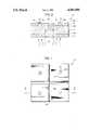
- FIG. 1is a top view, not to scale, of an array of radiation detectors constructed in accordance with the invention.
- FIG. 2is a cross-sectional view, not to scale, taken along the section line labeled 2-2 of FIG. 1.
- FIGS. 1 and 2show illustrative top and cross-sectional views, respectively, of a radiation detecting array 10.
- FIGS. 1 and 2are not drawn to scale.
- the array 10is comprised of Group II-VI material and a specific embodiment having a radiation absorbing layer comprised of HgCdTe will be described in detail below. It should be realized that the teaching of the invention is applicable to arrays comprised of other materials and to other families of materials such as Group III-V material.
- FIGS. 1 and 2illustrate a back-side illuminated two-dimensional array having four PV detectors the teaching of the invention is also applicable to single detectors and to one-dimensional and two-dimensional arrays comprised of more or less than four detectors.
- the teaching of the inventionis also applicable to front-side illuminated arrays.
- the array 10includes a substrate 12.
- the substrate 12is substantially transparent to incident IR radiation and is electrically insulating.
- the substrate 12is comprised of CdZnTe having a total thickness of approximately 900 microns.
- Overlying substrate 12is a radiation absorbing base layer 14 having a lower surface 14a in contact with the substrate 12 and an upper surface 14b.
- Base layer 14is comprised of p-type Hg 1-x Cd x Te wherein x has a value of approximately 0.6 to approximately 0.8 at the surface 14a and is graded in value such that at the surface 14b x has a value of approximately 0.2 for LWIR radiation, approximately 0.3 for MWIR radiation or approximately 0.4 for SWIR radiation.
- the energy band gap of the base layer 14nonlinearly decreases in width as the surface 14b is approached such that the desired final energy band gap value is asympototically approached through the upper several microns of base layer 14 material.
- Base layer 14has a thickness of approximately 15 microns.
- Hg 1-x Cd x Te cap layer 16Overlying the radiation absorbing base layer 14 is a graded composition Hg 1-x Cd x Te cap layer 16 that is compositionally graded to wider bandgap material comprised of CdTe, Hg 1-x Cd x Te, HgCdZnTe, Cd 1-y Zn y Te or combinations thereof at the upper surface 16a.
- the cap layer 16varies in composition from Hg 1-x Cd x Te, where x is less than approximately 0.4 at the surface 14b, to CdTe, where x has a value of approximately 1.0 at an upper surface 16a.
- the energy bandgap of the cap layer 16increases in width as a function of distance from the surface 14b and as the surface 16a is approached.
- Cap layer 16has a typical thickness of approximately one to approximately two microns. Lattice matching is not required, but a cap layer comprised of Cd 1-y Zn y Te can be lattice matched to HgCdTe by making y approximately 0.04. A lattice matched cap layer 16 provides advantages derived from reducing disorder at the CdZnTe/HgCdTe interface.
- the cap layer 16may be comprised of p-type material as shown in FIG. 2 or may be substantially undoped.
- the array 10includes ion implanted or diffused n-type regions 18 within the cap layer 16 for forming photodiode p-n junctions 18a. In electrical contact with the regions 18 is contact metalization 20 for coupling each of the junctions 18a to an external readout circuit (not shown). Boron is one suitable chemical species for implanting within the surface of the cap layer 16, and In is a suitable n-type diffusant.
- the implant or diffusion depthis controlled during processing such that the maximum depth of the region 18 is substantially equal to the thickness of the cap layer 16 such that the region 18 is substantially wholly contained within the wide bandgap material of the cap layer 16, and the p-n junction is located essentially at the surface 14b.
- a channel 22is etched partially into the compositionally graded p-type base layer 14 in order to substantially prevent crosstalk between the individual photodiodes.
- the channel 22operates to physically prevent photocarriers that are generated primarily in the longer wavelength HgCdTe material near a junction 18a from laterally diffusing to adjacent junctions.
- the channel 22is etched before the deposition of the cap layer 16 such that the exposed surfaces of the channel 22 are also passivated.
- the depth of the channel 22is typically from two to four microns and the width is typically equal to the depth or is somewhat wider.
- IR radiationis incident upon and passes through the transparent and electrically insulating substrate 12 and passes into and is absorbed within the electrically conducting p-type base layer 14.
- the absorbed radiationgenerates electron-hole pairs and the minority carrier electrons diffuse toward the p-n junctions 18a to create a current in an external circuit (not shown) connected between the n regions 18 and the base layer 14.
- junction 18ais located substantially within the wider bandgap cap layer 16, the same layer which also serves as an integral passivation.
- the depth of the ion implant or diffusionis controlled to place the electrical junction edge so as to minimize junction dark leakage current without significantly reducing quantum efficiency.
- This arrangementhas several advantages over conventional junctions implanted or diffused into a constant bandgap base layer. Specifically, leakage current is reduced and diode impedance is increased by forming one side of the junction in wider bandgap material. Also, since the bandgap of the cap layer is quite wide at the outer surface of the device (e.g. 1.6eV for CdTe), the cap layer forms a natural passivation which has been shown to reduce diode leakage current and improve stability during elevated temperature storage.
- the use of ion implantation or diffusion to form the junction 18aimproves junction uniformity. It also provides for reduced junction capacitance since the electrical junction is made smaller than the corresponding optical junction.
- the interdiffused cap layer 16may be created by a number of processes.
- One suitable processinvolves an annealed interdiffusion of CdTe with the base layer 14.
- Another suitable processinvolves an LPE, MBE, or MOCVD grown cap layer.
- Still another suitable processinvolves the diffusion of Cd and/or Zn into the base layer 14.
- the base layer 1may also be formed by LPE, MBE or MOCVD. It should be noted however that the compositional grading of the base and cap layers is best accomplished by the VPE and MOCVD growth techniques.
- a wet chemical etch through a suitably patterned maskis preferably employed to create the channels 22.
- the implanted or diffused junctionsare also formed through a suitably windowed mask. Subsequent metalization steps are performed such that the individual diodes can be coupled to suitable readout circuitry.
- RoAj at 195K for 4.5 micron cutoff devicesis 60 ohms-cm 2 with a 5 volt breakdown while conventional devices exhibit 10 ohms-cm 2 with a 1 volt breakdown.
- 1/f noise at 100 mV reverse bias and 1 Hzis 10 -5 V/ Hz as opposed to 10 -4 V/ Hz for conventional devices.
- RoAj at 120Kis approximately 2 ⁇ 106 ohms-cm 2 as compared with 2 ⁇ 104 ohms-cm 2 for conventional devices.
- bake stabilityis improved over conventional devices.
- the base layercould be n-type material and the regions within the cap layer could be p-type material.
Landscapes
- Light Receiving Elements (AREA)
- Solid State Image Pick-Up Elements (AREA)
Abstract
Description
Claims (20)
Priority Applications (5)
| Application Number | Priority Date | Filing Date | Title |
|---|---|---|---|
| US07/375,229US4961098A (en) | 1989-07-03 | 1989-07-03 | Heterojunction photodiode array |
| IL9463690AIL94636A (en) | 1989-07-03 | 1990-06-06 | Heterojunction photodiode array |
| DE69005048TDE69005048T2 (en) | 1989-07-03 | 1990-06-27 | Matrix of heterojunction photodiodes. |
| EP90112294AEP0406696B1 (en) | 1989-07-03 | 1990-06-27 | Heterojunction photodiode array |
| JP2174629AJPH0732263B2 (en) | 1989-07-03 | 1990-07-03 | Heterojunction photodiode array |
Applications Claiming Priority (1)
| Application Number | Priority Date | Filing Date | Title |
|---|---|---|---|
| US07/375,229US4961098A (en) | 1989-07-03 | 1989-07-03 | Heterojunction photodiode array |
Publications (1)
| Publication Number | Publication Date |
|---|---|
| US4961098Atrue US4961098A (en) | 1990-10-02 |
Family
ID=23480050
Family Applications (1)
| Application Number | Title | Priority Date | Filing Date |
|---|---|---|---|
| US07/375,229Expired - LifetimeUS4961098A (en) | 1989-07-03 | 1989-07-03 | Heterojunction photodiode array |
Country Status (5)
| Country | Link |
|---|---|
| US (1) | US4961098A (en) |
| EP (1) | EP0406696B1 (en) |
| JP (1) | JPH0732263B2 (en) |
| DE (1) | DE69005048T2 (en) |
| IL (1) | IL94636A (en) |
Cited By (15)
| Publication number | Priority date | Publication date | Assignee | Title |
|---|---|---|---|---|
| US5149956A (en)* | 1991-06-12 | 1992-09-22 | Santa Barbara Research Center | Two-color radiation detector array and methods of fabricating same |
| US5466953A (en)* | 1993-05-28 | 1995-11-14 | Santa Barbara Research Center | Denuded zone field effect photoconductive detector |
| WO1996010843A1 (en)* | 1994-09-30 | 1996-04-11 | The University Of Western Australia | Photosensitive semiconductor array |
| US6329679B1 (en)* | 1998-06-29 | 2001-12-11 | Hyundai Electronics Industries Co., Ltd. | Photodiode with increased photocollection area for image sensor |
| US20030071221A1 (en)* | 2001-10-12 | 2003-04-17 | Lockheed Martin Corporation | Planar geometry buried junction infrared detector and focal plane array |
| US6603184B2 (en) | 2000-09-06 | 2003-08-05 | Applied Optoelectronics, Inc. | Double heterostructure photodiode with graded minority-carrier blocking structures |
| US6753586B1 (en)* | 1998-03-09 | 2004-06-22 | Integration Associates Inc. | Distributed photodiode structure having majority dopant gradient and method for making same |
| US20040151443A1 (en)* | 2002-11-21 | 2004-08-05 | Toshio Mizue | Optical module |
| US20050056829A1 (en)* | 2003-09-17 | 2005-03-17 | Green Michael C. | Reducing dark current of photoconductor using heterojunction that maintains high x-ray sensitivity |
| US20070034898A1 (en)* | 2005-01-06 | 2007-02-15 | Rockwell Scientific Licensing, Llc | Heterojunction photodiode |
| US7459730B1 (en) | 2005-09-20 | 2008-12-02 | Drs Sensors & Targeting Systems, Inc. | Separate absorption and detection diode for VLWIR |
| FR3020176A1 (en)* | 2014-04-22 | 2015-10-23 | Commissariat Energie Atomique | MATRICE OF PHOTODIODS IN CDHGTE |
| EP2950347A1 (en)* | 2014-05-27 | 2015-12-02 | Commissariat à l'Énergie Atomique et aux Énergies Alternatives | Mesa photodiode array with improved mtf |
| EP2975643A1 (en)* | 2014-07-16 | 2016-01-20 | Commissariat à l'Énergie Atomique et aux Énergies Alternatives | Low-noise cdhgte photodiode array |
| CN114597271A (en)* | 2022-01-25 | 2022-06-07 | 国科大杭州高等研究院 | A novel photoelectric position-sensitive detector based on heterojunction two-dimensional electron gas and its preparation method |
Families Citing this family (2)
| Publication number | Priority date | Publication date | Assignee | Title |
|---|---|---|---|---|
| US5241196A (en)* | 1991-10-15 | 1993-08-31 | Santa Barbara Research Center | Photoresponsive device including composition grading and recessed contacts for trapping minority carriers |
| JPH08111539A (en)* | 1994-10-07 | 1996-04-30 | Nec Corp | Manufacture of photovoltaic type hgcdte infrared ray detector |
Citations (14)
| Publication number | Priority date | Publication date | Assignee | Title |
|---|---|---|---|---|
| US3677280A (en)* | 1971-06-21 | 1972-07-18 | Fairchild Camera Instr Co | Optimum high gain-bandwidth phototransistor structure |
| US3845494A (en)* | 1972-01-27 | 1974-10-29 | Telecommunications Sa | HgTe-CdTe PHOTOVOLTAIC DETECTORS |
| US3858306A (en)* | 1971-08-05 | 1975-01-07 | Honeywell Inc | Alloy junctions in mercury cadmium telluride |
| US3988774A (en)* | 1974-08-06 | 1976-10-26 | Societe Anonyme De Telecommunications | Process for producing a photodiode sensitive to infrared radiation |
| US4105478A (en)* | 1977-01-06 | 1978-08-08 | Honeywell, Inc. | Doping hgcdte with li |
| US4132999A (en)* | 1975-12-23 | 1979-01-02 | Societe Anonyme De Telecommunications | Semiconductor devices |
| US4206003A (en)* | 1977-07-05 | 1980-06-03 | Honeywell Inc. | Method of forming a mercury cadmium telluride photodiode |
| GB2100927A (en)* | 1981-06-24 | 1983-01-06 | Secr Defence | Photo diodes |
| US4411732A (en)* | 1981-03-27 | 1983-10-25 | U.S. Philips Corporation | Method of manufacturing a detector device |
| US4532699A (en)* | 1982-11-30 | 1985-08-06 | Societe Anonyme De Telecommunications | Process for manufacturing a matrix infrared detector with illumination by the front face |
| JPS60157273A (en)* | 1984-01-25 | 1985-08-17 | Matsushita Electric Ind Co Ltd | Manufacture of thin film photo transistor |
| US4639756A (en)* | 1986-05-05 | 1987-01-27 | Santa Barbara Research Center | Graded gap inversion layer photodiode array |
| US4646120A (en)* | 1985-03-21 | 1987-02-24 | The United States Of America As Represented By The Secretary Of The Army | Photodiode array |
| US4766084A (en)* | 1986-09-19 | 1988-08-23 | Commissariat A L'energie Atomique | Process for the production of an electric contact on a HgCdTe substrate with a P conductivity and application to the production of an N/P diode |
- 1989
- 1989-07-03USUS07/375,229patent/US4961098A/ennot_activeExpired - Lifetime
- 1990
- 1990-06-06ILIL9463690Apatent/IL94636A/ennot_activeIP Right Cessation
- 1990-06-27EPEP90112294Apatent/EP0406696B1/ennot_activeExpired - Lifetime
- 1990-06-27DEDE69005048Tpatent/DE69005048T2/ennot_activeExpired - Fee Related
- 1990-07-03JPJP2174629Apatent/JPH0732263B2/ennot_activeExpired - Lifetime
Patent Citations (14)
| Publication number | Priority date | Publication date | Assignee | Title |
|---|---|---|---|---|
| US3677280A (en)* | 1971-06-21 | 1972-07-18 | Fairchild Camera Instr Co | Optimum high gain-bandwidth phototransistor structure |
| US3858306A (en)* | 1971-08-05 | 1975-01-07 | Honeywell Inc | Alloy junctions in mercury cadmium telluride |
| US3845494A (en)* | 1972-01-27 | 1974-10-29 | Telecommunications Sa | HgTe-CdTe PHOTOVOLTAIC DETECTORS |
| US3988774A (en)* | 1974-08-06 | 1976-10-26 | Societe Anonyme De Telecommunications | Process for producing a photodiode sensitive to infrared radiation |
| US4132999A (en)* | 1975-12-23 | 1979-01-02 | Societe Anonyme De Telecommunications | Semiconductor devices |
| US4105478A (en)* | 1977-01-06 | 1978-08-08 | Honeywell, Inc. | Doping hgcdte with li |
| US4206003A (en)* | 1977-07-05 | 1980-06-03 | Honeywell Inc. | Method of forming a mercury cadmium telluride photodiode |
| US4411732A (en)* | 1981-03-27 | 1983-10-25 | U.S. Philips Corporation | Method of manufacturing a detector device |
| GB2100927A (en)* | 1981-06-24 | 1983-01-06 | Secr Defence | Photo diodes |
| US4532699A (en)* | 1982-11-30 | 1985-08-06 | Societe Anonyme De Telecommunications | Process for manufacturing a matrix infrared detector with illumination by the front face |
| JPS60157273A (en)* | 1984-01-25 | 1985-08-17 | Matsushita Electric Ind Co Ltd | Manufacture of thin film photo transistor |
| US4646120A (en)* | 1985-03-21 | 1987-02-24 | The United States Of America As Represented By The Secretary Of The Army | Photodiode array |
| US4639756A (en)* | 1986-05-05 | 1987-01-27 | Santa Barbara Research Center | Graded gap inversion layer photodiode array |
| US4766084A (en)* | 1986-09-19 | 1988-08-23 | Commissariat A L'energie Atomique | Process for the production of an electric contact on a HgCdTe substrate with a P conductivity and application to the production of an N/P diode |
Non-Patent Citations (6)
| Title |
|---|
| Almasi et al., "CdTe--HgTe Heterostructures", Journal of Applied Physics, vol. 39, No. 1, Jan. 1968, pp. 233-245. |
| Almasi et al., CdTe HgTe Heterostructures , Journal of Applied Physics, vol. 39, No. 1, Jan. 1968, pp. 233 245.* |
| Lanir et al., "Backside-Illuminated HgCdTe/CdTe Photodiodes," Appl. Phys. Lett. 34(1), Jan. 1, 1979, pp. 50-52. |
| Lanir et al., Backside Illuminated HgCdTe/CdTe Photodiodes, Appl. Phys. Lett. 34(1), Jan. 1, 1979, pp. 50 52.* |
| Stelzer et al., "Mercury Cadmium Telluride as an Infrared Detector Material," IEEE Transactions on Electron Devices, vol. ED-16, No. 10, Oct. 1969, pp. 880-884. |
| Stelzer et al., Mercury Cadmium Telluride as an Infrared Detector Material, IEEE Transactions on Electron Devices, vol. ED 16, No. 10, Oct. 1969, pp. 880 884.* |
Cited By (28)
| Publication number | Priority date | Publication date | Assignee | Title |
|---|---|---|---|---|
| US5149956A (en)* | 1991-06-12 | 1992-09-22 | Santa Barbara Research Center | Two-color radiation detector array and methods of fabricating same |
| US5466953A (en)* | 1993-05-28 | 1995-11-14 | Santa Barbara Research Center | Denuded zone field effect photoconductive detector |
| WO1996010843A1 (en)* | 1994-09-30 | 1996-04-11 | The University Of Western Australia | Photosensitive semiconductor array |
| US6753586B1 (en)* | 1998-03-09 | 2004-06-22 | Integration Associates Inc. | Distributed photodiode structure having majority dopant gradient and method for making same |
| US6723580B2 (en) | 1998-06-29 | 2004-04-20 | Hyundai Electronics Industries Co., Ltd. | Method of forming a photodiode for an image sensor |
| US6329679B1 (en)* | 1998-06-29 | 2001-12-11 | Hyundai Electronics Industries Co., Ltd. | Photodiode with increased photocollection area for image sensor |
| US6787386B2 (en) | 1998-06-29 | 2004-09-07 | Hynix Semiconductor, Inc. | Method of forming a photodiode for an image sensor |
| US6603184B2 (en) | 2000-09-06 | 2003-08-05 | Applied Optoelectronics, Inc. | Double heterostructure photodiode with graded minority-carrier blocking structures |
| US20030071221A1 (en)* | 2001-10-12 | 2003-04-17 | Lockheed Martin Corporation | Planar geometry buried junction infrared detector and focal plane array |
| US7041983B2 (en)* | 2001-10-12 | 2006-05-09 | Lockheed Martin Corporation | Planar geometry buried junction infrared detector and focal plane array |
| US20040151443A1 (en)* | 2002-11-21 | 2004-08-05 | Toshio Mizue | Optical module |
| US7121743B2 (en)* | 2002-11-21 | 2006-10-17 | Sumitomo Electric Industries, Ltd. | Optical module |
| US20050056829A1 (en)* | 2003-09-17 | 2005-03-17 | Green Michael C. | Reducing dark current of photoconductor using heterojunction that maintains high x-ray sensitivity |
| US7368762B2 (en) | 2005-01-06 | 2008-05-06 | Teledyne Licensing, Llc | Heterojunction photodiode |
| US20070034898A1 (en)* | 2005-01-06 | 2007-02-15 | Rockwell Scientific Licensing, Llc | Heterojunction photodiode |
| US7459730B1 (en) | 2005-09-20 | 2008-12-02 | Drs Sensors & Targeting Systems, Inc. | Separate absorption and detection diode for VLWIR |
| US7504672B1 (en) | 2005-09-20 | 2009-03-17 | Drs Sensors & Targeting Systems, Inc. | Separate absorption and detection diode |
| US7608830B1 (en) | 2005-09-20 | 2009-10-27 | Drs Sensors & Targeting Systems, Inc. | Separate absorption and detection diode for two-color operation |
| US9397244B2 (en) | 2014-04-22 | 2016-07-19 | Commissariat A' L'energie Atomique Et Aux Energies Alternatives | CdHgTe photodiodes array |
| FR3020176A1 (en)* | 2014-04-22 | 2015-10-23 | Commissariat Energie Atomique | MATRICE OF PHOTODIODS IN CDHGTE |
| EP2937902A1 (en)* | 2014-04-22 | 2015-10-28 | Commissariat à l'Énergie Atomique et aux Énergies Alternatives | Cdhgte photodiode array |
| EP2950347A1 (en)* | 2014-05-27 | 2015-12-02 | Commissariat à l'Énergie Atomique et aux Énergies Alternatives | Mesa photodiode array with improved mtf |
| FR3021807A1 (en)* | 2014-05-27 | 2015-12-04 | Commissariat Energie Atomique | IMPROVED FTM MESA PHOTODIOD MATRIX MATRIX |
| US10177193B2 (en) | 2014-05-27 | 2019-01-08 | Commissariat à l'énergie atomique et aux énergies alternatives | Array of mesa photodiodes with an improved MTF |
| EP2975643A1 (en)* | 2014-07-16 | 2016-01-20 | Commissariat à l'Énergie Atomique et aux Énergies Alternatives | Low-noise cdhgte photodiode array |
| FR3023976A1 (en)* | 2014-07-16 | 2016-01-22 | Commissariat Energie Atomique | LOW NOISE CDHGTE PHOTODIOD MATRIX |
| US9450013B2 (en) | 2014-07-16 | 2016-09-20 | Commissariat A L'energie Atomique Et Aux Energies Alternatives | Low noise CdHgTe photodiode array |
| CN114597271A (en)* | 2022-01-25 | 2022-06-07 | 国科大杭州高等研究院 | A novel photoelectric position-sensitive detector based on heterojunction two-dimensional electron gas and its preparation method |
Also Published As
| Publication number | Publication date |
|---|---|
| IL94636A0 (en) | 1991-04-15 |
| EP0406696B1 (en) | 1993-12-08 |
| EP0406696A2 (en) | 1991-01-09 |
| DE69005048T2 (en) | 1994-07-07 |
| IL94636A (en) | 1994-10-07 |
| JPH0732263B2 (en) | 1995-04-10 |
| DE69005048D1 (en) | 1994-01-20 |
| EP0406696A3 (en) | 1991-04-03 |
| JPH0346279A (en) | 1991-02-27 |
Similar Documents
| Publication | Publication Date | Title |
|---|---|---|
| US5049962A (en) | Control of optical crosstalk between adjacent photodetecting regions | |
| US4961098A (en) | Heterojunction photodiode array | |
| US5149956A (en) | Two-color radiation detector array and methods of fabricating same | |
| US5559336A (en) | Integrated LPE-grown structure for simultaneous detection of infrared radiation in two bands | |
| US5113076A (en) | Two terminal multi-band infrared radiation detector | |
| US11257973B2 (en) | Method for passing photovoltaic current between a subcell formed from a group II-VI semiconductor material and a subcell formed from a group IV semiconductor material | |
| US4665277A (en) | Floating emitter solar cell | |
| US8766393B2 (en) | Low-noise semiconductor photodetectors | |
| US5430321A (en) | Photodiode structure | |
| EP0473197B1 (en) | Photo-sensing device | |
| JP3124731B2 (en) | Dual color detector for p + / n long-wave infrared and p + / n mid-wave infrared | |
| US5457331A (en) | Dual-band infrared radiation detector optimized for fabrication in compositionally graded HgCdTe | |
| US20050156192A1 (en) | Planar avalanche photodiode | |
| US8697554B2 (en) | Lateral collection architecture for SLS detectors | |
| US5936268A (en) | Epitaxial passivation of group II-VI infrared photodetectors | |
| US9455364B2 (en) | Tunnel homojunctions in group IV / group II-VI multijunction solar cells | |
| US5599733A (en) | Method using cadmium-rich CdTe for lowering the metal vacancy concentrations of HgCdTe surfaces | |
| US4544938A (en) | Wavelength-selective photodetector | |
| US5059786A (en) | Multi-color coincident infrared detector | |
| EP1470574B1 (en) | High speed pin photodiode with increased responsivity | |
| Rutkowski | Planar junction formation in HgCdTe infrared detectors | |
| US4282541A (en) | Planar P-I-N photodetectors | |
| US5466953A (en) | Denuded zone field effect photoconductive detector | |
| US5177580A (en) | Implant guarded mesa having improved detector uniformity | |
| US20250098342A1 (en) | Convex photodiode imaging array |
Legal Events
| Date | Code | Title | Description |
|---|---|---|---|
| AS | Assignment | Owner name:SANTA BARBARA RESEARCH CENTER, GOLETA, CA, A CORP. Free format text:ASSIGNMENT OF ASSIGNORS INTEREST.;ASSIGNORS:ROSBECK, JOSEPH P.;COCKRUM, CHARLES A.;REEL/FRAME:005103/0168 Effective date:19890628 | |
| STCF | Information on status: patent grant | Free format text:PATENTED CASE | |
| FEPP | Fee payment procedure | Free format text:PAYOR NUMBER ASSIGNED (ORIGINAL EVENT CODE: ASPN); ENTITY STATUS OF PATENT OWNER: LARGE ENTITY | |
| FPAY | Fee payment | Year of fee payment:4 | |
| FPAY | Fee payment | Year of fee payment:8 | |
| FPAY | Fee payment | Year of fee payment:12 | |
| AS | Assignment | Owner name:HE HOLDINGS, INC., CALIFORNIA Free format text:MERGER;ASSIGNOR:HUGHES AIRCRAFT COMPANY;REEL/FRAME:016722/0088 Effective date:19971216 Owner name:HUGHES AIRCRAFT COMPANY, VIRGINIA Free format text:MERGER;ASSIGNOR:SANTA BARBARA RESEARCH CENTER;REEL/FRAME:016712/0877 Effective date:19961205 Owner name:RAYTHEON COMPANY, MASSACHUSETTS Free format text:MERGER;ASSIGNOR:HE HOLDINGS, INC.;REEL/FRAME:016722/0093 Effective date:19971217 |