US4959700A - Insulated gate field effect transistor and its manufacturing method - Google Patents
Insulated gate field effect transistor and its manufacturing methodDownload PDFInfo
- Publication number
- US4959700A US4959700AUS07/153,477US15347788AUS4959700AUS 4959700 AUS4959700 AUS 4959700AUS 15347788 AUS15347788 AUS 15347788AUS 4959700 AUS4959700 AUS 4959700A
- Authority
- US
- United States
- Prior art keywords
- semiconductor layer
- source
- region
- regions
- substrate
- Prior art date
- Legal status (The legal status is an assumption and is not a legal conclusion. Google has not performed a legal analysis and makes no representation as to the accuracy of the status listed.)
- Expired - Lifetime
Links
- 230000005669field effectEffects0.000titleclaimsdescription11
- 238000004519manufacturing processMethods0.000titledescription12
- 239000004065semiconductorSubstances0.000claimsabstractdescription125
- 239000000758substrateSubstances0.000claimsabstractdescription36
- 230000001678irradiating effectEffects0.000claimsabstract4
- 238000002425crystallisationMethods0.000claimsdescription8
- 230000008025crystallizationEffects0.000claimsdescription7
- 230000000694effectsEffects0.000abstract1
- 239000013078crystalSubstances0.000description56
- 108091006146ChannelsProteins0.000description40
- 230000006798recombinationEffects0.000description27
- 230000003287optical effectEffects0.000description8
- 239000012535impuritySubstances0.000description7
- 229910052698phosphorusInorganic materials0.000description6
- 238000010438heat treatmentMethods0.000description5
- 238000000137annealingMethods0.000description4
- 238000000034methodMethods0.000description4
- 229910052757nitrogenInorganic materials0.000description4
- 239000000203mixtureSubstances0.000description3
- 239000011574phosphorusSubstances0.000description3
- IJGRMHOSHXDMSA-UHFFFAOYSA-NAtomic nitrogenChemical compoundN#NIJGRMHOSHXDMSA-UHFFFAOYSA-N0.000description2
- OAICVXFJPJFONN-UHFFFAOYSA-NPhosphorusChemical compound[P]OAICVXFJPJFONN-UHFFFAOYSA-N0.000description2
- 229910052785arsenicInorganic materials0.000description2
- RQNWIZPPADIBDY-UHFFFAOYSA-Narsenic atomChemical compound[As]RQNWIZPPADIBDY-UHFFFAOYSA-N0.000description2
- QVGXLLKOCUKJST-UHFFFAOYSA-Natomic oxygenChemical compound[O]QVGXLLKOCUKJST-UHFFFAOYSA-N0.000description2
- 230000015572biosynthetic processEffects0.000description2
- 239000000969carrierSubstances0.000description2
- 238000010276constructionMethods0.000description2
- 230000007547defectEffects0.000description2
- 238000009792diffusion processMethods0.000description2
- 229910021424microcrystalline siliconInorganic materials0.000description2
- 230000004048modificationEffects0.000description2
- 238000012986modificationMethods0.000description2
- 229910021421monocrystalline siliconInorganic materials0.000description2
- 229910052760oxygenInorganic materials0.000description2
- 239000001301oxygenSubstances0.000description2
- 229910021420polycrystalline siliconInorganic materials0.000description2
- 238000005036potential barrierMethods0.000description2
- 230000008569processEffects0.000description2
- OKTJSMMVPCPJKN-UHFFFAOYSA-NCarbonChemical compound[C]OKTJSMMVPCPJKN-UHFFFAOYSA-N0.000description1
- PXGOKWXKJXAPGV-UHFFFAOYSA-NFluorineChemical compoundFFPXGOKWXKJXAPGV-UHFFFAOYSA-N0.000description1
- UFHFLCQGNIYNRP-UHFFFAOYSA-NHydrogenChemical compound[H][H]UFHFLCQGNIYNRP-UHFFFAOYSA-N0.000description1
- 102000004129N-Type Calcium ChannelsHuman genes0.000description1
- 108090000699N-Type Calcium ChannelsProteins0.000description1
- 229910052581Si3N4Inorganic materials0.000description1
- VYPSYNLAJGMNEJ-UHFFFAOYSA-NSilicium dioxideChemical compoundO=[Si]=OVYPSYNLAJGMNEJ-UHFFFAOYSA-N0.000description1
- 230000004913activationEffects0.000description1
- 229910021417amorphous siliconInorganic materials0.000description1
- 229910052799carbonInorganic materials0.000description1
- 230000015556catabolic processEffects0.000description1
- 239000000919ceramicSubstances0.000description1
- 238000005530etchingMethods0.000description1
- 238000002474experimental methodMethods0.000description1
- -1fluorineChemical class0.000description1
- 229910052731fluorineInorganic materials0.000description1
- 239000011737fluorineSubstances0.000description1
- 239000007789gasSubstances0.000description1
- 239000011521glassSubstances0.000description1
- 229910052736halogenInorganic materials0.000description1
- 150000002367halogensChemical class0.000description1
- 229910052739hydrogenInorganic materials0.000description1
- 239000001257hydrogenSubstances0.000description1
- 238000002513implantationMethods0.000description1
- 239000011810insulating materialSubstances0.000description1
- 238000009413insulationMethods0.000description1
- 238000005468ion implantationMethods0.000description1
- QSHDDOUJBYECFT-UHFFFAOYSA-NmercuryChemical compound[Hg]QSHDDOUJBYECFT-UHFFFAOYSA-N0.000description1
- 229910052753mercuryInorganic materials0.000description1
- 229920002120photoresistant polymerPolymers0.000description1
- 238000005268plasma chemical vapour depositionMethods0.000description1
- 238000002360preparation methodMethods0.000description1
- HQVNEWCFYHHQES-UHFFFAOYSA-Nsilicon nitrideChemical compoundN12[Si]34N5[Si]62N3[Si]51N64HQVNEWCFYHHQES-UHFFFAOYSA-N0.000description1
- 229920003002synthetic resinPolymers0.000description1
- 239000000057synthetic resinSubstances0.000description1
Images


Classifications
- H—ELECTRICITY
- H10—SEMICONDUCTOR DEVICES; ELECTRIC SOLID-STATE DEVICES NOT OTHERWISE PROVIDED FOR
- H10D—INORGANIC ELECTRIC SEMICONDUCTOR DEVICES
- H10D30/00—Field-effect transistors [FET]
- H10D30/01—Manufacture or treatment
- H10D30/021—Manufacture or treatment of FETs having insulated gates [IGFET]
- H10D30/031—Manufacture or treatment of FETs having insulated gates [IGFET] of thin-film transistors [TFT]
- H10D30/0312—Manufacture or treatment of FETs having insulated gates [IGFET] of thin-film transistors [TFT] characterised by the gate electrodes
- H10D30/0314—Manufacture or treatment of FETs having insulated gates [IGFET] of thin-film transistors [TFT] characterised by the gate electrodes of lateral top-gate TFTs comprising only a single gate
- H—ELECTRICITY
- H01—ELECTRIC ELEMENTS
- H01L—SEMICONDUCTOR DEVICES NOT COVERED BY CLASS H10
- H01L21/00—Processes or apparatus adapted for the manufacture or treatment of semiconductor or solid state devices or of parts thereof
- H01L21/02—Manufacture or treatment of semiconductor devices or of parts thereof
- H01L21/02104—Forming layers
- H01L21/02365—Forming inorganic semiconducting materials on a substrate
- H01L21/02367—Substrates
- H01L21/0237—Materials
- H01L21/0242—Crystalline insulating materials
- H—ELECTRICITY
- H01—ELECTRIC ELEMENTS
- H01L—SEMICONDUCTOR DEVICES NOT COVERED BY CLASS H10
- H01L21/00—Processes or apparatus adapted for the manufacture or treatment of semiconductor or solid state devices or of parts thereof
- H01L21/02—Manufacture or treatment of semiconductor devices or of parts thereof
- H01L21/02104—Forming layers
- H01L21/02365—Forming inorganic semiconducting materials on a substrate
- H01L21/02436—Intermediate layers between substrates and deposited layers
- H01L21/02439—Materials
- H01L21/02441—Group 14 semiconducting materials
- H01L21/0245—Silicon, silicon germanium, germanium
- H—ELECTRICITY
- H01—ELECTRIC ELEMENTS
- H01L—SEMICONDUCTOR DEVICES NOT COVERED BY CLASS H10
- H01L21/00—Processes or apparatus adapted for the manufacture or treatment of semiconductor or solid state devices or of parts thereof
- H01L21/02—Manufacture or treatment of semiconductor devices or of parts thereof
- H01L21/02104—Forming layers
- H01L21/02365—Forming inorganic semiconducting materials on a substrate
- H01L21/02436—Intermediate layers between substrates and deposited layers
- H01L21/02439—Materials
- H01L21/02488—Insulating materials
- H—ELECTRICITY
- H01—ELECTRIC ELEMENTS
- H01L—SEMICONDUCTOR DEVICES NOT COVERED BY CLASS H10
- H01L21/00—Processes or apparatus adapted for the manufacture or treatment of semiconductor or solid state devices or of parts thereof
- H01L21/02—Manufacture or treatment of semiconductor devices or of parts thereof
- H01L21/02104—Forming layers
- H01L21/02365—Forming inorganic semiconducting materials on a substrate
- H01L21/02518—Deposited layers
- H01L21/02521—Materials
- H01L21/02524—Group 14 semiconducting materials
- H01L21/02532—Silicon, silicon germanium, germanium
- H—ELECTRICITY
- H01—ELECTRIC ELEMENTS
- H01L—SEMICONDUCTOR DEVICES NOT COVERED BY CLASS H10
- H01L21/00—Processes or apparatus adapted for the manufacture or treatment of semiconductor or solid state devices or of parts thereof
- H01L21/02—Manufacture or treatment of semiconductor devices or of parts thereof
- H01L21/02104—Forming layers
- H01L21/02365—Forming inorganic semiconducting materials on a substrate
- H01L21/02518—Deposited layers
- H01L21/0257—Doping during depositing
- H01L21/02573—Conductivity type
- H01L21/02576—N-type
- H—ELECTRICITY
- H01—ELECTRIC ELEMENTS
- H01L—SEMICONDUCTOR DEVICES NOT COVERED BY CLASS H10
- H01L21/00—Processes or apparatus adapted for the manufacture or treatment of semiconductor or solid state devices or of parts thereof
- H01L21/02—Manufacture or treatment of semiconductor devices or of parts thereof
- H01L21/02104—Forming layers
- H01L21/02365—Forming inorganic semiconducting materials on a substrate
- H01L21/02656—Special treatments
- H01L21/02664—Aftertreatments
- H01L21/02667—Crystallisation or recrystallisation of non-monocrystalline semiconductor materials, e.g. regrowth
- H—ELECTRICITY
- H01—ELECTRIC ELEMENTS
- H01L—SEMICONDUCTOR DEVICES NOT COVERED BY CLASS H10
- H01L21/00—Processes or apparatus adapted for the manufacture or treatment of semiconductor or solid state devices or of parts thereof
- H01L21/02—Manufacture or treatment of semiconductor devices or of parts thereof
- H01L21/04—Manufacture or treatment of semiconductor devices or of parts thereof the devices having potential barriers, e.g. a PN junction, depletion layer or carrier concentration layer
- H01L21/18—Manufacture or treatment of semiconductor devices or of parts thereof the devices having potential barriers, e.g. a PN junction, depletion layer or carrier concentration layer the devices having semiconductor bodies comprising elements of Group IV of the Periodic Table or AIIIBV compounds with or without impurities, e.g. doping materials
- H01L21/26—Bombardment with radiation
- H01L21/263—Bombardment with radiation with high-energy radiation
- H01L21/268—Bombardment with radiation with high-energy radiation using electromagnetic radiation, e.g. laser radiation
- H—ELECTRICITY
- H10—SEMICONDUCTOR DEVICES; ELECTRIC SOLID-STATE DEVICES NOT OTHERWISE PROVIDED FOR
- H10D—INORGANIC ELECTRIC SEMICONDUCTOR DEVICES
- H10D30/00—Field-effect transistors [FET]
- H10D30/01—Manufacture or treatment
- H10D30/021—Manufacture or treatment of FETs having insulated gates [IGFET]
- H10D30/031—Manufacture or treatment of FETs having insulated gates [IGFET] of thin-film transistors [TFT]
- H10D30/0321—Manufacture or treatment of FETs having insulated gates [IGFET] of thin-film transistors [TFT] comprising silicon, e.g. amorphous silicon or polysilicon
- H—ELECTRICITY
- H10—SEMICONDUCTOR DEVICES; ELECTRIC SOLID-STATE DEVICES NOT OTHERWISE PROVIDED FOR
- H10D—INORGANIC ELECTRIC SEMICONDUCTOR DEVICES
- H10D30/00—Field-effect transistors [FET]
- H10D30/60—Insulated-gate field-effect transistors [IGFET]
- H10D30/67—Thin-film transistors [TFT]
- H10D30/6704—Thin-film transistors [TFT] having supplementary regions or layers in the thin films or in the insulated bulk substrates for controlling properties of the device
- H10D30/6713—Thin-film transistors [TFT] having supplementary regions or layers in the thin films or in the insulated bulk substrates for controlling properties of the device characterised by the properties of the source or drain regions, e.g. compositions or sectional shapes
- H—ELECTRICITY
- H10—SEMICONDUCTOR DEVICES; ELECTRIC SOLID-STATE DEVICES NOT OTHERWISE PROVIDED FOR
- H10D—INORGANIC ELECTRIC SEMICONDUCTOR DEVICES
- H10D30/00—Field-effect transistors [FET]
- H10D30/60—Insulated-gate field-effect transistors [IGFET]
- H10D30/67—Thin-film transistors [TFT]
- H10D30/6729—Thin-film transistors [TFT] characterised by the electrodes
- H10D30/673—Thin-film transistors [TFT] characterised by the electrodes characterised by the shapes, relative sizes or dispositions of the gate electrodes
- H10D30/6731—Top-gate only TFTs
- H—ELECTRICITY
- H10—SEMICONDUCTOR DEVICES; ELECTRIC SOLID-STATE DEVICES NOT OTHERWISE PROVIDED FOR
- H10D—INORGANIC ELECTRIC SEMICONDUCTOR DEVICES
- H10D30/00—Field-effect transistors [FET]
- H10D30/60—Insulated-gate field-effect transistors [IGFET]
- H10D30/67—Thin-film transistors [TFT]
- H10D30/674—Thin-film transistors [TFT] characterised by the active materials
- H10D30/6741—Group IV materials, e.g. germanium or silicon carbide
- H10D30/6743—Silicon
- H10D30/6746—Amorphous silicon
- Y—GENERAL TAGGING OF NEW TECHNOLOGICAL DEVELOPMENTS; GENERAL TAGGING OF CROSS-SECTIONAL TECHNOLOGIES SPANNING OVER SEVERAL SECTIONS OF THE IPC; TECHNICAL SUBJECTS COVERED BY FORMER USPC CROSS-REFERENCE ART COLLECTIONS [XRACs] AND DIGESTS
- Y10—TECHNICAL SUBJECTS COVERED BY FORMER USPC
- Y10S—TECHNICAL SUBJECTS COVERED BY FORMER USPC CROSS-REFERENCE ART COLLECTIONS [XRACs] AND DIGESTS
- Y10S257/00—Active solid-state devices, e.g. transistors, solid-state diodes
- Y10S257/914—Polysilicon containing oxygen, nitrogen, or carbon, e.g. sipos
Definitions
- the present inventionrelates to an insulated gate field effect transistor (herein after refer to as an insulated gate FET or an FET) and its manufacturing method.
- an insulated gate field effect transistorherein after refer to as an insulated gate FET or an FET
- an insulated gate FET of the typethat it has a high resistivity semiconductor layer formed on a substrate having an insulating surface, a gate electrode formed on the semiconductor layer with a gate insulating layer sandwiched therebetween in a manner to divide the semiconductor into two as viewed from above, and N or P conductivity type source and drain regions formed in the semiconductor layer in a manner to leave a channel forming region between first and second regions on both sides of the gate electrode as viewed from above, the source and drain regions being lower in resistivity than the channel region.
- the insulated gate FET of such a constructionis called an N-channel type or P-channel type insulated gate FET depending upon whether the source and drain regions are the N or P conductivity type, and it operates in such a manner as follows:
- the insulated gate FETWhen supplied with a control voltage across the source region and the gate electrode with a DC power source connected across the source and drain regions via a load, the insulated gate FET remains in the OFF state if the control voltage is lower than a certain threshold voltage when the FET is the N-channel type, or if the control voltage is higher than the threshold voltage when the FET is the P-channel type. In this case, substantially no current flow (drain current) is caused in the drain region, supplying no current to the load.
- a channel region of the same conductivity type as that of the source and drain regionsis formed in the channel forming region to extend between the source and drain regions on the side of the gate insulating layer, and the FET is turned ON to cause the drain current to flow, feeling current to the load
- the entire region of the semiconductor layeris formed of a single-crystal semiconductor, and accordingly, the channel forming region, the first and second regions and the source and drain regions formed therein, respectively, are all formed of the single-crystal semiconductor.
- the semiconductor layercannot be formed on the substrate unless the substrate is made of an insulating or semi-insulating single-crystal semiconductor.
- the semiconductor layerwhen the semiconductor layer is formed of the single-crystal semiconductor layer, especially when the channel forming region is formed of the single-crystal semiconductor, it has a smaller optical energy gap than does it when formed of a non-single-crystal semiconductor.
- the optical energy gap of the channel forming regionis 1.1 eV.
- the drain currentis small but larger than in the case where the channel forming region is formed of the non-single-crystal semiconductor.
- the abovesaid insulated gate FETis poorer in the OFF characteristic than in the case where the channel forming region is made of the non-single-crystal semiconductor.
- Another modified form of the above insulated gate FET heretofore proposedhas such a structure that the entire region of the semiconductor layer is formed of a non-single-crystal semiconductor doped with a recombination center neutralizer.
- the semiconductor layercan be formed on the substrate.
- the channel forming regionis made of the non-single-crystal semiconductor doped with a recombination center neutralizer, it has a larger optical energy gap than in the case where it is formed of the single-crystal semiconductor, so long as it is sufficiently doped with the recombination center neutralizer.
- the channel forming regionhas an optical energy gap in the range of 1.7 to 1.8 eV.
- the drain currentwill be markedly small, negligible as compared with that when the channel forming region is formed of the single-crystal semiconductor. Accordingly, so long as the semiconductor layer is sufficiently doped with the recombination center neutralizer, the FET will exhibit a more excellent OFF characteristic than does it when the channel forming region is made of the single-crystal semiconductor.
- impurity-doped regionsare formed in the first and second regions, for example, by ion implantation of an N- or P-type impurity, and then the source and drain regions are formed by heat treatment for the activation of the impurity doped in the impurity-doped regions.
- the recombination center neutralizer doped in the channel forming regionis diffused therefrom to the outside by the heat. Therefore, the channel forming region contains no required and sufficient amount of recombination center neutralizer, and hence has a smaller optical energy gap than the predetermined.
- the conventional insulated gate FET with the semiconductor layer formed of the non-single-crystal semiconductorpossesses an excellent OFF characteristic as compared with the case where the channel forming region is made of the single-crystal semiconductor, but the OFF characteristic is not fully satisfactory.
- the source and drain regionsare also obtained by heat treatment, the recombination center neutralizer doped therein is diffused to the outside during the heat treatment.
- the source and drain regionshave the same optical energy gap as that of the channel forming region, there is set up between each of the source and drain regions and the channel forming region substantially no or very small potential barrier against carriers flowing from the source or drain regions toward the channel forming region.
- the semiconductor layer, and accordingly the source and drain regionsare formed of the non-single-crystal semiconductor, they has the same degree of crystallization as that of the channel forming region and a far higher resistance than in the case where they are made of the single-crystal semiconductor.
- the speed of switching between the ON and the OFF stateis lower than in the case where the source and drain regions are formed of the single-crystal semiconductor. Accordingly, this FET has the defect that its ON-OFF operation cannot be achieved at high speed.
- Another object of the present inventionis to provide a novel method for the manufacture of such a novel insulated gate FET.
- the insulated gate FET of the present inventionhas also the same structure as the above-described conventional insulated gate FET. That is, it has a high resistivity semiconductor layer formed on a substrate having an insulating surface, a gate electrode formed on the semiconductor layer with a gate insulating layer sandwiched therebetween so that it separates the semiconductor layer into two as viewed from above, and N or P conductivity type source and drain regions formed in the semiconductor layer so that they define a channel forming region between first and second regions on both sides of the gate electrode as viewed from above and extend vertically from the upper surface of the first and second regions toward the substrate, the source and drain regions having a lower resistivity than that of the channel forming region.
- the semiconductor layeris formed of a non-single-crystal semiconductor doped with a required and sufficient amount of recombination center neutralizer, and accordingly, the channel forming region is also formed of such a non-single-crystal semiconductor.
- the first and second regions which constitute the source and drain regions in the semiconductor layerthere are provided on the sides of the source and drain regions, respectively, crystallized regions which have a higher degree of crystallization than the channel forming region and are doped with the recombination center neutralizer.
- the insulated gate FET of the present inventionis identical in construction with the aforesaid conventional insulated gage FET which has the semiconductor layer formed of the non-single-crystal semiconductor, except the inclusion of the abovesaid crystallized regions in the semiconductor layer.
- the insulated gate FET of the present inventionalso operates in the same manner as the aforementioned conventional FET. That is, when supplied with a control voltage across the source region and the gate electrode with the power source connected across the source and drain regions via a load, it remains in the OFF state and causes no current flow to the load if the control voltage is lower (or higher) than a certain threshold voltage, and if the control voltage is higher (or lower) than the threshold voltage, it is turned ON to cause drain current to flow, supplying current to the load.
- the insulated gate FET of the present inventionhas also the semiconductor layer forced of the non-single-crystal semiconductor, and hence it is free from the requirement that the substrate be an insulating or semi-insulating single-crystal semiconductor, as is the case with the conventional FET of this kind.
- the insulated gate FET of the present inventionexhibits an excellent OFF characteristic over the FET in which the channel forming region is made of the single-crystal semiconductor.
- the channel forming regionis doped with a required and sufficient amount of recombination center neutralizer, as will be evident from the manufacturing method of the present invention described later. Accordingly, the channel forming region has a predetermined optical energy gap, ensuring to provide an excellent OFF characteristic as compared with that of the conventional FET which has the semiconductor layer formed of the non-single-crystal semiconductor.
- the crystallized regionswhich have a higher degree of crystallization than the channel forming region and are doped with the recombination center neutralizer, are formed in the first and second regions which constitute the source and drain regions, respectively, and the crystallized regions form the effective regions of the source and drain regions.
- the crystallized regionshave a smaller optical energy gap than does the channel forming region. Accordingly, there is established between each of the source and drain regions and the channel forming region a potential barrier against carriers which flow from the source or drain region toward the channel forming region.
- the crystallized regionswhich constitute the effective regions of the source and drain regions, are formed in the first and second regions, as mentioned above, and the crystallized regions are far lower in resistance than in the case where the first and second regions are not crystallized.
- the speed at which the FET of the present invention is switched between the ON and OFF stateis higher than in the case of the prior art FET which has the semiconductor layer formed of the non-single-crystal semiconductor.
- the ON-OFF operation of the FET of the present inventionis higher in speed than the ON-OFF operation of the conventional FET.
- the insulated gate FET manufacturing method of the present inventionincludes the following steps.
- the manufacturestarts with the formation of a non-single-crystal semiconductor layer doped with the recombination center neutralizer on a substrate having an insulating surface.
- a gate electrodeis formed on the non-single-crystal semiconductor layer with a gate insulating layer sandwiched therebetween in such a manner that the non-single-crystal semiconductor layer is separated into two as viewed from above.
- source and drain regions doped with N- or P-type impurity and the recombination center neutralizerare formed in first and second regions of the non-single-crystal semiconductor layer on both sides of the gate electrode, as viewed from above, in such a manner to leave therebetween a channel forming region doped with the recombination center neutralizer.
- the first and second regions of the non-single-crystal semiconductor layerare exposed to irradiation by light for annealing at a temperature at which the recombination center neutralizer doped in the non-single-crystal semiconductor layer does not substantially diffuse to the outside.
- the first and second regions of the non-single-crystal semiconductor layerare crystallized to form crystallized regions on the sides of the source and drain regions.
- the N-type or P-type impurity in the source and drain regionsis activated.
- the crystallized regionhave a higher degree of crystallization than the channel forming region, are doped with the recombination center neutralizer and extend vertically from the upper surface of the first and second regions toward the substrate.
- the gate insulating layerbe formed on the semiconductor layer to cover the entire area of the surface of each of first and second regions before the exposure to the light irradiation for annealing so as to prevent that the recombination center neutralizer diffuse to the outside from the source and drain regions and the crystallized regions.
- the light irradiation for annealingbe performed intermittently so as to prevent that the high-temperature heating of the crystallized regions by the light irradiation will cause unnecessary diffusion from the source and drain regions and the crystallized regions of the recombination center neutralizer to the outside.
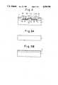
- FIGS. 1, 2, 3 and 4are sectional views schematically illustrating embodiments of the insulated gate FET of the present invention.
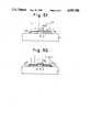
- FIGS. 5A to 5Gare sectional views schematically illustrating a sequence of steps involved in the manufacture of the insulated gate FET of FIG. 1 according to the manufacturing method of the present invention.
- FIGS. 1, 2, 3 and 4illustrate first, second, third and fourth embodiments of the present invention, respectively, in which an island-shaped N- -, P- or I-type non-single-crystal semiconductor layer 2 is formed, for example, 0.7 ⁇ m on, for example, a 1.1 mm thick insulating substrate 1 as of quartz glass.
- the non-single-crystal semiconductor layer 2is constituted of, for instance, amorphous, microcrystalline or polycrystalline silicon.
- the non-single-crystal semiconductor layer 2is doped with a hydrogen or a halogen such as fluorine, as a recombination center neutralizer in an amount of 1 atom% or more.
- the non-single-crystal semiconductor layer 2is deposited over the entire area of its surface with, for example, 1000 ⁇ thick gate insulating film 3 as of silicon nitride.
- a stripe-shaped gate electrode 5Gwhich is formed of, for example, microcrystalline or polycrystalline silicon heavily doped with an N-type impurity such as phosphorus or arsenic, is formed, for instance, 0 3 ⁇ m thick on the gate insulating film 3 in such a manner that the gate insulating film 5G separates the non-single-crystal semiconductor layer 2 into two, as viewed from above.
- source and drain regions 5S and 5Dwhich are doped with an N-type impurity such as phosphorus or arsenic, are formed in regions on both sides of the gate electrode 5G in such a manner to define therebetween a channel region 5C.
- the source and drain regions 5S and 5Dvertically extend past the non-single-crystal semiconductor layer 2 but not down to the substrate 1, as shown in FIGS. 2 and 4.
- the two regions of the non-single-crystal semiconductor layer 2 on both sides of the gate electrode 5G, as viewed from above,have formed therein crystallized regions 6S and 6D which define therebetween a non-crystallized region 6C.
- the crystallized regions 6S and 6Dare formed of a microcrystalline or polycrystalline semiconductor, or a mixture thereof, a mixture of the microcrystalline and/or polycrystalline semiconductor and the amorphous semiconductor, or a single-crystal semiconductor.
- the semiconductor layer 2is constituted of the microcrystalline or polycrystalline semiconductor
- the regions 6S and 6Dare formed of the microcrystalline, polycrystalline or single-crystal semiconductor which has a higher degree of crystallization than does the starting microcrystalline or polycrystalline semiconductor.
- the crystallized regions 6S and 6Dvertically extend past the semiconductor layer 2 down to the insulating substrate 1, for example, as shown in FIGS. 2 and 4.
- the regions 6S and 6Dvertically extend past the semiconductor layer 2 but not down to the insulating substrate 1, as depicted in FIGS. 1 and 3.
- the marginal edges of the regions 6S and 6D on the side of the non-single-crystallized region 6Claterally extend across the source and drain regions 5S and 5D under the gate electrode 5G, as shown in FiG. 1 and 2.
- the abovesaid marginal edges of the regions 6C and 6Dlaterally extend but not across the source and drain regions 5S and 5D, as illustrated in FIGS. 3 and 4.
- the insulating substrate 1has formed thereon an insulating film 7 which covers the semiconductor layer 2, the gate insulating film 3 and the gate electrode 5G.
- the insulating film 7is covered with interconnection layers 9S and 9D which make ohmic contact with the source and drain regions 6S and 6D through holes 8S and 8D made in the insulating film 7. Further, on the insulating film 7 is formed an interconnection layer 8G (not shown) which make ohmic contact with the gate electrode 5G.
- an insulated gate FET of the present inventionwhen it is supplied with a control (gate) voltage across the source and gate regions 5S and 5G via the interconnection layers 8S and 8G in a state in which a DC power source (not shown) in connected across the source and drain regions 5S and 5G via a load (not shown), if the control voltage is higher than a certain threshold voltage which is negative reactive to the side of the gate electrode 5G, or zero or positive, then an N-type channel which extends between the source and drain regions 5S and 5D is formed in the channel region 6C on the side of the gate insulating film 3 and a drain current is caused to flow across the drain region 5D, supplying current to the load.
- a control (gate) voltage across the source and gate regions 5S and 5G via the interconnection layers 8S and 8Gin a state in which a DC power source (not shown) in connected across the source and drain regions 5S and 5G via a load (not shown)
- the control voltageif the control voltage is higher than a
- the insulated gate FET in which the drain current flows when the gate voltage is higher than a certain negative threshold voltageis commonly referred to as a depletion type, and in this case, the drain current flows even if the gate voltage is zero.
- the insulated gate FET which causes the drain current flow when the gate voltage is higher than a certain positive threshold voltageis commonly referred to as an enhancement type.
- the FETWhen the gate voltage is lower than the abovesaid gate voltage, the FET remains in the OFF state and causes substantially no drain current to flow.
- the channel forming region 5C o r non-crystallized region 6Cis doped with the recombination center neutralizer in a required and sufficient amount, and the source and drain regions 5S and 5D and the crystallized regions 6S and 6D are also doped with the recombination center neutralizer.
- the crystallized regions 6S and 6Dconstitute the effective regions of the source and drain regions 5S and 5D.
- the regions 6S and 6Dare lower in resistance than the non-crystallized region 6C. Accordingly, such an excellent OFF characteristic as referred to previously in the "Summary" can be obtained, though not described in detail, and this permits a high-speed ON-OFF operation.
- FIGS. 5A though 5Gillustrate the manufacturing method of the insulated gate FET of the present invention described previously in conjunction with FIG. 1.
- FIG. 5the like parts corresponding to those in FIG. 1 are identified by the same reference numerals and no detailed description thereof will be repeated.
- the manufacturestarts with the preparation of the same substrate 1 as mentioned previously with respect to FIG. 1 (FIG. 5A).
- a non-single-crystal semiconductor layer 2'which contain the recombination center neutralizer in an amount of 1 atom% or more and which will ultimately form the non-single-crystal semiconductor layer 2 and an insulating layer 3' which will ultimately form the gate insulating layer 3, are formed in that order over the entire area of the surface of the substrate 1 by means of, for example, a light plasma CVD process holding the substrate 1 at 250° C., for instance (FIG. 5B).
- the laminate member composed of the non-single-crystal semiconductor layer 2' and the insulating layer 3'is subjected to an etching process which employs a plasma obtainable at room temperature by exciting, for example, a gas mixture of CF 4 and oxygen at a high frequency of, for instance, 13.56 MHz.
- a plasma obtainable at room temperatureby exciting, for example, a gas mixture of CF 4 and oxygen at a high frequency of, for instance, 13.56 MHz.
- the non-single-crystal semiconductor layer 2 and the insulation layer 3, described previously with respect to FIG. 1are formed (FIG. 5C).
- a conductive layer 5G'which will ultimately form the gate electrode 5G mentioned previously with respect to FIG. 1, is formed on the substrate 1 to cover the semiconductor layer 2 and the insulating layer 3. Then a mask layer 15G as of photo resist is formed in a pattern of the gate electrode 5G on the conductive layer 5G' (FIG. 5D).
- the conductive layer 5G'is selectively etched away through the mask layer 15G, forming the abovesaid gate electrode 5G (FIG. 5E).
- regions 5S' and 5D'which will form the activated source and drain regions 5S and 5D by the next step, are formed to leave therebetween the channel forming region 5C described previously in connection with FIG. 1 (FIG. 5F).
- the substrate 1is held below 400° C. so that the recombination center neutralizer doped in the semiconductor layer 2 are not diffused to the outside thereof.
- the mask layer 15Gis removed from the gate electrode 5G, after which the regions 5S' and 5D' are scanned all over them, together with the gate electrode 5G, for example, at a rate of 5 to 50 cm/minute, by light 17 for annealing which is obtainable with, for instance, an ultra-high mercury lamp and which has a wavelength of 250 to 600 nm, a beam diameter of 15 mm and an output of 5 KW.
- the crystallized regions 6S and 6D mentioned previously in conjunction with FIG. 1are formed, and at the same time, the regions 5S' and 5D' are activated, providing the ultimate source and drain regions 5S and 5D (FIG. 5G).
- the crystallized regions 6S and 6D thus obtainedhave a sheet resistance as low as 1 ⁇ 10 2 ( ⁇ cm) -1 when the sheet resistance of the channel forming region is 4 ⁇ 10 -3 ( ⁇ cm) -1 .
- the substrate 1is held below 400° C. so that the recombination center neutralizer doped in the semiconductor layer 2 are not diffused to the outside thereof.
- the light irradiationmay also be effected intermittently with a view to prevent the semiconductor layer 2 from being heated to such a high temperature that causes the diffusion of the recombination center neutralizer to the outside of the layer 2.
- the gate electrode 5Gis a phosphorus-doped non-single-crystallization layer, its degree of crystallization is higher than that before exposure to the light irradiation.
- the substrate 1is coated with the insulating film 7 as depicted in FIG. 1, and then the contact holes 8S, 8D and 8G (the hole 8G being not shown) are made in the insulating film 7.
- the interconnection layers 9S, 9D and 9Gare formed on the insulating film 7 so that they make ohmic contact with the source and drain regions 5S and 5D and the gate electrode 5G through the contact holes 8S, 8D and 8G, respectively
- the drain current obtained during the ON statewas as large as 1 ⁇ 10 -5 to 2 ⁇ 10 -5 (A), whereas during the OFF state it was as small as 10 -10 to 10 -11 (A). Further, since the crystallized regions 6S and 6D laterally extend across the source and drain regions 5S and 5D to underlie the gate electrode 5G, a high avalanche breakdown voltage can be obtained.
- FIG. 1While the foregoing description has been given of the manufacture of the insulated gate FET of the present invention depicted in FIG. 1, it will be seen that the insulated gate FETs of the present invention shown in FIGS. 2, 3 and 4 can also be fabricated by method of the present invention similar to that described above.
Landscapes
- Engineering & Computer Science (AREA)
- Physics & Mathematics (AREA)
- Condensed Matter Physics & Semiconductors (AREA)
- General Physics & Mathematics (AREA)
- Manufacturing & Machinery (AREA)
- Computer Hardware Design (AREA)
- Microelectronics & Electronic Packaging (AREA)
- Power Engineering (AREA)
- Chemical & Material Sciences (AREA)
- Crystallography & Structural Chemistry (AREA)
- High Energy & Nuclear Physics (AREA)
- Materials Engineering (AREA)
- Electromagnetism (AREA)
- Optics & Photonics (AREA)
- Health & Medical Sciences (AREA)
- Toxicology (AREA)
- Thin Film Transistor (AREA)
Abstract
Description
This application is a continuation of Ser. No. 735,697, filed May 20, 1985, now abandoned.
1. Field of the Invention
The present invention relates to an insulated gate field effect transistor (herein after refer to as an insulated gate FET or an FET) and its manufacturing method.
2. Description of the Prior Art
Heretofore there has been proposed an insulated gate FET of the type that it has a high resistivity semiconductor layer formed on a substrate having an insulating surface, a gate electrode formed on the semiconductor layer with a gate insulating layer sandwiched therebetween in a manner to divide the semiconductor into two as viewed from above, and N or P conductivity type source and drain regions formed in the semiconductor layer in a manner to leave a channel forming region between first and second regions on both sides of the gate electrode as viewed from above, the source and drain regions being lower in resistivity than the channel region.
The insulated gate FET of such a construction is called an N-channel type or P-channel type insulated gate FET depending upon whether the source and drain regions are the N or P conductivity type, and it operates in such a manner as follows:
When supplied with a control voltage across the source region and the gate electrode with a DC power source connected across the source and drain regions via a load, the insulated gate FET remains in the OFF state if the control voltage is lower than a certain threshold voltage when the FET is the N-channel type, or if the control voltage is higher than the threshold voltage when the FET is the P-channel type. In this case, substantially no current flow (drain current) is caused in the drain region, supplying no current to the load. In the case where the control voltage is higher than the threshold voltage when the FET is the N-channel type, or where the control voltage is lower than the threshold voltage when the FET is the P-channel type, however, a channel region of the same conductivity type as that of the source and drain regions is formed in the channel forming region to extend between the source and drain regions on the side of the gate insulating layer, and the FET is turned ON to cause the drain current to flow, feeling current to the load
As a modification of the above insulated gate FET has been proposed such a structure that the entire region of the semiconductor layer is formed of a single-crystal semiconductor, and accordingly, the channel forming region, the first and second regions and the source and drain regions formed therein, respectively, are all formed of the single-crystal semiconductor.
With such an insulated gate FET, however, the semiconductor layer cannot be formed on the substrate unless the substrate is made of an insulating or semi-insulating single-crystal semiconductor.
when the semiconductor layer is formed of the single-crystal semiconductor layer, especially when the channel forming region is formed of the single-crystal semiconductor, it has a smaller optical energy gap than does it when formed of a non-single-crystal semiconductor. For example, when the semiconductor layer is made of the single-crystal silicon, the optical energy gap of the channel forming region is 1.1 eV. On account of this, when the FET is in the OFF state, the drain current is small but larger than in the case where the channel forming region is formed of the non-single-crystal semiconductor.
For this reason, the abovesaid insulated gate FET is poorer in the OFF characteristic than in the case where the channel forming region is made of the non-single-crystal semiconductor.
Another modified form of the above insulated gate FET heretofore proposed has such a structure that the entire region of the semiconductor layer is formed of a non-single-crystal semiconductor doped with a recombination center neutralizer.
In the case of such an insulated gate FET, even if the substrate is not made of the insulating or semi-insulating single-crystal semiconductor, and even if the substrate is a metallic substrate which has an insulated surface, or such as a glass, ceramic, organic synthetic resin or like insulating material substrate, the semiconductor layer can be formed on the substrate. Further, since the channel forming region is made of the non-single-crystal semiconductor doped with a recombination center neutralizer, it has a larger optical energy gap than in the case where it is formed of the single-crystal semiconductor, so long as it is sufficiently doped with the recombination center neutralizer. For instance, when the semiconductor layer is formed of non-single-crystal silicon well doped with the recombination center neutralizer, the channel forming region has an optical energy gap in the range of 1.7 to 1.8 eV. In consequence, when the insulated gate FET is in the OFF state, the drain current will be markedly small, negligible as compared with that when the channel forming region is formed of the single-crystal semiconductor. Accordingly, so long as the semiconductor layer is sufficiently doped with the recombination center neutralizer, the FET will exhibit a more excellent OFF characteristic than does it when the channel forming region is made of the single-crystal semiconductor.
In the case of such an insulate gate FET having the semiconductor layer formed of the non-single-crystal semiconductor, impurity-doped regions are formed in the first and second regions, for example, by ion implantation of an N- or P-type impurity, and then the source and drain regions are formed by heat treatment for the activation of the impurity doped in the impurity-doped regions. During the heat treatment, however, the recombination center neutralizer doped in the channel forming region is diffused therefrom to the outside by the heat. Therefore, the channel forming region contains no required and sufficient amount of recombination center neutralizer, and hence has a smaller optical energy gap than the predetermined.
Accordingly, the conventional insulated gate FET with the semiconductor layer formed of the non-single-crystal semiconductor possesses an excellent OFF characteristic as compared with the case where the channel forming region is made of the single-crystal semiconductor, but the OFF characteristic is not fully satisfactory.
Moreover, in the case of the above prior art insulated gate FET of the type having the semiconductor layer formed of the non-single-crystal semiconductor, since the source and drain regions are also obtained by heat treatment, the recombination center neutralizer doped therein is diffused to the outside during the heat treatment. Thus, since the source and drain regions have the same optical energy gap as that of the channel forming region, there is set up between each of the source and drain regions and the channel forming region substantially no or very small potential barrier against carriers flowing from the source or drain regions toward the channel forming region.
This is another cause of the unsatisfactory OFF characteristic of the conventional insulated gate FET which has the semiconductor layer formed of the non-single-crystal semiconductor.
Besides, when the semiconductor layer, and accordingly the source and drain regions are formed of the non-single-crystal semiconductor, they has the same degree of crystallization as that of the channel forming region and a far higher resistance than in the case where they are made of the single-crystal semiconductor. On account of this, in the conventional insulated gate FET of the type having the semiconductor layer formed of the non-single-crystal semiconductor, the speed of switching between the ON and the OFF state is lower than in the case where the source and drain regions are formed of the single-crystal semiconductor. Accordingly, this FET has the defect that its ON-OFF operation cannot be achieved at high speed.
It is therefore an object of the present invention to provide a novel insulated gate FET which is free from the abovesaid defects of the prior art.
Another object of the present invention is to provide a novel method for the manufacture of such a novel insulated gate FET.
The insulated gate FET of the present invention has also the same structure as the above-described conventional insulated gate FET. That is, it has a high resistivity semiconductor layer formed on a substrate having an insulating surface, a gate electrode formed on the semiconductor layer with a gate insulating layer sandwiched therebetween so that it separates the semiconductor layer into two as viewed from above, and N or P conductivity type source and drain regions formed in the semiconductor layer so that they define a channel forming region between first and second regions on both sides of the gate electrode as viewed from above and extend vertically from the upper surface of the first and second regions toward the substrate, the source and drain regions having a lower resistivity than that of the channel forming region.
In the insulated gate FET of the present invention, however, the semiconductor layer is formed of a non-single-crystal semiconductor doped with a required and sufficient amount of recombination center neutralizer, and accordingly, the channel forming region is also formed of such a non-single-crystal semiconductor. In the first and second regions which constitute the source and drain regions in the semiconductor layer, there are provided on the sides of the source and drain regions, respectively, crystallized regions which have a higher degree of crystallization than the channel forming region and are doped with the recombination center neutralizer.
The insulated gate FET of the present invention is identical in construction with the aforesaid conventional insulated gage FET which has the semiconductor layer formed of the non-single-crystal semiconductor, except the inclusion of the abovesaid crystallized regions in the semiconductor layer.
Accordingly, the insulated gate FET of the present invention also operates in the same manner as the aforementioned conventional FET. That is, when supplied with a control voltage across the source region and the gate electrode with the power source connected across the source and drain regions via a load, it remains in the OFF state and causes no current flow to the load if the control voltage is lower (or higher) than a certain threshold voltage, and if the control voltage is higher (or lower) than the threshold voltage, it is turned ON to cause drain current to flow, supplying current to the load.
The insulated gate FET of the present invention has also the semiconductor layer forced of the non-single-crystal semiconductor, and hence it is free from the requirement that the substrate be an insulating or semi-insulating single-crystal semiconductor, as is the case with the conventional FET of this kind.
Further, since the semiconductor layer, and consequently the channel forming region is constituted of the non-single-crystal semiconductor doped with the recombination center neutralizer, the insulated gate FET of the present invention exhibits an excellent OFF characteristic over the FET in which the channel forming region is made of the single-crystal semiconductor.
In the insulated gate FET of the present invention, however, the channel forming region is doped with a required and sufficient amount of recombination center neutralizer, as will be evident from the manufacturing method of the present invention described later. Accordingly, the channel forming region has a predetermined optical energy gap, ensuring to provide an excellent OFF characteristic as compared with that of the conventional FET which has the semiconductor layer formed of the non-single-crystal semiconductor.
Moreover, in the insulated gate FET of the present invention, the crystallized regions, which have a higher degree of crystallization than the channel forming region and are doped with the recombination center neutralizer, are formed in the first and second regions which constitute the source and drain regions, respectively, and the crystallized regions form the effective regions of the source and drain regions. On the other hand, the crystallized regions have a smaller optical energy gap than does the channel forming region. Accordingly, there is established between each of the source and drain regions and the channel forming region a potential barrier against carriers which flow from the source or drain region toward the channel forming region.
This ensures that the FET of the present invention exhibits an excellent OFF characteristic over the conventional FET which has the semiconductor layer formed of the non-single-crystal semiconductor.
Besides, in the insulated gate FET of the present invention, the crystallized regions, which constitute the effective regions of the source and drain regions, are formed in the first and second regions, as mentioned above, and the crystallized regions are far lower in resistance than in the case where the first and second regions are not crystallized. On account of this, the speed at which the FET of the present invention is switched between the ON and OFF state is higher than in the case of the prior art FET which has the semiconductor layer formed of the non-single-crystal semiconductor. In other word, the ON-OFF operation of the FET of the present invention is higher in speed than the ON-OFF operation of the conventional FET.
The insulated gate FET manufacturing method of the present invention includes the following steps.
The manufacture starts with the formation of a non-single-crystal semiconductor layer doped with the recombination center neutralizer on a substrate having an insulating surface.
Next, a gate electrode is formed on the non-single-crystal semiconductor layer with a gate insulating layer sandwiched therebetween in such a manner that the non-single-crystal semiconductor layer is separated into two as viewed from above.
Next, source and drain regions doped with N- or P-type impurity and the recombination center neutralizer are formed in first and second regions of the non-single-crystal semiconductor layer on both sides of the gate electrode, as viewed from above, in such a manner to leave therebetween a channel forming region doped with the recombination center neutralizer.
Next, the first and second regions of the non-single-crystal semiconductor layer are exposed to irradiation by light for annealing at a temperature at which the recombination center neutralizer doped in the non-single-crystal semiconductor layer does not substantially diffuse to the outside. By this, the first and second regions of the non-single-crystal semiconductor layer are crystallized to form crystallized regions on the sides of the source and drain regions. And the N-type or P-type impurity in the source and drain regions is activated. The crystallized region have a higher degree of crystallization than the channel forming region, are doped with the recombination center neutralizer and extend vertically from the upper surface of the first and second regions toward the substrate. In this instance, it is preferable that the gate insulating layer be formed on the semiconductor layer to cover the entire area of the surface of each of first and second regions before the exposure to the light irradiation for annealing so as to prevent that the recombination center neutralizer diffuse to the outside from the source and drain regions and the crystallized regions. Further, it is preferable that the light irradiation for annealing be performed intermittently so as to prevent that the high-temperature heating of the crystallized regions by the light irradiation will cause unnecessary diffusion from the source and drain regions and the crystallized regions of the recombination center neutralizer to the outside.
With such a manufacturing method of the present invention, it is possible to easily fabricate the insulated gate FET of the present invention which possesses the aforesaid advantages.
Other objects, features and advantages of the present invention will become more fully apparent from the following detailed description taken in conjunction with the accompanying drawings.
FIGS. 1, 2, 3 and 4 are sectional views schematically illustrating embodiments of the insulated gate FET of the present invention; and
FIGS. 5A to 5G are sectional views schematically illustrating a sequence of steps involved in the manufacture of the insulated gate FET of FIG. 1 according to the manufacturing method of the present invention.
FIGS. 1, 2, 3 and 4 illustrate first, second, third and fourth embodiments of the present invention, respectively, in which an island-shaped N- -, P- or I-type non-single-crystal semiconductor layer 2 is formed, for example, 0.7 μm on, for example, a 1.1 mm thick insulatingsubstrate 1 as of quartz glass. The non-single-crystal semiconductor layer 2 is constituted of, for instance, amorphous, microcrystalline or polycrystalline silicon. The non-single-crystal semiconductor layer 2 is doped with a hydrogen or a halogen such as fluorine, as a recombination center neutralizer in an amount of 1 atom% or more. The non-single-crystal semiconductor layer 2 is deposited over the entire area of its surface with, for example, 1000 Å thickgate insulating film 3 as of silicon nitride. A stripe-shapedgate electrode 5G, which is formed of, for example, microcrystalline or polycrystalline silicon heavily doped with an N-type impurity such as phosphorus or arsenic, is formed, for instance, 0 3 μm thick on thegate insulating film 3 in such a manner that thegate insulating film 5G separates the non-single-crystal semiconductor layer 2 into two, as viewed from above. In the non-single-crystal semiconductor layer 2 source anddrain regions gate electrode 5G in such a manner to define therebetween achannel region 5C.
In this instance, the marginal edges of the source anddrain regions channel region 5C laterally extend to positions right under the opposite marginal edges of thegate electrode 5G, as shown in FIGS. 1 and 2, or to the vicinities of the abovesaid positions, as shown in FIGS. 3 and 4. Further, the source anddrain regions crystal semiconductor layer 2 down to the insulatingsubstrate 1, as show n in FIGS. 1 and 3. Alternatively, the source anddrain regions crystal semiconductor layer 2 but not down to thesubstrate 1, as shown in FIGS. 2 and 4.
The two regions of the non-single-crystal semiconductor layer 2 on both sides of thegate electrode 5G, as viewed from above, have formed therein crystallizedregions non-crystallized region 6C.
In this case, when thesemiconductor layer 2 is constituted of an amorphous semiconductor, thecrystallized regions semiconductor layer 2 is constituted of the microcrystalline or polycrystalline semiconductor, theregions
Thecrystallized regions semiconductor layer 2 down to the insulatingsubstrate 1, for example, as shown in FIGS. 2 and 4. Alternatively, theregions semiconductor layer 2 but not down to the insulatingsubstrate 1, as depicted in FIGS. 1 and 3. The marginal edges of theregions region 6C laterally extend across the source anddrain regions gate electrode 5G, as shown in FiG. 1 and 2. Alternatively, the abovesaid marginal edges of theregions drain regions substrate 1 has formed thereon an insulatingfilm 7 which covers thesemiconductor layer 2, thegate insulating film 3 and thegate electrode 5G.
The insulatingfilm 7 is covered withinterconnection layers drain regions holes film 7. Further, on the insulatingfilm 7 is formed an interconnection layer 8G (not shown) which make ohmic contact with thegate electrode 5G.
With such an insulated gate FET of the present invention as described above, when it is supplied with a control (gate) voltage across the source andgate regions drain regions gate electrode 5G, or zero or positive, then an N-type channel which extends between the source anddrain regions channel region 6C on the side of thegate insulating film 3 and a drain current is caused to flow across thedrain region 5D, supplying current to the load. The insulated gate FET in which the drain current flows when the gate voltage is higher than a certain negative threshold voltage is commonly referred to as a depletion type, and in this case, the drain current flows even if the gate voltage is zero. The insulated gate FET which causes the drain current flow when the gate voltage is higher than a certain positive threshold voltage is commonly referred to as an enhancement type.
When the gate voltage is lower than the abovesaid gate voltage, the FET remains in the OFF state and causes substantially no drain current to flow.
Thechannel forming region 5C o rnon-crystallized region 6C is doped with the recombination center neutralizer in a required and sufficient amount, and the source anddrain regions crystallized regions
Thecrystallized regions drain regions regions non-crystallized region 6C. Accordingly, such an excellent OFF characteristic as referred to previously in the "Summary" can be obtained, though not described in detail, and this permits a high-speed ON-OFF operation.
FIGS. 5A though 5G illustrate the manufacturing method of the insulated gate FET of the present invention described previously in conjunction with FIG. 1. In FIG. 5, the like parts corresponding to those in FIG. 1 are identified by the same reference numerals and no detailed description thereof will be repeated.
The manufacture starts with the preparation of thesame substrate 1 as mentioned previously with respect to FIG. 1 (FIG. 5A).
In the next step, a non-single-crystal semiconductor layer 2' which contain the recombination center neutralizer in an amount of 1 atom% or more and which will ultimately form the non-single-crystal semiconductor layer 2 and an insulating layer 3' which will ultimately form thegate insulating layer 3, are formed in that order over the entire area of the surface of thesubstrate 1 by means of, for example, a light plasma CVD process holding thesubstrate 1 at 250° C., for instance (FIG. 5B). In the formation of the semiconductor layer 2', care should be taken so that oxygen, nitrogen or carbon, which will shorten the carrier lifetime in theultimate layer 2, is not contained therein in a large amount exceeding 5×10¹⁸ atom/cm3 in order to obtain a large drain current during the ON state of the ultimate FET and to prevent the introduction of a hysterisis characteristic in the gate voltage-drain current characteristic of the FET.
Next, the laminate member composed of the non-single-crystal semiconductor layer 2' and the insulating layer 3' is subjected to an etching process which employs a plasma obtainable at room temperature by exciting, for example, a gas mixture of CF4 and oxygen at a high frequency of, for instance, 13.56 MHz. By this, the non-single-crystal semiconductor layer 2 and theinsulation layer 3, described previously with respect to FIG. 1 are formed (FIG. 5C).
Next, aconductive layer 5G', which will ultimately form thegate electrode 5G mentioned previously with respect to FIG. 1, is formed on thesubstrate 1 to cover thesemiconductor layer 2 and the insulatinglayer 3. Then amask layer 15G as of photo resist is formed in a pattern of thegate electrode 5G on theconductive layer 5G' (FIG. 5D).
After this, theconductive layer 5G' is selectively etched away through themask layer 15G, forming theabovesaid gate electrode 5G (FIG. 5E).
This is followed by the implantation of an N-type impurity ion, for example, a phosphorus ion, into the non-single-crystal semiconductor layer 2 using the laminate member composed of thegate electrode 5G and themask layer 15G. By this,regions 5S' and 5D', which will form the activated source anddrain regions channel forming region 5C described previously in connection with FIG. 1 (FIG. 5F). In this case, thesubstrate 1 is held below 400° C. so that the recombination center neutralizer doped in thesemiconductor layer 2 are not diffused to the outside thereof.
Next, themask layer 15G is removed from thegate electrode 5G, after which theregions 5S' and 5D' are scanned all over them, together with thegate electrode 5G, for example, at a rate of 5 to 50 cm/minute, bylight 17 for annealing which is obtainable with, for instance, an ultra-high mercury lamp and which has a wavelength of 250 to 600 nm, a beam diameter of 15 mm and an output of 5 KW. By this, thecrystallized regions regions 5S' and 5D' are activated, providing the ultimate source anddrain regions crystallized regions substrate 1 is held below 400° C. so that the recombination center neutralizer doped in thesemiconductor layer 2 are not diffused to the outside thereof. Further, the light irradiation may also be effected intermittently with a view to prevent thesemiconductor layer 2 from being heated to such a high temperature that causes the diffusion of the recombination center neutralizer to the outside of thelayer 2. In this instance, when thegate electrode 5G is a phosphorus-doped non-single-crystallization layer, its degree of crystallization is higher than that before exposure to the light irradiation.
Next, thesubstrate 1 is coated with the insulatingfilm 7 as depicted in FIG. 1, and then the contact holes 8S, 8D and 8G (the hole 8G being not shown) are made in the insulatingfilm 7. After this, the interconnection layers 9S, 9D and 9G are formed on the insulatingfilm 7 so that they make ohmic contact with the source anddrain regions gate electrode 5G through the contact holes 8S, 8D and 8G, respectively
In the manner described above, the insulated gate FET mentioned in connection with FIG. 1 is fabricated.
With the insulated gate FET thus obtained, according to my experiments, the drain current obtained during the ON state was as large as 1×10⁻⁵ to 2×10⁻⁵ (A), whereas during the OFF state it was as small as 10-10 to 10-11 (A). Further, since thecrystallized regions drain regions gate electrode 5G, a high avalanche breakdown voltage can be obtained.
While the foregoing description has been given of the manufacture of the insulated gate FET of the present invention depicted in FIG. 1, it will be seen that the insulated gate FETs of the present invention shown in FIGS. 2, 3 and 4 can also be fabricated by method of the present invention similar to that described above.
It will be apparent that many modifications and variations may be effected without departing from the scope of the novel concepts of the present invention.
Claims (9)
1. An insulated gate field effect transistor comprising:
a non-single-crystalline semiconductor layer formed on a substrate;
a gate electrode formed on a portion of the surface of said semiconductor layer;
a gate insulated film disposed between said gate electrode and said semiconductor layer;
a non-single-crystalline channel region defined within said semiconductor layer just below said gate electrode;
a source region and a drain region which are transformed from and defined within said semiconductor layer immediately adjacent to said channel region in an opposed relation, said source and drain regions being crystallized to a higher degree than that of said channel region by selectively irradiating portions of said semiconductor layer using said gate electrode as a mask.
2. An insulated gate field effect transistor according to claim 1 wherein the source and drain regions are each formed vertically extending toward but not to substrate.
3. An insulated gate field effect transistor according to claim 1 wherein the source and drain regions are each formed extending vertically to the substrate.
4. An insulated gate field effect transistor comprising:
a non-single-crystalline semiconductor layer formed on a substrate;
a gate electrode formed on a portion of the surface of said semiconductor layer;
a gate insulated film disposed between said gate electrode and said semiconductor layer;
a non-single-crystalline channel region defined within said semiconductor layer just below said gate electrode;
a source region and a drain region which are defined within said semiconductor layer immediately adjacent to said channel region, said source and drain regions being formed by selectively irradiating and crystallizing portions of said semiconductor layer with said gate electrode as a mask which prevents said channel region from crystallization.
5. An insulated gate field effect transistor comprising a drain region, a source region and a channel region formed on or within a substrate, said transistor characterized in that said three regions are formed within an amorphous semiconductor region or a microcrystalline semiconductor region, and that, out of said drain, source and channel regions, only said drain region and said source region are recrystallized by irradiating said semiconductor region with a laser beam through a mask overlaid on said channel region, so that said channel region remains substantially amorphous or microcrystalline.
6. An insulated gate field effect transistor according to claim 4 wherein the source and drain regions are each formed vertically extending toward but not to the substrate.
7. An insultated gate field effect transistor according to claim 4 wherein the source and drain regions are each formed extending vertically to the substrate.
8. An insulated gate field effect transistor according to claim 5 wherein the source and drain regions are each formed vertically extending toward but not to the substrate.
9. An insulated gate field effect transistor according to claim 5 wherein the source and drain regions are each formed extending vertically to the substrate.
Priority Applications (8)
| Application Number | Priority Date | Filing Date | Title |
|---|---|---|---|
| US07/987,179US5315132A (en) | 1984-05-18 | 1992-12-08 | Insulated gate field effect transistor |
| US08/054,842US5313077A (en) | 1984-05-18 | 1993-04-30 | Insulated gate field effect transistor and its manufacturing method |
| US08/171,769US6660574B1 (en) | 1984-05-18 | 1993-12-22 | Method of forming a semiconductor device including recombination center neutralizer |
| US08/473,953US5543636A (en) | 1984-05-18 | 1995-06-07 | Insulated gate field effect transistor |
| US08/944,136US6680486B1 (en) | 1984-05-18 | 1997-10-06 | Insulated gate field effect transistor and its manufacturing method |
| US08/947,731US6221701B1 (en) | 1984-05-18 | 1997-10-16 | Insulated gate field effect transistor and its manufacturing method |
| US09/406,794US6635520B1 (en) | 1984-05-18 | 1999-09-28 | Operation method of semiconductor devices |
| US09/406,791US6734499B1 (en) | 1984-05-18 | 1999-09-28 | Operation method of semiconductor devices |
Applications Claiming Priority (6)
| Application Number | Priority Date | Filing Date | Title |
|---|---|---|---|
| JP59100251AJPS60245173A (en) | 1984-05-18 | 1984-05-18 | Insulated gate semiconductor device |
| JP59-100250 | 1984-05-18 | ||
| JP59100250AJPS60245172A (en) | 1984-05-18 | 1984-05-18 | Insulated gate type semiconductor device |
| JP59100252AJPS60245174A (en) | 1984-05-18 | 1984-05-18 | Method for manufacturing insulated gate field effect semiconductor device |
| JP59-100251 | 1984-05-18 | ||
| JP59-100252 | 1984-05-18 |
Related Parent Applications (1)
| Application Number | Title | Priority Date | Filing Date |
|---|---|---|---|
| US73569785AContinuation | 1984-05-18 | 1985-05-20 |
Related Child Applications (2)
| Application Number | Title | Priority Date | Filing Date |
|---|---|---|---|
| US52075690ADivision | 1984-05-18 | 1990-05-09 | |
| US52075690AContinuation | 1984-05-18 | 1990-05-09 |
Publications (1)
| Publication Number | Publication Date |
|---|---|
| US4959700Atrue US4959700A (en) | 1990-09-25 |
Family
ID=27309175
Family Applications (11)
| Application Number | Title | Priority Date | Filing Date |
|---|---|---|---|
| US06/912,498Expired - LifetimeUS4727044A (en) | 1984-05-18 | 1986-09-29 | Method of making a thin film transistor with laser recrystallized source and drain |
| US07/153,477Expired - LifetimeUS4959700A (en) | 1984-05-18 | 1988-02-03 | Insulated gate field effect transistor and its manufacturing method |
| US07/707,178Expired - LifetimeUS5142344A (en) | 1984-05-18 | 1991-05-24 | Insulated gate field effect transistor and its manufacturing method |
| US07/987,179Expired - LifetimeUS5315132A (en) | 1984-05-18 | 1992-12-08 | Insulated gate field effect transistor |
| US08/054,842Expired - LifetimeUS5313077A (en) | 1984-05-18 | 1993-04-30 | Insulated gate field effect transistor and its manufacturing method |
| US08/171,769Expired - Fee RelatedUS6660574B1 (en) | 1984-05-18 | 1993-12-22 | Method of forming a semiconductor device including recombination center neutralizer |
| US08/473,953Expired - Fee RelatedUS5543636A (en) | 1984-05-18 | 1995-06-07 | Insulated gate field effect transistor |
| US08/944,136Expired - Fee RelatedUS6680486B1 (en) | 1984-05-18 | 1997-10-06 | Insulated gate field effect transistor and its manufacturing method |
| US08/947,731Expired - Fee RelatedUS6221701B1 (en) | 1984-05-18 | 1997-10-16 | Insulated gate field effect transistor and its manufacturing method |
| US09/406,794Expired - Fee RelatedUS6635520B1 (en) | 1984-05-18 | 1999-09-28 | Operation method of semiconductor devices |
| US09/406,791Expired - Fee RelatedUS6734499B1 (en) | 1984-05-18 | 1999-09-28 | Operation method of semiconductor devices |
Family Applications Before (1)
| Application Number | Title | Priority Date | Filing Date |
|---|---|---|---|
| US06/912,498Expired - LifetimeUS4727044A (en) | 1984-05-18 | 1986-09-29 | Method of making a thin film transistor with laser recrystallized source and drain |
Family Applications After (9)
| Application Number | Title | Priority Date | Filing Date |
|---|---|---|---|
| US07/707,178Expired - LifetimeUS5142344A (en) | 1984-05-18 | 1991-05-24 | Insulated gate field effect transistor and its manufacturing method |
| US07/987,179Expired - LifetimeUS5315132A (en) | 1984-05-18 | 1992-12-08 | Insulated gate field effect transistor |
| US08/054,842Expired - LifetimeUS5313077A (en) | 1984-05-18 | 1993-04-30 | Insulated gate field effect transistor and its manufacturing method |
| US08/171,769Expired - Fee RelatedUS6660574B1 (en) | 1984-05-18 | 1993-12-22 | Method of forming a semiconductor device including recombination center neutralizer |
| US08/473,953Expired - Fee RelatedUS5543636A (en) | 1984-05-18 | 1995-06-07 | Insulated gate field effect transistor |
| US08/944,136Expired - Fee RelatedUS6680486B1 (en) | 1984-05-18 | 1997-10-06 | Insulated gate field effect transistor and its manufacturing method |
| US08/947,731Expired - Fee RelatedUS6221701B1 (en) | 1984-05-18 | 1997-10-16 | Insulated gate field effect transistor and its manufacturing method |
| US09/406,794Expired - Fee RelatedUS6635520B1 (en) | 1984-05-18 | 1999-09-28 | Operation method of semiconductor devices |
| US09/406,791Expired - Fee RelatedUS6734499B1 (en) | 1984-05-18 | 1999-09-28 | Operation method of semiconductor devices |
Country Status (1)
| Country | Link |
|---|---|
| US (11) | US4727044A (en) |
Cited By (68)
| Publication number | Priority date | Publication date | Assignee | Title |
|---|---|---|---|---|
| US5124766A (en)* | 1989-06-30 | 1992-06-23 | Texas Instruments Incorporated | Filament channel transistor interconnected with a conductor |
| US5142344A (en)* | 1984-05-18 | 1992-08-25 | Semiconductor Energy Laboratory Co., Ltd. | Insulated gate field effect transistor and its manufacturing method |
| US5231297A (en)* | 1989-07-14 | 1993-07-27 | Sanyo Electric Co., Ltd. | Thin film transistor |
| US5242507A (en)* | 1989-04-05 | 1993-09-07 | Boston University | Impurity-induced seeding of polycrystalline semiconductors |
| US5696011A (en)* | 1992-03-25 | 1997-12-09 | Semiconductor Energy Laboratory Co., Ltd. | Method for forming an insulated gate field effect transistor |
| US5744818A (en)* | 1990-10-15 | 1998-04-28 | Semiconductor Energy Lab | Insulated gate field effect semiconductor device |
| US5753542A (en)* | 1985-08-02 | 1998-05-19 | Semiconductor Energy Laboratory Co., Ltd. | Method for crystallizing semiconductor material without exposing it to air |
| US5773327A (en)* | 1993-02-15 | 1998-06-30 | Semiconductor Energy Laboratory Co., Ltd. | Semiconductor device and method of fabricating the same |
| US5821559A (en)* | 1991-02-16 | 1998-10-13 | Semiconductor Energy Laboratory Co., Ltd. | Electric device, matrix device, electro-optical display device, and semiconductor memory having thin-film transistors |
| US5821563A (en)* | 1990-12-25 | 1998-10-13 | Semiconductor Energy Laboratory Co., Ltd. | Semiconductor device free from reverse leakage and throw leakage |
| US5849601A (en)* | 1990-12-25 | 1998-12-15 | Semiconductor Energy Laboratory Co., Ltd. | Electro-optical device and method for manufacturing the same |
| US5859445A (en)* | 1990-11-20 | 1999-01-12 | Semiconductor Energy Laboratory Co., Ltd. | Electro-optical device including thin film transistors having spoiling impurities added thereto |
| US5905555A (en)* | 1990-11-26 | 1999-05-18 | Semiconductor Energy Laboratory Co., Ltd. | Active matrix type electro-optical device having leveling film |
| US5933205A (en)* | 1991-03-26 | 1999-08-03 | Semiconductor Energy Laboratory Co., Ltd. | Electro-optical device and method for driving the same |
| US5946561A (en)* | 1991-03-18 | 1999-08-31 | Semiconductor Energy Laboratory Co., Ltd. | Semiconductor device and method for forming the same |
| US5959312A (en)* | 1996-09-27 | 1999-09-28 | Xerox Corporation | Sensor with doped microcrystalline silicon channel leads with bubble formation protection means |
| US5962870A (en)* | 1991-08-26 | 1999-10-05 | Semiconductor Energy Laboratory Co., Ltd. | Insulated gate field effect semiconductor devices |
| US5962869A (en)* | 1988-09-28 | 1999-10-05 | Semiconductor Energy Laboratory Co., Ltd. | Semiconductor material and method for forming the same and thin film transistor |
| US5985741A (en)* | 1993-02-15 | 1999-11-16 | Semiconductor Energy Laboratory Co., Ltd. | Semiconductor device and method of fabricating the same |
| US6013928A (en)* | 1991-08-23 | 2000-01-11 | Semiconductor Energy Laboratory Co., Ltd. | Semiconductor device having interlayer insulating film and method for forming the same |
| US6028333A (en)* | 1991-02-16 | 2000-02-22 | Semiconductor Energy Laboratory Co., Ltd. | Electric device, matrix device, electro-optical display device, and semiconductor memory having thin-film transistors |
| US6087679A (en)* | 1997-07-23 | 2000-07-11 | Semiconductor Energy Laboratory Co., Ltd. | Semiconductor thin film and semiconductor device |
| US6124155A (en)* | 1991-06-19 | 2000-09-26 | Semiconductor Energy Laboratory Co., Ltd. | Electro-optical device and thin film transistor and method for forming the same |
| US6147375A (en)* | 1992-02-05 | 2000-11-14 | Semiconductor Energy Laboratory Co., Ltd. | Active matrix display device |
| US6198133B1 (en) | 1993-12-03 | 2001-03-06 | Semiconductor Energy Laboratory Company, Ltd. | Electro-optical device having silicon nitride interlayer insulating film |
| US6225152B1 (en) | 1996-01-20 | 2001-05-01 | Semiconductor Energy Laboratory Co., Ltd. | Semiconductor device and fabrication method thereof |
| US6242758B1 (en) | 1994-12-27 | 2001-06-05 | Semiconductor Energy Laboratory Co., Ltd. | Semiconductor device employing resinous material, method of fabricating the same and electrooptical device |
| US6271066B1 (en)* | 1991-03-18 | 2001-08-07 | Semiconductor Energy Laboratory Co., Ltd. | Semiconductor material and method for forming the same and thin film transistor |
| US6316810B1 (en) | 1996-01-19 | 2001-11-13 | Semiconductor Energy Laboratory Co., Ltd. | Display switch with double layered gate insulation and resinous interlayer dielectric |
| US6326642B1 (en) | 1992-05-29 | 2001-12-04 | Semiconductor Energy Laboratory Co., Ltd. | Electric device, matrix device, electro-optical display device, and semiconductor memory having thin-film transistors |
| US6331717B1 (en) | 1993-08-12 | 2001-12-18 | Semiconductor Energy Laboratory Co. Ltd. | Insulated gate semiconductor device and process for fabricating the same |
| US6337731B1 (en) | 1992-04-28 | 2002-01-08 | Semiconductor Energy Laboratory Co., Ltd. | Electro-optical device and method of driving the same |
| US6352883B1 (en) | 1991-02-22 | 2002-03-05 | Semiconductor Energy Laboratory Co., Ltd. | Semiconductor device and method for forming the same |
| US6441399B1 (en) | 1994-04-22 | 2002-08-27 | Semiconductor Energy Laboratory Co., Ltd. | Semiconductor integrated system |
| US20020142525A1 (en)* | 2001-01-26 | 2002-10-03 | Hideto Ohnuma | Method of manufacturing semiconductor device |
| US6465287B1 (en) | 1996-01-27 | 2002-10-15 | Semiconductor Energy Laboratory Co., Ltd. | Method for fabricating a semiconductor device using a metal catalyst and high temperature crystallization |
| US6478263B1 (en) | 1997-01-17 | 2002-11-12 | Semiconductor Energy Laboratory Co., Ltd. | Semiconductor device and its manufacturing method |
| US6500703B1 (en) | 1993-08-12 | 2002-12-31 | Semicondcutor Energy Laboratory Co., Ltd. | Insulated gate semiconductor device and process for fabricating the same |
| US6504174B1 (en) | 1996-01-19 | 2003-01-07 | Semiconductor Energy Laboratory Co., Ltd. | Semiconductor device and method for fabricating the same |
| US20030017659A1 (en)* | 2001-06-26 | 2003-01-23 | Fujitsu Limited | Polysilicon film forming method |
| US6528820B1 (en) | 1996-01-19 | 2003-03-04 | Semiconductor Energy Laboratory Co., Ltd. | Semiconductor device and method of fabricating same |
| US6562672B2 (en)* | 1991-03-18 | 2003-05-13 | Semiconductor Energy Laboratory Co., Ltd. | Semiconductor material and method for forming the same and thin film transistor |
| US6607947B1 (en) | 1990-05-29 | 2003-08-19 | Semiconductor Energy Laboratory Co., Ltd. | Method of manufacturing a semiconductor device with fluorinated layer for blocking alkali ions |
| US6624450B1 (en) | 1992-03-27 | 2003-09-23 | Semiconductor Energy Laboratory Co., Ltd. | Semiconductor device and method for forming the same |
| US20030201442A1 (en)* | 2002-04-24 | 2003-10-30 | Naoki Makita | Semiconductor device and method for fabricating the same |
| US6693681B1 (en) | 1992-04-28 | 2004-02-17 | Semiconductor Energy Laboratory Co., Ltd. | Electro-optical device and method of driving the same |
| US6744069B1 (en)* | 1996-01-19 | 2004-06-01 | Semiconductor Energy Laboratory Co., Ltd. | Semiconductor device and its manufacturing method |
| US6747627B1 (en) | 1994-04-22 | 2004-06-08 | Semiconductor Energy Laboratory Co., Ltd. | Redundancy shift register circuit for driver circuit in active matrix type liquid crystal display device |
| US20050052584A1 (en)* | 1995-03-18 | 2005-03-10 | Semiconductor Energy Laboratory Co., Ltd., A Japan Corporation | Method for producing display - device |
| US20050104065A1 (en)* | 1990-12-25 | 2005-05-19 | Semiconductor Energy Laboratory Co., Ltd. | Semiconductor device and method for forming the same |
| US6960498B2 (en) | 2002-07-04 | 2005-11-01 | Semiconductor Energy Laboratory Co., Ltd. | Doping method, doping apparatus, and control system for doping apparatus |
| US6964890B1 (en) | 1992-03-17 | 2005-11-15 | Semiconductor Energy Laboratory Co., Ltd. | Semiconductor device and method for forming the same |
| US7037811B1 (en) | 1996-01-26 | 2006-05-02 | Semiconductor Energy Laboratory Co., Ltd. | Method for fabricating a semiconductor device |
| US7056381B1 (en) | 1996-01-26 | 2006-06-06 | Semiconductor Energy Laboratory Co., Ltd. | Fabrication method of semiconductor device |
| US7071041B2 (en) | 2000-01-20 | 2006-07-04 | Semiconductor Energy Laboratory Co., Ltd. | Method of manufacturing a semiconductor device |
| US20060151792A1 (en)* | 1990-11-26 | 2006-07-13 | Semiconductor Energy Laboratory Co., Ltd. | Electro-optical device and driving method for the same |
| US20060177996A1 (en)* | 2005-02-10 | 2006-08-10 | Semiconductor Energy Laboratory Co., Ltd. | Doping method and method of manufacturing field effect transistor |
| US7098479B1 (en) | 1990-12-25 | 2006-08-29 | Semiconductor Energy Laboratory Co., Ltd. | Electro-optical device and method for manufacturing the same |
| US7115902B1 (en) | 1990-11-20 | 2006-10-03 | Semiconductor Energy Laboratory Co., Ltd. | Electro-optical device and method for manufacturing the same |
| US7135741B1 (en) | 1996-03-17 | 2006-11-14 | Semiconductor Energy Laboratory Co., Ltd. | Method of manufacturing a semiconductor device |
| US7205184B2 (en)* | 1997-10-14 | 2007-04-17 | Samsung Electronics Co., Ltd. | Method of crystallizing silicon film and method of manufacturing thin film transistor liquid crystal display |
| US20070252179A1 (en)* | 2006-04-28 | 2007-11-01 | Semiconductor Energy Laboratory Co., Ltd. | Semiconductor device and method for manufacturing the same |
| US7420628B1 (en) | 1991-02-16 | 2008-09-02 | Semiconductor Energy Laboratory Co., Ltd. | Method of making an active-type LCD with digitally graded display |
| US7576360B2 (en) | 1990-12-25 | 2009-08-18 | Semiconductor Energy Laboratory Co., Ltd. | Electro-optical device which comprises thin film transistors and method for manufacturing the same |
| US7709837B2 (en) | 1996-01-19 | 2010-05-04 | Semiconductor Energy Laboratory Co., Ltd | Semiconductor device and its manufacturing method |
| US20110147712A1 (en)* | 2009-12-23 | 2011-06-23 | Marko Radosavljevic | Quantum well transistors with remote counter doping |
| US8106867B2 (en) | 1990-11-26 | 2012-01-31 | Semiconductor Energy Laboratory Co., Ltd. | Electro-optical device and driving method for the same |
| US20120043543A1 (en)* | 2009-04-17 | 2012-02-23 | Sharp Kabushiki Kaisha | Semiconductor device and manufacturing method therefor |
Families Citing this family (199)
| Publication number | Priority date | Publication date | Assignee | Title |
|---|---|---|---|---|
| US6664566B1 (en) | 1982-08-24 | 2003-12-16 | Semiconductor Energy Laboratory Co., Ltd. | Photoelectric conversion device and method of making the same |
| US5391893A (en) | 1985-05-07 | 1995-02-21 | Semicoductor Energy Laboratory Co., Ltd. | Nonsingle crystal semiconductor and a semiconductor device using such semiconductor |
| US5468653A (en)* | 1982-08-24 | 1995-11-21 | Semiconductor Energy Laboratory Co., Ltd. | Photoelectric conversion device and method of making the same |
| USRE38727E1 (en) | 1982-08-24 | 2005-04-19 | Semiconductor Energy Laboratory Co., Ltd. | Photoelectric conversion device and method of making the same |
| US6346716B1 (en) | 1982-12-23 | 2002-02-12 | Semiconductor Energy Laboratory Co., Ltd. | Semiconductor material having particular oxygen concentration and semiconductor device comprising the same |
| USRE37441E1 (en) | 1982-08-24 | 2001-11-13 | Semiconductor Energy Laboratory Co., Ltd. | Photoelectric conversion device |
| JPS59115574A (en) | 1982-12-23 | 1984-07-04 | Semiconductor Energy Lab Co Ltd | Photoelectric conversion device manufacturing method |
| US7038238B1 (en) | 1985-05-07 | 2006-05-02 | Semiconductor Energy Laboratory Co., Ltd. | Semiconductor device having a non-single crystalline semiconductor layer |
| DE3685623T2 (en)* | 1985-10-04 | 1992-12-24 | Hosiden Corp | THIN FILM TRANSISTOR AND METHOD FOR THE PRODUCTION THEREOF. |
| JPS62162362A (en)* | 1986-01-10 | 1987-07-18 | Mitsubishi Electric Corp | Mos integrated circuit and manufacture thereof |
| US4994401A (en)* | 1987-01-16 | 1991-02-19 | Hosiden Electronics Co., Ltd. | Method of making a thin film transistor |
| GB2215126B (en)* | 1988-02-19 | 1990-11-14 | Gen Electric Co Plc | Process for manufacturing a thin film transistor |
| NL8801379A (en)* | 1988-05-30 | 1989-12-18 | Imec Inter Uni Micro Electr | METHOD FOR MANUFACTURING A THIN FILM TRANSISTOR AND SUCH A THIN FILM TRANSISTOR |
| US5012314A (en)* | 1989-03-31 | 1991-04-30 | Mitsubishi Denki Kabushiki Kaisha | Liquid crystal display restoring apparatus |
| JPH0391932A (en)* | 1989-09-04 | 1991-04-17 | Canon Inc | Manufacture of semiconductor device |
| JP2695488B2 (en)* | 1989-10-09 | 1997-12-24 | キヤノン株式会社 | Crystal growth method |
| EP0449524B1 (en)* | 1990-03-24 | 1997-05-28 | Canon Kabushiki Kaisha | Optical annealing method for semiconductor layer and method for producing semiconductor device employing the same semiconductor layer |
| JP2700277B2 (en) | 1990-06-01 | 1998-01-19 | 株式会社半導体エネルギー研究所 | Method for manufacturing thin film transistor |
| US6008078A (en)* | 1990-07-24 | 1999-12-28 | Semiconductor Energy Laboratory Co., Ltd. | Method for manufacturing a semiconductor device |
| US5254208A (en)* | 1990-07-24 | 1993-10-19 | Semiconductor Energy Laboratory Co., Ltd. | Method for manufacturing a semiconductor device |
| US5112764A (en)* | 1990-09-04 | 1992-05-12 | North American Philips Corporation | Method for the fabrication of low leakage polysilicon thin film transistors |
| JP2947654B2 (en)* | 1990-10-31 | 1999-09-13 | キヤノン株式会社 | MIS type transistor |
| TW237562B (en) | 1990-11-09 | 1995-01-01 | Semiconductor Energy Res Co Ltd | |
| US6893906B2 (en)* | 1990-11-26 | 2005-05-17 | Semiconductor Energy Laboratory Co., Ltd. | Electro-optical device and driving method for the same |
| TW209895B (en) | 1990-11-26 | 1993-07-21 | Semiconductor Energy Res Co Ltd | |
| KR920010885A (en)* | 1990-11-30 | 1992-06-27 | 카나이 쯔또무 | Thin film semiconductor, manufacturing method and manufacturing apparatus and image processing apparatus |
| US5420048A (en)* | 1991-01-09 | 1995-05-30 | Canon Kabushiki Kaisha | Manufacturing method for SOI-type thin film transistor |
| US5298455A (en)* | 1991-01-30 | 1994-03-29 | Tdk Corporation | Method for producing a non-single crystal semiconductor device |
| US5289030A (en) | 1991-03-06 | 1994-02-22 | Semiconductor Energy Laboratory Co., Ltd. | Semiconductor device with oxide layer |
| USRE36314E (en)* | 1991-03-06 | 1999-09-28 | Semiconductor Energy Laboratory Co., Ltd. | Insulated gate field effect semiconductor devices having a LDD region and an anodic oxide film of a gate electrode |
| JP2873632B2 (en) | 1991-03-15 | 1999-03-24 | 株式会社半導体エネルギー研究所 | Semiconductor device |
| US6713783B1 (en) | 1991-03-15 | 2004-03-30 | Semiconductor Energy Laboratory Co., Ltd. | Compensating electro-optical device including thin film transistors |
| US5104818A (en)* | 1991-04-15 | 1992-04-14 | United Technologies Corporation | Preimplanted N-channel SOI mesa |
| JP3277548B2 (en)* | 1991-05-08 | 2002-04-22 | セイコーエプソン株式会社 | Display board |
| JP2717237B2 (en) | 1991-05-16 | 1998-02-18 | 株式会社 半導体エネルギー研究所 | Insulated gate semiconductor device and method of manufacturing the same |
| US6975296B1 (en)* | 1991-06-14 | 2005-12-13 | Semiconductor Energy Laboratory Co., Ltd. | Electro-optical device and method of driving the same |
| GB9114018D0 (en)* | 1991-06-28 | 1991-08-14 | Philips Electronic Associated | Thin-film transistor manufacture |
| US5650338A (en)* | 1991-08-26 | 1997-07-22 | Semiconductor Energy Laboratory Co., Ltd. | Method for forming thin film transistor |
| JP3315730B2 (en)* | 1991-08-26 | 2002-08-19 | マイクロリス、コーパレイシャン | Piezoresistive semiconductor sensor gauge and method of making same |
| US6979840B1 (en) | 1991-09-25 | 2005-12-27 | Semiconductor Energy Laboratory Co., Ltd. | Thin film transistors having anodized metal film between the gate wiring and drain wiring |
| US5576222A (en)* | 1992-01-27 | 1996-11-19 | Tdk Corp. | Method of making a semiconductor image sensor device |
| US5474949A (en)* | 1992-01-27 | 1995-12-12 | Matsushita Electric Industrial Co., Ltd. | Method of fabricating capacitor or contact for semiconductor device by forming uneven oxide film and reacting silicon with metal containing gas |
| US5668019A (en)* | 1992-01-30 | 1997-09-16 | Mitsubishi Denki Kabushiki Kaisha | Method of fabricating thin film transistor |
| US6709907B1 (en)* | 1992-02-25 | 2004-03-23 | Semiconductor Energy Laboratory Co., Ltd. | Method of fabricating a thin film transistor |
| JP3182893B2 (en)* | 1992-07-10 | 2001-07-03 | ソニー株式会社 | Method for manufacturing thin film transistor |
| CN1196184C (en)* | 1992-07-06 | 2005-04-06 | 株式会社半导体能源研究所 | Semiconductor device and method for forming the same |
| CN1244891C (en) | 1992-08-27 | 2006-03-08 | 株式会社半导体能源研究所 | Active matrix display |
| TW232751B (en)* | 1992-10-09 | 1994-10-21 | Semiconductor Energy Res Co Ltd | Semiconductor device and method for forming the same |
| US6624477B1 (en)* | 1992-10-09 | 2003-09-23 | Semiconductor Energy Laboratory Co., Ltd. | Semiconductor device and method for manufacturing the same |
| US5643801A (en)* | 1992-11-06 | 1997-07-01 | Semiconductor Energy Laboratory Co., Ltd. | Laser processing method and alignment |
| TW226478B (en)* | 1992-12-04 | 1994-07-11 | Semiconductor Energy Res Co Ltd | Semiconductor device and method for manufacturing the same |
| US5403762A (en)* | 1993-06-30 | 1995-04-04 | Semiconductor Energy Laboratory Co., Ltd. | Method of fabricating a TFT |
| US7097712B1 (en) | 1992-12-04 | 2006-08-29 | Semiconductor Energy Laboratory Co., Ltd. | Apparatus for processing a semiconductor |
| US6323071B1 (en) | 1992-12-04 | 2001-11-27 | Semiconductor Energy Laboratory Co., Ltd. | Method for forming a semiconductor device |
| US6410374B1 (en) | 1992-12-26 | 2002-06-25 | Semiconductor Energy Laborartory Co., Ltd. | Method of crystallizing a semiconductor layer in a MIS transistor |
| US6544825B1 (en) | 1992-12-26 | 2003-04-08 | Semiconductor Energy Laboratory Co., Ltd. | Method of fabricating a MIS transistor |
| TW403972B (en)* | 1993-01-18 | 2000-09-01 | Semiconductor Energy Lab | Method of fabricating mis semiconductor device |
| US5982002A (en)* | 1993-01-27 | 1999-11-09 | Seiko Instruments Inc. | Light valve having a semiconductor film and a fabrication process thereof |
| US6997985B1 (en) | 1993-02-15 | 2006-02-14 | Semiconductor Energy Laboratory Co., Ltd. | Semiconductor, semiconductor device, and method for fabricating the same |
| CN1052110C (en)* | 1993-02-15 | 2000-05-03 | 株式会社半导体能源研究所 | Semiconductor, semiconductor device, and method for fabricating the same |
| JP3369244B2 (en)* | 1993-03-12 | 2003-01-20 | 株式会社半導体エネルギー研究所 | Thin film transistor |
| TW241377B (en)* | 1993-03-12 | 1995-02-21 | Semiconductor Energy Res Co Ltd | |
| US5501989A (en)* | 1993-03-22 | 1996-03-26 | Semiconductor Energy Laboratory Co., Ltd. | Method of making semiconductor device/circuit having at least partially crystallized semiconductor layer |
| KR100355938B1 (en) | 1993-05-26 | 2002-12-16 | 가부시키가이샤 한도오따이 에네루기 켄큐쇼 | Semiconductor device manufacturing method |
| KR100186886B1 (en)* | 1993-05-26 | 1999-04-15 | 야마자끼 승페이 | Semiconductor device manufacturing method |
| US6090646A (en) | 1993-05-26 | 2000-07-18 | Semiconductor Energy Laboratory Co., Ltd. | Method for producing semiconductor device |
| TW281786B (en)* | 1993-05-26 | 1996-07-21 | Handotai Energy Kenkyusho Kk | |
| JP3450376B2 (en)* | 1993-06-12 | 2003-09-22 | 株式会社半導体エネルギー研究所 | Method for manufacturing semiconductor device |
| US6713330B1 (en)* | 1993-06-22 | 2004-03-30 | Semiconductor Energy Laboratory Co., Ltd. | Method of fabricating a thin film transistor |
| US5488000A (en)* | 1993-06-22 | 1996-01-30 | Semiconductor Energy Laboratory Co., Ltd. | Method of fabricating a thin film transistor using a nickel silicide layer to promote crystallization of the amorphous silicon layer |
| US5973382A (en)* | 1993-07-12 | 1999-10-26 | Peregrine Semiconductor Corporation | Capacitor on ultrathin semiconductor on insulator |
| US5973363A (en)* | 1993-07-12 | 1999-10-26 | Peregrine Semiconductor Corp. | CMOS circuitry with shortened P-channel length on ultrathin silicon on insulator |
| US5864162A (en)* | 1993-07-12 | 1999-01-26 | Peregrine Seimconductor Corporation | Apparatus and method of making a self-aligned integrated resistor load on ultrathin silicon on sapphire |
| US5863823A (en)* | 1993-07-12 | 1999-01-26 | Peregrine Semiconductor Corporation | Self-aligned edge control in silicon on insulator |
| US5930638A (en)* | 1993-07-12 | 1999-07-27 | Peregrine Semiconductor Corp. | Method of making a low parasitic resistor on ultrathin silicon on insulator |
| KR100333153B1 (en) | 1993-09-07 | 2002-12-05 | 가부시키가이샤 한도오따이 에네루기 켄큐쇼 | Process for fabricating semiconductor device |
| TW297142B (en)* | 1993-09-20 | 1997-02-01 | Handotai Energy Kenkyusho Kk | |
| US5719065A (en) | 1993-10-01 | 1998-02-17 | Semiconductor Energy Laboratory Co., Ltd. | Method for manufacturing semiconductor device with removable spacers |
| JPH07109573A (en)* | 1993-10-12 | 1995-04-25 | Semiconductor Energy Lab Co Ltd | Glass substrate and heat treatment |
| CN100367461C (en)* | 1993-11-05 | 2008-02-06 | 株式会社半导体能源研究所 | Method for manufacturing thin film transistor and electronic device |
| US6897100B2 (en) | 1993-11-05 | 2005-05-24 | Semiconductor Energy Laboratory Co., Ltd. | Method for processing semiconductor device apparatus for processing a semiconductor and apparatus for processing semiconductor device |
| TW299897U (en)* | 1993-11-05 | 1997-03-01 | Semiconductor Energy Lab | A semiconductor integrated circuit |
| US5624873A (en)* | 1993-11-12 | 1997-04-29 | The Penn State Research Foundation | Enhanced crystallization of amorphous films |
| US5811326A (en)* | 1994-01-17 | 1998-09-22 | Semiconductor Energy Laboratory Co., Ltd. | Method for manufacturing thin film transistor |
| JP3221473B2 (en)* | 1994-02-03 | 2001-10-22 | 株式会社半導体エネルギー研究所 | Method for manufacturing semiconductor device |
| US6051020A (en)* | 1994-02-09 | 2000-04-18 | Boston Scientific Technology, Inc. | Bifurcated endoluminal prosthesis |
| JP3403812B2 (en)* | 1994-05-31 | 2003-05-06 | 株式会社半導体エネルギー研究所 | Method for manufacturing semiconductor device using thin film transistor |
| US6133620A (en) | 1995-05-26 | 2000-10-17 | Semiconductor Energy Laboratory Co., Ltd. | Semiconductor device and process for fabricating the same |
| US6867432B1 (en)* | 1994-06-09 | 2005-03-15 | Semiconductor Energy Lab | Semiconductor device having SiOxNy gate insulating film |
| JPH07335870A (en)* | 1994-06-14 | 1995-12-22 | Mitsubishi Electric Corp | Semiconductor device and manufacturing method thereof |
| US5898188A (en)* | 1994-07-06 | 1999-04-27 | Semiconductor Energy Laboratory Co., Ltd. | Semiconductor device and method for its fabrication |
| US5614729A (en)* | 1994-07-08 | 1997-03-25 | Hosiden Corporation | Top gate thin-film transistor |
| JP2965283B2 (en)* | 1994-07-13 | 1999-10-18 | ヒュンダイ エレクトロニクス インダストリーズ カムパニー リミテッド | Method for manufacturing thin film transistor |
| KR0135691B1 (en)* | 1994-07-20 | 1998-04-22 | 김주용 | Transistor and fabrication method thereof |
| US5796116A (en)* | 1994-07-27 | 1998-08-18 | Sharp Kabushiki Kaisha | Thin-film semiconductor device including a semiconductor film with high field-effect mobility |
| TW395008B (en)* | 1994-08-29 | 2000-06-21 | Semiconductor Energy Lab | Semiconductor circuit for electro-optical device and method of manufacturing the same |
| JP3442500B2 (en) | 1994-08-31 | 2003-09-02 | 株式会社半導体エネルギー研究所 | Method for manufacturing semiconductor circuit |
| US6242289B1 (en) | 1995-09-08 | 2001-06-05 | Semiconductor Energy Laboratories Co., Ltd. | Method for producing semiconductor device |
| KR0139573B1 (en)* | 1994-12-26 | 1998-06-15 | 김주용 | Dual channel thin film transistor and its manufacturing method |
| US5814529A (en) | 1995-01-17 | 1998-09-29 | Semiconductor Energy Laboratory Co., Ltd. | Method for producing a semiconductor integrated circuit including a thin film transistor and a capacitor |
| JP3364081B2 (en)* | 1995-02-16 | 2003-01-08 | 株式会社半導体エネルギー研究所 | Method for manufacturing semiconductor device |
| JP3778456B2 (en) | 1995-02-21 | 2006-05-24 | 株式会社半導体エネルギー研究所 | Method for manufacturing insulated gate thin film semiconductor device |
| US5773328A (en)* | 1995-02-28 | 1998-06-30 | Sgs-Thomson Microelectronics, Inc. | Method of making a fully-dielectric-isolated fet |
| JP3675886B2 (en)* | 1995-03-17 | 2005-07-27 | 株式会社半導体エネルギー研究所 | Method for manufacturing thin film semiconductor device |
| JPH08286212A (en)* | 1995-04-14 | 1996-11-01 | Semiconductor Energy Lab Co Ltd | Production of display device |
| US6933182B1 (en)* | 1995-04-20 | 2005-08-23 | Semiconductor Energy Laboratory Co., Ltd. | Method of manufacturing a semiconductor device and manufacturing system thereof |
| KR0164079B1 (en)* | 1995-06-30 | 1998-12-01 | 김주용 | Semiconductor device and manufacturing method |
| US5885884A (en)* | 1995-09-29 | 1999-03-23 | Intel Corporation | Process for fabricating a microcrystalline silicon structure |
| JP3917205B2 (en)* | 1995-11-30 | 2007-05-23 | 株式会社半導体エネルギー研究所 | Method for manufacturing semiconductor device |
| US6391690B2 (en)* | 1995-12-14 | 2002-05-21 | Seiko Epson Corporation | Thin film semiconductor device and method for producing the same |
| KR100440083B1 (en)* | 1996-01-23 | 2004-10-20 | 가부시키가이샤 한도오따이 에네루기 켄큐쇼 | Semiconductor thin film manufacturing method |
| US6331457B1 (en)* | 1997-01-24 | 2001-12-18 | Semiconductor Energy Laboratory., Ltd. Co. | Method for manufacturing a semiconductor thin film |
| JPH09293793A (en)* | 1996-04-26 | 1997-11-11 | Mitsubishi Electric Corp | Semiconductor device having thin film transistor and manufacturing method thereof |
| JPH09298195A (en)* | 1996-05-08 | 1997-11-18 | Mitsubishi Electric Corp | Semiconductor device and manufacturing method thereof |
| CN1053528C (en)* | 1996-05-14 | 2000-06-14 | 电子科技大学 | Narrow forbidden band source leckage range metal oxide semiconductor field effect transistor and integrated circuit |
| US6746905B1 (en) | 1996-06-20 | 2004-06-08 | Kabushiki Kaisha Toshiba | Thin film transistor and manufacturing process therefor |
| KR100253699B1 (en)* | 1996-06-29 | 2000-05-01 | 김영환 | Soi device and its manufacturing method |
| SE9603283D0 (en)* | 1996-09-10 | 1996-09-10 | Astra Ab | New compounds |
| JP3527034B2 (en)* | 1996-09-20 | 2004-05-17 | 株式会社半導体エネルギー研究所 | Semiconductor device |
| JP3607016B2 (en)* | 1996-10-02 | 2005-01-05 | 株式会社半導体エネルギー研究所 | Semiconductor device and manufacturing method thereof, and portable information processing terminal, head mounted display, navigation system, mobile phone, camera, and projector |
| JPH10135475A (en)* | 1996-10-31 | 1998-05-22 | Semiconductor Energy Lab Co Ltd | Semiconductor device and manufacturing method thereof |
| JP3645387B2 (en)* | 1996-12-30 | 2005-05-11 | 株式会社半導体エネルギー研究所 | Semiconductor circuit |
| US5965861A (en)* | 1997-02-07 | 1999-10-12 | Ncr Corporation | Method and apparatus for enhancing security in a self-service checkout terminal |
| US6452211B1 (en) | 1997-06-10 | 2002-09-17 | Semiconductor Energy Laboratory Co., Ltd. | Semiconductor thin film and semiconductor device |
| JPH11307747A (en)* | 1998-04-17 | 1999-11-05 | Nec Corp | Soi substrate and production thereof |
| JP4076648B2 (en) | 1998-12-18 | 2008-04-16 | 株式会社半導体エネルギー研究所 | Semiconductor device |
| JP4008133B2 (en)* | 1998-12-25 | 2007-11-14 | 株式会社半導体エネルギー研究所 | Semiconductor device |
| US8158980B2 (en) | 2001-04-19 | 2012-04-17 | Semiconductor Energy Laboratory Co., Ltd. | Semiconductor device having a pixel matrix circuit that includes a pixel TFT and a storage capacitor |
| JP4202502B2 (en)* | 1998-12-28 | 2008-12-24 | 株式会社半導体エネルギー研究所 | Semiconductor device |
| US5965917A (en)* | 1999-01-04 | 1999-10-12 | Advanced Micro Devices, Inc. | Structure and method of formation of body contacts in SOI MOSFETS to elimate floating body effects |
| US6326219B2 (en) | 1999-04-05 | 2001-12-04 | Ultratech Stepper, Inc. | Methods for determining wavelength and pulse length of radiant energy used for annealing |
| US6319743B1 (en) | 1999-04-14 | 2001-11-20 | Mykrolis Corporation | Method of making thin film piezoresistive sensor |
| US6370502B1 (en)* | 1999-05-27 | 2002-04-09 | America Online, Inc. | Method and system for reduction of quantization-induced block-discontinuities and general purpose audio codec |
| JP4472056B2 (en) | 1999-07-23 | 2010-06-02 | 株式会社半導体エネルギー研究所 | Electroluminescence display device and manufacturing method thereof |
| TW465119B (en) | 1999-07-23 | 2001-11-21 | Semiconductor Energy Lab | EL display device and a method of manufacturing the same |
| US6369434B1 (en) | 1999-07-30 | 2002-04-09 | International Business Machines Corporation | Nitrogen co-implantation to form shallow junction-extensions of p-type metal oxide semiconductor field effect transistors |
| JP4675467B2 (en)* | 1999-09-24 | 2011-04-20 | 東芝モバイルディスプレイ株式会社 | Manufacturing method of semiconductor circuit |
| GB2358081B (en)* | 2000-01-07 | 2004-02-18 | Seiko Epson Corp | A thin-film transistor and a method for maufacturing thereof |
| JP4683688B2 (en) | 2000-03-16 | 2011-05-18 | 株式会社半導体エネルギー研究所 | Method for manufacturing liquid crystal display device |
| US6936485B2 (en)* | 2000-03-27 | 2005-08-30 | Semiconductor Energy Laboratory Co., Ltd. | Method of manufacturing a light emitting device |
| KR100679512B1 (en)* | 2000-05-10 | 2007-02-07 | 엘지.필립스 엘시디 주식회사 | Manufacturing Method of Array Board for Transverse Electric Field Liquid Crystal Display |
| US6875674B2 (en)* | 2000-07-10 | 2005-04-05 | Semiconductor Energy Laboratory Co., Ltd. | Method of manufacturing a semiconductor device with fluorine concentration |
| TWI221645B (en)* | 2001-01-19 | 2004-10-01 | Semiconductor Energy Lab | Method of manufacturing a semiconductor device |
| US7115453B2 (en)* | 2001-01-29 | 2006-10-03 | Semiconductor Energy Laboratory Co., Ltd. | Semiconductor device and manufacturing method of the same |
| JP2002231627A (en)* | 2001-01-30 | 2002-08-16 | Semiconductor Energy Lab Co Ltd | Method for manufacturing photoelectric conversion device |
| US7141822B2 (en)* | 2001-02-09 | 2006-11-28 | Semiconductor Energy Laboratory Co., Ltd. | Semiconductor device and method for manufacturing the same |
| JP4993810B2 (en)* | 2001-02-16 | 2012-08-08 | 株式会社半導体エネルギー研究所 | Method for manufacturing semiconductor device |
| SG160191A1 (en)* | 2001-02-28 | 2010-04-29 | Semiconductor Energy Lab | Semiconductor device and manufacturing method thereof |
| JP4718700B2 (en) | 2001-03-16 | 2011-07-06 | 株式会社半導体エネルギー研究所 | Method for manufacturing semiconductor device |
| US7052943B2 (en)* | 2001-03-16 | 2006-05-30 | Semiconductor Energy Laboratory Co., Ltd. | Method of manufacturing a semiconductor device |
| US6812081B2 (en)* | 2001-03-26 | 2004-11-02 | Semiconductor Energy Laboratory Co.,.Ltd. | Method of manufacturing semiconductor device |
| US6743700B2 (en)* | 2001-06-01 | 2004-06-01 | Semiconductor Energy Laboratory Co., Ltd. | Semiconductor film, semiconductor device and method of their production |
| KR100491142B1 (en)* | 2001-11-20 | 2005-05-24 | 삼성에스디아이 주식회사 | Method for formming thin film transistor |
| US7050878B2 (en) | 2001-11-22 | 2006-05-23 | Semiconductor Energy Laboratory Co., Ltd. | Semiconductror fabricating apparatus |
| JP2003163221A (en)* | 2001-11-28 | 2003-06-06 | Semiconductor Energy Lab Co Ltd | Method for manufacturing semiconductor device |
| US7133737B2 (en) | 2001-11-30 | 2006-11-07 | Semiconductor Energy Laboratory Co., Ltd. | Program for controlling laser apparatus and recording medium for recording program for controlling laser apparatus and capable of being read out by computer |
| TWI267145B (en) | 2001-11-30 | 2006-11-21 | Semiconductor Energy Lab | Manufacturing method for a semiconductor device |
| US7214573B2 (en)* | 2001-12-11 | 2007-05-08 | Semiconductor Energy Laboratory Co., Ltd. | Method of manufacturing a semiconductor device that includes patterning sub-islands |
| JP3992976B2 (en)* | 2001-12-21 | 2007-10-17 | 株式会社半導体エネルギー研究所 | Method for manufacturing semiconductor device |
| JP4030758B2 (en) | 2001-12-28 | 2008-01-09 | 株式会社半導体エネルギー研究所 | Method for manufacturing semiconductor device |
| EP1827026A1 (en)* | 2002-01-18 | 2007-08-29 | Kabushiki Kaisha Toshiba | Video decoding method and apparatus |
| JP3989761B2 (en) | 2002-04-09 | 2007-10-10 | 株式会社半導体エネルギー研究所 | Semiconductor display device |
| US20030194825A1 (en)* | 2002-04-10 | 2003-10-16 | Kam Law | Deposition of gate metallization for active matrix liquid crystal display (AMLCD) applications |
| US7038239B2 (en) | 2002-04-09 | 2006-05-02 | Semiconductor Energy Laboratory Co., Ltd. | Semiconductor element and display device using the same |
| JP3989763B2 (en) | 2002-04-15 | 2007-10-10 | 株式会社半導体エネルギー研究所 | Semiconductor display device |
| TWI270919B (en) | 2002-04-15 | 2007-01-11 | Semiconductor Energy Lab | Display device and method of fabricating the same |
| US7256421B2 (en) | 2002-05-17 | 2007-08-14 | Semiconductor Energy Laboratory, Co., Ltd. | Display device having a structure for preventing the deterioration of a light emitting device |
| JP4112330B2 (en)* | 2002-10-02 | 2008-07-02 | 富士通株式会社 | Manufacturing method of semiconductor device |
| JP2004172331A (en)* | 2002-11-20 | 2004-06-17 | Ushio Inc | Electric conductivity control method |
| TW594999B (en)* | 2002-11-22 | 2004-06-21 | Toppoly Optoelectronics Corp | Structure of thin film transistor array and driving circuits |
| US7374976B2 (en)* | 2002-11-22 | 2008-05-20 | Semiconductor Energy Laboratory Co., Ltd. | Method for fabricating thin film transistor |
| US7807225B2 (en)* | 2003-01-31 | 2010-10-05 | Sharp Laboratories Of America, Inc. | High density plasma non-stoichiometric SiOxNy films |
| US7314785B2 (en) | 2003-10-24 | 2008-01-01 | Semiconductor Energy Laboratory Co., Ltd. | Display device and manufacturing method thereof |
| JP4661065B2 (en)* | 2004-03-22 | 2011-03-30 | セイコーエプソン株式会社 | Complementary organic semiconductor device |
| US7109584B2 (en)* | 2004-11-23 | 2006-09-19 | International Business Machines Corporation | Dendrite growth control circuit |
| TWI283071B (en)* | 2005-01-19 | 2007-06-21 | Au Optronics Corp | Methods of manufacturing a thin film transistor and a display |
| US20060270066A1 (en)* | 2005-04-25 | 2006-11-30 | Semiconductor Energy Laboratory Co., Ltd. | Organic transistor, manufacturing method of semiconductor device and organic transistor |
| US8318554B2 (en)* | 2005-04-28 | 2012-11-27 | Semiconductor Energy Laboratory Co., Ltd. | Method of forming gate insulating film for thin film transistors using plasma oxidation |
| US7364954B2 (en)* | 2005-04-28 | 2008-04-29 | Semiconductor Energy Laboratory Co., Ltd. | Method for manufacturing semiconductor device |
| US7785947B2 (en)* | 2005-04-28 | 2010-08-31 | Semiconductor Energy Laboratory Co., Ltd. | Method for manufacturing semiconductor device comprising the step of forming nitride/oxide by high-density plasma |
| TWI408734B (en) | 2005-04-28 | 2013-09-11 | Semiconductor Energy Lab | Semiconductor device and method of manufacturing same |
| TWI287826B (en)* | 2005-06-30 | 2007-10-01 | Chunghwa Picture Tubes Ltd | Method of forming thin film transistor and method of repairing defects in polysilicon layer |
| KR100739731B1 (en)* | 2005-09-06 | 2007-07-13 | 삼성전자주식회사 | Image processing method and apparatus for printing displayed image |
| WO2007046290A1 (en)* | 2005-10-18 | 2007-04-26 | Semiconductor Energy Laboratory Co., Ltd. | Semiconductor device and manufacturing method thereof |
| US7972943B2 (en)* | 2007-03-02 | 2011-07-05 | Semiconductor Energy Laboratory Co., Ltd. | Manufacturing method of semiconductor device |
| KR101448899B1 (en)* | 2007-06-12 | 2014-10-13 | 가부시키가이샤 한도오따이 에네루기 켄큐쇼 | Capacitor-less memory |
| US7611930B2 (en)* | 2007-08-17 | 2009-11-03 | Semiconductor Energy Laboratory Co., Ltd. | Method of manufacturing display device |
| US9054206B2 (en)* | 2007-08-17 | 2015-06-09 | Semiconductor Energy Laboratory Co., Ltd. | Method for manufacturing semiconductor device |
| US8187956B2 (en)* | 2007-12-03 | 2012-05-29 | Semiconductor Energy Laboratory Co., Ltd. | Method for manufacturing microcrystalline semiconductor film, thin film transistor having microcrystalline semiconductor film, and photoelectric conversion device having microcrystalline semiconductor film |
| US8591650B2 (en)* | 2007-12-03 | 2013-11-26 | Semiconductor Energy Laboratory Co., Ltd. | Method for forming crystalline semiconductor film, method for manufacturing thin film transistor, and method for manufacturing display device |
| TWI378562B (en)* | 2008-01-23 | 2012-12-01 | Ind Tech Res Inst | Microcrystalline silicon thin film transistor and method for manufactruing the same |
| JP5436017B2 (en)* | 2008-04-25 | 2014-03-05 | 株式会社半導体エネルギー研究所 | Semiconductor device |
| CN102077354B (en)* | 2008-06-27 | 2014-08-20 | 株式会社半导体能源研究所 | Thin film transistor, semiconductor device and electronic device |
| CN102165600B (en)* | 2008-09-26 | 2013-09-25 | 株式会社半导体能源研究所 | Photoelectric conversion device and method for manufacturing same |
| EP2370581B1 (en)* | 2008-12-04 | 2016-08-03 | CuRNA, Inc. | Treatment of vascular endothelial growth factor (vegf) related diseases by inhibition of natural antisense transcript to vegf |
| TWI404233B (en)* | 2009-03-31 | 2013-08-01 | Epistar Corp | A photoelectronic element and the manufacturing method thereof |
| JP5709579B2 (en)* | 2010-03-02 | 2015-04-30 | 株式会社半導体エネルギー研究所 | Method for manufacturing microcrystalline semiconductor film |
| TWI512981B (en) | 2010-04-27 | 2015-12-11 | Semiconductor Energy Lab | Method for manufacturing microcrystalline semiconductor film and method for manufacturing semiconductor device |
| US10933693B2 (en) | 2017-01-10 | 2021-03-02 | Direct Scaffold Supply, LP | Caster adapter and methods related thereto |
Citations (4)
| Publication number | Priority date | Publication date | Assignee | Title |
|---|---|---|---|---|
| US4272880A (en)* | 1979-04-20 | 1981-06-16 | Intel Corporation | MOS/SOS Process |
| US4470060A (en)* | 1981-01-09 | 1984-09-04 | Semiconductor Energy Laboratory Co., Ltd. | Liquid crystal display with vertical non-single crystal semiconductor field effect transistors |
| US4476475A (en)* | 1982-11-19 | 1984-10-09 | Northern Telecom Limited | Stacked MOS transistor |
| US4598304A (en)* | 1981-07-08 | 1986-07-01 | Agency Of Industrial Science & Technology | Thin film devices of silicon |
Family Cites Families (106)
| Publication number | Priority date | Publication date | Assignee | Title |
|---|---|---|---|---|
| US2882243A (en) | 1953-12-24 | 1959-04-14 | Union Carbide Corp | Molecular sieve adsorbents |
| NL241272A (en) | 1958-07-14 | |||
| NL293447A (en) | 1962-05-31 | |||
| US3265981A (en) | 1963-12-02 | 1966-08-09 | Hughes Aircraft Co | Thin-film electrical networks with nonresistive feedback arrangement |
| US3304469A (en)* | 1964-03-03 | 1967-02-14 | Rca Corp | Field effect solid state device having a partially insulated electrode |
| US3426422A (en) | 1965-10-23 | 1969-02-11 | Fairchild Camera Instr Co | Method of making stable semiconductor devices |
| US3462422A (en) | 1966-09-26 | 1969-08-19 | Searle & Co | 17 - oxygenated androsta/estra-4,6,8(14)-trien - 3 - ones,dihydro congeners,and intermediates |
| US3999212A (en)* | 1967-03-03 | 1976-12-21 | Hitachi, Ltd. | Field effect semiconductor device having a protective diode |
| US3982912A (en) | 1971-03-31 | 1976-09-28 | Yoshifumi Yatsurugi | Method for preparation of an improved K-A type zeolite and for separation by adsorption polar and non-polar molecules |
| US3785122A (en) | 1972-01-27 | 1974-01-15 | Y Yatsurugi | Process for preparing 4,5a zeolite and method for separating mixtures using same |
| US3969274A (en) | 1974-03-14 | 1976-07-13 | National Distillers And Chemical Corporation | Fixed bed catalyst |
| CA1040321A (en)* | 1974-07-23 | 1978-10-10 | Alfred C. Ipri | Polycrystalline silicon resistive device for integrated circuits and method for making same |
| US4064521A (en) | 1975-07-28 | 1977-12-20 | Rca Corporation | Semiconductor device having a body of amorphous silicon |
| US4196438A (en)* | 1976-09-29 | 1980-04-01 | Rca Corporation | Article and device having an amorphous silicon containing a halogen and method of fabrication |
| US4055884A (en)* | 1976-12-13 | 1977-11-01 | International Business Machines Corporation | Fabrication of power field effect transistors and the resulting structures |
| US4091527A (en) | 1977-03-07 | 1978-05-30 | Rca Corporation | Method for adjusting the leakage current of silicon-on-sapphire insulated gate field effect transistors |
| US4151007A (en) | 1977-10-11 | 1979-04-24 | Bell Telephone Laboratories, Incorporated | Hydrogen annealing process for stabilizing metal-oxide-semiconductor structures |
| US4149904A (en) | 1977-10-21 | 1979-04-17 | Ncr Corporation | Method for forming ion-implanted self-aligned gate structure by controlled ion scattering |
| US4160260A (en) | 1977-11-17 | 1979-07-03 | Rca Corp. | Planar semiconductor devices and method of making the same |
| US4113514A (en)* | 1978-01-16 | 1978-09-12 | Rca Corporation | Method of passivating a semiconductor device by treatment with atomic hydrogen |
| US4236167A (en) | 1978-02-06 | 1980-11-25 | Rca Corporation | Stepped oxide, high voltage MOS transistor with near intrinsic channel regions of different doping levels |
| US4353085A (en)* | 1978-02-27 | 1982-10-05 | Fujitsu Limited | Integrated semiconductor device having insulated gate field effect transistors with a buried insulating film |
| US4485389A (en) | 1978-03-08 | 1984-11-27 | Energy Conversion Devices, Inc. | Amorphous semiconductors equivalent to crystalline semiconductors |
| US4710786A (en) | 1978-03-16 | 1987-12-01 | Ovshinsky Stanford R | Wide band gap semiconductor alloy material |
| US4226898A (en) | 1978-03-16 | 1980-10-07 | Energy Conversion Devices, Inc. | Amorphous semiconductors equivalent to crystalline semiconductors produced by a glow discharge process |
| US4263057A (en)* | 1978-04-19 | 1981-04-21 | Rca Corporation | Method of manufacturing short channel MOS devices |
| JPS54152894A (en)* | 1978-05-23 | 1979-12-01 | Seiko Epson Corp | Liquid crystal display unit |
| JPS54158190A (en) | 1978-06-05 | 1979-12-13 | Yamazaki Shunpei | Semiconductor device and method of fabricating same |
| JPS55663A (en) | 1978-06-19 | 1980-01-07 | Toshiba Corp | Frequency synthesizer |
| JPS5511329A (en) | 1978-07-08 | 1980-01-26 | Shunpei Yamazaki | Semiconductor device |
| JPS5513939A (en) | 1978-07-17 | 1980-01-31 | Shunpei Yamazaki | Photoelectronic conversion semiconductor device |
| US4239554A (en)* | 1978-07-17 | 1980-12-16 | Shunpei Yamazaki | Semiconductor photoelectric conversion device |
| JPS5529154A (en) | 1978-08-23 | 1980-03-01 | Shunpei Yamazaki | Semiconductor device |
| FR2435818A1 (en) | 1978-09-08 | 1980-04-04 | Ibm France | PROCESS FOR INCREASING THE INTERNAL TRAPPING EFFECT OF SEMICONDUCTOR BODIES |
| JPS5550664A (en)* | 1978-10-07 | 1980-04-12 | Shunpei Yamazaki | Semiconductor device and method of fabricating the same |
| JPS5550663A (en)* | 1978-10-07 | 1980-04-12 | Shunpei Yamazaki | Semiconductor device and method of fabricating the same |
| JPS5578524A (en) | 1978-12-10 | 1980-06-13 | Shunpei Yamazaki | Manufacture of semiconductor device |
| JPS5638815A (en)* | 1979-09-07 | 1981-04-14 | Chiyou Lsi Gijutsu Kenkyu Kumiai | Manufacture of semiconductor device |
| US4337902A (en) | 1980-02-01 | 1982-07-06 | Markham Melvin C | Insulation anti-static and blowing machine |
| JPS5713777A (en) | 1980-06-30 | 1982-01-23 | Shunpei Yamazaki | Semiconductor device and manufacture thereof |
| US4523368A (en)* | 1980-03-03 | 1985-06-18 | Raytheon Company | Semiconductor devices and manufacturing methods |
| JPS56135496A (en) | 1980-03-26 | 1981-10-22 | Wakunaga Yakuhin Kk | Flavonoid compound and its preparative method |
| JPS56135968A (en) | 1980-03-27 | 1981-10-23 | Canon Inc | Amorphous silicon thin film transistor and manufacture thereof |
| JPS56135972A (en)* | 1980-03-28 | 1981-10-23 | Chiyou Lsi Gijutsu Kenkyu Kumiai | Manufacture of semiconductor device |
| NL186662C (en)* | 1980-04-29 | 1992-03-16 | Philips Nv | METHOD FOR MANUFACTURING A SEMICONDUCTOR DEVICE |
| JPS577924A (en) | 1980-06-18 | 1982-01-16 | Hitachi Ltd | Semiconductor device and manufacture thereof |
| JPS5711351A (en)* | 1980-06-25 | 1982-01-21 | Shunpei Yamazaki | Electrostatic copying machine |
| US4889782A (en)* | 1980-06-25 | 1989-12-26 | Semiconductor Energy Laboratory Co., Ltd. | Electrostatic photocopying machine |
| US4889783A (en)* | 1980-06-25 | 1989-12-26 | Semiconductor Energy Laboratory Co., Ltd. | Printing member for electrostatic photocopying |
| US5859443A (en) | 1980-06-30 | 1999-01-12 | Semiconductor Energy Laboratory Co., Ltd. | Semiconductor device |
| JPS5635423A (en)* | 1980-08-04 | 1981-04-08 | Fujitsu Ltd | Method of correcting photomask by polishing |
| NL187328C (en)* | 1980-12-23 | 1991-08-16 | Philips Nv | METHOD FOR MANUFACTURING A SEMICONDUCTOR DEVICE |
| JPS57110356A (en) | 1980-12-27 | 1982-07-09 | Nordson Kk | Continuous type spray painting system |
| JPS57146561A (en) | 1981-03-05 | 1982-09-10 | Tanaka Shokuhin Kk | Processing of cuttlefish |
| JPS57146562A (en) | 1981-03-06 | 1982-09-10 | Asakura Shoten:Kk | Formed food composed mainly of toasted laver powder |
| JPS57160123A (en) | 1981-03-30 | 1982-10-02 | Hitachi Ltd | Semiconductor device |
| FR2504474A1 (en) | 1981-04-28 | 1982-10-29 | Renault | METHOD AND SYSTEM FOR COLLISION DETECTION AND CONTROL OF SECURITY DEVICES |
| US4459739A (en)* | 1981-05-26 | 1984-07-17 | Northern Telecom Limited | Thin film transistors |
| JPS57210635A (en) | 1981-06-19 | 1982-12-24 | Tokyo Daigaku | Manufacture of semiconductor device |
| US4406709A (en)* | 1981-06-24 | 1983-09-27 | Bell Telephone Laboratories, Incorporated | Method of increasing the grain size of polycrystalline materials by directed energy-beams |
| JPS582073A (en) | 1981-06-29 | 1983-01-07 | Sony Corp | Field effect transistor |
| JPS5814538A (en)* | 1981-07-17 | 1983-01-27 | Fujitsu Ltd | Manufacturing method of semiconductor device |
| JPS5823479A (en)* | 1981-08-05 | 1983-02-12 | Fujitsu Ltd | Manufacture of semiconductor device |
| JPS5826052A (en) | 1981-08-06 | 1983-02-16 | Asahi Glass Co Ltd | Glass body with silicon oxide film to prevent alkali diffusion |
| JP2593639B2 (en) | 1981-08-10 | 1997-03-26 | 株式会社 半導体エネルギー研究所 | Insulated gate field effect semiconductor device |
| JPS5828873A (en) | 1981-08-12 | 1983-02-19 | Semiconductor Energy Lab Co Ltd | Semiconductor device manufacturing method |
| US4464521A (en) | 1981-09-10 | 1984-08-07 | Ashland Oil, Inc. | Curable composition and use thereof |
| US4489478A (en) | 1981-09-29 | 1984-12-25 | Fujitsu Limited | Process for producing a three-dimensional semiconductor device |
| JPS5856409A (en)* | 1981-09-30 | 1983-04-04 | Toshiba Corp | Production of semiconductor device |
| US4460670A (en)* | 1981-11-26 | 1984-07-17 | Canon Kabushiki Kaisha | Photoconductive member with α-Si and C, N or O and dopant |
| DE3146981A1 (en)* | 1981-11-26 | 1983-06-01 | Siemens AG, 1000 Berlin und 8000 München | PHOTOTRANSISTOR IN MOS THICK LAYER TECHNOLOGY, METHOD FOR PRODUCING IT AND METHOD FOR ITS OPERATION. |
| JPS5892218A (en) | 1981-11-28 | 1983-06-01 | Semiconductor Energy Lab Co Ltd | Manufacture of semiconductor device |
| JPS5892217A (en)* | 1981-11-28 | 1983-06-01 | Semiconductor Energy Lab Co Ltd | Manufacture of semiconductor device |
| JPS5893277A (en) | 1981-11-30 | 1983-06-02 | Toshiba Corp | Method for manufacturing thin film semiconductor devices |
| US4528480A (en) | 1981-12-28 | 1985-07-09 | Nippon Telegraph & Telephone | AC Drive type electroluminescent display device |
| US4409805A (en) | 1982-01-28 | 1983-10-18 | Wang Tzu Cheng | Key operated lock |
| JPS58155773A (en)* | 1982-03-11 | 1983-09-16 | Semiconductor Energy Lab Co Ltd | Semiconductor device manufacturing method |
| JPS58155774A (en) | 1982-03-11 | 1983-09-16 | Semiconductor Energy Lab Co Ltd | semiconductor equipment |
| JPS58161380A (en)* | 1982-03-19 | 1983-09-24 | Semiconductor Energy Lab Co Ltd | Semiconductor device |
| JPS58192379A (en) | 1982-05-06 | 1983-11-09 | Seiko Epson Corp | thin film transistor |
| JPS58197775A (en) | 1982-05-13 | 1983-11-17 | Canon Inc | thin film transistor |
| JPH0658966B2 (en)* | 1982-05-17 | 1994-08-03 | キヤノン株式会社 | Semiconductor element |
| JPS58206121A (en) | 1982-05-27 | 1983-12-01 | Toshiba Corp | Manufacture of thin-film semiconductor device |
| JPS58209113A (en) | 1982-05-31 | 1983-12-06 | Semiconductor Energy Lab Co Ltd | Purification of reactive gas for semiconductor |
| US4591892A (en)* | 1982-08-24 | 1986-05-27 | Semiconductor Energy Laboratory Co., Ltd. | Semiconductor photoelectric conversion device |
| JPS5935488A (en) | 1982-08-24 | 1984-02-27 | Semiconductor Energy Lab Co Ltd | Semiconductor device |
| US5043772A (en) | 1985-05-07 | 1991-08-27 | Semiconductor Energy Laboratory Co., Ltd. | Semiconductor photo-electrically-sensitive device |
| US5391893A (en) | 1985-05-07 | 1995-02-21 | Semicoductor Energy Laboratory Co., Ltd. | Nonsingle crystal semiconductor and a semiconductor device using such semiconductor |
| JPS5972182A (en)* | 1982-10-18 | 1984-04-24 | Semiconductor Energy Lab Co Ltd | semiconductor equipment |
| JPS59115574A (en) | 1982-12-23 | 1984-07-04 | Semiconductor Energy Lab Co Ltd | Photoelectric conversion device manufacturing method |
| JPS5935423A (en) | 1982-08-24 | 1984-02-27 | Semiconductor Energy Lab Co Ltd | Manufacture of semiconductor device |
| US4520380A (en) | 1982-09-29 | 1985-05-28 | Sovonics Solar Systems | Amorphous semiconductors equivalent to crystalline semiconductors |
| JPS5972128A (en)* | 1982-10-18 | 1984-04-24 | Semiconductor Energy Lab Co Ltd | Manufacture of semiconductor device |
| JPS59195871A (en)* | 1983-04-20 | 1984-11-07 | Mitsubishi Electric Corp | Manufacture of metal oxide semiconductor field-effect transistor |
| FR2544752B1 (en)* | 1983-04-25 | 1985-07-05 | Commissariat Energie Atomique | METHOD OF AMORPHOUS GROWTH OF A BODY WITH RADIATION CRYSTALLIZATION |
| US4619034A (en)* | 1983-05-02 | 1986-10-28 | Ncr Corporation | Method of making laser recrystallized silicon-on-insulator nonvolatile memory device |
| US5111260A (en) | 1983-06-17 | 1992-05-05 | Texax Instruments Incorporated | Polysilicon FETs |
| JPS6096391A (en) | 1983-10-28 | 1985-05-29 | Shinkawa Ltd | Laser working machine |
| US4611220A (en)* | 1983-11-16 | 1986-09-09 | General Motors Corporation | Junction-MOS power field effect transistor |
| JPS60140897A (en)* | 1983-12-28 | 1985-07-25 | 日本電気株式会社 | Resin insulated multilayer board |
| US4769338A (en)* | 1984-05-14 | 1988-09-06 | Energy Conversion Devices, Inc. | Thin film field effect transistor and method of making same |
| US4727044A (en) | 1984-05-18 | 1988-02-23 | Semiconductor Energy Laboratory Co., Ltd. | Method of making a thin film transistor with laser recrystallized source and drain |
| US4667217A (en)* | 1985-04-19 | 1987-05-19 | Ncr Corporation | Two bit vertically/horizontally integrated memory cell |
| EP0211634B1 (en) | 1985-08-02 | 1994-03-23 | Sel Semiconductor Energy Laboratory Co., Ltd. | Method and apparatus for manufacturing semiconductor devices |
| JPH0776866B2 (en) | 1986-03-27 | 1995-08-16 | 株式会社東芝 | Driving circuit in liquid crystal display device |
| JPH0449269A (en)* | 1990-06-14 | 1992-02-18 | Asahi Denka Kogyo Kk | Optically active pentane derivative |
- 1986
- 1986-09-29USUS06/912,498patent/US4727044A/ennot_activeExpired - Lifetime
- 1988
- 1988-02-03USUS07/153,477patent/US4959700A/ennot_activeExpired - Lifetime
- 1991
- 1991-05-24USUS07/707,178patent/US5142344A/ennot_activeExpired - Lifetime
- 1992
- 1992-12-08USUS07/987,179patent/US5315132A/ennot_activeExpired - Lifetime
- 1993
- 1993-04-30USUS08/054,842patent/US5313077A/ennot_activeExpired - Lifetime
- 1993-12-22USUS08/171,769patent/US6660574B1/ennot_activeExpired - Fee Related
- 1995
- 1995-06-07USUS08/473,953patent/US5543636A/ennot_activeExpired - Fee Related
- 1997
- 1997-10-06USUS08/944,136patent/US6680486B1/ennot_activeExpired - Fee Related
- 1997-10-16USUS08/947,731patent/US6221701B1/ennot_activeExpired - Fee Related
- 1999
- 1999-09-28USUS09/406,794patent/US6635520B1/ennot_activeExpired - Fee Related
- 1999-09-28USUS09/406,791patent/US6734499B1/ennot_activeExpired - Fee Related
Patent Citations (4)
| Publication number | Priority date | Publication date | Assignee | Title |
|---|---|---|---|---|
| US4272880A (en)* | 1979-04-20 | 1981-06-16 | Intel Corporation | MOS/SOS Process |
| US4470060A (en)* | 1981-01-09 | 1984-09-04 | Semiconductor Energy Laboratory Co., Ltd. | Liquid crystal display with vertical non-single crystal semiconductor field effect transistors |
| US4598304A (en)* | 1981-07-08 | 1986-07-01 | Agency Of Industrial Science & Technology | Thin film devices of silicon |
| US4476475A (en)* | 1982-11-19 | 1984-10-09 | Northern Telecom Limited | Stacked MOS transistor |
Cited By (206)
| Publication number | Priority date | Publication date | Assignee | Title |
|---|---|---|---|---|
| US6635520B1 (en) | 1984-05-18 | 2003-10-21 | Semiconductor Energy Laboratory Co., Ltd. | Operation method of semiconductor devices |
| US6221701B1 (en) | 1984-05-18 | 2001-04-24 | Semiconductor Energy Laboratory Co., Ltd. | Insulated gate field effect transistor and its manufacturing method |
| US6734499B1 (en) | 1984-05-18 | 2004-05-11 | Semiconductor Energy Laboratory Co., Ltd. | Operation method of semiconductor devices |
| US5142344A (en)* | 1984-05-18 | 1992-08-25 | Semiconductor Energy Laboratory Co., Ltd. | Insulated gate field effect transistor and its manufacturing method |
| US5313077A (en)* | 1984-05-18 | 1994-05-17 | Semiconductor Energy Laboratory Co., Ltd. | Insulated gate field effect transistor and its manufacturing method |
| US5315132A (en)* | 1984-05-18 | 1994-05-24 | Semiconductor Energy Laboratory Co., Ltd. | Insulated gate field effect transistor |
| US5543636A (en)* | 1984-05-18 | 1996-08-06 | Semiconductor Energy Laboratory Co., Ltd. | Insulated gate field effect transistor |
| US6680486B1 (en) | 1984-05-18 | 2004-01-20 | Semiconductor Energy Laboratory Co., Ltd. | Insulated gate field effect transistor and its manufacturing method |
| US6660574B1 (en)* | 1984-05-18 | 2003-12-09 | Semiconductor Energy Laboratory Co., Ltd. | Method of forming a semiconductor device including recombination center neutralizer |
| US5753542A (en)* | 1985-08-02 | 1998-05-19 | Semiconductor Energy Laboratory Co., Ltd. | Method for crystallizing semiconductor material without exposing it to air |
| US6423586B1 (en) | 1986-08-01 | 2002-07-23 | Semiconductor Energy Laboratory Co., Ltd. | Method for crystallizing semiconductor material without exposing it to air |
| US7435635B2 (en) | 1988-09-28 | 2008-10-14 | Semiconductor Energy Laboratory Co., Ltd. | Method for crystallizing semiconductor material |
| US5962869A (en)* | 1988-09-28 | 1999-10-05 | Semiconductor Energy Laboratory Co., Ltd. | Semiconductor material and method for forming the same and thin film transistor |
| US20050181583A1 (en)* | 1988-09-28 | 2005-08-18 | Semiconductor Energy Laboratory Co., Ltd. | Method for crystallizing semiconductor material |
| US20020025659A1 (en)* | 1988-09-28 | 2002-02-28 | Shunpei Yamazaki | Method for crystallizing semiconductor material without exposing it to air |
| US6881615B2 (en) | 1988-09-28 | 2005-04-19 | Semiconductor Energy Laboratory Co., Ltd. | Method for crystallizing semiconductor material without exposing it to air |
| US5242507A (en)* | 1989-04-05 | 1993-09-07 | Boston University | Impurity-induced seeding of polycrystalline semiconductors |
| US5124766A (en)* | 1989-06-30 | 1992-06-23 | Texas Instruments Incorporated | Filament channel transistor interconnected with a conductor |
| US5231297A (en)* | 1989-07-14 | 1993-07-27 | Sanyo Electric Co., Ltd. | Thin film transistor |
| US6607947B1 (en) | 1990-05-29 | 2003-08-19 | Semiconductor Energy Laboratory Co., Ltd. | Method of manufacturing a semiconductor device with fluorinated layer for blocking alkali ions |
| US7355202B2 (en) | 1990-05-29 | 2008-04-08 | Semiconductor Energy Co., Ltd. | Thin-film transistor |
| US20040031961A1 (en)* | 1990-05-29 | 2004-02-19 | Semiconductor Energy Laboratory Co., Ltd. | Thin-film transistor |
| US20090101910A1 (en)* | 1990-05-29 | 2009-04-23 | Hongyong Zhang | Thin-film transistor |
| US5744818A (en)* | 1990-10-15 | 1998-04-28 | Semiconductor Energy Lab | Insulated gate field effect semiconductor device |
| US6448577B1 (en) | 1990-10-15 | 2002-09-10 | Semiconductor Energy Laboratory Co., Ltd. | Semiconductor device with grain boundaries |
| US6011277A (en)* | 1990-11-20 | 2000-01-04 | Semiconductor Energy Laboratory Co., Ltd. | Gate insulated field effect transistors and method of manufacturing the same |
| US7067844B2 (en) | 1990-11-20 | 2006-06-27 | Semiconductor Energy Laboratory Co., Ltd. | Electro-optical device |
| US6306213B1 (en) | 1990-11-20 | 2001-10-23 | Semiconductor Energy Laboratory Co., Ltd. | Electro-optical device and method for manufacturing the same |
| US6737676B2 (en) | 1990-11-20 | 2004-05-18 | Semiconductor Energy Laboratory Co., Ltd. | Gate insulated field effect transistor and method of manufacturing the same |
| US6281520B1 (en) | 1990-11-20 | 2001-08-28 | Semiconductor Energy Laboratory Co., Ltd. | Gate insulated field effect transistors and method of manufacturing the same |
| US7115902B1 (en) | 1990-11-20 | 2006-10-03 | Semiconductor Energy Laboratory Co., Ltd. | Electro-optical device and method for manufacturing the same |
| US6252249B1 (en) | 1990-11-20 | 2001-06-26 | Semiconductor Energy Laboratory Co., Ltd. | Semiconductor device having crystalline silicon clusters |
| US5859445A (en)* | 1990-11-20 | 1999-01-12 | Semiconductor Energy Laboratory Co., Ltd. | Electro-optical device including thin film transistors having spoiling impurities added thereto |
| US20060151792A1 (en)* | 1990-11-26 | 2006-07-13 | Semiconductor Energy Laboratory Co., Ltd. | Electro-optical device and driving method for the same |
| US8026886B2 (en) | 1990-11-26 | 2011-09-27 | Semiconductor Energy Laboratory Co., Ltd. | Electro-optical device and driving method for the same |
| US5946059A (en)* | 1990-11-26 | 1999-08-31 | Semiconductor Energy Laboratory Co., Ltd. | Electro-optical device and driving method for the same |
| US7154147B1 (en) | 1990-11-26 | 2006-12-26 | Semiconductor Energy Laboratory Co., Ltd. | Electro-optical device and driving method for the same |
| US5905555A (en)* | 1990-11-26 | 1999-05-18 | Semiconductor Energy Laboratory Co., Ltd. | Active matrix type electro-optical device having leveling film |
| US8106867B2 (en) | 1990-11-26 | 2012-01-31 | Semiconductor Energy Laboratory Co., Ltd. | Electro-optical device and driving method for the same |
| US7423290B2 (en) | 1990-11-26 | 2008-09-09 | Semiconductor Energy Laboratory Co., Ltd. | Electro-optical device and driving method for the same |
| US6023075A (en)* | 1990-12-25 | 2000-02-08 | Semiconductor Energy Laboratory Co., Ltd. | Electro-optical device and method for manufacturing the same |
| US7098479B1 (en) | 1990-12-25 | 2006-08-29 | Semiconductor Energy Laboratory Co., Ltd. | Electro-optical device and method for manufacturing the same |
| US7375375B2 (en) | 1990-12-25 | 2008-05-20 | Semiconductor Energy Laboratory Co., Ltd. | Semiconductor device and method for forming the same |
| US7576360B2 (en) | 1990-12-25 | 2009-08-18 | Semiconductor Energy Laboratory Co., Ltd. | Electro-optical device which comprises thin film transistors and method for manufacturing the same |
| US5821563A (en)* | 1990-12-25 | 1998-10-13 | Semiconductor Energy Laboratory Co., Ltd. | Semiconductor device free from reverse leakage and throw leakage |
| US20050104065A1 (en)* | 1990-12-25 | 2005-05-19 | Semiconductor Energy Laboratory Co., Ltd. | Semiconductor device and method for forming the same |
| US20070252149A1 (en)* | 1990-12-25 | 2007-11-01 | Semiconductor Energy Laboratory Co., Ltd. | Semiconductor device and method for forming the same |
| US6838698B1 (en) | 1990-12-25 | 2005-01-04 | Semiconductor Energy Laboratory Co., Ltd. | Semiconductor device having source/channel or drain/channel boundary regions |
| US5849601A (en)* | 1990-12-25 | 1998-12-15 | Semiconductor Energy Laboratory Co., Ltd. | Electro-optical device and method for manufacturing the same |
| US7253437B2 (en) | 1990-12-25 | 2007-08-07 | Semiconductor Energy Laboratory Co., Ltd. | Display device having a thin film transistor |
| US7671827B2 (en)* | 1991-02-16 | 2010-03-02 | Semiconductor Energy Laboratory Co., Ltd. | Electro-optical device |
| US7948569B2 (en) | 1991-02-16 | 2011-05-24 | Semiconductor Energy Laboratory Co., Ltd. | Active matrix type display device |
| US5854494A (en)* | 1991-02-16 | 1998-12-29 | Semiconductor Energy Laboratory Co., Ltd. | Electric device, matrix device, electro-optical display device, and semiconductor memory having thin-film transistors |
| US7701523B2 (en) | 1991-02-16 | 2010-04-20 | Semiconductor Energy Laboratory Co., Ltd | Electro-optical device |
| US7646441B2 (en) | 1991-02-16 | 2010-01-12 | Semiconductor Energy Laboratory Co., Ltd. | Electro-optical display device having thin film transistors including a gate insulating film containing fluorine |
| US5821559A (en)* | 1991-02-16 | 1998-10-13 | Semiconductor Energy Laboratory Co., Ltd. | Electric device, matrix device, electro-optical display device, and semiconductor memory having thin-film transistors |
| US6028333A (en)* | 1991-02-16 | 2000-02-22 | Semiconductor Energy Laboratory Co., Ltd. | Electric device, matrix device, electro-optical display device, and semiconductor memory having thin-film transistors |
| US7420628B1 (en) | 1991-02-16 | 2008-09-02 | Semiconductor Energy Laboratory Co., Ltd. | Method of making an active-type LCD with digitally graded display |
| US6352883B1 (en) | 1991-02-22 | 2002-03-05 | Semiconductor Energy Laboratory Co., Ltd. | Semiconductor device and method for forming the same |
| US6717180B2 (en) | 1991-02-22 | 2004-04-06 | Semiconductor Energy Laboratory Co., Ltd. | Semiconductor device and method for forming the same |
| US6271066B1 (en)* | 1991-03-18 | 2001-08-07 | Semiconductor Energy Laboratory Co., Ltd. | Semiconductor material and method for forming the same and thin film transistor |
| US5946561A (en)* | 1991-03-18 | 1999-08-31 | Semiconductor Energy Laboratory Co., Ltd. | Semiconductor device and method for forming the same |
| US6562672B2 (en)* | 1991-03-18 | 2003-05-13 | Semiconductor Energy Laboratory Co., Ltd. | Semiconductor material and method for forming the same and thin film transistor |
| US7489367B1 (en) | 1991-03-26 | 2009-02-10 | Semiconductor Energy Laboratory, Co., Ltd. | Electro-optical device and method for driving the same |
| US6437367B1 (en) | 1991-03-26 | 2002-08-20 | Semiconductor Energy Laboratory Co., Ltd. | Electro-optical device and method for driving the same |
| US6436815B1 (en) | 1991-03-26 | 2002-08-20 | Semiconductor Energy Laboratory Co., Ltd. | Electro-optical device and method for driving the same |
| US7916232B2 (en) | 1991-03-26 | 2011-03-29 | Semiconductor Energy Laboratory Co., Ltd. | Electro-optical device and method for driving the same |
| US5933205A (en)* | 1991-03-26 | 1999-08-03 | Semiconductor Energy Laboratory Co., Ltd. | Electro-optical device and method for driving the same |
| US20110101362A1 (en)* | 1991-06-19 | 2011-05-05 | Semiconductor Energy Laboratory Co., Ltd. | Electro-optical device and thin film transistor and method for forming the same |
| US6124155A (en)* | 1991-06-19 | 2000-09-26 | Semiconductor Energy Laboratory Co., Ltd. | Electro-optical device and thin film transistor and method for forming the same |
| US20080044962A1 (en)* | 1991-06-19 | 2008-02-21 | Semiconductor Energy Laboratory Co., Ltd. | Electro-optical device and thin film transistor and method for forming the same |
| US6847064B2 (en) | 1991-06-19 | 2005-01-25 | Semiconductor Energy Laboratory Co., Ltd. | Semiconductor device having a thin film transistor |
| US6335213B1 (en) | 1991-06-19 | 2002-01-01 | Semiconductor Energy Laboratory Co., Ltd. | Electro-optical device and thin film transistor and method for forming the same |
| US7507991B2 (en) | 1991-06-19 | 2009-03-24 | Semiconductor Energy Laboratory Co., Ltd. | Electro-optical device and thin film transistor and method for forming the same |
| US6797548B2 (en) | 1991-06-19 | 2004-09-28 | Semiconductor Energy Laboratory Co., Inc. | Electro-optical device and thin film transistor and method for forming the same |
| US6166399A (en)* | 1991-06-19 | 2000-12-26 | Semiconductor Energy Laboratory Co., Ltd. | Active matrix device including thin film transistors |
| US7923311B2 (en) | 1991-06-19 | 2011-04-12 | Semiconductor Energy Laboratory Co., Ltd. | Electro-optical device and thin film transistor and method for forming the same |
| US6756258B2 (en) | 1991-06-19 | 2004-06-29 | Semiconductor Energy Laboratory Co., Ltd. | Method of manufacturing a semiconductor device |
| US20050017243A1 (en)* | 1991-06-19 | 2005-01-27 | Semiconductor Energy Laboratory Co., Ltd. | Electro-optical device and thin film transistor and method for forming the same |
| US6977392B2 (en) | 1991-08-23 | 2005-12-20 | Semiconductor Energy Laboratory Co., Ltd. | Semiconductor display device |
| US6566711B1 (en) | 1991-08-23 | 2003-05-20 | Semiconductor Energy Laboratory Co., Ltd. | Semiconductor device having interlayer insulating film |
| US20060060860A1 (en)* | 1991-08-23 | 2006-03-23 | Semiconductor Energy Laboratory Co., Ltd. | Semiconductor device and method for forming the same |
| US6013928A (en)* | 1991-08-23 | 2000-01-11 | Semiconductor Energy Laboratory Co., Ltd. | Semiconductor device having interlayer insulating film and method for forming the same |
| US6331723B1 (en) | 1991-08-26 | 2001-12-18 | Semiconductor Energy Laboratory Co., Ltd. | Active matrix display device having at least two transistors having LDD region in one pixel |
| US6803600B2 (en) | 1991-08-26 | 2004-10-12 | Semiconductor Energy Laboratory Co., Ltd. | Insulated gate field effect semiconductor devices and method of manufacturing the same |
| US20050098782A1 (en)* | 1991-08-26 | 2005-05-12 | Semiconductor Energy Laboratory Co., Ltd. | Insulated gate field effect semiconductor devices and method of manufacturing the same |
| US5962870A (en)* | 1991-08-26 | 1999-10-05 | Semiconductor Energy Laboratory Co., Ltd. | Insulated gate field effect semiconductor devices |
| US7821011B2 (en) | 1991-08-26 | 2010-10-26 | Semiconductor Energy Laboratory Co., Ltd. | Insulated gate field effect semiconductor devices and method of manufacturing the same |
| US7456427B2 (en) | 1991-08-26 | 2008-11-25 | Semiconductor Energy Laboratory Co., Ltd. | Insulated gate field effect semiconductor devices and method of manufacturing the same |
| US6147375A (en)* | 1992-02-05 | 2000-11-14 | Semiconductor Energy Laboratory Co., Ltd. | Active matrix display device |
| US6476447B1 (en) | 1992-02-05 | 2002-11-05 | Semiconductor Energy Laboratory Co., Ltd. | Active matrix display device including a transistor |
| US7564057B1 (en) | 1992-03-17 | 2009-07-21 | Semiconductor Energy Laboratory Co., Ltd. | Semiconductor device having an aluminum nitride film |
| US6964890B1 (en) | 1992-03-17 | 2005-11-15 | Semiconductor Energy Laboratory Co., Ltd. | Semiconductor device and method for forming the same |
| US6323069B1 (en)* | 1992-03-25 | 2001-11-27 | Semiconductor Energy Laboratory Co., Ltd. | Method of manufacturing a thin film transistor using light irradiation to form impurity regions |
| US6887746B2 (en) | 1992-03-25 | 2005-05-03 | Semiconductor Energy Lab | Insulated gate field effect transistor and method for forming the same |
| US6569724B2 (en) | 1992-03-25 | 2003-05-27 | Semiconductor Energy Laboratory Co., Ltd. | Insulated gate field effect transistor and method for forming the same |
| US5696011A (en)* | 1992-03-25 | 1997-12-09 | Semiconductor Energy Laboratory Co., Ltd. | Method for forming an insulated gate field effect transistor |
| US6624450B1 (en) | 1992-03-27 | 2003-09-23 | Semiconductor Energy Laboratory Co., Ltd. | Semiconductor device and method for forming the same |
| US6337731B1 (en) | 1992-04-28 | 2002-01-08 | Semiconductor Energy Laboratory Co., Ltd. | Electro-optical device and method of driving the same |
| US6693681B1 (en) | 1992-04-28 | 2004-02-17 | Semiconductor Energy Laboratory Co., Ltd. | Electro-optical device and method of driving the same |
| US7554616B1 (en) | 1992-04-28 | 2009-06-30 | Semiconductor Energy Laboratory Co., Ltd. | Electro-optical device and method of driving the same |
| US6326642B1 (en) | 1992-05-29 | 2001-12-04 | Semiconductor Energy Laboratory Co., Ltd. | Electric device, matrix device, electro-optical display device, and semiconductor memory having thin-film transistors |
| US6953713B2 (en) | 1992-05-29 | 2005-10-11 | Semiconductor Energy Laboratory Co., Ltd. | Electric device, matrix device, electro-optical display device and semiconductor memory having thin-film transistors |
| US7223996B2 (en) | 1992-05-29 | 2007-05-29 | Semiconductor Energy Laboratory Co., Ltd. | Electric device, matrix device, electro-optical display device, and semiconductor memory having thin-film transistors |
| US20050214990A1 (en)* | 1992-05-29 | 2005-09-29 | Semiconductor Energy Laboratory Co., Ltd. | Electric device, matrix device, electro-optical display device, and semiconductor memory having thin-film transistors |
| US20010045559A1 (en)* | 1993-02-15 | 2001-11-29 | Shunpei Yamazaki | Semiconductor device and method of fabricating the same |
| US6232621B1 (en) | 1993-02-15 | 2001-05-15 | Semiconductor Energy Laboratory Co., Ltd. | Semiconductor device and method of fabricating the same |
| CN1129961C (en)* | 1993-02-15 | 2003-12-03 | 株式会社半导体能源研究所 | Method for manufacture of semiconductor device |
| US5985741A (en)* | 1993-02-15 | 1999-11-16 | Semiconductor Energy Laboratory Co., Ltd. | Semiconductor device and method of fabricating the same |
| US5773327A (en)* | 1993-02-15 | 1998-06-30 | Semiconductor Energy Laboratory Co., Ltd. | Semiconductor device and method of fabricating the same |
| US6413842B2 (en) | 1993-02-15 | 2002-07-02 | Semiconductor Energy Laboratory Co., Ltd. | Semiconductor device and method of fabricating the same |
| US7952097B2 (en) | 1993-02-15 | 2011-05-31 | Semiconductor Energy Laboratory Co., Ltd. | Semiconductor device and method of fabricating the same |
| US6437366B1 (en) | 1993-08-12 | 2002-08-20 | Semiconductor Energy Laboratory Co., Ltd. | Insulated gate semiconductor device and process for fabricating the same |
| US6500703B1 (en) | 1993-08-12 | 2002-12-31 | Semicondcutor Energy Laboratory Co., Ltd. | Insulated gate semiconductor device and process for fabricating the same |
| US7381598B2 (en) | 1993-08-12 | 2008-06-03 | Semiconductor Energy Laboratory Co., Ltd. | Insulated gate semiconductor device and process for fabricating the same |
| US6331717B1 (en) | 1993-08-12 | 2001-12-18 | Semiconductor Energy Laboratory Co. Ltd. | Insulated gate semiconductor device and process for fabricating the same |
| US6198133B1 (en) | 1993-12-03 | 2001-03-06 | Semiconductor Energy Laboratory Company, Ltd. | Electro-optical device having silicon nitride interlayer insulating film |
| US7812894B2 (en) | 1993-12-03 | 2010-10-12 | Semiconductor Energy Laboratory Co., Ltd. | Electro-optical device and method for manufacturing the same |
| US8223289B2 (en) | 1993-12-03 | 2012-07-17 | Semiconductor Energy Laboratory | Electro-optical device and method for manufacturing the same |
| US7564512B2 (en) | 1993-12-03 | 2009-07-21 | Semiconductor Energy Laboratory Co., Ltd. | Electro-optical device and method for manufacturing the same |
| US8339562B2 (en) | 1993-12-03 | 2012-12-25 | Semiconductor Energy Laboratory Co., Ltd. | Electro-optical device and method for manufacturing the same |
| US7081938B1 (en) | 1993-12-03 | 2006-07-25 | Semiconductor Energy Laboratory Co., Ltd. | Electro-optical device and method for manufacturing the same |
| US20090046049A1 (en)* | 1994-04-22 | 2009-02-19 | Semiconductor Energy Laboratory Co., Ltd. | Redundancy shift register circuit for driver circuit in active matrix type liquid crystal display device |
| US7477222B2 (en) | 1994-04-22 | 2009-01-13 | Semiconductor Energy Laboratory Co., Ltd. | Redundancy shift register circuit for driver circuit in active matrix type liquid crystal display device |
| US8638286B2 (en) | 1994-04-22 | 2014-01-28 | Semiconductor Energy Laboratory Co., Ltd. | Redundancy shift register circuit for driver circuit in active matrix type liquid crystal display device |
| US20050139831A1 (en)* | 1994-04-22 | 2005-06-30 | Semiconductor Energy | Semiconductor integrated circuit |
| US8319720B2 (en) | 1994-04-22 | 2012-11-27 | Semiconductor Energy Laboratory Co., Ltd. | Redundancy shift register circuit for driver circuit in active matrix type liquid crystal display device |
| US20020195634A1 (en)* | 1994-04-22 | 2002-12-26 | Semiconductor Energy Laboratory Co., Ltd. | Semiconductor integrated circuit |
| US6599791B1 (en) | 1994-04-22 | 2003-07-29 | Semiconductor Energy Laboratory Co., Ltd. | Semiconductor integrated circuit |
| US6441399B1 (en) | 1994-04-22 | 2002-08-27 | Semiconductor Energy Laboratory Co., Ltd. | Semiconductor integrated system |
| US6943764B1 (en) | 1994-04-22 | 2005-09-13 | Semiconductor Energy Laboratory Co., Ltd. | Driver circuit for an active matrix display device |
| US7145173B2 (en) | 1994-04-22 | 2006-12-05 | Semiconductor Energy Laboratory Co., Ltd. | Semiconductor integrated circuit |
| US6747627B1 (en) | 1994-04-22 | 2004-06-08 | Semiconductor Energy Laboratory Co., Ltd. | Redundancy shift register circuit for driver circuit in active matrix type liquid crystal display device |
| US7166862B2 (en) | 1994-04-22 | 2007-01-23 | Semiconductor Energy Laboratory Co., Ltd. | Semiconductor integrated circuit |
| US6242758B1 (en) | 1994-12-27 | 2001-06-05 | Semiconductor Energy Laboratory Co., Ltd. | Semiconductor device employing resinous material, method of fabricating the same and electrooptical device |
| US20040183076A1 (en)* | 1994-12-27 | 2004-09-23 | Semiconductor Energy Laboratory Co., Ltd. | Semiconductor device, method of fabricating same, and, electrooptical device |
| US7504660B2 (en) | 1994-12-27 | 2009-03-17 | Semiconductor Energy Laboratory Co., Ltd. | Semiconductor device, method of fabricating same, and, electrooptical device |
| US20050020002A1 (en)* | 1994-12-27 | 2005-01-27 | Semiconductor Energy Laboratory Co., Ltd. | Semiconductor device, method of fabricating same, and, electrooptical device |
| US6429053B1 (en) | 1994-12-27 | 2002-08-06 | Semiconductor Energy Laboratory Co., Ltd. | Semiconductor device method of fabricating same, and, electrooptical device |
| US7468526B2 (en) | 1994-12-27 | 2008-12-23 | Semiconductor Energy Laboratory Co., Ltd. | Semiconductor device, method of fabricating same, and electrooptical device |
| US7462519B2 (en) | 1994-12-27 | 2008-12-09 | Semiconductor Energy Laboratory Co., Ltd. | Semiconductor device, method of fabricating same, and, electrooptical device |
| US20050045884A1 (en)* | 1994-12-27 | 2005-03-03 | Semiconductor Energy Laboratory Co., Ltd. | Semiconductor device, method of fabricating same, and electrooptical device |
| US8466469B2 (en) | 1994-12-27 | 2013-06-18 | Semiconductor Energy Laboratory Co., Ltd. | Semiconductor device having pair of flexible substrates |
| US7776663B2 (en) | 1995-03-18 | 2010-08-17 | Semiconductor Energy Laboratory Co., Ltd. | Semiconductor display devices |
| US20050052584A1 (en)* | 1995-03-18 | 2005-03-10 | Semiconductor Energy Laboratory Co., Ltd., A Japan Corporation | Method for producing display - device |
| US8563979B2 (en) | 1995-03-18 | 2013-10-22 | Semiconductor Energy Laboratory Co., Ltd. | Method for producing display device |
| US8012782B2 (en) | 1995-03-18 | 2011-09-06 | Semiconductor Energy Laboratory Co., Ltd. | Method for producing display device |
| US20100311212A1 (en)* | 1995-03-18 | 2010-12-09 | Semiconductor Energy Laboratory Co., Ltd. | Method for producing display device |
| US7483091B1 (en) | 1995-03-18 | 2009-01-27 | Semiconductor Energy Laboratory Co., Ltd. | Semiconductor display devices |
| US7214555B2 (en) | 1995-03-18 | 2007-05-08 | Semiconductor Energy Laboratory Co., Ltd. | Method for producing display device |
| US7271858B2 (en) | 1995-03-18 | 2007-09-18 | Semiconductor Energy Laboratory Co., Ltd. | Method for producing display-device |
| US6528820B1 (en) | 1996-01-19 | 2003-03-04 | Semiconductor Energy Laboratory Co., Ltd. | Semiconductor device and method of fabricating same |
| US7709837B2 (en) | 1996-01-19 | 2010-05-04 | Semiconductor Energy Laboratory Co., Ltd | Semiconductor device and its manufacturing method |
| US6744069B1 (en)* | 1996-01-19 | 2004-06-01 | Semiconductor Energy Laboratory Co., Ltd. | Semiconductor device and its manufacturing method |
| US7679087B2 (en) | 1996-01-19 | 2010-03-16 | Semiconductor Energy Laboratory Co., Ltd. | Semiconductor active region of TFTs having radial crystal grains through the whole area of the region |
| US7427780B2 (en) | 1996-01-19 | 2008-09-23 | Semiconductor Energy Laboratory Co., Ltd. | Semiconductor device and method of fabricating same |
| US6316810B1 (en) | 1996-01-19 | 2001-11-13 | Semiconductor Energy Laboratory Co., Ltd. | Display switch with double layered gate insulation and resinous interlayer dielectric |
| US7173282B2 (en) | 1996-01-19 | 2007-02-06 | Semiconductor Energy Laboratory Co., Ltd. | Semiconductor device having a crystalline semiconductor film |
| US6528358B1 (en) | 1996-01-19 | 2003-03-04 | Semiconductor Energy Laboratory Co., Ltd. | Semiconductor device and method for fabricating the same |
| US7456056B2 (en) | 1996-01-19 | 2008-11-25 | Semiconductor Energy Laboratory Co., Ltd. | Semiconductor device and method for fabricating the same |
| US20050056843A1 (en)* | 1996-01-19 | 2005-03-17 | Semiconductor Energy Laboratory Co., Ltd. | Semiconductor device and its manufacturing method |
| US6504174B1 (en) | 1996-01-19 | 2003-01-07 | Semiconductor Energy Laboratory Co., Ltd. | Semiconductor device and method for fabricating the same |
| US7078727B2 (en) | 1996-01-19 | 2006-07-18 | Semiconductor Energy Laboratory Co., Ltd. | Semiconductor device and its manufacturing method |
| US6225152B1 (en) | 1996-01-20 | 2001-05-01 | Semiconductor Energy Laboratory Co., Ltd. | Semiconductor device and fabrication method thereof |
| US6541315B2 (en) | 1996-01-20 | 2003-04-01 | Semiconductor Energy Laboratory Co., Ltd. | Semiconductor device and fabrication method thereof |
| US7037811B1 (en) | 1996-01-26 | 2006-05-02 | Semiconductor Energy Laboratory Co., Ltd. | Method for fabricating a semiconductor device |
| US7056381B1 (en) | 1996-01-26 | 2006-06-06 | Semiconductor Energy Laboratory Co., Ltd. | Fabrication method of semiconductor device |
| US7422630B2 (en) | 1996-01-26 | 2008-09-09 | Semiconductor Energy Laboratory Co., Ltd. | Fabrication method of semiconductor device |
| US7141491B2 (en) | 1996-01-26 | 2006-11-28 | Semiconductor Energy Laboratory Co., Ltd. | Method for fabricating a semiconductor device |
| US6465287B1 (en) | 1996-01-27 | 2002-10-15 | Semiconductor Energy Laboratory Co., Ltd. | Method for fabricating a semiconductor device using a metal catalyst and high temperature crystallization |
| US7135741B1 (en) | 1996-03-17 | 2006-11-14 | Semiconductor Energy Laboratory Co., Ltd. | Method of manufacturing a semiconductor device |
| US5959312A (en)* | 1996-09-27 | 1999-09-28 | Xerox Corporation | Sensor with doped microcrystalline silicon channel leads with bubble formation protection means |
| US6478263B1 (en) | 1997-01-17 | 2002-11-12 | Semiconductor Energy Laboratory Co., Ltd. | Semiconductor device and its manufacturing method |
| US7297978B2 (en) | 1997-07-23 | 2007-11-20 | Semiconductor Energy Laboratory Co., Ltd. | Semiconductor thin film and semiconductor device |
| US6087679A (en)* | 1997-07-23 | 2000-07-11 | Semiconductor Energy Laboratory Co., Ltd. | Semiconductor thin film and semiconductor device |
| US20080087894A1 (en)* | 1997-07-23 | 2008-04-17 | Semiconductor Energy Laboratory Co., Ltd. | Semiconductor thin film and semiconductor device |
| US8384084B2 (en) | 1997-07-23 | 2013-02-26 | Semiconductor Energy Laboratory Co., Ltd. | Semiconductor thin film and semiconductor device |
| US20050092997A1 (en)* | 1997-07-23 | 2005-05-05 | Semiconductor Energy Laboratory Co., Ltd. | Semiconductor thin film and semiconductor device |
| US20100295046A1 (en)* | 1997-07-23 | 2010-11-25 | Semiconductor Energy Laboratory Co., Ltd. | Semiconductor thin film and semiconductor device |
| US6822262B2 (en) | 1997-07-23 | 2004-11-23 | Semiconductor Energy Laboratory Co., Ltd. | Semiconductor thin film and semiconductor device |
| US20030102480A1 (en)* | 1997-07-23 | 2003-06-05 | Semiconductor Energy Laboratory Co., Ltd. | Semiconductor thin film and semiconductor device |
| US6495886B1 (en) | 1997-07-23 | 2002-12-17 | Semiconductor Energy Laboratory Co., Ltd. | Semiconductor thin film and semiconductor device |
| US7928438B2 (en) | 1997-07-23 | 2011-04-19 | Semiconductor Energy Laboratory Co., Ltd. | Semiconductor thin film and semiconductor device |
| US7205184B2 (en)* | 1997-10-14 | 2007-04-17 | Samsung Electronics Co., Ltd. | Method of crystallizing silicon film and method of manufacturing thin film transistor liquid crystal display |
| US20060220021A1 (en)* | 2000-01-20 | 2006-10-05 | Semiconductor Energy Laboratory Co., Ltd. | Method of manufacturing a semiconductor device |
| US7429751B2 (en) | 2000-01-20 | 2008-09-30 | Semiconductor Energy Laboratory Co., Ltd. | Method of manufacturing a semiconductor device |
| US7071041B2 (en) | 2000-01-20 | 2006-07-04 | Semiconductor Energy Laboratory Co., Ltd. | Method of manufacturing a semiconductor device |
| US20020142525A1 (en)* | 2001-01-26 | 2002-10-03 | Hideto Ohnuma | Method of manufacturing semiconductor device |
| US20070072350A1 (en)* | 2001-01-26 | 2007-03-29 | Semiconductor Energy Laboratory Co., Ltd. | Method of manufacturing semiconductor device |
| US7361577B2 (en) | 2001-01-26 | 2008-04-22 | Semiconductor Energy Laboratory Co., Ltd. | Method of manufacturing semiconductor device |
| US7151017B2 (en) | 2001-01-26 | 2006-12-19 | Semiconductor Energy Laboratory Co., Ltd. | Method of manufacturing semiconductor device |
| US20030017659A1 (en)* | 2001-06-26 | 2003-01-23 | Fujitsu Limited | Polysilicon film forming method |
| US6692999B2 (en)* | 2001-06-26 | 2004-02-17 | Fujitsu Limited | Polysilicon film forming method |
| US7612375B2 (en)* | 2002-04-24 | 2009-11-03 | Sharp Kabushiki Kaisha | Semiconductor device and method for fabricating the same |
| US20030201442A1 (en)* | 2002-04-24 | 2003-10-30 | Naoki Makita | Semiconductor device and method for fabricating the same |
| US20060005768A1 (en)* | 2002-07-04 | 2006-01-12 | Semiconductor Energy Laboratory Co., Ltd. | Doping method, doping apparatus, and control system for doping apparatus |
| US6960498B2 (en) | 2002-07-04 | 2005-11-01 | Semiconductor Energy Laboratory Co., Ltd. | Doping method, doping apparatus, and control system for doping apparatus |
| US7361912B2 (en) | 2002-07-04 | 2008-04-22 | Semiconductor Energy Laboratory Co., Ltd. | Doping method, doping apparatus, and control system for doping apparatus |
| US7442631B2 (en) | 2005-02-10 | 2008-10-28 | Semiconductor Energy Laboratory Co., Ltd. | Doping method and method of manufacturing field effect transistor |
| US20060177996A1 (en)* | 2005-02-10 | 2006-08-10 | Semiconductor Energy Laboratory Co., Ltd. | Doping method and method of manufacturing field effect transistor |
| US20100187524A1 (en)* | 2006-04-28 | 2010-07-29 | Semiconductor Energy Laboratory Co., Ltd. | Semiconductor device and method for manufacturing the same |
| US7692223B2 (en) | 2006-04-28 | 2010-04-06 | Semiconductor Energy Laboratory Co., Ltd | Semiconductor device and method for manufacturing the same |
| US20070252179A1 (en)* | 2006-04-28 | 2007-11-01 | Semiconductor Energy Laboratory Co., Ltd. | Semiconductor device and method for manufacturing the same |
| US8896049B2 (en) | 2006-04-28 | 2014-11-25 | Semiconductor Energy Laboratory Co., Ltd. | Semiconductor device and method for manufacturing the same |
| US20120043543A1 (en)* | 2009-04-17 | 2012-02-23 | Sharp Kabushiki Kaisha | Semiconductor device and manufacturing method therefor |
| US20110147712A1 (en)* | 2009-12-23 | 2011-06-23 | Marko Radosavljevic | Quantum well transistors with remote counter doping |
Also Published As
| Publication number | Publication date |
|---|---|
| US6680486B1 (en) | 2004-01-20 |
| US5315132A (en) | 1994-05-24 |
| US6221701B1 (en) | 2001-04-24 |
| US6635520B1 (en) | 2003-10-21 |
| US6734499B1 (en) | 2004-05-11 |
| US5313077A (en) | 1994-05-17 |
| US6660574B1 (en) | 2003-12-09 |
| US5142344A (en) | 1992-08-25 |
| US5543636A (en) | 1996-08-06 |
| US4727044A (en) | 1988-02-23 |
Similar Documents
| Publication | Publication Date | Title |
|---|---|---|
| US4959700A (en) | Insulated gate field effect transistor and its manufacturing method | |
| US5512494A (en) | Method for manufacturing a thin film transistor having a forward staggered structure | |
| US4463492A (en) | Method of forming a semiconductor device on insulating substrate by selective amorphosization followed by simultaneous activation and reconversion to single crystal state | |
| US5895957A (en) | Minimum charge FET fabricated on an ultrathin silicon on sapphire wafer | |
| JP4295922B2 (en) | Gas immersion laser annealing method suitable for application in the fabrication of small integrated circuits | |
| US4969031A (en) | Semiconductor devices and method for making the same | |
| EP0139467B1 (en) | Method of manufacturing an insulated-gate field-effect transistor | |
| US4753895A (en) | Method of forming low leakage CMOS device on insulating substrate | |
| US4816893A (en) | Low leakage CMOS/insulator substrate devices and method of forming the same | |
| IE57253B1 (en) | Semiconductor-on-insulator(soi)devices and soi ic fabrication method | |
| US4498224A (en) | Method of manufacturing a MOSFET using accelerated ions to form an amorphous region | |
| US4651182A (en) | Insulated-gate field effect transistor and method of fabricating the same | |
| JPH0817848A (en) | Method of manufacturing MOS power device | |
| US4649626A (en) | Semiconductor on insulator edge doping process using an expanded mask | |
| JPH03194937A (en) | Manufacture of thin film transistor | |
| JP2523019B2 (en) | Field effect type semiconductor device | |
| US4067036A (en) | Junction field effect transistor of vertical type | |
| JP2791420B2 (en) | Method for manufacturing field-effect semiconductor device | |
| JPH06333827A (en) | Crystal growth method and channel formation method for mos transistor | |
| JP3125982B2 (en) | Insulated gate field effect semiconductor device | |
| JP3125981B2 (en) | Insulated gate field effect semiconductor device | |
| US5177029A (en) | Method for manufacturing static induction type semiconductor device enhancement mode power | |
| EP0231656B1 (en) | Silicon semiconductor device | |
| JP3127441B2 (en) | Method for manufacturing insulated gate field effect semiconductor device | |
| JPH0783116B2 (en) | Method for manufacturing semiconductor device |
Legal Events
| Date | Code | Title | Description |
|---|---|---|---|
| AS | Assignment | Owner name:SEMICONDUCTOR ENERGY LABORATORY CO., LTD., JAPAN Free format text:ASSIGNMENT OF ASSIGNORS INTEREST.;ASSIGNOR:YAMAZAKI, SHUNPEI;REEL/FRAME:005178/0801 Effective date:19880229 | |
| STCF | Information on status: patent grant | Free format text:PATENTED CASE | |
| FEPP | Fee payment procedure | Free format text:PAYOR NUMBER ASSIGNED (ORIGINAL EVENT CODE: ASPN); ENTITY STATUS OF PATENT OWNER: LARGE ENTITY | |
| FPAY | Fee payment | Year of fee payment:4 | |
| FPAY | Fee payment | Year of fee payment:8 | |
| FEPP | Fee payment procedure | Free format text:PAYER NUMBER DE-ASSIGNED (ORIGINAL EVENT CODE: RMPN); ENTITY STATUS OF PATENT OWNER: LARGE ENTITY Free format text:PAYOR NUMBER ASSIGNED (ORIGINAL EVENT CODE: ASPN); ENTITY STATUS OF PATENT OWNER: LARGE ENTITY | |
| FPAY | Fee payment | Year of fee payment:12 |