US4956694A - Integrated circuit chip stacking - Google Patents
Integrated circuit chip stackingDownload PDFInfo
- Publication number
- US4956694A US4956694AUS07/267,223US26722388AUS4956694AUS 4956694 AUS4956694 AUS 4956694AUS 26722388 AUS26722388 AUS 26722388AUS 4956694 AUS4956694 AUS 4956694A
- Authority
- US
- United States
- Prior art keywords
- contacts
- lcc
- conductors
- electrical
- electronic
- Prior art date
- Legal status (The legal status is an assumption and is not a legal conclusion. Google has not performed a legal analysis and makes no representation as to the accuracy of the status listed.)
- Expired - Lifetime
Links
Images


Classifications
- H—ELECTRICITY
- H01—ELECTRIC ELEMENTS
- H01L—SEMICONDUCTOR DEVICES NOT COVERED BY CLASS H10
- H01L23/00—Details of semiconductor or other solid state devices
- H01L23/48—Arrangements for conducting electric current to or from the solid state body in operation, e.g. leads, terminal arrangements ; Selection of materials therefor
- H01L23/488—Arrangements for conducting electric current to or from the solid state body in operation, e.g. leads, terminal arrangements ; Selection of materials therefor consisting of soldered or bonded constructions
- H01L23/498—Leads, i.e. metallisations or lead-frames on insulating substrates, e.g. chip carriers
- H01L23/49805—Leads, i.e. metallisations or lead-frames on insulating substrates, e.g. chip carriers the leads being also applied on the sidewalls or the bottom of the substrate, e.g. leadless packages for surface mounting
- H—ELECTRICITY
- H01—ELECTRIC ELEMENTS
- H01L—SEMICONDUCTOR DEVICES NOT COVERED BY CLASS H10
- H01L25/00—Assemblies consisting of a plurality of semiconductor or other solid state devices
- H01L25/03—Assemblies consisting of a plurality of semiconductor or other solid state devices all the devices being of a type provided for in a single subclass of subclasses H10B, H10D, H10F, H10H, H10K or H10N, e.g. assemblies of rectifier diodes
- H01L25/10—Assemblies consisting of a plurality of semiconductor or other solid state devices all the devices being of a type provided for in a single subclass of subclasses H10B, H10D, H10F, H10H, H10K or H10N, e.g. assemblies of rectifier diodes the devices having separate containers
- H01L25/105—Assemblies consisting of a plurality of semiconductor or other solid state devices all the devices being of a type provided for in a single subclass of subclasses H10B, H10D, H10F, H10H, H10K or H10N, e.g. assemblies of rectifier diodes the devices having separate containers the devices being integrated devices of class H10
- H—ELECTRICITY
- H05—ELECTRIC TECHNIQUES NOT OTHERWISE PROVIDED FOR
- H05K—PRINTED CIRCUITS; CASINGS OR CONSTRUCTIONAL DETAILS OF ELECTRIC APPARATUS; MANUFACTURE OF ASSEMBLAGES OF ELECTRICAL COMPONENTS
- H05K1/00—Printed circuits
- H05K1/02—Details
- H05K1/14—Structural association of two or more printed circuits
- H05K1/145—Arrangements wherein electric components are disposed between and simultaneously connected to two planar printed circuit boards, e.g. Cordwood modules
- H—ELECTRICITY
- H01—ELECTRIC ELEMENTS
- H01L—SEMICONDUCTOR DEVICES NOT COVERED BY CLASS H10
- H01L2225/00—Details relating to assemblies covered by the group H01L25/00 but not provided for in its subgroups
- H01L2225/03—All the devices being of a type provided for in the same main group of the same subclass of class H10, e.g. assemblies of rectifier diodes
- H01L2225/10—All the devices being of a type provided for in the same main group of the same subclass of class H10, e.g. assemblies of rectifier diodes the devices having separate containers
- H01L2225/1005—All the devices being of a type provided for in the same main group of the same subclass of class H10, e.g. assemblies of rectifier diodes the devices having separate containers the devices being integrated devices of class H10
- H01L2225/1011—All the devices being of a type provided for in the same main group of the same subclass of class H10, e.g. assemblies of rectifier diodes the devices having separate containers the devices being integrated devices of class H10 the containers being in a stacked arrangement
- H01L2225/1017—All the devices being of a type provided for in the same main group of the same subclass of class H10, e.g. assemblies of rectifier diodes the devices having separate containers the devices being integrated devices of class H10 the containers being in a stacked arrangement the lowermost container comprising a device support
- H01L2225/1029—All the devices being of a type provided for in the same main group of the same subclass of class H10, e.g. assemblies of rectifier diodes the devices having separate containers the devices being integrated devices of class H10 the containers being in a stacked arrangement the lowermost container comprising a device support the support being a lead frame
- H—ELECTRICITY
- H01—ELECTRIC ELEMENTS
- H01L—SEMICONDUCTOR DEVICES NOT COVERED BY CLASS H10
- H01L2225/00—Details relating to assemblies covered by the group H01L25/00 but not provided for in its subgroups
- H01L2225/03—All the devices being of a type provided for in the same main group of the same subclass of class H10, e.g. assemblies of rectifier diodes
- H01L2225/10—All the devices being of a type provided for in the same main group of the same subclass of class H10, e.g. assemblies of rectifier diodes the devices having separate containers
- H01L2225/1005—All the devices being of a type provided for in the same main group of the same subclass of class H10, e.g. assemblies of rectifier diodes the devices having separate containers the devices being integrated devices of class H10
- H01L2225/1011—All the devices being of a type provided for in the same main group of the same subclass of class H10, e.g. assemblies of rectifier diodes the devices having separate containers the devices being integrated devices of class H10 the containers being in a stacked arrangement
- H01L2225/1047—Details of electrical connections between containers
- H01L2225/1064—Electrical connections provided on a side surface of one or more of the containers
- H—ELECTRICITY
- H01—ELECTRIC ELEMENTS
- H01L—SEMICONDUCTOR DEVICES NOT COVERED BY CLASS H10
- H01L2924/00—Indexing scheme for arrangements or methods for connecting or disconnecting semiconductor or solid-state bodies as covered by H01L24/00
- H01L2924/0001—Technical content checked by a classifier
- H01L2924/0002—Not covered by any one of groups H01L24/00, H01L24/00 and H01L2224/00
- H—ELECTRICITY
- H01—ELECTRIC ELEMENTS
- H01L—SEMICONDUCTOR DEVICES NOT COVERED BY CLASS H10
- H01L2924/00—Indexing scheme for arrangements or methods for connecting or disconnecting semiconductor or solid-state bodies as covered by H01L24/00
- H01L2924/15—Details of package parts other than the semiconductor or other solid state devices to be connected
- H01L2924/161—Cap
- H01L2924/1615—Shape
- H01L2924/16195—Flat cap [not enclosing an internal cavity]
- H—ELECTRICITY
- H01—ELECTRIC ELEMENTS
- H01L—SEMICONDUCTOR DEVICES NOT COVERED BY CLASS H10
- H01L2924/00—Indexing scheme for arrangements or methods for connecting or disconnecting semiconductor or solid-state bodies as covered by H01L24/00
- H01L2924/15—Details of package parts other than the semiconductor or other solid state devices to be connected
- H01L2924/161—Cap
- H01L2924/162—Disposition
- H01L2924/1627—Disposition stacked type assemblies, e.g. stacked multi-cavities
Definitions
- the present inventionrelates to the stacking and interconnection of leadless chip carriers (LCCs) containing integrated circuit chips (ICs) to achieve, for example, an increased memory capacity in a memory circuit.
- LCCsleadless chip carriers
- ICsintegrated circuit chips
- PCBsprinted circuit boards
- the PCBsare arranged in a parallel relationship, with each PCB disposed adjacent to and spaced from the other PCBs.
- each PCBis spaced by a distance of about 1/2 inch from any adjacent PCBs or other components.
- the known memory circuit systems described aboveexhibit the disadvantage of taking up a relatively large amount of space, much of which is unused and, thus wasted.
- Such memory systemsas described above, also exhibit the disadvantage of a limited memory capacity when employed in devices having a limited amount of space available for memory.
- many conventional computer systemsare provided with a housing structure in which a limited amount of space is provided for the memory circuit system. Since the number of PCBs comprising the memory circuit system is limited by the size of the space provided therefor, the memory capacity of these memory systems is also limited by such space constraints. That is, the memory capacity of such computer systems has heretofore been greatly dependent upon and limited by the size of the space reserved for the memory circuit PCBs.
- the present inventionprovides a memory circuit system which exhibits improved memory density by employing space between printed circuit boards, which space is normally unused or wasted in conventional memory systems.
- Many embodiments of the present inventionmay be made relatively cheaply and are easy to manufacture, inspect and repair, while at the same time being extremely rugged.
- a plurality of memory ICsare encapsulated within a respective plurality of LCCs.
- the side faces of each LCCare provided with several conductors, each of which extends from the top to the bottom face of the LCC.
- the data signal input and/or output terminalshereinafter "input/output" terminals
- power and ground terminal of each encapsulated ICare electrically connected to these conductors on the sides of the LCCs.
- the conductors connected to the data signal input/output terminals of the ICsare called the data conductors
- the conductor connected to the power terminal of the ICis called the power conductor
- the conductor connected to the ground terminal of the ICis called the ground conductor.
- the LCCsare then stacked, one above the other, with data conductors, power conductors and ground conductors of each LCC in alignment with the respective conductors of the other LCCs in the stack.
- the stack of LCCsis then mechanically and electrically connected together such that the aligned conductors of the stacked LCCs are electrically connected to each other. That is, all of the aligned ground conductors are electrically connected together, all of the aligned power conductors are similarly electrically connected together and all of the aligned data conductors are connected together.
- the resulting deviceis an electrical circuit having a plurality of IC's which, with the exception of the IC enable terminals discussed below, are wired in parallel. Data signals, as well as power and ground, are connected to each of the stacked LCCs through the aligned connected conductors, and subsequently to the encapsulated ICs within each LCC.
- Selective enablement of the various stacked ICsis achieved by virtue of a plurality of aligned electrically interconnected enable signal conductors, each of which also runs along a side of each LCC from the top to the bottom face thereof.
- Each LCC in the stackis provided with a number of these enable signal conductors. The number of such enable signal conductors should be no less than the number of LCCs in the stack.
- Each ICis connected to a different set of aligned enable signal conductors. Thus, a particular IC may be enabled, independent of all of the other ICs in the stack, by applying an enable signal to the particular aligned column of enable signal conductors to which the enable terminal of the selected IC is connected.
- the same data signalswill be simultaneously applied to all of the IC's in the stack, only one particular desired IC in the stack is enabled at any time. Therefore, the stored memory of the single enabled IC can be retrieved or altered, without affecting or even accessing the memory of the non-enabled ICs.
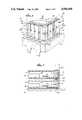
- FIG. 1illustrates the corners of two stacked LCCs according to an embodiment of the present invention.
- FIG. 2is an enlarged cross-sectional view of a portion of the stacked LCCs of the FIG. 1 embodiment, taken along line 2--2.
- FIG. 3is a partially cross-sectional top view of the LCC 100 of FIG. 1, taken along line 3--3.
- FIG. 4is a partially cross-sectional view of a portion of the LCC 100 of FIG. 1, taken along line 3--3.
- FIG. 5is a partially cross-sectional view of a portion of the LCC 101 of FIG. 1, taken along line 5--5.
- FIG. 6is a simplified perspective view of an alternative embodiment of the present invention.
- FIG. 1is a perspective view of a corner of two stacked leadless chip carriers (LCCs) 100, 101 according to an embodiment of the present invention.
- LCCsstacked leadless chip carriers
- Each of the LCCsis boxed-shaped, having substantially rectangular faces.
- Channels 111(FIG. 3) are formed in the side faces, 102, 104, 106 and 108 of each LCC 100 and 101. As will be explained below, each channel 111 is coated with a conductive film 110, and filled with solder 112.
- FIG. 3is a top partially cross-sectional view of the LCC 100 showing 36 channels 111 around its outer periphery. These channels, 111, are numbered 1-36.
- LCC 101is identical to LCC 100. Each channel 111 extends vertically along the side faces 102, 104, 106 and 108, of the LCCs from the top face to the bottom face thereof.
- a cavity 114(FIG. 2) is provided within each of the LCCs for mounting an IC chip 116, 118, therein.
- conductors 110are formed on the walls of the channels 111 with a coating of an electrically conductive material, preferably a gold metallization layer. As shown in FIGS. 1-2, these conductors 110 overlap the top faces of the LCCs to form conductive pads 120 at the top of each channel 111. Similarly, the conductors 110 also overlap the bottom faces of the LCCs to form a conductive pad 122 at the bottom of each channel 111.
- a plurality of "wiring pads” 124are positioned within the cavity 114 of each LCC between the central chip area 113 and the external walls of the LCCs. These wiring pads 124 are electrically connected or “wired” to respective conductors 110 along the exterior surface of the LCCs by means of electrical leads 126.
- the wiring pads 124are numbered 1-36 to refer to the conductor 110 in the numbered channel with which a electrical connection is made. For example, the conductor 110 associated with channel 33 in the upper right-hand corner of FIG. 3 is shown electrically connected to the wiring pad 33 via lead 126. Such leads 126 are integrated into the walls of the LCC 100.
- FIG. 3Also shown in FIG. 3 are several "connecting pads” 128, each of which is labeled "A".
- the several connecting pads 128are electrically connected to each other by any suitable means, such as an electrically conductive bus 130.
- the wiring pad numbered 27is electrically connected with one of the connecting pads, A, via a wire 132.
- the wiring pad 27can provide an enable signal from the conductor of channel 27 to the IC 116, as will be described in greater detail below.
- the LCC 100 described aboveis shown stacked on top of a similar LCC 101.
- the channels 111 of the LCC 100align with respective channels of LCC 101 and the conductive pads 122 located at the bottom of each channel 111 of LCC 100 align with conductive pads 120 located at the top of each channel of LCC 101.
- the aligned conductive padsmay touch, and thus create electrical contacts between the stacked LCCs.
- a spacer 136is provided near each corner of each LCC to maintain a small gap (preferrably, but not necessarily, about 0.010 inch) between the surfaces of the adjacent conductive pads, 120 and 122.
- the spacers 136can be formed by any suitable means, such as screen printing a drop of epoxy on each of the bottom corners of LCC 100 or the top corners of LCC 101, or both.
- Alternative means for spacing the conductive pads of the LCCs, 100 and 101are also within the scope of the present invention. The relevance of the gap between the conductive pads of adjacent LCCs will be discussed below.
- the stackis then dipped into molten solder.
- each side of the LCC stackis sequentially dipped into a vat of molten solder (not shown).
- the molten solderadheres to the metallic conductors (e.g., gold) 110 lining the channels 111, thereby filling the channels 111 with solder 112.
- the solderalso coats the pads 120 and 122.
- the bodies of the LCCsare made of ceramic, and solder will not adhere to the ceramic. Thus, only the channels 111 and conductive pads 120, 122 get coated with solder. Suitable means for applying solder to the stack structure, other than dipping, are also within the scope of the present invention.
- solderis allowed to easily seep between and adhere to the conductive pads, 120 and 122, thereby forming a good electrical and strong mechanical junction between the pads 120, 122.
- a very small gapsuch as 0.010 inch
- the surface tension of the molten solderwill actively draw the solder into the gap between these pads 120, 122. This further ensures a good electrical and strong mechanical connection between stacked LCCs, 100 and 101. Additionally, the gap permits the flow of cleaning solvents between the LCCs to remove flux residue after soldering.
- the stacked LCCsare held together solely by solder, the stacked LCCs can easily be separated for servicing or replacement, without causing damage to the LCCs or ICs carried therein, simply by remelting the solder.
- Identical memory IC chips 116, 118are encapsulated inside each LCC 100, 101 in the stack, and the data, power and ground terminals of each respective IC are connected to the same wiring pads 124, respectively, in each LCC. Nevertheless, the IC encapsulated within each LCC, 100 and 101, in a stack may be selectively enabled while the remainder of the ICs in the stack are not enabled. Selective enablement will now be discussed with reference to FIGS. 4-5.
- FIG. 4is a top partially cross-sectional view of a portion of LCC 100
- FIG. 5is a top partially cross-sectional view of a similar portion of LCC 101.
- FIGS. 4 and 5are identical conventional IC memory chips, 116 and 118, and several IC terminals, 140, 140', 144 and 144' on each of those chips.
- the IC terminal 140 of IC 116is the "enable terminal" of that IC.
- an appropriate electrical signali.e., an enable signal
- the IC 116is enabled and becomes operable.
- no enable signalis applied to the enable terminal 140
- the IC 116is inoperative.
- the memory of IC chip 116can be accessed or altered only when an enable signal is applied to terminal 140.
- the enable terminal 140is electrically connected with one of the connecting pads 128, labeled "A", by a suitable conductive lead 146.
- the "A" connecting pad 128is electrically connected to wiring pad 27 by wire 148.
- the IC 116will be enabled.
- the channel associated with wiring pad 27is called the enable channel for IC 116.
- the IC terminal 144 of IC 116is connected to the conductor 110 of channel 19 through the wiring pad 19 and leads 150 and 126. Depending upon the design of the IC 116, the terminal 144 may be a data input/ouput terminal, a power input terminal or a ground terminal.
- the other IC pads (not shown) of IC 116are similarly connected with the conductors of other channels.
- a similar arrangementis provided for selectively enabling the IC 118 contained in LCC 101.
- Enable terminal 140' of IC 118is electrically connected to an "A" connecting pad 128, much like the enable terminal 140 of IC 116.
- the wiring pad 124 numbered 25is electrically connected to an "A" connecting pad 128.
- an appropriate signal applied to the conductor 110 of channel 25(not 27) is conducted to the enable terminal 140' of IC 118 through the wiring pad 25 and connecting pad A.
- selective enablement of IC 118is accomplished by providing an enable signal on the channel associated with the conductive pad 25.
- Terminal 144' of IC 118is connected to the conductor 110 of channel 19 through wiring pad 19 and leads 126 and 150. In this manner, the IC terminal 144' of IC 118 is connected in parallel with the IC terminal 144 of IC 116.
- data signalsmay be selectively transmitted to and from stacked ICs 116 or 118 by applying such signals to the conductors of channel 19, while simultaneously applying an enable signal to either (but not both) the enable channel of IC 116 or the enable channel of IC 118.
- Other IC terminals (not shown) of IC 118may be similarly connected with the conductors 110 of other channels, as needed.
- each of the data, ground and power terminals of one ICis connected in parallel with respective data, ground and power terminals of all other ICs in the stack.
- the enable input for each ICis connected to the conductor of a different channel than the enable input for every other IC in the stack. In this manner, data can be transmitted to and from any selected IC through the parallel connected data input/output signal terminals, while selective enablement of a particular IC is effected by providing an enable signal on the channel uniquely connected to the enable input terminal of the selected IC.
- the stackcan be further soldered to a single substrate 152 having a dual-in-line lead outline, as illustrated in FIG. 1.
- the stacked LCCs 158may be soldered between two single in-line lead connectors 154.
- Logic chips 156are shown in FIG. 6 on the exterior surfaces of the single in-line lead connectors 154. These chips 156 are used to direct the chip enable signals along the conductor of the appropriate channel for enablement of the selected IC. Similar logic chips (not shown) would also be utilized in connection with the dual-in-line-leaded substrate 152 of FIG. 1. Such logic chips are typically disposed on the bottom side of substrate 152.
- Other substrate and connector lead configurationsare, of course, also within the scope of the present invention.
- FIG. 1illustrates only 2 stacked LCCs, the invention is not so limited.
- the stackmay be formed from as many LCCs as is desired.
- the memory circuit ICs in each stack of LCCsneed not necessarily by identical. In this situation, certain ICs would be connected to more or less data channels than other IC's in the stack.
Landscapes
- Engineering & Computer Science (AREA)
- Microelectronics & Electronic Packaging (AREA)
- Power Engineering (AREA)
- Physics & Mathematics (AREA)
- Condensed Matter Physics & Semiconductors (AREA)
- General Physics & Mathematics (AREA)
- Computer Hardware Design (AREA)
- Structures For Mounting Electric Components On Printed Circuit Boards (AREA)
Abstract
Description
Claims (25)
Priority Applications (1)
| Application Number | Priority Date | Filing Date | Title |
|---|---|---|---|
| US07/267,223US4956694A (en) | 1988-11-04 | 1988-11-04 | Integrated circuit chip stacking |
Applications Claiming Priority (1)
| Application Number | Priority Date | Filing Date | Title |
|---|---|---|---|
| US07/267,223US4956694A (en) | 1988-11-04 | 1988-11-04 | Integrated circuit chip stacking |
Publications (1)
| Publication Number | Publication Date |
|---|---|
| US4956694Atrue US4956694A (en) | 1990-09-11 |
Family
ID=23017855
Family Applications (1)
| Application Number | Title | Priority Date | Filing Date |
|---|---|---|---|
| US07/267,223Expired - LifetimeUS4956694A (en) | 1988-11-04 | 1988-11-04 | Integrated circuit chip stacking |
Country Status (1)
| Country | Link |
|---|---|
| US (1) | US4956694A (en) |
Cited By (217)
| Publication number | Priority date | Publication date | Assignee | Title |
|---|---|---|---|---|
| US5043794A (en)* | 1990-09-24 | 1991-08-27 | At&T Bell Laboratories | Integrated circuit package and compact assemblies thereof |
| US5099309A (en)* | 1990-04-30 | 1992-03-24 | International Business Machines Corporation | Three-dimensional memory card structure with internal direct chip attachment |
| US5113316A (en)* | 1989-11-07 | 1992-05-12 | Marelli Autronica Spa | System for the assembly and connection of electronic circuit boards, particularly for use in motor vehicles |
| JPH04267361A (en)* | 1991-02-22 | 1992-09-22 | Nec Corp | Leadless chip carrier |
| US5165067A (en)* | 1989-12-01 | 1992-11-17 | Inmos Limited | Semiconductor chip packages |
| US5227338A (en)* | 1990-04-30 | 1993-07-13 | International Business Machines Corporation | Three-dimensional memory card structure with internal direct chip attachment |
| US5247423A (en)* | 1992-05-26 | 1993-09-21 | Motorola, Inc. | Stacking three dimensional leadless multi-chip module and method for making the same |
| WO1993019485A1 (en)* | 1992-03-16 | 1993-09-30 | Dense-Pac Microsystems, Inc. | Ic chip package and method of making same |
| US5266833A (en)* | 1992-03-30 | 1993-11-30 | Capps David F | Integrated circuit bus structure |
| US5281852A (en)* | 1991-12-10 | 1994-01-25 | Normington Peter J C | Semiconductor device including stacked die |
| US5343366A (en)* | 1992-06-24 | 1994-08-30 | International Business Machines Corporation | Packages for stacked integrated circuit chip cubes |
| US5367766A (en)* | 1990-08-01 | 1994-11-29 | Staktek Corporation | Ultra high density integrated circuit packages method |
| US5373189A (en)* | 1992-08-13 | 1994-12-13 | Commissariate A L'energie Atomique | Three-dimensional multichip module |
| US5377077A (en)* | 1990-08-01 | 1994-12-27 | Staktek Corporation | Ultra high density integrated circuit packages method and apparatus |
| US5384484A (en)* | 1992-03-10 | 1995-01-24 | Frama Ag | Electronic read-only memory module |
| US5394010A (en)* | 1991-03-13 | 1995-02-28 | Kabushiki Kaisha Toshiba | Semiconductor assembly having laminated semiconductor devices |
| US5397916A (en)* | 1991-12-10 | 1995-03-14 | Normington; Peter J. C. | Semiconductor device including stacked die |
| US5408129A (en)* | 1990-04-18 | 1995-04-18 | Rambus, Inc. | Integrated circuit I/O using a high performance bus interface |
| US5420751A (en)* | 1990-08-01 | 1995-05-30 | Staktek Corporation | Ultra high density modular integrated circuit package |
| US5432999A (en)* | 1992-08-20 | 1995-07-18 | Capps; David F. | Integrated circuit lamination process |
| US5434745A (en)* | 1994-07-26 | 1995-07-18 | White Microelectronics Div. Of Bowmar Instrument Corp. | Stacked silicon die carrier assembly |
| US5446620A (en)* | 1990-08-01 | 1995-08-29 | Staktek Corporation | Ultra high density integrated circuit packages |
| US5455740A (en)* | 1994-03-07 | 1995-10-03 | Staktek Corporation | Bus communication system for stacked high density integrated circuit packages |
| US5475920A (en)* | 1990-08-01 | 1995-12-19 | Burns; Carmen D. | Method of assembling ultra high density integrated circuit packages |
| US5493096A (en)* | 1994-05-10 | 1996-02-20 | Grumman Aerospace Corporation | Thin substrate micro-via interconnect |
| US5495397A (en)* | 1993-04-27 | 1996-02-27 | International Business Machines Corporation | Three dimensional package and architecture for high performance computer |
| US5499160A (en)* | 1990-08-01 | 1996-03-12 | Staktek Corporation | High density integrated circuit module with snap-on rail assemblies |
| US5508565A (en)* | 1992-12-18 | 1996-04-16 | Fujitsu Limited | Semiconductor device having a plurality of chips having identical circuit arrangement sealed in package |
| US5541812A (en)* | 1995-05-22 | 1996-07-30 | Burns; Carmen D. | Bus communication system for stacked high density integrated circuit packages having an intermediate lead frame |
| US5588205A (en)* | 1995-01-24 | 1996-12-31 | Staktek Corporation | Method of manufacturing a high density integrated circuit module having complex electrical interconnect rails |
| US5592364A (en)* | 1995-01-24 | 1997-01-07 | Staktek Corporation | High density integrated circuit module with complex electrical interconnect rails |
| US5600101A (en)* | 1994-07-21 | 1997-02-04 | Murata Manufacturing Co., Ltd. | Multilayer electronic component and method of manufacturing the same |
| US5602420A (en)* | 1992-09-07 | 1997-02-11 | Hitachi, Ltd. | Stacked high mounting density semiconductor devices |
| US5612570A (en)* | 1995-04-13 | 1997-03-18 | Dense-Pac Microsystems, Inc. | Chip stack and method of making same |
| US5621193A (en)* | 1995-05-23 | 1997-04-15 | Northrop Grumman Corporation | Ceramic edge connect process |
| US5648684A (en)* | 1995-07-26 | 1997-07-15 | International Business Machines Corporation | Endcap chip with conductive, monolithic L-connect for multichip stack |
| US5648683A (en)* | 1993-08-13 | 1997-07-15 | Kabushiki Kaisha Toshiba | Semiconductor device in which a first resin-encapsulated package is mounted on a second resin-encapsulated package |
| US5657206A (en)* | 1994-06-23 | 1997-08-12 | Cubic Memory, Inc. | Conductive epoxy flip-chip package and method |
| US5656856A (en)* | 1994-06-09 | 1997-08-12 | Samsung Electronics Co., Ltd. | Reduced noise semiconductor package stack |
| US5661087A (en)* | 1994-06-23 | 1997-08-26 | Cubic Memory, Inc. | Vertical interconnect process for silicon segments |
| US5698895A (en)* | 1994-06-23 | 1997-12-16 | Cubic Memory, Inc. | Silicon segment programming method and apparatus |
| US5706172A (en)* | 1995-08-16 | 1998-01-06 | Samsung Electronics Co., Ltd. | Stacked semiconductor package having supporting bars and a socket therefor |
| US5723901A (en)* | 1994-12-13 | 1998-03-03 | Kabushiki Kaisha Toshiba | Stacked semiconductor device having peripheral through holes |
| US5778522A (en)* | 1996-05-20 | 1998-07-14 | Staktek Corporation | Method of manufacturing a high density integrated circuit module with complex electrical interconnect rails having electrical interconnect strain relief |
| US5783464A (en)* | 1992-06-26 | 1998-07-21 | Staktek Corporation | Method of forming a hermetically sealed circuit lead-on package |
| US5847448A (en)* | 1990-12-11 | 1998-12-08 | Thomson-Csf | Method and device for interconnecting integrated circuits in three dimensions |
| US5869353A (en)* | 1997-11-17 | 1999-02-09 | Dense-Pac Microsystems, Inc. | Modular panel stacking process |
| US5891761A (en)* | 1994-06-23 | 1999-04-06 | Cubic Memory, Inc. | Method for forming vertical interconnect process for silicon segments with thermally conductive epoxy preform |
| US5956234A (en)* | 1998-01-20 | 1999-09-21 | Integrated Device Technology, Inc. | Method and structure for a surface mountable rigid-flex printed circuit board |
| WO1999022570A3 (en)* | 1997-11-03 | 1999-10-07 | Amtech R Int Inc | Three-dimensional electronic module |
| US5978227A (en)* | 1993-03-29 | 1999-11-02 | Staktek Corporation | Integrated circuit packages having an externally mounted lead frame having bifurcated distal lead ends |
| US6025642A (en)* | 1995-08-17 | 2000-02-15 | Staktek Corporation | Ultra high density integrated circuit packages |
| US6072233A (en)* | 1998-05-04 | 2000-06-06 | Micron Technology, Inc. | Stackable ball grid array package |
| US6080596A (en)* | 1994-06-23 | 2000-06-27 | Cubic Memory Inc. | Method for forming vertical interconnect process for silicon segments with dielectric isolation |
| US6121576A (en)* | 1998-09-02 | 2000-09-19 | Micron Technology, Inc. | Method and process of contact to a heat softened solder ball array |
| US6124633A (en)* | 1994-06-23 | 2000-09-26 | Cubic Memory | Vertical interconnect process for silicon segments with thermally conductive epoxy preform |
| USRE36916E (en)* | 1995-03-21 | 2000-10-17 | Simple Technology Incorporated | Apparatus for stacking semiconductor chips |
| US6180881B1 (en) | 1998-05-05 | 2001-01-30 | Harlan Ruben Isaak | Chip stack and method of making same |
| US6190425B1 (en) | 1998-11-03 | 2001-02-20 | Zomaya Group, Inc. | Memory bar and related circuits and methods |
| US6222737B1 (en) | 1999-04-23 | 2001-04-24 | Dense-Pac Microsystems, Inc. | Universal package and method of forming the same |
| US6242285B1 (en) | 1998-07-23 | 2001-06-05 | Kyung Suk Kang | Stacked package of semiconductor package units via direct connection between leads and stacking method therefor |
| US6255726B1 (en) | 1994-06-23 | 2001-07-03 | Cubic Memory, Inc. | Vertical interconnect process for silicon segments with dielectric isolation |
| US6262895B1 (en) | 2000-01-13 | 2001-07-17 | John A. Forthun | Stackable chip package with flex carrier |
| US6278616B1 (en)* | 1998-07-07 | 2001-08-21 | Texas Instruments Incorporated | Modifying memory device organization in high density packages |
| US6295220B1 (en) | 1998-11-03 | 2001-09-25 | Zomaya Group, Inc. | Memory bar and related circuits and methods |
| US6313998B1 (en) | 1999-04-02 | 2001-11-06 | Legacy Electronics, Inc. | Circuit board assembly having a three dimensional array of integrated circuit packages |
| US6323060B1 (en) | 1999-05-05 | 2001-11-27 | Dense-Pac Microsystems, Inc. | Stackable flex circuit IC package and method of making same |
| US6351029B1 (en) | 1999-05-05 | 2002-02-26 | Harlan R. Isaak | Stackable flex circuit chip package and method of making same |
| US6372527B1 (en) | 1990-09-24 | 2002-04-16 | Tessera, Inc. | Methods of making semiconductor chip assemblies |
| US6404043B1 (en) | 2000-06-21 | 2002-06-11 | Dense-Pac Microsystems, Inc. | Panel stacking of BGA devices to form three-dimensional modules |
| US6417695B1 (en) | 2001-03-15 | 2002-07-09 | Micron Technology, Inc. | Antifuse reroute of dies |
| US6462408B1 (en) | 2001-03-27 | 2002-10-08 | Staktek Group, L.P. | Contact member stacking system and method |
| US6486528B1 (en) | 1994-06-23 | 2002-11-26 | Vertical Circuits, Inc. | Silicon segment programming apparatus and three terminal fuse configuration |
| US20030002267A1 (en)* | 2001-06-15 | 2003-01-02 | Mantz Frank E. | I/O interface structure |
| US20030006684A1 (en)* | 2001-03-27 | 2003-01-09 | Shinichi Kawate | Catalyst used to form carbon fiber, method of making the same and electron emitting device, electron source, image forming apparatus, secondary battery and body for storing hydrogen |
| KR100368968B1 (en)* | 2000-06-30 | 2003-01-24 | 주식회사 하이닉스반도체 | Stack type package |
| US20030025211A1 (en)* | 2001-07-24 | 2003-02-06 | Ted Bruce | Chip stack with differing chip package types |
| US6518659B1 (en)* | 2000-05-08 | 2003-02-11 | Amkor Technology, Inc. | Stackable package having a cavity and a lid for an electronic device |
| US20030051911A1 (en)* | 2001-09-20 | 2003-03-20 | Roeters Glen E. | Post in ring interconnect using 3-D stacking |
| US20030081392A1 (en)* | 2001-10-26 | 2003-05-01 | Staktek Group, L.P. | Integrated circuit stacking system and method |
| EP0713609B1 (en)* | 1993-08-13 | 2003-05-07 | Irvine Sensors Corporation | Stack of ic chips as substitute for single ic chip |
| US6573461B2 (en) | 2001-09-20 | 2003-06-03 | Dpac Technologies Corp | Retaining ring interconnect used for 3-D stacking |
| US6572387B2 (en) | 1999-09-24 | 2003-06-03 | Staktek Group, L.P. | Flexible circuit connector for stacked chip module |
| US6576992B1 (en) | 2001-10-26 | 2003-06-10 | Staktek Group L.P. | Chip scale stacking system and method |
| US20030107118A1 (en)* | 2001-10-09 | 2003-06-12 | Tessera, Inc. | Stacked packages |
| US20030131472A1 (en)* | 2002-01-15 | 2003-07-17 | Mitac International Corp. | Method of fabricating a multi-layer circuit board assembly |
| US6608763B1 (en) | 2000-09-15 | 2003-08-19 | Staktek Group L.P. | Stacking system and method |
| US6609915B2 (en)* | 2001-11-30 | 2003-08-26 | Fci Americas Technology | Interconnect for electrically connecting a multichip module to a circuit substrate and processes for making and using same |
| US20030192171A1 (en)* | 2002-01-16 | 2003-10-16 | Fey Kate E. | Space-saving packaging of electronic circuits |
| US6660561B2 (en) | 2000-06-15 | 2003-12-09 | Dpac Technologies Corp. | Method of assembling a stackable integrated circuit chip |
| US6667544B1 (en)* | 2000-06-30 | 2003-12-23 | Amkor Technology, Inc. | Stackable package having clips for fastening package and tool for opening clips |
| US20040031972A1 (en)* | 2001-10-09 | 2004-02-19 | Tessera, Inc. | Stacked packages |
| US20040052060A1 (en)* | 2001-10-26 | 2004-03-18 | Staktek Group, L.P. | Low profile chip scale stacking system and method |
| US6709964B2 (en) | 1999-07-21 | 2004-03-23 | Samsung Electronics Co., Ltd. | Semiconductor device and manufacturing method using a stress-relieving film attached to solder joints |
| GB2364440B (en)* | 1999-05-07 | 2004-05-26 | Seagate Technology Llc | Surface mount ic stacking method and device |
| US20040099938A1 (en)* | 2002-09-11 | 2004-05-27 | Tessera, Inc. | Assemblies having stacked semiconductor chips and methods of making same |
| US20040104470A1 (en)* | 2002-08-16 | 2004-06-03 | Tessera, Inc. | Microelectronic packages with self-aligning features |
| GB2396056A (en)* | 1999-05-07 | 2004-06-09 | Seagate Technology Llc | Surface mount ic stacking method and device |
| US20040108584A1 (en)* | 2002-12-05 | 2004-06-10 | Roeters Glen E. | Thin scale outline package |
| US20040124523A1 (en)* | 2002-06-18 | 2004-07-01 | Poo Chia Yong | Semiconductor devices including peripherally located bond pads, intermediates thereof, assemblies, and packages including the semiconductor devices, and support elements for the semiconductor devices |
| US20040157410A1 (en)* | 2003-01-16 | 2004-08-12 | Seiko Epson Corporation | Semiconductor device, semiconductor module, electronic equipment, method for manufacturing semiconductor device, and method for manufacturing semiconductor module |
| US20040178496A1 (en)* | 2001-10-26 | 2004-09-16 | Staktek Grop, L.P. | Memory expansion and chip scale stacking system and method |
| US20040183183A1 (en)* | 2001-10-26 | 2004-09-23 | Staktek Group, L.P. | Integrated circuit stacking system and method |
| US20040191442A1 (en)* | 2003-03-27 | 2004-09-30 | Florencia Lim | Surface modification of expanded ultra high molecular weight polyethylene (eUHMWPE) for improved bondability |
| US20040207990A1 (en)* | 2003-04-21 | 2004-10-21 | Rose Andrew C. | Stair-step signal routing |
| US20040217461A1 (en)* | 2002-08-05 | 2004-11-04 | Tessera, Inc. | Microelectronic adaptors, assemblies and methods |
| US6885106B1 (en) | 2001-01-11 | 2005-04-26 | Tessera, Inc. | Stacked microelectronic assemblies and methods of making same |
| US6897090B2 (en) | 1994-12-29 | 2005-05-24 | Tessera, Inc. | Method of making a compliant integrated circuit package |
| EP1168441A3 (en)* | 2000-06-23 | 2005-06-15 | Shinko Electric Industries Co. Ltd. | Multi-layer wiring substrate and semiconductor device using the multi-layer wiring substrate |
| US6919626B2 (en) | 1992-12-11 | 2005-07-19 | Staktek Group L.P. | High density integrated circuit module |
| US20050194672A1 (en)* | 2003-11-04 | 2005-09-08 | Tessera, Inc. | Stacked packages and systems incorporating the same |
| US20050224952A1 (en)* | 2004-04-13 | 2005-10-13 | Al Vindasius | Three dimensional six surface conformal die coating |
| US6977431B1 (en) | 2003-11-05 | 2005-12-20 | Amkor Technology, Inc. | Stackable semiconductor package and manufacturing method thereof |
| US20060006521A1 (en)* | 2003-09-30 | 2006-01-12 | Boon Suan J | Semiconductor device assemblies and packages with edge contacts and sacrificial substrates and other intermediate structures used or formed in fabricating the assemblies or packages |
| EP1617714A1 (en)* | 2004-07-16 | 2006-01-18 | STMicroelectronics S.A. | Electronic circuit assembly, device comprising such assembly and method for fabricating such device |
| US20060022310A1 (en)* | 2004-07-28 | 2006-02-02 | Endicott Interconnect Technologies, Inc. | Electrical assembly with internal memory circuitized substrate having electronic components positioned thereon, method of making same, and information handling system utilizing same |
| US20060022303A1 (en)* | 2004-07-28 | 2006-02-02 | Endicott Interconnect Technologies, Inc. | Circuitized substrate with internal organic memory device, method of making same, electrical assembly utilizing same, and information handling system utilizing same |
| US7012811B1 (en)* | 2000-05-10 | 2006-03-14 | Micron Technology, Inc. | Method of tuning a multi-path circuit |
| US7033861B1 (en) | 2005-05-18 | 2006-04-25 | Staktek Group L.P. | Stacked module systems and method |
| US7053478B2 (en) | 2001-10-26 | 2006-05-30 | Staktek Group L.P. | Pitch change and chip scale stacking system |
| US7081373B2 (en) | 2001-12-14 | 2006-07-25 | Staktek Group, L.P. | CSP chip stack with flex circuit |
| US20060186514A1 (en)* | 2005-02-22 | 2006-08-24 | Stats Chippac Ltd. | Package stacking lead frame system |
| US7098078B2 (en) | 1990-09-24 | 2006-08-29 | Tessera, Inc. | Microelectronic component and assembly having leads with offset portions |
| US7180167B2 (en) | 2001-10-26 | 2007-02-20 | Staktek Group L. P. | Low profile stacking system and method |
| US7202555B2 (en) | 2001-10-26 | 2007-04-10 | Staktek Group L.P. | Pitch change and chip scale stacking system and method |
| US7215018B2 (en) | 2004-04-13 | 2007-05-08 | Vertical Circuits, Inc. | Stacked die BGA or LGA component assembly |
| US7226809B2 (en)* | 2002-06-18 | 2007-06-05 | Micron Technology, Inc. | Semiconductor devices and semiconductor device components with peripherally located, castellated contacts, assemblies and packages including such semiconductor devices or packages and associated methods |
| US7245021B2 (en) | 2004-04-13 | 2007-07-17 | Vertical Circuits, Inc. | Micropede stacked die component assembly |
| US20070176297A1 (en)* | 2006-01-31 | 2007-08-02 | Tessera, Inc. | Reworkable stacked chip assembly |
| US7289327B2 (en) | 2006-02-27 | 2007-10-30 | Stakick Group L.P. | Active cooling methods and apparatus for modules |
| US7304382B2 (en) | 2006-01-11 | 2007-12-04 | Staktek Group L.P. | Managed memory component |
| US20070278642A1 (en)* | 2006-05-31 | 2007-12-06 | Sony Corporation | Semiconductor device |
| US7310458B2 (en) | 2001-10-26 | 2007-12-18 | Staktek Group L.P. | Stacked module systems and methods |
| US7309914B2 (en) | 2005-01-20 | 2007-12-18 | Staktek Group L.P. | Inverted CSP stacking system and method |
| US7324352B2 (en) | 2004-09-03 | 2008-01-29 | Staktek Group L.P. | High capacity thin module system and method |
| US20080023853A1 (en)* | 1995-12-19 | 2008-01-31 | Micron Technology, Inc. | Flip chip adaptor package for bare die |
| US20080042250A1 (en)* | 2006-08-18 | 2008-02-21 | Tessera, Inc. | Stacked microelectronic assemblies and methods therefor |
| US20080042274A1 (en)* | 2002-09-06 | 2008-02-21 | Tessera, Inc. | Components, methods and assemblies for stacked packages |
| US7335995B2 (en) | 2001-10-09 | 2008-02-26 | Tessera, Inc. | Microelectronic assembly having array including passive elements and interconnects |
| US7371609B2 (en) | 2001-10-26 | 2008-05-13 | Staktek Group L.P. | Stacked module systems and methods |
| US7417310B2 (en) | 2006-11-02 | 2008-08-26 | Entorian Technologies, Lp | Circuit module having force resistant construction |
| US7423885B2 (en) | 2004-09-03 | 2008-09-09 | Entorian Technologies, Lp | Die module system |
| US20080244902A1 (en)* | 2007-04-09 | 2008-10-09 | Endicott Interconnect Technologies, Inc. | Circuitized substrate with internal stacked semiconductor chips, method of making same, electrical assembly utilizing same and information handling system utilizing same |
| US7443023B2 (en) | 2004-09-03 | 2008-10-28 | Entorian Technologies, Lp | High capacity thin module system |
| US7446410B2 (en) | 2004-09-03 | 2008-11-04 | Entorian Technologies, Lp | Circuit module with thermal casing systems |
| US7468553B2 (en) | 2006-10-20 | 2008-12-23 | Entorian Technologies, Lp | Stackable micropackages and stacked modules |
| US7468893B2 (en) | 2004-09-03 | 2008-12-23 | Entorian Technologies, Lp | Thin module system and method |
| US20090008795A1 (en)* | 2007-07-02 | 2009-01-08 | Tessera, Inc. | Stackable microelectronic device carriers, stacked device carriers and methods of making the same |
| US7480152B2 (en) | 2004-09-03 | 2009-01-20 | Entorian Technologies, Lp | Thin module system and method |
| US7485951B2 (en) | 2001-10-26 | 2009-02-03 | Entorian Technologies, Lp | Modularized die stacking system and method |
| US7508069B2 (en) | 2006-01-11 | 2009-03-24 | Entorian Technologies, Lp | Managed memory component |
| US7508058B2 (en) | 2006-01-11 | 2009-03-24 | Entorian Technologies, Lp | Stacked integrated circuit module |
| US7511969B2 (en) | 2006-02-02 | 2009-03-31 | Entorian Technologies, Lp | Composite core circuit module system and method |
| US7511968B2 (en) | 2004-09-03 | 2009-03-31 | Entorian Technologies, Lp | Buffered thin module system and method |
| US7522421B2 (en) | 2004-09-03 | 2009-04-21 | Entorian Technologies, Lp | Split core circuit module |
| US7542297B2 (en) | 2004-09-03 | 2009-06-02 | Entorian Technologies, Lp | Optimized mounting area circuit module system and method |
| US7542304B2 (en) | 2003-09-15 | 2009-06-02 | Entorian Technologies, Lp | Memory expansion and integrated circuit stacking system and method |
| US20090175014A1 (en)* | 2008-01-03 | 2009-07-09 | Jian-Hong Zeng | Assembled circuit and electronic component |
| US7576995B2 (en) | 2005-11-04 | 2009-08-18 | Entorian Technologies, Lp | Flex circuit apparatus and method for adding capacitance while conserving circuit board surface area |
| US7579687B2 (en) | 2004-09-03 | 2009-08-25 | Entorian Technologies, Lp | Circuit module turbulence enhancement systems and methods |
| US20090251873A1 (en)* | 2008-04-02 | 2009-10-08 | Sun-Wen Cyrus Cheng | Surface Mount Power Module Dual Footprint |
| US7606049B2 (en) | 2004-09-03 | 2009-10-20 | Entorian Technologies, Lp | Module thermal management system and method |
| US7606040B2 (en) | 2004-09-03 | 2009-10-20 | Entorian Technologies, Lp | Memory module system and method |
| US7605454B2 (en) | 2006-01-11 | 2009-10-20 | Entorian Technologies, Lp | Memory card and method for devising |
| US7606050B2 (en) | 2004-09-03 | 2009-10-20 | Entorian Technologies, Lp | Compact module system and method |
| US7608920B2 (en) | 2006-01-11 | 2009-10-27 | Entorian Technologies, Lp | Memory card and method for devising |
| US7616452B2 (en) | 2004-09-03 | 2009-11-10 | Entorian Technologies, Lp | Flex circuit constructions for high capacity circuit module systems and methods |
| US7656678B2 (en) | 2001-10-26 | 2010-02-02 | Entorian Technologies, Lp | Stacked module systems |
| US7719098B2 (en) | 2001-10-26 | 2010-05-18 | Entorian Technologies Lp | Stacked modules and method |
| US7760513B2 (en) | 2004-09-03 | 2010-07-20 | Entorian Technologies Lp | Modified core for circuit module system and method |
| US20100284161A1 (en)* | 2008-01-22 | 2010-11-11 | Olympus Corporation | Stacked mounting structure |
| US20110013373A1 (en)* | 2009-07-14 | 2011-01-20 | Apple Inc. | Systems and methods for providing vias through a modular component |
| US7990746B2 (en) | 2005-06-24 | 2011-08-02 | Google Inc. | Method and circuit for configuring memory core integrated circuit dies with memory interface integrated circuit dies |
| US8019589B2 (en) | 2006-07-31 | 2011-09-13 | Google Inc. | Memory apparatus operable to perform a power-saving operation |
| US8055833B2 (en) | 2006-10-05 | 2011-11-08 | Google Inc. | System and method for increasing capacity, performance, and flexibility of flash storage |
| US8060774B2 (en) | 2005-06-24 | 2011-11-15 | Google Inc. | Memory systems and memory modules |
| US8081474B1 (en) | 2007-12-18 | 2011-12-20 | Google Inc. | Embossed heat spreader |
| US8080874B1 (en) | 2007-09-14 | 2011-12-20 | Google Inc. | Providing additional space between an integrated circuit and a circuit board for positioning a component therebetween |
| US8089795B2 (en) | 2006-02-09 | 2012-01-03 | Google Inc. | Memory module with memory stack and interface with enhanced capabilities |
| US8090897B2 (en) | 2006-07-31 | 2012-01-03 | Google Inc. | System and method for simulating an aspect of a memory circuit |
| USRE43112E1 (en) | 1998-05-04 | 2012-01-17 | Round Rock Research, Llc | Stackable ball grid array package |
| US8111566B1 (en) | 2007-11-16 | 2012-02-07 | Google, Inc. | Optimal channel design for memory devices for providing a high-speed memory interface |
| US8122207B2 (en) | 2006-07-31 | 2012-02-21 | Google Inc. | Apparatus and method for power management of memory circuits by a system or component thereof |
| US8130560B1 (en) | 2006-11-13 | 2012-03-06 | Google Inc. | Multi-rank partial width memory modules |
| US8154935B2 (en) | 2006-07-31 | 2012-04-10 | Google Inc. | Delaying a signal communicated from a system to at least one of a plurality of memory circuits |
| US8169233B2 (en) | 2009-06-09 | 2012-05-01 | Google Inc. | Programming of DIMM termination resistance values |
| US8181048B2 (en) | 2006-07-31 | 2012-05-15 | Google Inc. | Performing power management operations |
| US8209479B2 (en) | 2007-07-18 | 2012-06-26 | Google Inc. | Memory circuit system and method |
| US8213205B2 (en) | 2005-09-02 | 2012-07-03 | Google Inc. | Memory system including multiple memory stacks |
| US20120187577A1 (en)* | 2007-06-19 | 2012-07-26 | International Business Machines Corporation | Direct Edge Connection for Multi-Chip Integrated Circuits |
| US8244971B2 (en) | 2006-07-31 | 2012-08-14 | Google Inc. | Memory circuit system and method |
| US8280714B2 (en) | 2006-07-31 | 2012-10-02 | Google Inc. | Memory circuit simulation system and method with refresh capabilities |
| USD668659S1 (en)* | 2011-11-15 | 2012-10-09 | Connectblue Ab | Module |
| USD668658S1 (en)* | 2011-11-15 | 2012-10-09 | Connectblue Ab | Module |
| US8327104B2 (en) | 2006-07-31 | 2012-12-04 | Google Inc. | Adjusting the timing of signals associated with a memory system |
| US8335894B1 (en) | 2008-07-25 | 2012-12-18 | Google Inc. | Configurable memory system with interface circuit |
| US8386722B1 (en) | 2008-06-23 | 2013-02-26 | Google Inc. | Stacked DIMM memory interface |
| US8397013B1 (en) | 2006-10-05 | 2013-03-12 | Google Inc. | Hybrid memory module |
| USD680119S1 (en)* | 2011-11-15 | 2013-04-16 | Connectblue Ab | Module |
| USD680545S1 (en)* | 2011-11-15 | 2013-04-23 | Connectblue Ab | Module |
| US8438328B2 (en) | 2008-02-21 | 2013-05-07 | Google Inc. | Emulation of abstracted DIMMs using abstracted DRAMs |
| USD689053S1 (en)* | 2011-11-15 | 2013-09-03 | Connectblue Ab | Module |
| US8566516B2 (en) | 2006-07-31 | 2013-10-22 | Google Inc. | Refresh management of memory modules |
| USD692896S1 (en)* | 2011-11-15 | 2013-11-05 | Connectblue Ab | Module |
| US8773937B2 (en) | 2005-06-24 | 2014-07-08 | Google Inc. | Memory refresh apparatus and method |
| US8796830B1 (en) | 2006-09-01 | 2014-08-05 | Google Inc. | Stackable low-profile lead frame package |
| US8890327B2 (en) | 2005-12-01 | 2014-11-18 | Tessera, Inc. | Stacked microelectronic packages having at least two stacked microelectronic elements adjacent one another |
| US20150011126A1 (en)* | 2013-07-02 | 2015-01-08 | Pulse Electronics, Inc. | Methods and apparatus for terminating wire wound electronic components to an insert header assembly |
| US8949519B2 (en) | 2005-06-24 | 2015-02-03 | Google Inc. | Simulating a memory circuit |
| USRE45463E1 (en) | 2003-11-12 | 2015-04-14 | Tessera, Inc. | Stacked microelectronic assemblies with central contacts |
| US9171585B2 (en) | 2005-06-24 | 2015-10-27 | Google Inc. | Configurable memory circuit system and method |
| US9507739B2 (en) | 2005-06-24 | 2016-11-29 | Google Inc. | Configurable memory circuit system and method |
| US9542352B2 (en) | 2006-02-09 | 2017-01-10 | Google Inc. | System and method for reducing command scheduling constraints of memory circuits |
| US9601857B2 (en) | 2013-05-23 | 2017-03-21 | Pulse Electronics, Inc. | Methods and apparatus for terminating wire wound electronic devices |
| US9632929B2 (en) | 2006-02-09 | 2017-04-25 | Google Inc. | Translating an address associated with a command communicated between a system and memory circuits |
| US10013371B2 (en) | 2005-06-24 | 2018-07-03 | Google Llc | Configurable memory circuit system and method |
| US20220223558A1 (en)* | 2019-08-27 | 2022-07-14 | Mitsubishi Electric Corporation | Semiconductor device |
Citations (5)
| Publication number | Priority date | Publication date | Assignee | Title |
|---|---|---|---|---|
| US4371912A (en)* | 1980-10-01 | 1983-02-01 | Motorola, Inc. | Method of mounting interrelated components |
| US4638348A (en)* | 1982-08-10 | 1987-01-20 | Brown David F | Semiconductor chip carrier |
| US4761681A (en)* | 1982-09-08 | 1988-08-02 | Texas Instruments Incorporated | Method for fabricating a semiconductor contact and interconnect structure using orientation dependent etching and thermomigration |
| US4841355A (en)* | 1988-02-10 | 1989-06-20 | Amdahl Corporation | Three-dimensional microelectronic package for semiconductor chips |
| US4868712A (en)* | 1987-02-04 | 1989-09-19 | Woodman John K | Three dimensional integrated circuit package |
- 1988
- 1988-11-04USUS07/267,223patent/US4956694A/ennot_activeExpired - Lifetime
Patent Citations (5)
| Publication number | Priority date | Publication date | Assignee | Title |
|---|---|---|---|---|
| US4371912A (en)* | 1980-10-01 | 1983-02-01 | Motorola, Inc. | Method of mounting interrelated components |
| US4638348A (en)* | 1982-08-10 | 1987-01-20 | Brown David F | Semiconductor chip carrier |
| US4761681A (en)* | 1982-09-08 | 1988-08-02 | Texas Instruments Incorporated | Method for fabricating a semiconductor contact and interconnect structure using orientation dependent etching and thermomigration |
| US4868712A (en)* | 1987-02-04 | 1989-09-19 | Woodman John K | Three dimensional integrated circuit package |
| US4841355A (en)* | 1988-02-10 | 1989-06-20 | Amdahl Corporation | Three-dimensional microelectronic package for semiconductor chips |
Non-Patent Citations (4)
| Title |
|---|
| "Megabyte Per Cubic Inch", Defense Science, p. 56, May 1988. |
| "Three-Dimensional Packaging", Defense Science, p. 65, May 1988. |
| Megabyte Per Cubic Inch , Defense Science, p. 56, May 1988.* |
| Three Dimensional Packaging , Defense Science, p. 65, May 1988.* |
Cited By (398)
| Publication number | Priority date | Publication date | Assignee | Title |
|---|---|---|---|---|
| US5113316A (en)* | 1989-11-07 | 1992-05-12 | Marelli Autronica Spa | System for the assembly and connection of electronic circuit boards, particularly for use in motor vehicles |
| US5512783A (en)* | 1989-12-01 | 1996-04-30 | Inmos Limited | Semiconductor chip packages |
| US5165067A (en)* | 1989-12-01 | 1992-11-17 | Inmos Limited | Semiconductor chip packages |
| US5408129A (en)* | 1990-04-18 | 1995-04-18 | Rambus, Inc. | Integrated circuit I/O using a high performance bus interface |
| US5280192A (en)* | 1990-04-30 | 1994-01-18 | International Business Machines Corporation | Three-dimensional memory card structure with internal direct chip attachment |
| US5099309A (en)* | 1990-04-30 | 1992-03-24 | International Business Machines Corporation | Three-dimensional memory card structure with internal direct chip attachment |
| US5227338A (en)* | 1990-04-30 | 1993-07-13 | International Business Machines Corporation | Three-dimensional memory card structure with internal direct chip attachment |
| US5367766A (en)* | 1990-08-01 | 1994-11-29 | Staktek Corporation | Ultra high density integrated circuit packages method |
| US5420751A (en)* | 1990-08-01 | 1995-05-30 | Staktek Corporation | Ultra high density modular integrated circuit package |
| US5475920A (en)* | 1990-08-01 | 1995-12-19 | Burns; Carmen D. | Method of assembling ultra high density integrated circuit packages |
| US6049123A (en)* | 1990-08-01 | 2000-04-11 | Staktek Corporation | Ultra high density integrated circuit packages |
| US5543664A (en)* | 1990-08-01 | 1996-08-06 | Staktek Corporation | Ultra high density integrated circuit package |
| US5550711A (en)* | 1990-08-01 | 1996-08-27 | Staktek Corporation | Ultra high density integrated circuit packages |
| US5561591A (en)* | 1990-08-01 | 1996-10-01 | Staktek Corporation | Multi-signal rail assembly with impedance control for a three-dimensional high density integrated circuit package |
| US5499160A (en)* | 1990-08-01 | 1996-03-12 | Staktek Corporation | High density integrated circuit module with snap-on rail assemblies |
| US5446620A (en)* | 1990-08-01 | 1995-08-29 | Staktek Corporation | Ultra high density integrated circuit packages |
| US5377077A (en)* | 1990-08-01 | 1994-12-27 | Staktek Corporation | Ultra high density integrated circuit packages method and apparatus |
| US6168970B1 (en) | 1990-08-01 | 2001-01-02 | Staktek Group L.P. | Ultra high density integrated circuit packages |
| US5566051A (en)* | 1990-08-01 | 1996-10-15 | Staktek Corporation | Ultra high density integrated circuit packages method and apparatus |
| US7271481B2 (en) | 1990-09-24 | 2007-09-18 | Tessera, Inc. | Microelectronic component and assembly having leads with offset portions |
| US7198969B1 (en) | 1990-09-24 | 2007-04-03 | Tessera, Inc. | Semiconductor chip assemblies, methods of making same and components for same |
| US5043794A (en)* | 1990-09-24 | 1991-08-27 | At&T Bell Laboratories | Integrated circuit package and compact assemblies thereof |
| US7098078B2 (en) | 1990-09-24 | 2006-08-29 | Tessera, Inc. | Microelectronic component and assembly having leads with offset portions |
| US6465893B1 (en) | 1990-09-24 | 2002-10-15 | Tessera, Inc. | Stacked chip assembly |
| US6372527B1 (en) | 1990-09-24 | 2002-04-16 | Tessera, Inc. | Methods of making semiconductor chip assemblies |
| US7291910B2 (en) | 1990-09-24 | 2007-11-06 | Tessera, Inc. | Semiconductor chip assemblies, methods of making same and components for same |
| US5847448A (en)* | 1990-12-11 | 1998-12-08 | Thomson-Csf | Method and device for interconnecting integrated circuits in three dimensions |
| JPH04267361A (en)* | 1991-02-22 | 1992-09-22 | Nec Corp | Leadless chip carrier |
| US5394010A (en)* | 1991-03-13 | 1995-02-28 | Kabushiki Kaisha Toshiba | Semiconductor assembly having laminated semiconductor devices |
| US5397916A (en)* | 1991-12-10 | 1995-03-14 | Normington; Peter J. C. | Semiconductor device including stacked die |
| US5281852A (en)* | 1991-12-10 | 1994-01-25 | Normington Peter J C | Semiconductor device including stacked die |
| US5475260A (en)* | 1992-03-10 | 1995-12-12 | Frama Ag | Electronic read-only module |
| US5384484A (en)* | 1992-03-10 | 1995-01-24 | Frama Ag | Electronic read-only memory module |
| WO1993019485A1 (en)* | 1992-03-16 | 1993-09-30 | Dense-Pac Microsystems, Inc. | Ic chip package and method of making same |
| US5313096A (en)* | 1992-03-16 | 1994-05-17 | Dense-Pac Microsystems, Inc. | IC chip package having chip attached to and wire bonded within an overlying substrate |
| US5266833A (en)* | 1992-03-30 | 1993-11-30 | Capps David F | Integrated circuit bus structure |
| US5247423A (en)* | 1992-05-26 | 1993-09-21 | Motorola, Inc. | Stacking three dimensional leadless multi-chip module and method for making the same |
| EP0862217A3 (en)* | 1992-05-26 | 1999-12-15 | Motorola, Inc. | Semiconductor device and semiconductor multi-chip module |
| EP0571749A1 (en)* | 1992-05-26 | 1993-12-01 | Motorola, Inc. | Stacking semiconductor multi-chip module and method for making the same |
| US5343366A (en)* | 1992-06-24 | 1994-08-30 | International Business Machines Corporation | Packages for stacked integrated circuit chip cubes |
| US5783464A (en)* | 1992-06-26 | 1998-07-21 | Staktek Corporation | Method of forming a hermetically sealed circuit lead-on package |
| US5373189A (en)* | 1992-08-13 | 1994-12-13 | Commissariate A L'energie Atomique | Three-dimensional multichip module |
| US5432999A (en)* | 1992-08-20 | 1995-07-18 | Capps; David F. | Integrated circuit lamination process |
| US5602420A (en)* | 1992-09-07 | 1997-02-11 | Hitachi, Ltd. | Stacked high mounting density semiconductor devices |
| US6919626B2 (en) | 1992-12-11 | 2005-07-19 | Staktek Group L.P. | High density integrated circuit module |
| US5508565A (en)* | 1992-12-18 | 1996-04-16 | Fujitsu Limited | Semiconductor device having a plurality of chips having identical circuit arrangement sealed in package |
| US5978227A (en)* | 1993-03-29 | 1999-11-02 | Staktek Corporation | Integrated circuit packages having an externally mounted lead frame having bifurcated distal lead ends |
| US5817986A (en)* | 1993-04-27 | 1998-10-06 | International Business Machines Corporation | Three dimensional package and architecture for high performance computer |
| US5495397A (en)* | 1993-04-27 | 1996-02-27 | International Business Machines Corporation | Three dimensional package and architecture for high performance computer |
| EP0713609B1 (en)* | 1993-08-13 | 2003-05-07 | Irvine Sensors Corporation | Stack of ic chips as substitute for single ic chip |
| US5648683A (en)* | 1993-08-13 | 1997-07-15 | Kabushiki Kaisha Toshiba | Semiconductor device in which a first resin-encapsulated package is mounted on a second resin-encapsulated package |
| US5455740A (en)* | 1994-03-07 | 1995-10-03 | Staktek Corporation | Bus communication system for stacked high density integrated circuit packages |
| US5479318A (en)* | 1994-03-07 | 1995-12-26 | Staktek Corporation | Bus communication system for stacked high density integrated circuit packages with trifurcated distal lead ends |
| US5493476A (en)* | 1994-03-07 | 1996-02-20 | Staktek Corporation | Bus communication system for stacked high density integrated circuit packages with bifurcated distal lead ends |
| US5552963A (en)* | 1994-03-07 | 1996-09-03 | Staktek Corporation | Bus communication system for stacked high density integrated circuit packages |
| WO1995026124A1 (en)* | 1994-03-21 | 1995-09-28 | Capps David F | Integrated circuit lamination process |
| US5493096A (en)* | 1994-05-10 | 1996-02-20 | Grumman Aerospace Corporation | Thin substrate micro-via interconnect |
| US5656856A (en)* | 1994-06-09 | 1997-08-12 | Samsung Electronics Co., Ltd. | Reduced noise semiconductor package stack |
| US6486528B1 (en) | 1994-06-23 | 2002-11-26 | Vertical Circuits, Inc. | Silicon segment programming apparatus and three terminal fuse configuration |
| US6255726B1 (en) | 1994-06-23 | 2001-07-03 | Cubic Memory, Inc. | Vertical interconnect process for silicon segments with dielectric isolation |
| US5837566A (en)* | 1994-06-23 | 1998-11-17 | Cubic Memory, Inc. | Vertical interconnect process for silicon segments |
| US5657206A (en)* | 1994-06-23 | 1997-08-12 | Cubic Memory, Inc. | Conductive epoxy flip-chip package and method |
| US6188126B1 (en) | 1994-06-23 | 2001-02-13 | Cubic Memory Inc. | Vertical interconnect process for silicon segments |
| US5891761A (en)* | 1994-06-23 | 1999-04-06 | Cubic Memory, Inc. | Method for forming vertical interconnect process for silicon segments with thermally conductive epoxy preform |
| US5661087A (en)* | 1994-06-23 | 1997-08-26 | Cubic Memory, Inc. | Vertical interconnect process for silicon segments |
| US6124633A (en)* | 1994-06-23 | 2000-09-26 | Cubic Memory | Vertical interconnect process for silicon segments with thermally conductive epoxy preform |
| US6080596A (en)* | 1994-06-23 | 2000-06-27 | Cubic Memory Inc. | Method for forming vertical interconnect process for silicon segments with dielectric isolation |
| US5675180A (en)* | 1994-06-23 | 1997-10-07 | Cubic Memory, Inc. | Vertical interconnect process for silicon segments |
| US5994170A (en)* | 1994-06-23 | 1999-11-30 | Cubic Memory, Inc. | Silicon segment programming method |
| US5698895A (en)* | 1994-06-23 | 1997-12-16 | Cubic Memory, Inc. | Silicon segment programming method and apparatus |
| US5600101A (en)* | 1994-07-21 | 1997-02-04 | Murata Manufacturing Co., Ltd. | Multilayer electronic component and method of manufacturing the same |
| US5434745A (en)* | 1994-07-26 | 1995-07-18 | White Microelectronics Div. Of Bowmar Instrument Corp. | Stacked silicon die carrier assembly |
| US5723901A (en)* | 1994-12-13 | 1998-03-03 | Kabushiki Kaisha Toshiba | Stacked semiconductor device having peripheral through holes |
| US6897090B2 (en) | 1994-12-29 | 2005-05-24 | Tessera, Inc. | Method of making a compliant integrated circuit package |
| US5592364A (en)* | 1995-01-24 | 1997-01-07 | Staktek Corporation | High density integrated circuit module with complex electrical interconnect rails |
| US5588205A (en)* | 1995-01-24 | 1996-12-31 | Staktek Corporation | Method of manufacturing a high density integrated circuit module having complex electrical interconnect rails |
| USRE36916E (en)* | 1995-03-21 | 2000-10-17 | Simple Technology Incorporated | Apparatus for stacking semiconductor chips |
| US5612570A (en)* | 1995-04-13 | 1997-03-18 | Dense-Pac Microsystems, Inc. | Chip stack and method of making same |
| US5541812A (en)* | 1995-05-22 | 1996-07-30 | Burns; Carmen D. | Bus communication system for stacked high density integrated circuit packages having an intermediate lead frame |
| US5621193A (en)* | 1995-05-23 | 1997-04-15 | Northrop Grumman Corporation | Ceramic edge connect process |
| US5648684A (en)* | 1995-07-26 | 1997-07-15 | International Business Machines Corporation | Endcap chip with conductive, monolithic L-connect for multichip stack |
| US5706172A (en)* | 1995-08-16 | 1998-01-06 | Samsung Electronics Co., Ltd. | Stacked semiconductor package having supporting bars and a socket therefor |
| US6025642A (en)* | 1995-08-17 | 2000-02-15 | Staktek Corporation | Ultra high density integrated circuit packages |
| US8164175B2 (en) | 1995-12-19 | 2012-04-24 | Round Rock Research, Llc | Stackable semiconductor device assemblies |
| US8198138B2 (en) | 1995-12-19 | 2012-06-12 | Round Rock Research, Llc | Methods for providing and using grid array packages |
| US20100155930A1 (en)* | 1995-12-19 | 2010-06-24 | Micron Technology, Inc. | Stackable semiconductor device assemblies |
| US20100148352A1 (en)* | 1995-12-19 | 2010-06-17 | Micron Technology, Inc. | Grid array packages and assemblies including the same |
| US20080023853A1 (en)* | 1995-12-19 | 2008-01-31 | Micron Technology, Inc. | Flip chip adaptor package for bare die |
| US8299598B2 (en) | 1995-12-19 | 2012-10-30 | Round Rock Research, Llc | Grid array packages and assemblies including the same |
| US7329945B2 (en) | 1995-12-19 | 2008-02-12 | Micron Technology, Inc. | Flip-chip adaptor package for bare die |
| US8049317B2 (en) | 1995-12-19 | 2011-11-01 | Round Rock Research, Llc | Grid array packages |
| US20100155966A1 (en)* | 1995-12-19 | 2010-06-24 | Micron Technology, Inc. | Grid array packages |
| US7381591B2 (en) | 1995-12-19 | 2008-06-03 | Micron Technology, Inc. | Flip-chip adaptor package for bare die |
| US5778522A (en)* | 1996-05-20 | 1998-07-14 | Staktek Corporation | Method of manufacturing a high density integrated circuit module with complex electrical interconnect rails having electrical interconnect strain relief |
| US6288907B1 (en) | 1996-05-20 | 2001-09-11 | Staktek Group, L.P. | High density integrated circuit module with complex electrical interconnect rails having electrical interconnect strain relief |
| US5960539A (en)* | 1996-05-20 | 1999-10-05 | Staktek Corporation | Method of making high density integrated circuit module |
| WO1999022570A3 (en)* | 1997-11-03 | 1999-10-07 | Amtech R Int Inc | Three-dimensional electronic module |
| US5869353A (en)* | 1997-11-17 | 1999-02-09 | Dense-Pac Microsystems, Inc. | Modular panel stacking process |
| US5956234A (en)* | 1998-01-20 | 1999-09-21 | Integrated Device Technology, Inc. | Method and structure for a surface mountable rigid-flex printed circuit board |
| US6738263B2 (en) | 1998-05-04 | 2004-05-18 | Micron Technology, Inc. | Stackable ball grid array package |
| US6670702B2 (en) | 1998-05-04 | 2003-12-30 | Micron Technology, Inc. | Stackable ball grid array package |
| US6455928B2 (en) | 1998-05-04 | 2002-09-24 | Micron Technology, Inc. | Stackable ball grid array package |
| US6268649B1 (en) | 1998-05-04 | 2001-07-31 | Micron Technology, Inc. | Stackable ball grid array package |
| US6549421B2 (en) | 1998-05-04 | 2003-04-15 | Micron Technology, Inc. | Stackable ball grid array package |
| USRE43112E1 (en) | 1998-05-04 | 2012-01-17 | Round Rock Research, Llc | Stackable ball grid array package |
| US6331939B1 (en) | 1998-05-04 | 2001-12-18 | Micron Technology, Inc. | Stackable ball grid array package |
| US6072233A (en)* | 1998-05-04 | 2000-06-06 | Micron Technology, Inc. | Stackable ball grid array package |
| US6180881B1 (en) | 1998-05-05 | 2001-01-30 | Harlan Ruben Isaak | Chip stack and method of making same |
| US6278616B1 (en)* | 1998-07-07 | 2001-08-21 | Texas Instruments Incorporated | Modifying memory device organization in high density packages |
| US6242285B1 (en) | 1998-07-23 | 2001-06-05 | Kyung Suk Kang | Stacked package of semiconductor package units via direct connection between leads and stacking method therefor |
| US6614003B2 (en) | 1998-09-02 | 2003-09-02 | Micron Technology, Inc. | Method and process of contact to a heat softened solder ball array |
| US6121576A (en)* | 1998-09-02 | 2000-09-19 | Micron Technology, Inc. | Method and process of contact to a heat softened solder ball array |
| US20040035841A1 (en)* | 1998-09-02 | 2004-02-26 | Hembree David R. | Method and process of contact to a heat softened solder ball array |
| US6967307B2 (en) | 1998-09-02 | 2005-11-22 | Micron Technology, Inc. | Method and process of contact to a heat softened solder ball array |
| US20060081583A1 (en)* | 1998-09-02 | 2006-04-20 | Hembree David R | Method and process of contact to a heat softened solder ball array |
| US6420681B1 (en) | 1998-09-02 | 2002-07-16 | Micron Technology, Inc. | Method and process of contact to a heat softened solder ball array |
| US6329637B1 (en) | 1998-09-02 | 2001-12-11 | Micron Technology, Inc. | Method and process of contract to a heat softened solder ball array |
| US6190425B1 (en) | 1998-11-03 | 2001-02-20 | Zomaya Group, Inc. | Memory bar and related circuits and methods |
| US6295220B1 (en) | 1998-11-03 | 2001-09-25 | Zomaya Group, Inc. | Memory bar and related circuits and methods |
| US6313998B1 (en) | 1999-04-02 | 2001-11-06 | Legacy Electronics, Inc. | Circuit board assembly having a three dimensional array of integrated circuit packages |
| US6222737B1 (en) | 1999-04-23 | 2001-04-24 | Dense-Pac Microsystems, Inc. | Universal package and method of forming the same |
| US6360433B1 (en) | 1999-04-23 | 2002-03-26 | Andrew C. Ross | Universal package and method of forming the same |
| US6514793B2 (en) | 1999-05-05 | 2003-02-04 | Dpac Technologies Corp. | Stackable flex circuit IC package and method of making same |
| US6426549B1 (en) | 1999-05-05 | 2002-07-30 | Harlan R. Isaak | Stackable flex circuit IC package and method of making same |
| US6426240B2 (en) | 1999-05-05 | 2002-07-30 | Harlan R. Isaak | Stackable flex circuit chip package and method of making same |
| US6351029B1 (en) | 1999-05-05 | 2002-02-26 | Harlan R. Isaak | Stackable flex circuit chip package and method of making same |
| USRE39628E1 (en) | 1999-05-05 | 2007-05-15 | Stakick Group, L.P. | Stackable flex circuit IC package and method of making same |
| US6323060B1 (en) | 1999-05-05 | 2001-11-27 | Dense-Pac Microsystems, Inc. | Stackable flex circuit IC package and method of making same |
| GB2396056B (en)* | 1999-05-07 | 2004-08-11 | Seagate Technology Llc | Surface mount IC stacking method and device |
| GB2364440B (en)* | 1999-05-07 | 2004-05-26 | Seagate Technology Llc | Surface mount ic stacking method and device |
| GB2396056A (en)* | 1999-05-07 | 2004-06-09 | Seagate Technology Llc | Surface mount ic stacking method and device |
| US6709964B2 (en) | 1999-07-21 | 2004-03-23 | Samsung Electronics Co., Ltd. | Semiconductor device and manufacturing method using a stress-relieving film attached to solder joints |
| US7066741B2 (en) | 1999-09-24 | 2006-06-27 | Staktek Group L.P. | Flexible circuit connector for stacked chip module |
| US6572387B2 (en) | 1999-09-24 | 2003-06-03 | Staktek Group, L.P. | Flexible circuit connector for stacked chip module |
| US6473308B2 (en) | 2000-01-13 | 2002-10-29 | John A. Forthun | Stackable chip package with flex carrier |
| US6262895B1 (en) | 2000-01-13 | 2001-07-17 | John A. Forthun | Stackable chip package with flex carrier |
| USRE41039E1 (en) | 2000-01-13 | 2009-12-15 | Entorian Technologies, Lp | Stackable chip package with flex carrier |
| US6518659B1 (en)* | 2000-05-08 | 2003-02-11 | Amkor Technology, Inc. | Stackable package having a cavity and a lid for an electronic device |
| US7012811B1 (en)* | 2000-05-10 | 2006-03-14 | Micron Technology, Inc. | Method of tuning a multi-path circuit |
| US6660561B2 (en) | 2000-06-15 | 2003-12-09 | Dpac Technologies Corp. | Method of assembling a stackable integrated circuit chip |
| US6566746B2 (en) | 2000-06-21 | 2003-05-20 | Dpac Technologies, Corp. | Panel stacking of BGA devices to form three-dimensional modules |
| US6878571B2 (en) | 2000-06-21 | 2005-04-12 | Staktek Group L.P. | Panel stacking of BGA devices to form three-dimensional modules |
| US6404043B1 (en) | 2000-06-21 | 2002-06-11 | Dense-Pac Microsystems, Inc. | Panel stacking of BGA devices to form three-dimensional modules |
| US20030064548A1 (en)* | 2000-06-21 | 2003-04-03 | Isaak Harlan R. | Panel stacking of BGA devices to form three-dimensional modules |
| US20030127746A1 (en)* | 2000-06-21 | 2003-07-10 | Isaak Harlan R. | Panel stacking of BGA devices to form three-dimensional modules |
| US6544815B2 (en) | 2000-06-21 | 2003-04-08 | Harlan R. Isaak | Panel stacking of BGA devices to form three-dimensional modules |
| EP1168441A3 (en)* | 2000-06-23 | 2005-06-15 | Shinko Electric Industries Co. Ltd. | Multi-layer wiring substrate and semiconductor device using the multi-layer wiring substrate |
| KR100821596B1 (en)* | 2000-06-23 | 2008-04-14 | 신꼬오덴기 고교 가부시키가이샤 | Semiconductor device using multilayer wiring board and multilayer wiring board |
| US6667544B1 (en)* | 2000-06-30 | 2003-12-23 | Amkor Technology, Inc. | Stackable package having clips for fastening package and tool for opening clips |
| KR100368968B1 (en)* | 2000-06-30 | 2003-01-24 | 주식회사 하이닉스반도체 | Stack type package |
| US6608763B1 (en) | 2000-09-15 | 2003-08-19 | Staktek Group L.P. | Stacking system and method |
| US6885106B1 (en) | 2001-01-11 | 2005-04-26 | Tessera, Inc. | Stacked microelectronic assemblies and methods of making same |
| US6633180B2 (en) | 2001-03-15 | 2003-10-14 | Micron Technology, Inc. | Methods of rerouting dies using antifuses |
| US6417695B1 (en) | 2001-03-15 | 2002-07-09 | Micron Technology, Inc. | Antifuse reroute of dies |
| US6633183B2 (en) | 2001-03-15 | 2003-10-14 | Micron Technology Inc. | Antifuse reroute of dies |
| US6806120B2 (en) | 2001-03-27 | 2004-10-19 | Staktek Group, L.P. | Contact member stacking system and method |
| US20030006684A1 (en)* | 2001-03-27 | 2003-01-09 | Shinichi Kawate | Catalyst used to form carbon fiber, method of making the same and electron emitting device, electron source, image forming apparatus, secondary battery and body for storing hydrogen |
| US6462408B1 (en) | 2001-03-27 | 2002-10-08 | Staktek Group, L.P. | Contact member stacking system and method |
| US20030002267A1 (en)* | 2001-06-15 | 2003-01-02 | Mantz Frank E. | I/O interface structure |
| US20030025211A1 (en)* | 2001-07-24 | 2003-02-06 | Ted Bruce | Chip stack with differing chip package types |
| US6627984B2 (en) | 2001-07-24 | 2003-09-30 | Dense-Pac Microsystems, Inc. | Chip stack with differing chip package types |
| US6908792B2 (en) | 2001-07-24 | 2005-06-21 | Staktek Group L.P. | Chip stack with differing chip package types |
| US6573461B2 (en) | 2001-09-20 | 2003-06-03 | Dpac Technologies Corp | Retaining ring interconnect used for 3-D stacking |
| US6573460B2 (en) | 2001-09-20 | 2003-06-03 | Dpac Technologies Corp | Post in ring interconnect using for 3-D stacking |
| US20030051911A1 (en)* | 2001-09-20 | 2003-03-20 | Roeters Glen E. | Post in ring interconnect using 3-D stacking |
| US20040031972A1 (en)* | 2001-10-09 | 2004-02-19 | Tessera, Inc. | Stacked packages |
| US6913949B2 (en) | 2001-10-09 | 2005-07-05 | Tessera, Inc. | Stacked packages |
| US7335995B2 (en) | 2001-10-09 | 2008-02-26 | Tessera, Inc. | Microelectronic assembly having array including passive elements and interconnects |
| US6897565B2 (en) | 2001-10-09 | 2005-05-24 | Tessera, Inc. | Stacked packages |
| US6977440B2 (en) | 2001-10-09 | 2005-12-20 | Tessera, Inc. | Stacked packages |
| US20040203190A1 (en)* | 2001-10-09 | 2004-10-14 | Tessera, Inc. | Stacked packages |
| US20030107118A1 (en)* | 2001-10-09 | 2003-06-12 | Tessera, Inc. | Stacked packages |
| US20060033216A1 (en)* | 2001-10-09 | 2006-02-16 | Tessera, Inc. | Stacked packages |
| US7572671B2 (en) | 2001-10-26 | 2009-08-11 | Entorian Technologies, Lp | Stacked module systems and methods |
| US6914324B2 (en) | 2001-10-26 | 2005-07-05 | Staktek Group L.P. | Memory expansion and chip scale stacking system and method |
| US7606048B2 (en) | 2001-10-26 | 2009-10-20 | Enthorian Technologies, LP | Integrated circuit stacking system |
| US7595550B2 (en) | 2001-10-26 | 2009-09-29 | Entorian Technologies, Lp | Flex-based circuit module |
| US7586758B2 (en) | 2001-10-26 | 2009-09-08 | Entorian Technologies, Lp | Integrated circuit stacking system |
| US20040052060A1 (en)* | 2001-10-26 | 2004-03-18 | Staktek Group, L.P. | Low profile chip scale stacking system and method |
| US7524703B2 (en) | 2001-10-26 | 2009-04-28 | Entorian Technologies, Lp | Integrated circuit stacking system and method |
| US20040178496A1 (en)* | 2001-10-26 | 2004-09-16 | Staktek Grop, L.P. | Memory expansion and chip scale stacking system and method |
| US6956284B2 (en) | 2001-10-26 | 2005-10-18 | Staktek Group L.P. | Integrated circuit stacking system and method |
| US7026708B2 (en) | 2001-10-26 | 2006-04-11 | Staktek Group L.P. | Low profile chip scale stacking system and method |
| US6576992B1 (en) | 2001-10-26 | 2003-06-10 | Staktek Group L.P. | Chip scale stacking system and method |
| US7495334B2 (en) | 2001-10-26 | 2009-02-24 | Entorian Technologies, Lp | Stacking system and method |
| US7485951B2 (en) | 2001-10-26 | 2009-02-03 | Entorian Technologies, Lp | Modularized die stacking system and method |
| US7053478B2 (en) | 2001-10-26 | 2006-05-30 | Staktek Group L.P. | Pitch change and chip scale stacking system |
| US6955945B2 (en) | 2001-10-26 | 2005-10-18 | Staktek Group L.P. | Memory expansion and chip scale stacking system and method |
| US7656678B2 (en) | 2001-10-26 | 2010-02-02 | Entorian Technologies, Lp | Stacked module systems |
| US7371609B2 (en) | 2001-10-26 | 2008-05-13 | Staktek Group L.P. | Stacked module systems and methods |
| US20040183183A1 (en)* | 2001-10-26 | 2004-09-23 | Staktek Group, L.P. | Integrated circuit stacking system and method |
| US7256484B2 (en) | 2001-10-26 | 2007-08-14 | Staktek Group L.P. | Memory expansion and chip scale stacking system and method |
| US7310458B2 (en) | 2001-10-26 | 2007-12-18 | Staktek Group L.P. | Stacked module systems and methods |
| US7094632B2 (en) | 2001-10-26 | 2006-08-22 | Staktek Group L.P. | Low profile chip scale stacking system and method |
| US20030081392A1 (en)* | 2001-10-26 | 2003-05-01 | Staktek Group, L.P. | Integrated circuit stacking system and method |
| US6940729B2 (en) | 2001-10-26 | 2005-09-06 | Staktek Group L.P. | Integrated circuit stacking system and method |
| US7335975B2 (en) | 2001-10-26 | 2008-02-26 | Staktek Group L.P. | Integrated circuit stacking system and method |
| US7202555B2 (en) | 2001-10-26 | 2007-04-10 | Staktek Group L.P. | Pitch change and chip scale stacking system and method |
| US7626273B2 (en) | 2001-10-26 | 2009-12-01 | Entorian Technologies, L.P. | Low profile stacking system and method |
| US7180167B2 (en) | 2001-10-26 | 2007-02-20 | Staktek Group L. P. | Low profile stacking system and method |
| US7719098B2 (en) | 2001-10-26 | 2010-05-18 | Entorian Technologies Lp | Stacked modules and method |
| US6609915B2 (en)* | 2001-11-30 | 2003-08-26 | Fci Americas Technology | Interconnect for electrically connecting a multichip module to a circuit substrate and processes for making and using same |
| US20040043643A1 (en)* | 2001-11-30 | 2004-03-04 | Fci Americas Technology | Interconnect for electrically connecting a multichip module to a circuit substrate and processes for making and using same |
| US7073253B2 (en) | 2001-11-30 | 2006-07-11 | Sanmina-Sci Corporation | Interconnect for electrically connecting a multichip module to a circuit substrate and processes for making and using same |
| US7193310B2 (en) | 2001-12-14 | 2007-03-20 | Stuktek Group L.P. | Stacking system and method |
| US7081373B2 (en) | 2001-12-14 | 2006-07-25 | Staktek Group, L.P. | CSP chip stack with flex circuit |
| US20030131472A1 (en)* | 2002-01-15 | 2003-07-17 | Mitac International Corp. | Method of fabricating a multi-layer circuit board assembly |
| US20030192171A1 (en)* | 2002-01-16 | 2003-10-16 | Fey Kate E. | Space-saving packaging of electronic circuits |
| US7071546B2 (en) | 2002-01-16 | 2006-07-04 | Alfred E. Mann Foundation For Scientific Research | Space-saving packaging of electronic circuits |
| US20060208350A1 (en)* | 2002-06-18 | 2006-09-21 | Poo Chia Y | Support elements for semiconductor devices with peripherally located bond pads |
| US7285850B2 (en) | 2002-06-18 | 2007-10-23 | Micron Technology, Inc. | Support elements for semiconductor devices with peripherally located bond pads |
| US7226809B2 (en)* | 2002-06-18 | 2007-06-05 | Micron Technology, Inc. | Semiconductor devices and semiconductor device components with peripherally located, castellated contacts, assemblies and packages including such semiconductor devices or packages and associated methods |
| US20040124523A1 (en)* | 2002-06-18 | 2004-07-01 | Poo Chia Yong | Semiconductor devices including peripherally located bond pads, intermediates thereof, assemblies, and packages including the semiconductor devices, and support elements for the semiconductor devices |
| US7115984B2 (en) | 2002-06-18 | 2006-10-03 | Micron Technology, Inc. | Semiconductor devices including peripherally located bond pads, intermediates thereof, assemblies, and packages including the semiconductor devices, and support elements for the semiconductor devices |
| US20060208351A1 (en)* | 2002-06-18 | 2006-09-21 | Poo Chia Y | Semiconductor devices including peripherally located bond pads, intermediates thereof, and assemblies and packages including the semiconductor devices |
| US20040217461A1 (en)* | 2002-08-05 | 2004-11-04 | Tessera, Inc. | Microelectronic adaptors, assemblies and methods |
| US20040104470A1 (en)* | 2002-08-16 | 2004-06-03 | Tessera, Inc. | Microelectronic packages with self-aligning features |
| US7053485B2 (en) | 2002-08-16 | 2006-05-30 | Tessera, Inc. | Microelectronic packages with self-aligning features |
| US7935569B2 (en) | 2002-09-06 | 2011-05-03 | Tessera, Inc. | Components, methods and assemblies for stacked packages |
| US20080042274A1 (en)* | 2002-09-06 | 2008-02-21 | Tessera, Inc. | Components, methods and assemblies for stacked packages |
| US7071547B2 (en) | 2002-09-11 | 2006-07-04 | Tessera, Inc. | Assemblies having stacked semiconductor chips and methods of making same |
| US20040099938A1 (en)* | 2002-09-11 | 2004-05-27 | Tessera, Inc. | Assemblies having stacked semiconductor chips and methods of making same |
| US20040108584A1 (en)* | 2002-12-05 | 2004-06-10 | Roeters Glen E. | Thin scale outline package |
| US6856010B2 (en) | 2002-12-05 | 2005-02-15 | Staktek Group L.P. | Thin scale outline package |
| US20040157410A1 (en)* | 2003-01-16 | 2004-08-12 | Seiko Epson Corporation | Semiconductor device, semiconductor module, electronic equipment, method for manufacturing semiconductor device, and method for manufacturing semiconductor module |
| US20040191442A1 (en)* | 2003-03-27 | 2004-09-30 | Florencia Lim | Surface modification of expanded ultra high molecular weight polyethylene (eUHMWPE) for improved bondability |
| US20040207990A1 (en)* | 2003-04-21 | 2004-10-21 | Rose Andrew C. | Stair-step signal routing |
| US7542304B2 (en) | 2003-09-15 | 2009-06-02 | Entorian Technologies, Lp | Memory expansion and integrated circuit stacking system and method |
| US8063493B2 (en) | 2003-09-30 | 2011-11-22 | Micron Technology, Inc. | Semiconductor device assemblies and packages |
| US20100072603A1 (en)* | 2003-09-30 | 2010-03-25 | Micron Technology, Inc. | Semiconductor device assemblies and packages with edge contacts and sacrificial substrates and other intermediate structures used or formed in fabricating the assemblies or packages |
| US20060006521A1 (en)* | 2003-09-30 | 2006-01-12 | Boon Suan J | Semiconductor device assemblies and packages with edge contacts and sacrificial substrates and other intermediate structures used or formed in fabricating the assemblies or packages |
| US7208335B2 (en) | 2003-09-30 | 2007-04-24 | Micron Technology, Inc. | Castellated chip-scale packages and methods for fabricating the same |
| US7633159B2 (en) | 2003-09-30 | 2009-12-15 | Micron Technology, Inc. | Semiconductor device assemblies and packages with edge contacts and sacrificial substrates and other intermediate structures used or formed in fabricating the assemblies or packages |
| US20050194672A1 (en)* | 2003-11-04 | 2005-09-08 | Tessera, Inc. | Stacked packages and systems incorporating the same |
| US20100013108A1 (en)* | 2003-11-04 | 2010-01-21 | Tessera, Inc. | Stacked packages and microelectronic assemblies incorporating the same |
| US9437582B2 (en) | 2003-11-04 | 2016-09-06 | Tessera, Inc. | Stacked microelectronic assemblies |
| US7589409B2 (en) | 2003-11-04 | 2009-09-15 | Tessera, Inc. | Stacked packages and microelectronic assemblies incorporating the same |
| US7183643B2 (en) | 2003-11-04 | 2007-02-27 | Tessera, Inc. | Stacked packages and systems incorporating the same |
| US8704351B2 (en) | 2003-11-04 | 2014-04-22 | Tessera, Inc. | Stacked microelectronic assemblies |
| US20070290316A1 (en)* | 2003-11-04 | 2007-12-20 | Tessera, Inc. | Stacked packages and systems incorporating the same |
| US6977431B1 (en) | 2003-11-05 | 2005-12-20 | Amkor Technology, Inc. | Stackable semiconductor package and manufacturing method thereof |
| USRE45463E1 (en) | 2003-11-12 | 2015-04-14 | Tessera, Inc. | Stacked microelectronic assemblies with central contacts |
| US7705432B2 (en) | 2004-04-13 | 2010-04-27 | Vertical Circuits, Inc. | Three dimensional six surface conformal die coating |
| US20050224952A1 (en)* | 2004-04-13 | 2005-10-13 | Al Vindasius | Three dimensional six surface conformal die coating |
| US8729690B2 (en) | 2004-04-13 | 2014-05-20 | Invensas Corporation | Assembly having stacked die mounted on substrate |
| US20070290377A1 (en)* | 2004-04-13 | 2007-12-20 | Vertical Circuits, Inc. | Three Dimensional Six Surface Conformal Die Coating |
| US20070284716A1 (en)* | 2004-04-13 | 2007-12-13 | Vertical Circuits, Inc. | Assembly Having Stacked Die Mounted On Substrate |
| US7215018B2 (en) | 2004-04-13 | 2007-05-08 | Vertical Circuits, Inc. | Stacked die BGA or LGA component assembly |
| US8357999B2 (en) | 2004-04-13 | 2013-01-22 | Vertical Circuits (Assignment For The Benefit Of Creditors), Llc | Assembly having stacked die mounted on substrate |
| US7535109B2 (en) | 2004-04-13 | 2009-05-19 | Vertical Circuits, Inc. | Die assembly having electrical interconnect |
| US7245021B2 (en) | 2004-04-13 | 2007-07-17 | Vertical Circuits, Inc. | Micropede stacked die component assembly |
| US20080253095A1 (en)* | 2004-07-16 | 2008-10-16 | Xavier Baraton | Electronic Circuit Assembly, Device Comprising Such Assembly and Method for Fabricating Such Device |
| EP1617714A1 (en)* | 2004-07-16 | 2006-01-18 | STMicroelectronics S.A. | Electronic circuit assembly, device comprising such assembly and method for fabricating such device |
| WO2006008189A1 (en)* | 2004-07-16 | 2006-01-26 | Stmicroelectronics Sa | Electronic circuit assembly, device comprising such assembly and method for fabricating such device |
| US20060022310A1 (en)* | 2004-07-28 | 2006-02-02 | Endicott Interconnect Technologies, Inc. | Electrical assembly with internal memory circuitized substrate having electronic components positioned thereon, method of making same, and information handling system utilizing same |
| US7045897B2 (en) | 2004-07-28 | 2006-05-16 | Endicott Interconnect Technologies, Inc. | Electrical assembly with internal memory circuitized substrate having electronic components positioned thereon, method of making same, and information handling system utilizing same |
| US20070249089A1 (en)* | 2004-07-28 | 2007-10-25 | Endicott Interconnect Technologies, Inc. | Method of making circuitized substrate with internal organic memory device |
| US7253502B2 (en) | 2004-07-28 | 2007-08-07 | Endicott Interconnect Technologies, Inc. | Circuitized substrate with internal organic memory device, electrical assembly utilizing same, and information handling system utilizing same |
| US20060022303A1 (en)* | 2004-07-28 | 2006-02-02 | Endicott Interconnect Technologies, Inc. | Circuitized substrate with internal organic memory device, method of making same, electrical assembly utilizing same, and information handling system utilizing same |
| US7326643B2 (en) | 2004-07-28 | 2008-02-05 | Endicott Interconnect Technologies, Inc. | Method of making circuitized substrate with internal organic memory device |
| EP1976349A2 (en) | 2004-07-28 | 2008-10-01 | Endicott Interconnect Technologies, Inc. | Circuitized substrate with internal organic memory device, method of making same, electrical assembly utilizing same, and information handling system utilizing same |
| US7423885B2 (en) | 2004-09-03 | 2008-09-09 | Entorian Technologies, Lp | Die module system |
| US7324352B2 (en) | 2004-09-03 | 2008-01-29 | Staktek Group L.P. | High capacity thin module system and method |
| US7522425B2 (en) | 2004-09-03 | 2009-04-21 | Entorian Technologies, Lp | High capacity thin module system and method |
| US7737549B2 (en) | 2004-09-03 | 2010-06-15 | Entorian Technologies Lp | Circuit module with thermal casing systems |
| US7522421B2 (en) | 2004-09-03 | 2009-04-21 | Entorian Technologies, Lp | Split core circuit module |
| US7579687B2 (en) | 2004-09-03 | 2009-08-25 | Entorian Technologies, Lp | Circuit module turbulence enhancement systems and methods |
| US7768796B2 (en) | 2004-09-03 | 2010-08-03 | Entorian Technologies L.P. | Die module system |
| US7480152B2 (en) | 2004-09-03 | 2009-01-20 | Entorian Technologies, Lp | Thin module system and method |
| US7760513B2 (en) | 2004-09-03 | 2010-07-20 | Entorian Technologies Lp | Modified core for circuit module system and method |
| US7511968B2 (en) | 2004-09-03 | 2009-03-31 | Entorian Technologies, Lp | Buffered thin module system and method |
| US7602613B2 (en) | 2004-09-03 | 2009-10-13 | Entorian Technologies, Lp | Thin module system and method |
| US7606042B2 (en) | 2004-09-03 | 2009-10-20 | Entorian Technologies, Lp | High capacity thin module system and method |
| US7606049B2 (en) | 2004-09-03 | 2009-10-20 | Entorian Technologies, Lp | Module thermal management system and method |
| US7468893B2 (en) | 2004-09-03 | 2008-12-23 | Entorian Technologies, Lp | Thin module system and method |
| US7606040B2 (en) | 2004-09-03 | 2009-10-20 | Entorian Technologies, Lp | Memory module system and method |
| US7542297B2 (en) | 2004-09-03 | 2009-06-02 | Entorian Technologies, Lp | Optimized mounting area circuit module system and method |
| US7606050B2 (en) | 2004-09-03 | 2009-10-20 | Entorian Technologies, Lp | Compact module system and method |
| US7443023B2 (en) | 2004-09-03 | 2008-10-28 | Entorian Technologies, Lp | High capacity thin module system |
| US7616452B2 (en) | 2004-09-03 | 2009-11-10 | Entorian Technologies, Lp | Flex circuit constructions for high capacity circuit module systems and methods |
| US7446410B2 (en) | 2004-09-03 | 2008-11-04 | Entorian Technologies, Lp | Circuit module with thermal casing systems |
| US7626259B2 (en) | 2004-09-03 | 2009-12-01 | Entorian Technologies, Lp | Heat sink for a high capacity thin module system |
| US7459784B2 (en) | 2004-09-03 | 2008-12-02 | Entorian Technologies, Lp | High capacity thin module system |
| US7309914B2 (en) | 2005-01-20 | 2007-12-18 | Staktek Group L.P. | Inverted CSP stacking system and method |
| US20060186514A1 (en)* | 2005-02-22 | 2006-08-24 | Stats Chippac Ltd. | Package stacking lead frame system |
| US7388280B2 (en) | 2005-02-22 | 2008-06-17 | Stats Chippac Ltd. | Package stacking lead frame system |
| US7323364B2 (en) | 2005-05-18 | 2008-01-29 | Staktek Group L.P. | Stacked module systems and method |
| US7033861B1 (en) | 2005-05-18 | 2006-04-25 | Staktek Group L.P. | Stacked module systems and method |
| US8615679B2 (en) | 2005-06-24 | 2013-12-24 | Google Inc. | Memory modules with reliability and serviceability functions |
| US9507739B2 (en) | 2005-06-24 | 2016-11-29 | Google Inc. | Configurable memory circuit system and method |
| US8060774B2 (en) | 2005-06-24 | 2011-11-15 | Google Inc. | Memory systems and memory modules |
| US8773937B2 (en) | 2005-06-24 | 2014-07-08 | Google Inc. | Memory refresh apparatus and method |
| US9171585B2 (en) | 2005-06-24 | 2015-10-27 | Google Inc. | Configurable memory circuit system and method |
| US7990746B2 (en) | 2005-06-24 | 2011-08-02 | Google Inc. | Method and circuit for configuring memory core integrated circuit dies with memory interface integrated circuit dies |
| US10013371B2 (en) | 2005-06-24 | 2018-07-03 | Google Llc | Configurable memory circuit system and method |
| US8386833B2 (en) | 2005-06-24 | 2013-02-26 | Google Inc. | Memory systems and memory modules |
| US8949519B2 (en) | 2005-06-24 | 2015-02-03 | Google Inc. | Simulating a memory circuit |
| US8359187B2 (en) | 2005-06-24 | 2013-01-22 | Google Inc. | Simulating a different number of memory circuit devices |
| US8811065B2 (en) | 2005-09-02 | 2014-08-19 | Google Inc. | Performing error detection on DRAMs |
| US8213205B2 (en) | 2005-09-02 | 2012-07-03 | Google Inc. | Memory system including multiple memory stacks |
| US8582339B2 (en) | 2005-09-02 | 2013-11-12 | Google Inc. | System including memory stacks |
| US8619452B2 (en) | 2005-09-02 | 2013-12-31 | Google Inc. | Methods and apparatus of stacking DRAMs |
| US7576995B2 (en) | 2005-11-04 | 2009-08-18 | Entorian Technologies, Lp | Flex circuit apparatus and method for adding capacitance while conserving circuit board surface area |
| US8890327B2 (en) | 2005-12-01 | 2014-11-18 | Tessera, Inc. | Stacked microelectronic packages having at least two stacked microelectronic elements adjacent one another |
| US9627366B2 (en) | 2005-12-01 | 2017-04-18 | Tessera, Inc. | Stacked microelectronic packages having at least two stacked microelectronic elements adjacent one another |
| US7508069B2 (en) | 2006-01-11 | 2009-03-24 | Entorian Technologies, Lp | Managed memory component |
| US7508058B2 (en) | 2006-01-11 | 2009-03-24 | Entorian Technologies, Lp | Stacked integrated circuit module |
| US7605454B2 (en) | 2006-01-11 | 2009-10-20 | Entorian Technologies, Lp | Memory card and method for devising |
| US7608920B2 (en) | 2006-01-11 | 2009-10-27 | Entorian Technologies, Lp | Memory card and method for devising |
| US7304382B2 (en) | 2006-01-11 | 2007-12-04 | Staktek Group L.P. | Managed memory component |
| US20070176297A1 (en)* | 2006-01-31 | 2007-08-02 | Tessera, Inc. | Reworkable stacked chip assembly |
| US7511969B2 (en) | 2006-02-02 | 2009-03-31 | Entorian Technologies, Lp | Composite core circuit module system and method |
| US9542352B2 (en) | 2006-02-09 | 2017-01-10 | Google Inc. | System and method for reducing command scheduling constraints of memory circuits |
| US9632929B2 (en) | 2006-02-09 | 2017-04-25 | Google Inc. | Translating an address associated with a command communicated between a system and memory circuits |
| US8566556B2 (en) | 2006-02-09 | 2013-10-22 | Google Inc. | Memory module with memory stack and interface with enhanced capabilities |
| US8089795B2 (en) | 2006-02-09 | 2012-01-03 | Google Inc. | Memory module with memory stack and interface with enhanced capabilities |
| US8797779B2 (en) | 2006-02-09 | 2014-08-05 | Google Inc. | Memory module with memory stack and interface with enhanced capabilites |
| US9727458B2 (en) | 2006-02-09 | 2017-08-08 | Google Inc. | Translating an address associated with a command communicated between a system and memory circuits |
| US9542353B2 (en) | 2006-02-09 | 2017-01-10 | Google Inc. | System and method for reducing command scheduling constraints of memory circuits |
| US7289327B2 (en) | 2006-02-27 | 2007-10-30 | Stakick Group L.P. | Active cooling methods and apparatus for modules |
| US20070278642A1 (en)* | 2006-05-31 | 2007-12-06 | Sony Corporation | Semiconductor device |
| US8041881B2 (en) | 2006-07-31 | 2011-10-18 | Google Inc. | Memory device with emulated characteristics |
| US8745321B2 (en) | 2006-07-31 | 2014-06-03 | Google Inc. | Simulating a memory standard |
| US8181048B2 (en) | 2006-07-31 | 2012-05-15 | Google Inc. | Performing power management operations |
| US8112266B2 (en) | 2006-07-31 | 2012-02-07 | Google Inc. | Apparatus for simulating an aspect of a memory circuit |
| US8244971B2 (en) | 2006-07-31 | 2012-08-14 | Google Inc. | Memory circuit system and method |
| US8280714B2 (en) | 2006-07-31 | 2012-10-02 | Google Inc. | Memory circuit simulation system and method with refresh capabilities |
| US8595419B2 (en) | 2006-07-31 | 2013-11-26 | Google Inc. | Memory apparatus operable to perform a power-saving operation |
| US9047976B2 (en) | 2006-07-31 | 2015-06-02 | Google Inc. | Combined signal delay and power saving for use with a plurality of memory circuits |
| US8972673B2 (en) | 2006-07-31 | 2015-03-03 | Google Inc. | Power management of memory circuits by virtual memory simulation |
| US8868829B2 (en) | 2006-07-31 | 2014-10-21 | Google Inc. | Memory circuit system and method |
| US8407412B2 (en) | 2006-07-31 | 2013-03-26 | Google Inc. | Power management of memory circuits by virtual memory simulation |
| US8019589B2 (en) | 2006-07-31 | 2011-09-13 | Google Inc. | Memory apparatus operable to perform a power-saving operation |
| US8327104B2 (en) | 2006-07-31 | 2012-12-04 | Google Inc. | Adjusting the timing of signals associated with a memory system |
| US8566516B2 (en) | 2006-07-31 | 2013-10-22 | Google Inc. | Refresh management of memory modules |
| US8340953B2 (en) | 2006-07-31 | 2012-12-25 | Google, Inc. | Memory circuit simulation with power saving capabilities |
| US8154935B2 (en) | 2006-07-31 | 2012-04-10 | Google Inc. | Delaying a signal communicated from a system to at least one of a plurality of memory circuits |
| US8671244B2 (en) | 2006-07-31 | 2014-03-11 | Google Inc. | Simulating a memory standard |
| US8667312B2 (en) | 2006-07-31 | 2014-03-04 | Google Inc. | Performing power management operations |
| US8631220B2 (en) | 2006-07-31 | 2014-01-14 | Google Inc. | Adjusting the timing of signals associated with a memory system |
| US8122207B2 (en) | 2006-07-31 | 2012-02-21 | Google Inc. | Apparatus and method for power management of memory circuits by a system or component thereof |
| US8090897B2 (en) | 2006-07-31 | 2012-01-03 | Google Inc. | System and method for simulating an aspect of a memory circuit |
| US8601204B2 (en) | 2006-07-31 | 2013-12-03 | Google Inc. | Simulating a refresh operation latency |
| US7545029B2 (en) | 2006-08-18 | 2009-06-09 | Tessera, Inc. | Stack microelectronic assemblies |
| US20080042250A1 (en)* | 2006-08-18 | 2008-02-21 | Tessera, Inc. | Stacked microelectronic assemblies and methods therefor |
| US8796830B1 (en) | 2006-09-01 | 2014-08-05 | Google Inc. | Stackable low-profile lead frame package |
| US8397013B1 (en) | 2006-10-05 | 2013-03-12 | Google Inc. | Hybrid memory module |
| US8370566B2 (en) | 2006-10-05 | 2013-02-05 | Google Inc. | System and method for increasing capacity, performance, and flexibility of flash storage |
| US8977806B1 (en) | 2006-10-05 | 2015-03-10 | Google Inc. | Hybrid memory module |
| US8751732B2 (en) | 2006-10-05 | 2014-06-10 | Google Inc. | System and method for increasing capacity, performance, and flexibility of flash storage |
| US8055833B2 (en) | 2006-10-05 | 2011-11-08 | Google Inc. | System and method for increasing capacity, performance, and flexibility of flash storage |
| US7468553B2 (en) | 2006-10-20 | 2008-12-23 | Entorian Technologies, Lp | Stackable micropackages and stacked modules |
| US7804985B2 (en) | 2006-11-02 | 2010-09-28 | Entorian Technologies Lp | Circuit module having force resistant construction |
| US7417310B2 (en) | 2006-11-02 | 2008-08-26 | Entorian Technologies, Lp | Circuit module having force resistant construction |
| US8760936B1 (en) | 2006-11-13 | 2014-06-24 | Google Inc. | Multi-rank partial width memory modules |
| US8446781B1 (en) | 2006-11-13 | 2013-05-21 | Google Inc. | Multi-rank partial width memory modules |
| US8130560B1 (en) | 2006-11-13 | 2012-03-06 | Google Inc. | Multi-rank partial width memory modules |
| US20080244902A1 (en)* | 2007-04-09 | 2008-10-09 | Endicott Interconnect Technologies, Inc. | Circuitized substrate with internal stacked semiconductor chips, method of making same, electrical assembly utilizing same and information handling system utilizing same |
| EP1981321A2 (en) | 2007-04-09 | 2008-10-15 | Endicott Interconnect Technologies, Inc. | Circuitized substrate assembly with internal stacked semiconductor chips, method of making same, electrical assembly utilizing same and information handling system utilizing same |
| US7800916B2 (en) | 2007-04-09 | 2010-09-21 | Endicott Interconnect Technologies, Inc. | Circuitized substrate with internal stacked semiconductor chips, method of making same, electrical assembly utilizing same and information handling system utilizing same |
| US8551816B2 (en)* | 2007-06-19 | 2013-10-08 | International Business Machines Corporation | Direct edge connection for multi-chip integrated circuits |
| US20120187577A1 (en)* | 2007-06-19 | 2012-07-26 | International Business Machines Corporation | Direct Edge Connection for Multi-Chip Integrated Circuits |
| US20090008795A1 (en)* | 2007-07-02 | 2009-01-08 | Tessera, Inc. | Stackable microelectronic device carriers, stacked device carriers and methods of making the same |
| US7763983B2 (en)* | 2007-07-02 | 2010-07-27 | Tessera, Inc. | Stackable microelectronic device carriers, stacked device carriers and methods of making the same |
| US8209479B2 (en) | 2007-07-18 | 2012-06-26 | Google Inc. | Memory circuit system and method |
| US8080874B1 (en) | 2007-09-14 | 2011-12-20 | Google Inc. | Providing additional space between an integrated circuit and a circuit board for positioning a component therebetween |
| US8675429B1 (en) | 2007-11-16 | 2014-03-18 | Google Inc. | Optimal channel design for memory devices for providing a high-speed memory interface |
| US8111566B1 (en) | 2007-11-16 | 2012-02-07 | Google, Inc. | Optimal channel design for memory devices for providing a high-speed memory interface |
| US8730670B1 (en) | 2007-12-18 | 2014-05-20 | Google Inc. | Embossed heat spreader |
| US8705240B1 (en) | 2007-12-18 | 2014-04-22 | Google Inc. | Embossed heat spreader |
| US8081474B1 (en) | 2007-12-18 | 2011-12-20 | Google Inc. | Embossed heat spreader |
| US20090175014A1 (en)* | 2008-01-03 | 2009-07-09 | Jian-Hong Zeng | Assembled circuit and electronic component |
| US8283789B2 (en)* | 2008-01-03 | 2012-10-09 | Delta Electronics, Inc. | Assembled circuit and electronic component |
| US8385081B2 (en)* | 2008-01-22 | 2013-02-26 | Olympus Corporation | Stacked mounting structure |
| US20100284161A1 (en)* | 2008-01-22 | 2010-11-11 | Olympus Corporation | Stacked mounting structure |
| US8631193B2 (en) | 2008-02-21 | 2014-01-14 | Google Inc. | Emulation of abstracted DIMMS using abstracted DRAMS |
| US8438328B2 (en) | 2008-02-21 | 2013-05-07 | Google Inc. | Emulation of abstracted DIMMs using abstracted DRAMs |
| US8319114B2 (en)* | 2008-04-02 | 2012-11-27 | Densel Lambda K.K. | Surface mount power module dual footprint |
| US20090251873A1 (en)* | 2008-04-02 | 2009-10-08 | Sun-Wen Cyrus Cheng | Surface Mount Power Module Dual Footprint |
| US8386722B1 (en) | 2008-06-23 | 2013-02-26 | Google Inc. | Stacked DIMM memory interface |
| US8762675B2 (en) | 2008-06-23 | 2014-06-24 | Google Inc. | Memory system for synchronous data transmission |
| US8819356B2 (en) | 2008-07-25 | 2014-08-26 | Google Inc. | Configurable multirank memory system with interface circuit |
| US8335894B1 (en) | 2008-07-25 | 2012-12-18 | Google Inc. | Configurable memory system with interface circuit |
| US8169233B2 (en) | 2009-06-09 | 2012-05-01 | Google Inc. | Programming of DIMM termination resistance values |
| US20110013373A1 (en)* | 2009-07-14 | 2011-01-20 | Apple Inc. | Systems and methods for providing vias through a modular component |
| US8861217B2 (en) | 2009-07-14 | 2014-10-14 | Apple Inc. | Systems and methods for providing vias through a modular component |
| US8310835B2 (en)* | 2009-07-14 | 2012-11-13 | Apple Inc. | Systems and methods for providing vias through a modular component |
| USD668658S1 (en)* | 2011-11-15 | 2012-10-09 | Connectblue Ab | Module |
| USD668659S1 (en)* | 2011-11-15 | 2012-10-09 | Connectblue Ab | Module |
| USD680119S1 (en)* | 2011-11-15 | 2013-04-16 | Connectblue Ab | Module |
| USD680545S1 (en)* | 2011-11-15 | 2013-04-23 | Connectblue Ab | Module |
| USD692896S1 (en)* | 2011-11-15 | 2013-11-05 | Connectblue Ab | Module |
| USD689053S1 (en)* | 2011-11-15 | 2013-09-03 | Connectblue Ab | Module |
| US9601857B2 (en) | 2013-05-23 | 2017-03-21 | Pulse Electronics, Inc. | Methods and apparatus for terminating wire wound electronic devices |
| US9716344B2 (en)* | 2013-07-02 | 2017-07-25 | Pulse Electronics, Inc. | Apparatus for terminating wire wound electronic components to an insert header assembly |
| US20150011126A1 (en)* | 2013-07-02 | 2015-01-08 | Pulse Electronics, Inc. | Methods and apparatus for terminating wire wound electronic components to an insert header assembly |
| US20220223558A1 (en)* | 2019-08-27 | 2022-07-14 | Mitsubishi Electric Corporation | Semiconductor device |
| US12113040B2 (en)* | 2019-08-27 | 2024-10-08 | Mitsubishi Electric Corporation | Semiconductor device |
Similar Documents
| Publication | Publication Date | Title |
|---|---|---|
| US4956694A (en) | Integrated circuit chip stacking | |
| EP1264347B1 (en) | Electronic module having a three dimensional array of carrier-mounted integrated circuit packages | |
| US4941033A (en) | Semiconductor integrated circuit device | |
| US5995379A (en) | Stacked module and substrate therefore | |
| US5227664A (en) | Semiconductor device having particular mounting arrangement | |
| US6313998B1 (en) | Circuit board assembly having a three dimensional array of integrated circuit packages | |
| US5343366A (en) | Packages for stacked integrated circuit chip cubes | |
| US6043559A (en) | Integrated circuit package which contains two in plane voltage busses and a wrap around conductive strip that connects a bond finger to one of the busses | |
| EP1327265B1 (en) | Electronic module having canopy-type carriers | |
| KR0120921B1 (en) | Semiconductor device | |
| US3555364A (en) | Microelectronic modules and assemblies | |
| JPH09283695A (en) | Semiconductor mounting structure | |
| US5311396A (en) | Smart card chip-based electronic circuit | |
| US5220491A (en) | High packing density module board and electronic device having such module board | |
| US5787575A (en) | Method for plating a bond finger of an intergrated circuit package | |
| US5384433A (en) | Printed circuit structure including power, decoupling and signal termination | |
| US6031283A (en) | Integrated circuit package | |
| US20070138632A1 (en) | Electronic carrier board and package structure thereof | |
| KR102578797B1 (en) | Semiconductor package | |
| KR100513422B1 (en) | Mounting structure in integrated circuit module | |
| JPH07336030A (en) | Solder land structure for printed circuit board | |
| EP0262493B1 (en) | Electronic package with distributed decoupling capacitors | |
| JPH0969587A (en) | Bga type semiconductor device and bga module | |
| JPS62104149A (en) | Integrated circuit chip module | |
| JPH10242190A (en) | Memory module |
Legal Events
| Date | Code | Title | Description |
|---|---|---|---|
| AS | Assignment | Owner name:DENSE-PAC MICROSYSTEMS, INC., 7321 LINCOLN WAY, GA Free format text:ASSIGNMENT OF ASSIGNORS INTEREST.;ASSIGNOR:EIDE, FLOYD;REEL/FRAME:004973/0132 Effective date:19881103 Owner name:DENSE-PAC MICROSYSTEMS, INC., A CA CORP, CALIFORNI Free format text:ASSIGNMENT OF ASSIGNORS INTEREST;ASSIGNOR:EIDE, FLOYD;REEL/FRAME:004973/0132 Effective date:19881103 | |
| STCF | Information on status: patent grant | Free format text:PATENTED CASE | |
| FEPP | Fee payment procedure | Free format text:PAYOR NUMBER ASSIGNED (ORIGINAL EVENT CODE: ASPN); ENTITY STATUS OF PATENT OWNER: LARGE ENTITY | |
| FPAY | Fee payment | Year of fee payment:4 | |
| AS | Assignment | Owner name:TAYLOR, TRUDE C., CALIFORNIA Free format text:SECURITY INTEREST;ASSIGNOR:DENSE-PAC MICROSYSTEMS, INC.;REEL/FRAME:007175/0946 Effective date:19941012 Owner name:EUROVENTURES BENELUX II B.V., BELGIUM Free format text:SECURITY INTEREST;ASSIGNOR:DENSE-PAC MICROSYSTEMS, INC.;REEL/FRAME:007175/0946 Effective date:19941012 | |
| REFU | Refund | Free format text:REFUND - PAYMENT OF MAINTENANCE FEE, 8TH YR, SMALL ENTITY (ORIGINAL EVENT CODE: R284); ENTITY STATUS OF PATENT OWNER: LARGE ENTITY | |
| FEPP | Fee payment procedure | Free format text:PAT HLDR NO LONGER CLAIMS SMALL ENT STAT AS SMALL BUSINESS (ORIGINAL EVENT CODE: LSM2); ENTITY STATUS OF PATENT OWNER: LARGE ENTITY | |
| FPAY | Fee payment | Year of fee payment:8 | |
| FPAY | Fee payment | Year of fee payment:12 | |
| AS | Assignment | Owner name:TWILIGHT TECHNOLOGY, INC., CALIFORNIA Free format text:ASSIGNMENT OF ASSIGNORS INTEREST;ASSIGNOR:DPAC TECHNOLOGIES CORP., F/K/A DENSE-PAC MICROSYSTEMS, INC.;REEL/FRAME:016026/0630 Effective date:20040506 |