US4955523A - Interconnection of electronic components - Google Patents
Interconnection of electronic componentsDownload PDFInfo
- Publication number
- US4955523A US4955523AUS07/151,131US15113188AUS4955523AUS 4955523 AUS4955523 AUS 4955523AUS 15113188 AUS15113188 AUS 15113188AUS 4955523 AUS4955523 AUS 4955523A
- Authority
- US
- United States
- Prior art keywords
- wire
- contact
- interconnection
- component
- wires
- Prior art date
- Legal status (The legal status is an assumption and is not a legal conclusion. Google has not performed a legal analysis and makes no representation as to the accuracy of the status listed.)
- Expired - Lifetime
Links
Images

Classifications
- H—ELECTRICITY
- H01—ELECTRIC ELEMENTS
- H01L—SEMICONDUCTOR DEVICES NOT COVERED BY CLASS H10
- H01L24/00—Arrangements for connecting or disconnecting semiconductor or solid-state bodies; Methods or apparatus related thereto
- H01L24/01—Means for bonding being attached to, or being formed on, the surface to be connected, e.g. chip-to-package, die-attach, "first-level" interconnects; Manufacturing methods related thereto
- H01L24/10—Bump connectors ; Manufacturing methods related thereto
- H01L24/12—Structure, shape, material or disposition of the bump connectors prior to the connecting process
- H—ELECTRICITY
- H01—ELECTRIC ELEMENTS
- H01L—SEMICONDUCTOR DEVICES NOT COVERED BY CLASS H10
- H01L24/00—Arrangements for connecting or disconnecting semiconductor or solid-state bodies; Methods or apparatus related thereto
- H01L24/01—Means for bonding being attached to, or being formed on, the surface to be connected, e.g. chip-to-package, die-attach, "first-level" interconnects; Manufacturing methods related thereto
- H01L24/10—Bump connectors ; Manufacturing methods related thereto
- H01L24/11—Manufacturing methods
- H—ELECTRICITY
- H01—ELECTRIC ELEMENTS
- H01L—SEMICONDUCTOR DEVICES NOT COVERED BY CLASS H10
- H01L24/00—Arrangements for connecting or disconnecting semiconductor or solid-state bodies; Methods or apparatus related thereto
- H01L24/01—Means for bonding being attached to, or being formed on, the surface to be connected, e.g. chip-to-package, die-attach, "first-level" interconnects; Manufacturing methods related thereto
- H01L24/10—Bump connectors ; Manufacturing methods related thereto
- H01L24/15—Structure, shape, material or disposition of the bump connectors after the connecting process
- H01L24/16—Structure, shape, material or disposition of the bump connectors after the connecting process of an individual bump connector
- H—ELECTRICITY
- H01—ELECTRIC ELEMENTS
- H01L—SEMICONDUCTOR DEVICES NOT COVERED BY CLASS H10
- H01L2224/00—Indexing scheme for arrangements for connecting or disconnecting semiconductor or solid-state bodies and methods related thereto as covered by H01L24/00
- H01L2224/01—Means for bonding being attached to, or being formed on, the surface to be connected, e.g. chip-to-package, die-attach, "first-level" interconnects; Manufacturing methods related thereto
- H01L2224/10—Bump connectors; Manufacturing methods related thereto
- H01L2224/11—Manufacturing methods
- H01L2224/113—Manufacturing methods by local deposition of the material of the bump connector
- H01L2224/1133—Manufacturing methods by local deposition of the material of the bump connector in solid form
- H01L2224/1134—Stud bumping, i.e. using a wire-bonding apparatus
- H—ELECTRICITY
- H01—ELECTRIC ELEMENTS
- H01L—SEMICONDUCTOR DEVICES NOT COVERED BY CLASS H10
- H01L2224/00—Indexing scheme for arrangements for connecting or disconnecting semiconductor or solid-state bodies and methods related thereto as covered by H01L24/00
- H01L2224/01—Means for bonding being attached to, or being formed on, the surface to be connected, e.g. chip-to-package, die-attach, "first-level" interconnects; Manufacturing methods related thereto
- H01L2224/10—Bump connectors; Manufacturing methods related thereto
- H01L2224/12—Structure, shape, material or disposition of the bump connectors prior to the connecting process
- H01L2224/13—Structure, shape, material or disposition of the bump connectors prior to the connecting process of an individual bump connector
- H01L2224/13001—Core members of the bump connector
- H01L2224/1302—Disposition
- H01L2224/13022—Disposition the bump connector being at least partially embedded in the surface
- H—ELECTRICITY
- H01—ELECTRIC ELEMENTS
- H01L—SEMICONDUCTOR DEVICES NOT COVERED BY CLASS H10
- H01L2224/00—Indexing scheme for arrangements for connecting or disconnecting semiconductor or solid-state bodies and methods related thereto as covered by H01L24/00
- H01L2224/01—Means for bonding being attached to, or being formed on, the surface to be connected, e.g. chip-to-package, die-attach, "first-level" interconnects; Manufacturing methods related thereto
- H01L2224/10—Bump connectors; Manufacturing methods related thereto
- H01L2224/12—Structure, shape, material or disposition of the bump connectors prior to the connecting process
- H01L2224/13—Structure, shape, material or disposition of the bump connectors prior to the connecting process of an individual bump connector
- H01L2224/13001—Core members of the bump connector
- H01L2224/13099—Material
- H01L2224/131—Material with a principal constituent of the material being a metal or a metalloid, e.g. boron [B], silicon [Si], germanium [Ge], arsenic [As], antimony [Sb], tellurium [Te] and polonium [Po], and alloys thereof
- H01L2224/13117—Material with a principal constituent of the material being a metal or a metalloid, e.g. boron [B], silicon [Si], germanium [Ge], arsenic [As], antimony [Sb], tellurium [Te] and polonium [Po], and alloys thereof the principal constituent melting at a temperature of greater than or equal to 400°C and less than 950°C
- H01L2224/13124—Aluminium [Al] as principal constituent
- H—ELECTRICITY
- H01—ELECTRIC ELEMENTS
- H01L—SEMICONDUCTOR DEVICES NOT COVERED BY CLASS H10
- H01L2224/00—Indexing scheme for arrangements for connecting or disconnecting semiconductor or solid-state bodies and methods related thereto as covered by H01L24/00
- H01L2224/01—Means for bonding being attached to, or being formed on, the surface to be connected, e.g. chip-to-package, die-attach, "first-level" interconnects; Manufacturing methods related thereto
- H01L2224/10—Bump connectors; Manufacturing methods related thereto
- H01L2224/12—Structure, shape, material or disposition of the bump connectors prior to the connecting process
- H01L2224/13—Structure, shape, material or disposition of the bump connectors prior to the connecting process of an individual bump connector
- H01L2224/13001—Core members of the bump connector
- H01L2224/13099—Material
- H01L2224/131—Material with a principal constituent of the material being a metal or a metalloid, e.g. boron [B], silicon [Si], germanium [Ge], arsenic [As], antimony [Sb], tellurium [Te] and polonium [Po], and alloys thereof
- H01L2224/13138—Material with a principal constituent of the material being a metal or a metalloid, e.g. boron [B], silicon [Si], germanium [Ge], arsenic [As], antimony [Sb], tellurium [Te] and polonium [Po], and alloys thereof the principal constituent melting at a temperature of greater than or equal to 950°C and less than 1550°C
- H01L2224/13144—Gold [Au] as principal constituent
- H—ELECTRICITY
- H01—ELECTRIC ELEMENTS
- H01L—SEMICONDUCTOR DEVICES NOT COVERED BY CLASS H10
- H01L2224/00—Indexing scheme for arrangements for connecting or disconnecting semiconductor or solid-state bodies and methods related thereto as covered by H01L24/00
- H01L2224/01—Means for bonding being attached to, or being formed on, the surface to be connected, e.g. chip-to-package, die-attach, "first-level" interconnects; Manufacturing methods related thereto
- H01L2224/10—Bump connectors; Manufacturing methods related thereto
- H01L2224/12—Structure, shape, material or disposition of the bump connectors prior to the connecting process
- H01L2224/13—Structure, shape, material or disposition of the bump connectors prior to the connecting process of an individual bump connector
- H01L2224/13001—Core members of the bump connector
- H01L2224/13099—Material
- H01L2224/131—Material with a principal constituent of the material being a metal or a metalloid, e.g. boron [B], silicon [Si], germanium [Ge], arsenic [As], antimony [Sb], tellurium [Te] and polonium [Po], and alloys thereof
- H01L2224/13138—Material with a principal constituent of the material being a metal or a metalloid, e.g. boron [B], silicon [Si], germanium [Ge], arsenic [As], antimony [Sb], tellurium [Te] and polonium [Po], and alloys thereof the principal constituent melting at a temperature of greater than or equal to 950°C and less than 1550°C
- H01L2224/13147—Copper [Cu] as principal constituent
- H—ELECTRICITY
- H01—ELECTRIC ELEMENTS
- H01L—SEMICONDUCTOR DEVICES NOT COVERED BY CLASS H10
- H01L2224/00—Indexing scheme for arrangements for connecting or disconnecting semiconductor or solid-state bodies and methods related thereto as covered by H01L24/00
- H01L2224/01—Means for bonding being attached to, or being formed on, the surface to be connected, e.g. chip-to-package, die-attach, "first-level" interconnects; Manufacturing methods related thereto
- H01L2224/10—Bump connectors; Manufacturing methods related thereto
- H01L2224/15—Structure, shape, material or disposition of the bump connectors after the connecting process
- H01L2224/16—Structure, shape, material or disposition of the bump connectors after the connecting process of an individual bump connector
- H01L2224/161—Disposition
- H01L2224/16151—Disposition the bump connector connecting between a semiconductor or solid-state body and an item not being a semiconductor or solid-state body, e.g. chip-to-substrate, chip-to-passive
- H01L2224/16221—Disposition the bump connector connecting between a semiconductor or solid-state body and an item not being a semiconductor or solid-state body, e.g. chip-to-substrate, chip-to-passive the body and the item being stacked
- H01L2224/16225—Disposition the bump connector connecting between a semiconductor or solid-state body and an item not being a semiconductor or solid-state body, e.g. chip-to-substrate, chip-to-passive the body and the item being stacked the item being non-metallic, e.g. insulating substrate with or without metallisation
- H01L2224/16237—Disposition the bump connector connecting between a semiconductor or solid-state body and an item not being a semiconductor or solid-state body, e.g. chip-to-substrate, chip-to-passive the body and the item being stacked the item being non-metallic, e.g. insulating substrate with or without metallisation the bump connector connecting to a bonding area disposed in a recess of the surface of the item
- H—ELECTRICITY
- H01—ELECTRIC ELEMENTS
- H01L—SEMICONDUCTOR DEVICES NOT COVERED BY CLASS H10
- H01L2224/00—Indexing scheme for arrangements for connecting or disconnecting semiconductor or solid-state bodies and methods related thereto as covered by H01L24/00
- H01L2224/01—Means for bonding being attached to, or being formed on, the surface to be connected, e.g. chip-to-package, die-attach, "first-level" interconnects; Manufacturing methods related thereto
- H01L2224/42—Wire connectors; Manufacturing methods related thereto
- H01L2224/44—Structure, shape, material or disposition of the wire connectors prior to the connecting process
- H01L2224/45—Structure, shape, material or disposition of the wire connectors prior to the connecting process of an individual wire connector
- H01L2224/45001—Core members of the connector
- H01L2224/4501—Shape
- H01L2224/45012—Cross-sectional shape
- H01L2224/45015—Cross-sectional shape being circular
- H—ELECTRICITY
- H01—ELECTRIC ELEMENTS
- H01L—SEMICONDUCTOR DEVICES NOT COVERED BY CLASS H10
- H01L2224/00—Indexing scheme for arrangements for connecting or disconnecting semiconductor or solid-state bodies and methods related thereto as covered by H01L24/00
- H01L2224/01—Means for bonding being attached to, or being formed on, the surface to be connected, e.g. chip-to-package, die-attach, "first-level" interconnects; Manufacturing methods related thereto
- H01L2224/42—Wire connectors; Manufacturing methods related thereto
- H01L2224/44—Structure, shape, material or disposition of the wire connectors prior to the connecting process
- H01L2224/45—Structure, shape, material or disposition of the wire connectors prior to the connecting process of an individual wire connector
- H01L2224/45001—Core members of the connector
- H01L2224/45099—Material
- H01L2224/451—Material with a principal constituent of the material being a metal or a metalloid, e.g. boron (B), silicon (Si), germanium (Ge), arsenic (As), antimony (Sb), tellurium (Te) and polonium (Po), and alloys thereof
- H01L2224/45117—Material with a principal constituent of the material being a metal or a metalloid, e.g. boron (B), silicon (Si), germanium (Ge), arsenic (As), antimony (Sb), tellurium (Te) and polonium (Po), and alloys thereof the principal constituent melting at a temperature of greater than or equal to 400°C and less than 950°C
- H01L2224/45124—Aluminium (Al) as principal constituent
- H—ELECTRICITY
- H01—ELECTRIC ELEMENTS
- H01L—SEMICONDUCTOR DEVICES NOT COVERED BY CLASS H10
- H01L2224/00—Indexing scheme for arrangements for connecting or disconnecting semiconductor or solid-state bodies and methods related thereto as covered by H01L24/00
- H01L2224/01—Means for bonding being attached to, or being formed on, the surface to be connected, e.g. chip-to-package, die-attach, "first-level" interconnects; Manufacturing methods related thereto
- H01L2224/42—Wire connectors; Manufacturing methods related thereto
- H01L2224/44—Structure, shape, material or disposition of the wire connectors prior to the connecting process
- H01L2224/45—Structure, shape, material or disposition of the wire connectors prior to the connecting process of an individual wire connector
- H01L2224/45001—Core members of the connector
- H01L2224/45099—Material
- H01L2224/451—Material with a principal constituent of the material being a metal or a metalloid, e.g. boron (B), silicon (Si), germanium (Ge), arsenic (As), antimony (Sb), tellurium (Te) and polonium (Po), and alloys thereof
- H01L2224/45138—Material with a principal constituent of the material being a metal or a metalloid, e.g. boron (B), silicon (Si), germanium (Ge), arsenic (As), antimony (Sb), tellurium (Te) and polonium (Po), and alloys thereof the principal constituent melting at a temperature of greater than or equal to 950°C and less than 1550°C
- H01L2224/45144—Gold (Au) as principal constituent
- H—ELECTRICITY
- H01—ELECTRIC ELEMENTS
- H01L—SEMICONDUCTOR DEVICES NOT COVERED BY CLASS H10
- H01L2224/00—Indexing scheme for arrangements for connecting or disconnecting semiconductor or solid-state bodies and methods related thereto as covered by H01L24/00
- H01L2224/01—Means for bonding being attached to, or being formed on, the surface to be connected, e.g. chip-to-package, die-attach, "first-level" interconnects; Manufacturing methods related thereto
- H01L2224/42—Wire connectors; Manufacturing methods related thereto
- H01L2224/44—Structure, shape, material or disposition of the wire connectors prior to the connecting process
- H01L2224/45—Structure, shape, material or disposition of the wire connectors prior to the connecting process of an individual wire connector
- H01L2224/45001—Core members of the connector
- H01L2224/45099—Material
- H01L2224/451—Material with a principal constituent of the material being a metal or a metalloid, e.g. boron (B), silicon (Si), germanium (Ge), arsenic (As), antimony (Sb), tellurium (Te) and polonium (Po), and alloys thereof
- H01L2224/45138—Material with a principal constituent of the material being a metal or a metalloid, e.g. boron (B), silicon (Si), germanium (Ge), arsenic (As), antimony (Sb), tellurium (Te) and polonium (Po), and alloys thereof the principal constituent melting at a temperature of greater than or equal to 950°C and less than 1550°C
- H01L2224/45147—Copper (Cu) as principal constituent
- H—ELECTRICITY
- H01—ELECTRIC ELEMENTS
- H01L—SEMICONDUCTOR DEVICES NOT COVERED BY CLASS H10
- H01L2224/00—Indexing scheme for arrangements for connecting or disconnecting semiconductor or solid-state bodies and methods related thereto as covered by H01L24/00
- H01L2224/74—Apparatus for manufacturing arrangements for connecting or disconnecting semiconductor or solid-state bodies and for methods related thereto
- H01L2224/78—Apparatus for connecting with wire connectors
- H01L2224/7825—Means for applying energy, e.g. heating means
- H01L2224/783—Means for applying energy, e.g. heating means by means of pressure
- H01L2224/78301—Capillary
- H—ELECTRICITY
- H01—ELECTRIC ELEMENTS
- H01L—SEMICONDUCTOR DEVICES NOT COVERED BY CLASS H10
- H01L2224/00—Indexing scheme for arrangements for connecting or disconnecting semiconductor or solid-state bodies and methods related thereto as covered by H01L24/00
- H01L2224/80—Methods for connecting semiconductor or other solid state bodies using means for bonding being attached to, or being formed on, the surface to be connected
- H01L2224/81—Methods for connecting semiconductor or other solid state bodies using means for bonding being attached to, or being formed on, the surface to be connected using a bump connector
- H01L2224/8112—Aligning
- H01L2224/81136—Aligning involving guiding structures, e.g. spacers or supporting members
- H01L2224/81138—Aligning involving guiding structures, e.g. spacers or supporting members the guiding structures being at least partially left in the finished device
- H01L2224/81141—Guiding structures both on and outside the body
- H—ELECTRICITY
- H01—ELECTRIC ELEMENTS
- H01L—SEMICONDUCTOR DEVICES NOT COVERED BY CLASS H10
- H01L2224/00—Indexing scheme for arrangements for connecting or disconnecting semiconductor or solid-state bodies and methods related thereto as covered by H01L24/00
- H01L2224/80—Methods for connecting semiconductor or other solid state bodies using means for bonding being attached to, or being formed on, the surface to be connected
- H01L2224/81—Methods for connecting semiconductor or other solid state bodies using means for bonding being attached to, or being formed on, the surface to be connected using a bump connector
- H01L2224/8119—Arrangement of the bump connectors prior to mounting
- H01L2224/81191—Arrangement of the bump connectors prior to mounting wherein the bump connectors are disposed only on the semiconductor or solid-state body
- H—ELECTRICITY
- H01—ELECTRIC ELEMENTS
- H01L—SEMICONDUCTOR DEVICES NOT COVERED BY CLASS H10
- H01L2224/00—Indexing scheme for arrangements for connecting or disconnecting semiconductor or solid-state bodies and methods related thereto as covered by H01L24/00
- H01L2224/80—Methods for connecting semiconductor or other solid state bodies using means for bonding being attached to, or being formed on, the surface to be connected
- H01L2224/81—Methods for connecting semiconductor or other solid state bodies using means for bonding being attached to, or being formed on, the surface to be connected using a bump connector
- H01L2224/812—Applying energy for connecting
- H—ELECTRICITY
- H01—ELECTRIC ELEMENTS
- H01L—SEMICONDUCTOR DEVICES NOT COVERED BY CLASS H10
- H01L2224/00—Indexing scheme for arrangements for connecting or disconnecting semiconductor or solid-state bodies and methods related thereto as covered by H01L24/00
- H01L2224/80—Methods for connecting semiconductor or other solid state bodies using means for bonding being attached to, or being formed on, the surface to be connected
- H01L2224/81—Methods for connecting semiconductor or other solid state bodies using means for bonding being attached to, or being formed on, the surface to be connected using a bump connector
- H01L2224/818—Bonding techniques
- H01L2224/81801—Soldering or alloying
- H—ELECTRICITY
- H01—ELECTRIC ELEMENTS
- H01L—SEMICONDUCTOR DEVICES NOT COVERED BY CLASS H10
- H01L24/00—Arrangements for connecting or disconnecting semiconductor or solid-state bodies; Methods or apparatus related thereto
- H01L24/01—Means for bonding being attached to, or being formed on, the surface to be connected, e.g. chip-to-package, die-attach, "first-level" interconnects; Manufacturing methods related thereto
- H01L24/42—Wire connectors; Manufacturing methods related thereto
- H01L24/44—Structure, shape, material or disposition of the wire connectors prior to the connecting process
- H01L24/45—Structure, shape, material or disposition of the wire connectors prior to the connecting process of an individual wire connector
- H—ELECTRICITY
- H01—ELECTRIC ELEMENTS
- H01L—SEMICONDUCTOR DEVICES NOT COVERED BY CLASS H10
- H01L24/00—Arrangements for connecting or disconnecting semiconductor or solid-state bodies; Methods or apparatus related thereto
- H01L24/80—Methods for connecting semiconductor or other solid state bodies using means for bonding being attached to, or being formed on, the surface to be connected
- H01L24/81—Methods for connecting semiconductor or other solid state bodies using means for bonding being attached to, or being formed on, the surface to be connected using a bump connector
- H—ELECTRICITY
- H01—ELECTRIC ELEMENTS
- H01L—SEMICONDUCTOR DEVICES NOT COVERED BY CLASS H10
- H01L2924/00—Indexing scheme for arrangements or methods for connecting or disconnecting semiconductor or solid-state bodies as covered by H01L24/00
- H01L2924/0001—Technical content checked by a classifier
- H01L2924/00013—Fully indexed content
- H—ELECTRICITY
- H01—ELECTRIC ELEMENTS
- H01L—SEMICONDUCTOR DEVICES NOT COVERED BY CLASS H10
- H01L2924/00—Indexing scheme for arrangements or methods for connecting or disconnecting semiconductor or solid-state bodies as covered by H01L24/00
- H01L2924/0001—Technical content checked by a classifier
- H01L2924/00014—Technical content checked by a classifier the subject-matter covered by the group, the symbol of which is combined with the symbol of this group, being disclosed without further technical details
- H—ELECTRICITY
- H01—ELECTRIC ELEMENTS
- H01L—SEMICONDUCTOR DEVICES NOT COVERED BY CLASS H10
- H01L2924/00—Indexing scheme for arrangements or methods for connecting or disconnecting semiconductor or solid-state bodies as covered by H01L24/00
- H01L2924/01—Chemical elements
- H01L2924/01005—Boron [B]
- H—ELECTRICITY
- H01—ELECTRIC ELEMENTS
- H01L—SEMICONDUCTOR DEVICES NOT COVERED BY CLASS H10
- H01L2924/00—Indexing scheme for arrangements or methods for connecting or disconnecting semiconductor or solid-state bodies as covered by H01L24/00
- H01L2924/01—Chemical elements
- H01L2924/01006—Carbon [C]
- H—ELECTRICITY
- H01—ELECTRIC ELEMENTS
- H01L—SEMICONDUCTOR DEVICES NOT COVERED BY CLASS H10
- H01L2924/00—Indexing scheme for arrangements or methods for connecting or disconnecting semiconductor or solid-state bodies as covered by H01L24/00
- H01L2924/01—Chemical elements
- H01L2924/01013—Aluminum [Al]
- H—ELECTRICITY
- H01—ELECTRIC ELEMENTS
- H01L—SEMICONDUCTOR DEVICES NOT COVERED BY CLASS H10
- H01L2924/00—Indexing scheme for arrangements or methods for connecting or disconnecting semiconductor or solid-state bodies as covered by H01L24/00
- H01L2924/01—Chemical elements
- H01L2924/01029—Copper [Cu]
- H—ELECTRICITY
- H01—ELECTRIC ELEMENTS
- H01L—SEMICONDUCTOR DEVICES NOT COVERED BY CLASS H10
- H01L2924/00—Indexing scheme for arrangements or methods for connecting or disconnecting semiconductor or solid-state bodies as covered by H01L24/00
- H01L2924/01—Chemical elements
- H01L2924/01033—Arsenic [As]
- H—ELECTRICITY
- H01—ELECTRIC ELEMENTS
- H01L—SEMICONDUCTOR DEVICES NOT COVERED BY CLASS H10
- H01L2924/00—Indexing scheme for arrangements or methods for connecting or disconnecting semiconductor or solid-state bodies as covered by H01L24/00
- H01L2924/01—Chemical elements
- H01L2924/0105—Tin [Sn]
- H—ELECTRICITY
- H01—ELECTRIC ELEMENTS
- H01L—SEMICONDUCTOR DEVICES NOT COVERED BY CLASS H10
- H01L2924/00—Indexing scheme for arrangements or methods for connecting or disconnecting semiconductor or solid-state bodies as covered by H01L24/00
- H01L2924/01—Chemical elements
- H01L2924/01078—Platinum [Pt]
- H—ELECTRICITY
- H01—ELECTRIC ELEMENTS
- H01L—SEMICONDUCTOR DEVICES NOT COVERED BY CLASS H10
- H01L2924/00—Indexing scheme for arrangements or methods for connecting or disconnecting semiconductor or solid-state bodies as covered by H01L24/00
- H01L2924/01—Chemical elements
- H01L2924/01079—Gold [Au]
- H—ELECTRICITY
- H01—ELECTRIC ELEMENTS
- H01L—SEMICONDUCTOR DEVICES NOT COVERED BY CLASS H10
- H01L2924/00—Indexing scheme for arrangements or methods for connecting or disconnecting semiconductor or solid-state bodies as covered by H01L24/00
- H01L2924/01—Chemical elements
- H01L2924/01082—Lead [Pb]
- H—ELECTRICITY
- H01—ELECTRIC ELEMENTS
- H01L—SEMICONDUCTOR DEVICES NOT COVERED BY CLASS H10
- H01L2924/00—Indexing scheme for arrangements or methods for connecting or disconnecting semiconductor or solid-state bodies as covered by H01L24/00
- H01L2924/013—Alloys
- H01L2924/014—Solder alloys
- H—ELECTRICITY
- H01—ELECTRIC ELEMENTS
- H01L—SEMICONDUCTOR DEVICES NOT COVERED BY CLASS H10
- H01L2924/00—Indexing scheme for arrangements or methods for connecting or disconnecting semiconductor or solid-state bodies as covered by H01L24/00
- H01L2924/10—Details of semiconductor or other solid state devices to be connected
- H01L2924/11—Device type
- H01L2924/12—Passive devices, e.g. 2 terminal devices
- H01L2924/1204—Optical Diode
- H01L2924/12042—LASER
- H—ELECTRICITY
- H01—ELECTRIC ELEMENTS
- H01L—SEMICONDUCTOR DEVICES NOT COVERED BY CLASS H10
- H01L2924/00—Indexing scheme for arrangements or methods for connecting or disconnecting semiconductor or solid-state bodies as covered by H01L24/00
- H01L2924/10—Details of semiconductor or other solid state devices to be connected
- H01L2924/11—Device type
- H01L2924/14—Integrated circuits
- Y—GENERAL TAGGING OF NEW TECHNOLOGICAL DEVELOPMENTS; GENERAL TAGGING OF CROSS-SECTIONAL TECHNOLOGIES SPANNING OVER SEVERAL SECTIONS OF THE IPC; TECHNICAL SUBJECTS COVERED BY FORMER USPC CROSS-REFERENCE ART COLLECTIONS [XRACs] AND DIGESTS
- Y10—TECHNICAL SUBJECTS COVERED BY FORMER USPC
- Y10T—TECHNICAL SUBJECTS COVERED BY FORMER US CLASSIFICATION
- Y10T29/00—Metal working
- Y10T29/49—Method of mechanical manufacture
- Y10T29/49002—Electrical device making
- Y10T29/49117—Conductor or circuit manufacturing
- Y10T29/49124—On flat or curved insulated base, e.g., printed circuit, etc.
- Y10T29/4913—Assembling to base an electrical component, e.g., capacitor, etc.
- Y10T29/49139—Assembling to base an electrical component, e.g., capacitor, etc. by inserting component lead or terminal into base aperture
- Y—GENERAL TAGGING OF NEW TECHNOLOGICAL DEVELOPMENTS; GENERAL TAGGING OF CROSS-SECTIONAL TECHNOLOGIES SPANNING OVER SEVERAL SECTIONS OF THE IPC; TECHNICAL SUBJECTS COVERED BY FORMER USPC CROSS-REFERENCE ART COLLECTIONS [XRACs] AND DIGESTS
- Y10—TECHNICAL SUBJECTS COVERED BY FORMER USPC
- Y10T—TECHNICAL SUBJECTS COVERED BY FORMER US CLASSIFICATION
- Y10T29/00—Metal working
- Y10T29/49—Method of mechanical manufacture
- Y10T29/49002—Electrical device making
- Y10T29/49117—Conductor or circuit manufacturing
- Y10T29/49124—On flat or curved insulated base, e.g., printed circuit, etc.
- Y10T29/4913—Assembling to base an electrical component, e.g., capacitor, etc.
- Y10T29/49144—Assembling to base an electrical component, e.g., capacitor, etc. by metal fusion
Definitions
- This inventionrelates to the interconnection of electronic components such as for example integrated circuit (IC) chips, chip carriers, printed circuit boards and, in particular, to methods of forming an interconnection wire on a contact on an electronic component, methods of interconnecting contacts on first and second electronic components, a bonding head for a wire bonder and electronic components per se.
- ICintegrated circuit
- a commonly used techniqueinvolves fastening a component such as an IC chip to a substrate such as a printed circuit board by means of an adhesive. Interconnection wires are each bonded at one end to a respective contact on the component by thermocompression wire bonding (which uses a combination of heat and pressure to form a weld), and are bonded at or towards their other end to a respective contact on the substrate, again generally by thermocompression wire bonding.
- thermocompression wire bondingwhich uses a combination of heat and pressure to form a weld
- thermocompression wire bondingwhich uses a combination of heat and pressure to form a weld
- An interconnection techniquewhich reduces the space required to form the interconnections to a component involves the formation of "bumps" of a conductive material on the contacts of either the component or the substrate to which the component is to be connected.
- the bumpsallow connections to be made between the contacts on the component and contacts on the substrate which are directly opposite the component contacts.
- the bumpscomprise a solder material and are applied to contacts by plating. Connection of a bump to a second contact can then be achieved by reflowing the solder. It is also known to form bumps by forming a bond between a ball on the end of a length of wire and a contact by thermocompression wire bonding, and breaking the wire immediately above the ball.
- a connection between the ball and a second contactcan then be made by means of a welding technique such as ultrasonic bonding.
- a welding techniquesuch as ultrasonic bonding.
- Interconnections between electronic components which are formed by means of bumpssuffer from the disadvantage that frequently they are not sufficiently compliant to withstand forces exerted on thermal cycling, which can result in differential expansion of the components and breakage of at least some of the interconnections.
- U.S. Pat. No. 3,373,481discloses a technique for securing conductive pedestals to terminal elements of an integrated circuit device, which comprises thermocompression bonding gold spheres onto the terminals using a tool which, deforms the spheres into elongate pedestals.
- the pedestalsare connected to interconnect areas on a printed circuit board by means of a solder in which the gold of the pedestals dissolves.
- the application of this technique to densely packed contactsis limited by the accuracy with which the tool used to deform the spheres can be manufactured.
- the disclosed techniquerelies on dissolution of the material of the pedestals in order to ensure that they are of approximately equal height and therefore that interconnections can be made between all of the pedestals and respective contacts which lie in a single plane.
- interconnecting electronic componentsin which interconnection wires are bonded at one end to contacts on a first component, cut to a predetermined length and bonded to contacts on a second component by means of a material which is different from the materials of the wires and the contacts.
- the inventionprovides a method by which an interconnection wire may be formed on a contact on an electronic component, comprising bonding a wire to the contact without the use of a material other than the materials of the contact and the wire and severing the wire to leave an interconnection wire bonded to the contact and having a free end, the length of the interconnection wire, measured from the contact or, if a portion of the interconnection wire is broadened in the vicinity of the contact, from a point immediately above any such broadening, being from about 2d to about 20d where d is the diameter of the interconnection wire.
- wire to form means for interconnecting contacts on electronic componentshas many advantages over conductive pedestals formed by deforming gold spheres.
- the technique of the present inventionis applicable to wires having diameters as small as 75 micrometers or less without the need to make intricate and very small scale tools.
- the techniqueis very adaptable and does not require different tools for each configuration of component.
- the techniqueallows interconnection wires to be made more reproducibly to a desired length than is possible by deforming gold spheres and therefore removes the need to use a solder to dissolve the material of the interconnection means which, as discussed above, has significant disadvantages.
- connection wires of the present inventionarising from their reproducible length, has the significant advantage that it allows connections to be made to contacts on an electronic component for testing purposes; the fact that it is not necessary to dissolve the end portions of the wires in a solder to make their lengths equal means that the wires maintain their full length after testing for subsequent interconnection to another electronic component.
- the interconnection technique of this inventionallows a higher density of interconnections to be achieved than has been possible hitherto, and furthermore, its applicability is not restricted to electronic components with a maximum number of contacts.
- Thisis in contrast to the technique in which a component is connected to a substrate (on which it is mounted) by wires having a wire bond at each end, in which the contacts have generally to be around the perimeter of the component; thus according to the present invention wire bonding techniques can be used to provide an array of interconnection wires on a component, or a component having multiple rows of interconnection wires around its perimeter.
- connections made by means of bumpswhich generally are applicable only to components with a small size because of their inability to withstand expansion and contraction of the connected components on thermal cycling.
- Itis also in contrast to the technique of making interconnections by means of molded pedestals because of the difficulty of machining and maintaining clean molds to the small sizes of wires which are used in the present technique.
- the contact on the surface of the component, to which the interconnection wire is or is to be connectedmay be in the form of, for example, a pad, or an end of a conductive trace which runs parallel or perpendicular (or at an angle between the two) to the surface, such as a via. It may be recessed, coplanar with the surrounding surface of the component, or it may stand proud of the surface.
- the bond between the wire and the contactwhich is made without the use of a material other than the materials of the contact and the wire, will generally be a weld.
- the bondmay be formed by the application of one or a combination of heat, pressure and vibration, for example, by thermocompression bonding which utilizes a combination of heat and pressure, or by thermosonic or ultrasonic bonding which utilize a combination of heat, pressure and vibration. It will be understood that incidental amounts of materials other than the materials of the wire and the contact, such as for example surface preparation agents, reaction products and contaminants such as oxide coatings and the like, may be present in or around the bond.
- the bondmay be formed between the circumferential surface of the wire and the contact, the wire being bent adjacent to the bonded portion so that it extends away from the contact. This is generally known as "wedge bonding".
- the bondis formed between the end of the wire and the contact
- This techniquegenerally involves heating the wire at or near its end to form a ball. The bond is then formed between the ball and the contact. The heat may be applied to the end of the wire by means of an electric arc extending between an electrode and the wire.
- the wireis supplied from the wire bonder through a bonding head which is generally referred to as a capillary and which has a through passage through which the wire passes. This technique is generally known as "ball bonding".
- the wire which is used to form interconnection wires in accordance with the present inventionwill be as fine as possible consistent with the mechanical and electrical requirements placed upon it when in use, and on the requirements for handling it and for bonding it to the contacts.
- the wirewill be substantially round and will have a diameter of less than about 375 micrometers (microns), preferably less than about 250 microns.
- Particularly preferred wirehas a diameter of from about 12 to about 125 microns, especially from about 25 to about 75 microns.
- the material of the wirewill be selected according to the techniques by which the interconnections between it and the contacts on the electronic components are to be made.
- the wireshould be capable of bonding to the material of one of the contacts without the use of another material, and for this reason, aluminum, gold and copper wires are preferred, hard drawn gold wire being particularly preferred.
- the length of the interconnection wireis measured from the contact unless a portion of the interconnection wire is broadened in the vicinity of the contact, as would be the case when the bond is formed by, for example, ball bonding or wedge bonding. In this event, the length of the interconnection wire is measured from a point immediately above any such broadening. For example, when the bond is formed by ball bonding, the length of the wire will be measured from the point where the wire enters the ball; the surface of the ball may be concave or convex at that point. When the bond is formed by wedge bonding, the length of the wire will be measured from the point where the portion of wire bonded to the contact meets the portion of wire extending away from the contact.
- the length of the interconnection wireis from about 3d to about 12d, preferably from about 5d to about 7d.
- Interconnection wires having a length within the specified range, and particularly within the specified narrow rangehave a particularly advantageous combination of properties.
- the wiresare sufficiently compliant to be able to accommodate forces exerted due to thermal cycling of the interconnected components, relatively long interconnection wires being preferred for interconnecting large components.
- interconnection wires with lengths falling within the above rangesare sufficiently strong to be able to support an electronic component on top of a substrate, while still allowing for the thermal effects as discussed above.
- the mechanical properties of the interconnection wirescan be adjusted to suit the requirements of a particular application by appropriate selection of the shape, material, processing (which can affect, inter alia, the hardness and modulus of the wire), and length of the wires.
- Yet another advantage of such wiresis that they have a very much shorter length than the wires used in the prior art techniques discussed previously in which the wires extend from a first component to contacts on a substrate on which the first component is mounted. Shortening of the wires alleviates undesirable reactance characteristics and allows the rate of signal transmission between components to be increased.
- Another significant advantage of the technique of this invention over this prior art techniqueis of course that the space required to make the interconnections between electronic components is significantly reduced.
- the height of the ball above the contactis from about 1d to about 3d.
- the wiremay be severed directly to a desired length.
- the wiremay be severed by being weakened at a point a desired distance from the bond to the contact in such a way that it breaks under an applied force at the point at which it has been weakened.
- the wiremay be weakened first, so that it breaks when a force is applied subsequently.
- the forcemay be applied to the wire which is then weakened while the force is being applied.
- the force which is applied to the wireis sufficient to break the wire at the point at which it has been weakened but should not be so great that the bond between the wire and the contact is broken
- the combination of applying a force to the wire and then weakening the wire to cause it to break at a predetermined pointhas the advantage that it is a particularly convenient way to break wires to a repeatable length. Furthermore, localised necking of the wire caused by the application of force results in the wire being tapered over a short distance at its free end. This has the advantage that it facilitates location of the free end of the wire in an appropriately located quantity of conductive material, particularly when the conductive material is located in a recess as described in more detail below.
- a bond between interconnection means and a pool of conductive materialis inherently stronger if the interconnection means has a constant cross-section since applied tension puts the bond under an exclusively shear load.
- a wire having a tapered end portioncan be inserted into a mechanical connector, the contact cross-section portion of the wire allowing a reliable connection to be made to the wire.
- the methodincludes the step of applying force to the wire.
- an applied forcecan serve to remove any kinks or set in the wire.
- a significant advantage of the application of force to the wireis that it helps to straighten the wire, in particular to remove any curl in the wire, and thereby reduces the chance of two or more interconnection wires contacting one another and forming a short circuit.
- Another advantage of applying force to the wireis that the bond between the interconnection wire and the contact is tested mechanically automatically during the assembly process.
- Yet another advantage of the application of force to the wireis that it work-hardens the wire, thereby restoring at least partially its metallurgical properties which had been previously affected when it was heated, for example to cause it to bond to the contact or to weaken it.
- the problem of curl in a wireis particularly prevalent when the wire has been supplied and stored on a reel.
- the method of forming interconnection wires of this inventionis capable of solving this problem elegantly, while also allowing wires to be cut reproducibly to a desired length.
- the direction in which the interconnection wire extends from the contactcan be selected by appropriate application of force.
- the interconnection wireextends in a direction away from the contact at an angle of less than about 30°, especially less than about 5°, to a line that is perpendicular to the contact at the point at which the wire is bonded thereto. It is especially preferred that the wire extends in a direction that is substantially perpendicular to the contact at the point at which it is bonded thereto.
- the interconnection wiresbe straight and extend in a direction perpendicular to the contact
- the wiresmay be inclined at any desired angle, by being bonded at that angle or being bent to that angle after bonding, and they may be curved, provided that the wires are maintained a sufficient distance apart to avoid contact with one another or with contacts or other conductive elements which would lead to a short circuit.
- Wiremay be supplied to the contact through a through passage in a bonding head, and one or more of heat, pressure and vibration may be applied to the wire to make the bond via the bonding head.
- the bonding headmay be provided with means for weakening the wire at a predetermined point relative to the opening through which the wire leaves the passage.
- the wireis weakened at a point within the capillary.
- the inventionprovides a bonding head for a wire bonder, having a tubular passage extending through it through which wire can be supplied for bonding to a contact on an electronic component, and having means for weakening the wire at a predetermined point relative to the opening through which the wire leaves the passage.
- the means for weakening the wirepreferably comprises a heat source for localized application of heat to the wire.
- a heat sourcefor localized application of heat to the wire.
- itmay comprise an electrode arranged for generation of an electric arc between the electrode and the wire, or it may comprise a laser or an electrical resistance heater.
- the laser or arc electrodemay operate independently of or in conjunction with another heat source, or another weakening means.
- the means for weakening the wiremay comprise an element which is arranged to contact the wire to create a point of weakness therein.
- the elementmay create a notch in the wire or it may sever the wire directly
- the elementmay comprise for example a blade or a wire.
- the elementmay also comprise a heat source, for example a heated blade or wire.
- the weakening meansis preferably arranged so that the wire is weakened at a point within the bonding head. This has significant advantages. For example, it enables the wires to be cut reproducibly to a desired length by resting the bonding head on the contact, or on a broadened portion of the wire in the vicinity of the contact; cutting the wire with the bonding head in this position ensures that the wire has a predetermined length measured from the contact or from a point immediately above the broadened portion of the wire. Moreover, weakening the wire within the bonding head allows better control over any debris resulting from the weakening step; it is highly undesirable that any such debris should fall onto the component to which the wire is bonded where it could form a short circuit.
- the weakening meansmay be so arranged by being positioned in an aperture in the wall of the bonding head which communicates with the through passage.
- the internal diameter of the through passageis substantially constant over a distance, on each side of the point at which the wire is weakened, more preferably of at least about x, especially of at least about 2.5x, more especially of at least about 4x, where x is the internal diameter of the passage at the said point.
- This featurehas been found to contribute to the accuracy with which the wire can be cut since the wire is less able to move laterally within the through passage than in a conventional bonding head in which the through passage is flared outwardly from a point only a short distance above the opening from which the wire leaves the passage.
- the diameter of the through passage at the openingwill generally be about 60 microns.
- the diameter of the passagebe about 60 microns over a portion of its length at least about 125 microns, especially at least about 250 microns, on each side of the means for weakening the wire.
- the weakening meansmay be positioned externally of the bonding head, preferably on an external surface.
- the weakening meanscomprises an electrode for generating an electric arc
- itmay be provided by a stripe of a conducting material such as a conducting paint.
- An advantage of an electrode positioned externally of the bonding headis that it is relatively convenient to manufacture the bonding head. Furthermore, it is possible conveniently to form relatively short interconnection wires, for example having a length of 2d to 3d.
- the method of forming interconnection wiresincludes the step of moving the bonding head away from the contact before the step of weakening the wire.
- the length of the interconnection wiresmay be selected by controlling the distance through which the bonding head is moved, for example by use of a stepping motor.
- the nature of the bonding headwill be determined according to the nature of the bond to be made thereby.
- the bonding headWhen the bonding head is for making a ball bond, it will generally be a "capillary”.
- the bonding headWhen the bonding head is for making a wedge bond, it will generally be a "wedge”, these terms having recognised meanings in the art.
- the inventionalso provides an electronic component having an interconnection wire bonded to a contact thereon without the use of a material other than the materials of the contact and the wire, the length of the interconnection wire, measured from the contact or, if a portion of the interconnection wire is broadened in the vicinity of the contact, from a point immediately above any such broadening, being from about 2d to about 20d where d is the diameter of the interconnection wire.
- the inventionfurther provides an assembly of first and second electronic components each having a contact, the contact being interconnected by an interconnection wire which:
- (b)is bonded to the contact on the second component by means of a conductive material that is different from the materials of the wire and of that contact.
- interconnection wireshave a substantially constant cross-section which allows a more even stress distribution over their length compared with a moulded pedestal which has to be tapered over its entire length in order to be removable from its mould.
- a constant cross-sectionalso facilitates mechanical connection to the interconnection means.
- the distribution of stress over the entire length of the interconnection meansis desirable since it allows a greater strain to be withstood.
- Significant advantagesalso arise from the metallurgical structure of a wire compared with that of a moulded pedestal.
- a wireis work-hardened as a result of the process by which it is made.
- moulded pedestalswill tend to be relatively soft as a result of the annealing to which they are subjected during the moulding process.
- the structure of the metal of moulded pedestalswill also tend to be generally more flawed, and to have a coarser grain, than that of wire. Moulded pedestals will therefore tend to be less capable of withstanding thermally induced stresses without breaking at a point of weakness provided at a flaw; furthermore, the electrical properties of interconnection wires will be superior to those of moulded pedestals because of their more refined structure.
- the methodincludes the step of applying to the bond between the interconnection wire and the contact on the first component, and to the surface of the component at least in the vicinity of the bond, a layer of an insulating material through which the wire extends in a direction away from the said surface.
- the inventionprovides an electronic component having at least one contact on a surface thereof, the contact having an interconnection wire bonded thereto without the use of a material other than the materials of the contact and the wire and extending in a direction away from the said surface, the bond between the wire and the contact, and the surface of the component at least in the vicinity of the contact, being coated with a layer of an insulating material through which the wire extends.
- a layer of insulating materialhas the advantage that the conductive material that is used to make the bond between the interconnection wires and the second component is prevented from wicking along the wires into contact with contacts on the first component where it could cause a short circuit between such contacts.
- the problem which the insulating layer overcomesis believed to be peculiar to the interconnection technique of the present invention since the small scale and configuration of the interconnections means that wicking of a material such as solder is more prevalent.
- a further significant advantage of the component having a layer of an insulating materialis that, in effect, it comprises a packaged component in which:
- each contact on the componenthas an interconnection wire bonded thereto, to allow connections to be made to contact on other components;
- a packaged componenttherefore has the advantage that it can be operated on in environments other than "clean room” environments, for example for testing of the component and for shipping.
- the use of interconnection wires formed by the method of the present inventionallows a packaged component to be made having a smaller size than has hitherto been possible. Indeed the area occupied by the packaged component need be no greater than the area of the component itself. This is a significant and highly desirable aspect of the present invention.
- the layer of insulating materialmay also serve to support the interconnection wires laterally, in particular, to provide strain relief at the base of the wires.
- the layer of insulating materialis sufficiently thick to cover the bond between the wire and the contact together with any broadened end portion of the wire associated with the bond, and especially that it extends along the constant cross-section portion of the wire, for example by at least 25 microns It is preferred that the thickness of the layer is at least 15 microns, especially at least 50 microns.
- the layer of insulating materialmay be applied in layers. This has the advantage that pin-holes in a single layer are blocked.
- the layer of insulating materialmay be applied as a curable liquid. It may be applied in drops, and the drops may then be encouraged to flow over the surface of the component by agitation, for example by spinning the component or by vibrating it.
- the inventionalso provides a method of forming an interconnection wire on each of at least two contacts on an electronic component, in which each interconnection wire is formed on its respective contact by the method of forming an interconnection wire described above, and which includes the step of applying force to each wire in a direction away from the bond to the contact, the direction in which force is applied to each wire being substantially parallel to the direction in which force is applied to the or each neighboring wire.
- the inventionprovides a method of interconnecting contacts on first and second components, comprising:
- the bond between each interconnection wire and its respective contact on the second componentis made by means of a conductive material which is different from the materials of the wire and of the contact.
- the conductive materialmay exist as a fluid or may otherwise be deformable at ambient temperature, for example a conductive liquid, grease or gel, where necessary retained in place by a cover or a container. More preferably, the conductive material is a material which can be used to form a bond once heat has been applied thereto, for example a solder, a brazing material or a heat-activatable adhesive.
- the conductive materialis fusible and is located in discrete quantities on each of the contacts or the second component, the bond being made by heating the conductive material to cause it to fuse and inserting the free end of the interconnection wire (which is bonded to the contact on the first component) into the fused conductive material.
- Preferred solder materialsinclude In/Pb and Au/Sn alloys.
- Formation of the bond between the wire and the contact on the second component using a conductive materialhas the advantage that the bond to the second component can be made and unmade repeatedly and conveniently without affecting the bond between the wire and the first component, thereby allowing the first component to be disconnected from the second component, for example for repair or replacement.
- Thisis very much more difficult to achieve with interconnections made by means of "bumps", since the connections between a bump and first and second components usually have the same nature; for example, they are usually both welds or both solder connections.
- the wiremay then be too short to remake the connection, and it is extremely difficult to ensure that loose wires, attached to contacts on the first component, are connected to the correct contacts on the second component. Because of these and other difficulties, reconnection of components whose interconnection wires have been cut is not usually attempted: both the first and second components are usually discarded and replaced, which can involve significant expense, particularly when one of the components comprises a substrate on which several other components have already been mounted.
- the present inventionremoves the need for a wire bond at each end of the interconnection wire, thereby overcoming the problems of repair encountered with the prior art wire bonding technique.
- the inventionprovides a method of forming an interconnection between contacts on first and second electronic components, which comprises:
- the conductive materialis located in a recess on the contact on the second component.
- the use of conductive material to form the bonds between the interconnection wires and the second componenthas the advantage that it is able to compensate for any small variations in the length of the wires, and for any deviations in the planarity of the surface of one or both of the components on which the contacts are arranged. This ability is enhanced further by locating the conductive material in a recess.
- the present inventionprovides a second component which is provided with such discrete quantities of conductive materials, as "pools".
- the inventionprovides an electronic component having at least one contact on a surface thereof, and a quantity of a fusible conductive material located on the contact in a recess, the ratio of the depth of the quantity of conductive material to the transverse dimension at the exposed surface thereof being at least about 0.25.
- the recessmay be formed in the contact.
- the recessmay be defined by a layer of insulating material which is located on the surface of the component around, and at least in the vicinity of the contact.
- the layer of insulating materialmay be an integral part of the component, for example when the contact itself is recessed below the surrounding surface of the component.
- the transverse dimension of the pool of conductive materialwill be its diameter when it is circular in cross-section. When the cross-section is non-circular, the transverse dimension will be the diameter of a circle of equivalent cross-sectional area. The depth and transverse dimension of the pool of conductive material are measured at the center of the recess.
- the ratio of the depth of the pool of conductive material to its transverse dimensionis at least about 0.50, especially at least about 1.00.
- the surface density of the pools of conductive material, and therefore also of interconnections to the componentcan be kept high while also compensating for variations in the lengths of the interconnection wires.
- the provision of pools of conductive material in recesseshas the advantage that interconnection wires can be aligned with the pools of conductive material by the opening of the recess.
- the recessis tapered inwardly. This further enhances correct alignment of the interconnection wires in the pools of a conductive material.
- the interconnection wireis tapered over a short distance at its free end.
- the conductive materialcomprises a solder
- itis preferably supplied to the recesses in particulate form, for example as a powder or in the form of small spheres.
- the powdermay be supplied in the form of a paste comprising the solder particles together with a flux and preferably also a solvent.
- the pasteis inserted into a recess. Volatile components of the paste, especially any solvents present therein, are then removed by heating. Subsequently the flux is removed to leave a pool of solder in the recess on the contact.
- solderWhen the solder is supplied in the form of spheres, it is preferred initially to supply a single sphere to each recess, having a transverse dimension such that it can sit in the recess and contact the base of the recess, preferably less than about 0.75 times the transverse dimension of the recess at its base. Subsequently, additional spheres of solder may be supplied to increase the depth of the solder pool.
- a fluxshould generally be added with at least the initial solder sphere. The quantity of flux should preferably be enough to provide a coating on the solder sphere and on the contact (which is at the base of the recess), but not so much as to fill completely the space between the the sphere and the walls of the recess, so as to cover the sphere.
- the use of spheres of solderis particularly preferred for replenishing pools of solder after interconnection wires have been removed therefrom in order to disconnect the components, since it conveniently allows the amount of added solder to be controlled.
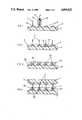
- FIG. 1is a sectional elevation of an electronic component, such as an integrated circuit chip, to which an interconnection wire is being bonded by means of a thermocompression wire bonder;
- FIG. 2is a sectional elevation of the IC chip shown in FIG. 1, having interconnection wires bonded to each contact;
- FIG. 3is a sectional elevation of an electronic component such as an IC chip carrier having a discrete quantity of a conductive material such as a solder located in a recess on each contact thereon;
- FIG. 4is a sectional elevation of the electronic components shown in FIGS. 2 and 3 interconnected by means of interconnection wires;
- FIG. 5is an enlarged view of a bonding head of a wire bonder in use forming an interconnection wire on a contact on an electronic component
- FIG. 6shows the bonding head shown in FIG. 5 being lifted from the contact, leaving an interconnection wire bonded to the contact.
- FIG. 1shows an electronic component 1 such as an integrated circuit chip having contacts 3 on a principal surface 5 thereof. Interconnection wires 7 are bonded to the contacts; one of the wires is shown in the process of being bonded to its respective contact by means of a wire bonder, of which only the capillary bonding head 9 is shown.
- the bonding headhas a through passage 11 through which the wire is supplied for bonding to the contacts on the component.
- the bonding headhas an aperture 13 in its side wall which communicates with the through passage 11 for housing means for weakening the wire at a point a predetermined distance from the opening through which the wire leaves the through passage.
- the wireis severed at a point a distance of from 2d to 20d above the ball 15 through which the wire is bonded to the contact, where d is the diameter of the wire.
- the wireis severed by applying force to the wire in a direction away from the contact so that it breaks at a point at which it has been weakened.
- FIG. 2shows the component 1 having interconnection wires 7 bonded to each of its contacts 3. Each of the wires has been severed so that the wires are all of substantially equal length. A layer 17 of an insulating material has been applied to the surface 5 of the component so as to encapsulate the bonds between the wires 7 and the contacts 3, including the balls 15 formed on the ends of the wires through which they are bonded to the contacts. A layer having the configuration shown in FIG. 2 may be of a relatively inflexible polymer such as one which is at least partly crystalline.
- FIG. 3shows an electronic component 21, such as an IC chip carrier, having contacts 23 on a principal surface 25 thereof. Pools 27 of conductive material such as solder are provided one on each contact 23. Each of the pools is located in a recess in a layer 29 of insulating layer which is located on the surface 25 of the component around each of the contacts 23. The ratio of the depth of each pool 27 of conductive material to its transverse dimension is at least 0.25.
- each recessis greater at the outer surface 31 of the layer 29 of insulating material than at the surface which contacts the surface 25 of the component 21, so that the recess is tapered inwardly towards its respective contact 23.
- the taper of the recesshelps to align the interconnection wires in the pools 27 of conductive material. This alignment can be further enhanced by severing each interconnection wire 7 on the component 1 such that it is tapered over a short distance at its free end.
- FIG. 4shows the first component 1 shown in FIG. 2, and the component 21, shown in FIG. 3, interconnected by means of the interconnection wires 7 which are bonded to the contacts 3 on the first component 1 as described above, and are connected to the contacts 23 on the second component 21 by means of the conductive material of the pools 27.
- the conductive materialis fusible, for example a solder
- the connection of the wires 7 to the contacts 23 on the second component 21is made by applying heat to cause the conductive material to fuse, and inserting the free ends of the wires 7 into the fused material.
- FIG. 5shows schematically a capillary bonding head 39 of a wire bonder in use forming a bond between the end of a wire 41 and a contact 43 on a surface of a component 45.
- the wire bondercomprises an electrode 47 for generating an arc between it and the end of the wire 41 which protrudes from the through passage 48 in the bonding head 39 when in a raised position (not shown).
- the electrode 47serves to form a ball 49 on the end of the wire 41 by causing the material of the wire to fuse.
- the electrodeis connected through a D.C. power source 50 to the wire 41.
- the bonding head 39is lowered, past the ball forming electrode 47, to apply heat and pressure to form a bond between the ball 49 and the contact 43.
- the bondis formed without the use of a material other than the materials of the wire and the contact, apart from incidental amounts of materials such as surface preparation agents, reaction products and contaminants.
- the wire 41is broken by gripping the wire within the wire bonder and applying a force to the wire in a direction substantially perpendicular to the contact 43 at the point at which the wire 41 is bonded thereto. As shown in FIG. 6, the force is applied by gripping the wire 41 and raising the wire bonded including the bonding head 39 form the contact 43.
- the forceis applied by gripping the wire 41 and raising the wire bonded including the bonding head 39 form the contact 43.
- the force to the wireby means of jaws which grip the wire and which are movable relative to the bonding arm.
- the jawsmay be mounted on a resilient arm which is capable of moving the jaws relative to the bonding arm so as to apply a reproducible force to the wire (which is bonded at its free end to the contact 43 via the ball 49).
- the wireis made to break under the applied force by weakening it at a desired point.
- the bonding headis provided with an electrode 51 in an aperture in the side wall of the head which communicates with the through passage 48.
- the electrode 51is connected to the wire 41 through the power source 50.
- the internal diameter of the through passage 48is arranged to be constant over a distance which is greater than 2.5x where x is the internal diameter of the passage at the point where the aperture and the passage meet. This allows the wire 41 to be cut more reproducibly to a desired length since its ability to move laterally in the passage is minimized; the arc between the electrode 51 and the wire 41 will therefore be shorter and more controllable.
- the combination of force and the arc between the wire 41 and the electrode 51produces an interconnection wire on the contact 43 that is tapered over a short distance 53 at its free end.
Landscapes
- Engineering & Computer Science (AREA)
- Computer Hardware Design (AREA)
- Microelectronics & Electronic Packaging (AREA)
- Power Engineering (AREA)
- Manufacturing & Machinery (AREA)
- Electric Connection Of Electric Components To Printed Circuits (AREA)
Abstract
Description
Claims (14)
Priority Applications (2)
| Application Number | Priority Date | Filing Date | Title |
|---|---|---|---|
| US07/151,131US4955523A (en) | 1986-12-17 | 1988-02-01 | Interconnection of electronic components |
| US07/713,024US5189507A (en) | 1986-12-17 | 1991-06-07 | Interconnection of electronic components |
Applications Claiming Priority (2)
| Application Number | Priority Date | Filing Date | Title |
|---|---|---|---|
| US94266586A | 1986-12-17 | 1986-12-17 | |
| US07/151,131US4955523A (en) | 1986-12-17 | 1988-02-01 | Interconnection of electronic components |
Related Parent Applications (3)
| Application Number | Title | Priority Date | Filing Date |
|---|---|---|---|
| US94266586AContinuation-In-Part | 1986-12-17 | 1986-12-17 | |
| US94266786AContinuation-In-Part | 1986-12-17 | 1986-12-17 | |
| US1555087AContinuation-In-Part | 1986-12-17 | 1987-02-13 |
Related Child Applications (1)
| Application Number | Title | Priority Date | Filing Date |
|---|---|---|---|
| US50350890ADivision | 1986-12-17 | 1990-04-02 |
Publications (1)
| Publication Number | Publication Date |
|---|---|
| US4955523Atrue US4955523A (en) | 1990-09-11 |
Family
ID=26848360
Family Applications (1)
| Application Number | Title | Priority Date | Filing Date |
|---|---|---|---|
| US07/151,131Expired - LifetimeUS4955523A (en) | 1986-12-17 | 1988-02-01 | Interconnection of electronic components |
Country Status (1)
| Country | Link |
|---|---|
| US (1) | US4955523A (en) |
Cited By (193)
| Publication number | Priority date | Publication date | Assignee | Title |
|---|---|---|---|---|
| US5090119A (en)* | 1987-12-08 | 1992-02-25 | Matsushita Electric Industrial Co., Ltd. | Method of forming an electrical contact bump |
| US5263246A (en)* | 1991-02-20 | 1993-11-23 | Nec Corporation | Bump forming method |
| US5298715A (en)* | 1992-04-27 | 1994-03-29 | International Business Machines Corporation | Lasersonic soldering of fine insulated wires to heat-sensitive substrates |
| US5349495A (en)* | 1989-06-23 | 1994-09-20 | Vlsi Technology, Inc. | System for securing and electrically connecting a semiconductor chip to a substrate |
| US5455390A (en)* | 1994-02-01 | 1995-10-03 | Tessera, Inc. | Microelectronics unit mounting with multiple lead bonding |
| US5476211A (en)* | 1993-11-16 | 1995-12-19 | Form Factor, Inc. | Method of manufacturing electrical contacts, using a sacrificial member |
| US5478007A (en)* | 1993-04-14 | 1995-12-26 | Amkor Electronics, Inc. | Method for interconnection of integrated circuit chip and substrate |
| US5518964A (en)* | 1994-07-07 | 1996-05-21 | Tessera, Inc. | Microelectronic mounting with multiple lead deformation and bonding |
| WO1996016440A1 (en)* | 1994-11-15 | 1996-05-30 | Formfactor, Inc. | Interconnection elements for microelectronic components |
| DE19641730A1 (en)* | 1995-10-30 | 1997-05-07 | Nat Semiconductor Corp | Bondable semiconductor device manufacture |
| US5635846A (en)* | 1992-10-19 | 1997-06-03 | International Business Machines Corporation | Test probe having elongated conductor embedded in an elostomeric material which is mounted on a space transformer |
| US5686842A (en)* | 1995-08-31 | 1997-11-11 | Nat Semiconductor Corp | Known good die test apparatus and method |
| US5688716A (en)* | 1994-07-07 | 1997-11-18 | Tessera, Inc. | Fan-out semiconductor chip assembly |
| US5733160A (en)* | 1996-03-01 | 1998-03-31 | Texas Instruments Incorporated | Method of forming spacers for a flat display apparatus |
| US5798286A (en)* | 1995-09-22 | 1998-08-25 | Tessera, Inc. | Connecting multiple microelectronic elements with lead deformation |
| WO1998041071A1 (en)* | 1997-03-11 | 1998-09-17 | Xemod, Inc. | Hybrid module assembling method and apparatus |
| US5810609A (en)* | 1995-08-28 | 1998-09-22 | Tessera, Inc. | Socket for engaging bump leads on a microelectronic device and methods therefor |
| US5820014A (en) | 1993-11-16 | 1998-10-13 | Form Factor, Inc. | Solder preforms |
| US5830782A (en)* | 1994-07-07 | 1998-11-03 | Tessera, Inc. | Microelectronic element bonding with deformation of leads in rows |
| US5864946A (en)* | 1993-11-16 | 1999-02-02 | Form Factor, Inc. | Method of making contact tip structures |
| US5884398A (en)* | 1993-11-16 | 1999-03-23 | Form Factor, Inc. | Mounting spring elements on semiconductor devices |
| US5906308A (en)* | 1996-08-21 | 1999-05-25 | Kabushiki Kaisha Shinkawa | Capillary for use in a wire bonding apparatus |
| US5917707A (en)* | 1993-11-16 | 1999-06-29 | Formfactor, Inc. | Flexible contact structure with an electrically conductive shell |
| US5938105A (en)* | 1997-01-15 | 1999-08-17 | National Semiconductor Corporation | Encapsulated ball bonding apparatus and method |
| US5983493A (en)* | 1993-11-16 | 1999-11-16 | Formfactor, Inc. | Method of temporarily, then permanently, connecting to a semiconductor device |
| US5989936A (en)* | 1994-07-07 | 1999-11-23 | Tessera, Inc. | Microelectronic assembly fabrication with terminal formation from a conductive layer |
| US5994152A (en) | 1996-02-21 | 1999-11-30 | Formfactor, Inc. | Fabricating interconnects and tips using sacrificial substrates |
| US6010059A (en)* | 1997-09-30 | 2000-01-04 | Siemens Energy & Automation, Inc. | Method for ultrasonic joining of electrical parts using a brazing alloy |
| US6049046A (en)* | 1997-09-30 | 2000-04-11 | Siemens Energy & Automation, Inc. | Electric circuit protection device having electrical parts ultrasonically joined using a brazing alloy |
| US6065667A (en)* | 1997-01-15 | 2000-05-23 | National Semiconductor Corporation | Method and apparatus for fine pitch wire bonding |
| US6104201A (en)* | 1996-11-08 | 2000-08-15 | International Business Machines Corporation | Method and apparatus for passive characterization of semiconductor substrates subjected to high energy (MEV) ion implementation using high-injection surface photovoltage |
| US6117694A (en)* | 1994-07-07 | 2000-09-12 | Tessera, Inc. | Flexible lead structures and methods of making same |
| US6133072A (en)* | 1996-12-13 | 2000-10-17 | Tessera, Inc. | Microelectronic connector with planar elastomer sockets |
| US6150186A (en)* | 1995-05-26 | 2000-11-21 | Formfactor, Inc. | Method of making a product with improved material properties by moderate heat-treatment of a metal incorporating a dilute additive |
| US6177636B1 (en) | 1994-12-29 | 2001-01-23 | Tessera, Inc. | Connection components with posts |
| US6213378B1 (en)* | 1997-01-15 | 2001-04-10 | National Semiconductor Corporation | Method and apparatus for ultra-fine pitch wire bonding |
| US6229199B1 (en)* | 1997-06-06 | 2001-05-08 | Rohm Co., Ltd. | Packaged semiconductor device |
| US6282780B1 (en)* | 1996-02-08 | 2001-09-04 | Matsushita Electric Industrial Co., Ltd. | Bump forming method and its forming apparatus. |
| US20010020545A1 (en)* | 1993-11-16 | 2001-09-13 | Formfactor, Inc. | Electrical contact structures formed by configuring a flexible wire to have a springable shape and overcoating the wire with at least one layer of a resilient conductive material, methods of mounting the contact structures to electronic components, and applications for employing the contact structures |
| US6316830B1 (en) | 1998-12-17 | 2001-11-13 | Charles Wen Chyang Lin | Bumpless flip chip assembly with strips and via-fill |
| US6336269B1 (en)* | 1993-11-16 | 2002-01-08 | Benjamin N. Eldridge | Method of fabricating an interconnection element |
| US6350633B1 (en) | 2000-08-22 | 2002-02-26 | Charles W. C. Lin | Semiconductor chip assembly with simultaneously electroplated contact terminal and connection joint |
| US6350386B1 (en) | 2000-09-20 | 2002-02-26 | Charles W. C. Lin | Method of making a support circuit with a tapered through-hole for a semiconductor chip assembly |
| US6350632B1 (en) | 2000-09-20 | 2002-02-26 | Charles W. C. Lin | Semiconductor chip assembly with ball bond connection joint |
| US6402970B1 (en) | 2000-08-22 | 2002-06-11 | Charles W. C. Lin | Method of making a support circuit for a semiconductor chip assembly |
| US6403400B2 (en) | 1998-12-17 | 2002-06-11 | Charles Wen Chyang Lin | Bumpless flip chip assembly with strips-in-via and plating |
| US6403460B1 (en) | 2000-08-22 | 2002-06-11 | Charles W. C. Lin | Method of making a semiconductor chip assembly |
| US6406939B1 (en) | 1998-05-02 | 2002-06-18 | Charles W. C. Lin | Flip chip assembly with via interconnection |
| US20020096787A1 (en)* | 1994-12-29 | 2002-07-25 | Tessera, Inc. | Connection components with posts |
| US6429112B1 (en) | 1994-07-07 | 2002-08-06 | Tessera, Inc. | Multi-layer substrates and fabrication processes |
| US6436734B1 (en) | 2000-08-22 | 2002-08-20 | Charles W. C. Lin | Method of making a support circuit for a semiconductor chip assembly |
| EP1232828A1 (en) | 1995-05-26 | 2002-08-21 | Formfactor, Inc. | Wire bonding, severing, and ball forming |
| US6440835B1 (en) | 2000-10-13 | 2002-08-27 | Charles W. C. Lin | Method of connecting a conductive trace to a semiconductor chip |
| US6439448B1 (en)* | 1999-11-05 | 2002-08-27 | Orthodyne Electronics Corporation | Large wire bonder head |
| US6444489B1 (en) | 2000-12-15 | 2002-09-03 | Charles W. C. Lin | Semiconductor chip assembly with bumped molded substrate |
| US6448644B1 (en) | 1998-05-02 | 2002-09-10 | Charles W. C. Lin | Flip chip assembly with via interconnection |
| US6448108B1 (en) | 2000-10-02 | 2002-09-10 | Charles W. C. Lin | Method of making a semiconductor chip assembly with a conductive trace subtractively formed before and after chip attachment |
| US6469394B1 (en) | 2000-01-31 | 2002-10-22 | Fujitsu Limited | Conductive interconnect structures and methods for forming conductive interconnect structures |
| US6492252B1 (en) | 2000-10-13 | 2002-12-10 | Bridge Semiconductor Corporation | Method of connecting a bumped conductive trace to a semiconductor chip |
| US20020190738A1 (en)* | 1993-04-30 | 2002-12-19 | Beaman Brian Samuel | Probe structure having a plurality of discrete insulated probe tips projecting from a support surface, apparatus for use thereof and methods of fabrication thereof |
| US6511865B1 (en) | 2000-09-20 | 2003-01-28 | Charles W. C. Lin | Method for forming a ball bond connection joint on a conductive trace and conductive pad in a semiconductor chip assembly |
| US6523255B2 (en)* | 2001-06-21 | 2003-02-25 | International Business Machines Corporation | Process and structure to repair damaged probes mounted on a space transformer |
| US20030038647A1 (en)* | 1995-11-09 | 2003-02-27 | Eldridge Benjamin N. | Probe card for probing wafers with raised contact elements |
| US6528891B2 (en) | 1998-12-17 | 2003-03-04 | Charles Wen Chyang Lin | Bumpless flip chip assembly with solder via |
| US6537851B1 (en) | 2000-10-13 | 2003-03-25 | Bridge Semiconductor Corporation | Method of connecting a bumped compliant conductive trace to a semiconductor chip |
| US6543674B2 (en) | 2001-02-06 | 2003-04-08 | Fujitsu Limited | Multilayer interconnection and method |
| US6544813B1 (en) | 2000-10-02 | 2003-04-08 | Charles W. C. Lin | Method of making a semiconductor chip assembly with a conductive trace subtractively formed before and after chip attachment |
| US6548393B1 (en) | 2000-10-13 | 2003-04-15 | Charles W. C. Lin | Semiconductor chip assembly with hardened connection joint |
| US20030071346A1 (en)* | 1994-07-07 | 2003-04-17 | Tessera, Inc. | Flexible lead structures and methods of making same |
| US6551861B1 (en) | 2000-08-22 | 2003-04-22 | Charles W. C. Lin | Method of making a semiconductor chip assembly by joining the chip to a support circuit with an adhesive |
| US6562709B1 (en) | 2000-08-22 | 2003-05-13 | Charles W. C. Lin | Semiconductor chip assembly with simultaneously electroplated contact terminal and connection joint |
| US6562657B1 (en) | 2000-08-22 | 2003-05-13 | Charles W. C. Lin | Semiconductor chip assembly with simultaneously electrolessly plated contact terminal and connection joint |
| US6576493B1 (en) | 2000-10-13 | 2003-06-10 | Bridge Semiconductor Corporation | Method of connecting a conductive trace and an insulative base to a semiconductor chip using multiple etch steps |
| US6576539B1 (en) | 2000-10-13 | 2003-06-10 | Charles W.C. Lin | Semiconductor chip assembly with interlocked conductive trace |
| US6583040B1 (en) | 2000-10-13 | 2003-06-24 | Bridge Semiconductor Corporation | Method of making a pillar in a laminated structure for a semiconductor chip assembly |
| US6581283B2 (en)* | 1999-12-02 | 2003-06-24 | Kabushiki Kaisha Shinkawa | Method for forming pin-form wires and the like |
| US6595405B2 (en)* | 2000-02-23 | 2003-07-22 | Fujikura, Ltd. | Connection structure and method for connecting printed circuit and metal terminal, and reinforcing structure and method for reinforcing junction therebetween |
| US6615485B2 (en) | 1993-11-16 | 2003-09-09 | Formfactor, Inc. | Probe card assembly and kit, and methods of making same |
| US6624648B2 (en) | 1993-11-16 | 2003-09-23 | Formfactor, Inc. | Probe card assembly |
| US6651322B1 (en)* | 2000-12-28 | 2003-11-25 | Unisys Corporation | Method of reworking a multilayer printed circuit board assembly |
| US6653170B1 (en) | 2001-02-06 | 2003-11-25 | Charles W. C. Lin | Semiconductor chip assembly with elongated wire ball bonded to chip and electrolessly plated to support circuit |
| US6660626B1 (en) | 2000-08-22 | 2003-12-09 | Charles W. C. Lin | Semiconductor chip assembly with simultaneously electrolessly plated contact terminal and connection joint |
| US6667229B1 (en) | 2000-10-13 | 2003-12-23 | Bridge Semiconductor Corporation | Method of connecting a bumped compliant conductive trace and an insulative base to a semiconductor chip |
| US20030234451A1 (en)* | 2002-06-25 | 2003-12-25 | Eli Razon | Stabilized wire bonded electrical connections and method of making same |
| US6687988B1 (en)* | 1999-10-20 | 2004-02-10 | Kabushiki Kaisha Shinkawa | Method for forming pin-form wires and the like |
| US6699780B1 (en) | 2000-10-13 | 2004-03-02 | Bridge Semiconductor Corporation | Method of connecting a conductive trace to a semiconductor chip using plasma undercut etching |
| US6727579B1 (en) | 1994-11-16 | 2004-04-27 | Formfactor, Inc. | Electrical contact structures formed by configuring a flexible wire to have a springable shape and overcoating the wire with at least one layer of a resilient conductive material, methods of mounting the contact structures to electronic components, and applications for employing the contact structures |
| US6740576B1 (en) | 2000-10-13 | 2004-05-25 | Bridge Semiconductor Corporation | Method of making a contact terminal with a plated metal peripheral sidewall portion for a semiconductor chip assembly |
| US20040169263A1 (en)* | 1996-12-12 | 2004-09-02 | Tessera, Inc. | Compliant package with conductive elastomeric posts |
| US20040222518A1 (en)* | 2003-02-25 | 2004-11-11 | Tessera, Inc. | Ball grid array with bumps |
| WO2004057648A3 (en)* | 2002-12-18 | 2005-02-17 | Acm Res Inc | Localized reflow for wire bonding and flip chip connections |
| US20050062492A1 (en)* | 2001-08-03 | 2005-03-24 | Beaman Brian Samuel | High density integrated circuit apparatus, test probe and methods of use thereof |
| US6872591B1 (en) | 2000-10-13 | 2005-03-29 | Bridge Semiconductor Corporation | Method of making a semiconductor chip assembly with a conductive trace and a substrate |
| US6876072B1 (en) | 2000-10-13 | 2005-04-05 | Bridge Semiconductor Corporation | Semiconductor chip assembly with chip in substrate cavity |
| US6908788B1 (en) | 2000-10-13 | 2005-06-21 | Bridge Semiconductor Corporation | Method of connecting a conductive trace to a semiconductor chip using a metal base |
| US6949408B1 (en) | 2000-10-13 | 2005-09-27 | Bridge Semiconductor Corporation | Method of connecting a conductive trace and an insulative base to a semiconductor chip using multiple etch steps |
| US20050221644A1 (en)* | 2003-02-04 | 2005-10-06 | Kieun Kim | Microprobe tips and methods for making |
| DE19723203B4 (en)* | 1996-06-20 | 2005-12-29 | LG Semicon Co., Ltd., Cheongju | Method for producing a chip-size semiconductor device |
| US6984576B1 (en) | 2000-10-13 | 2006-01-10 | Bridge Semiconductor Corporation | Method of connecting an additively and subtractively formed conductive trace and an insulative base to a semiconductor chip |
| US20060027899A1 (en)* | 2004-06-25 | 2006-02-09 | Tessera, Inc. | Structure with spherical contact pins |
| US7009297B1 (en) | 2000-10-13 | 2006-03-07 | Bridge Semiconductor Corporation | Semiconductor chip assembly with embedded metal particle |
| US20060051948A1 (en)* | 2003-02-04 | 2006-03-09 | Microfabrica Inc. | Microprobe tips and methods for making |
| US20060053625A1 (en)* | 2002-05-07 | 2006-03-16 | Microfabrica Inc. | Microprobe tips and methods for making |
| US20060112550A1 (en)* | 2002-05-07 | 2006-06-01 | Microfabrica Inc. | Microprobe tips and methods for making |
| US7071089B1 (en) | 2000-10-13 | 2006-07-04 | Bridge Semiconductor Corporation | Method of making a semiconductor chip assembly with a carved bumped terminal |
| US7075186B1 (en) | 2000-10-13 | 2006-07-11 | Bridge Semiconductor Corporation | Semiconductor chip assembly with interlocked contact terminal |
| US7084656B1 (en) | 1993-11-16 | 2006-08-01 | Formfactor, Inc. | Probe for semiconductor devices |
| US7094676B1 (en) | 2000-10-13 | 2006-08-22 | Bridge Semiconductor Corporation | Semiconductor chip assembly with embedded metal pillar |
| US7112521B1 (en) | 2000-10-13 | 2006-09-26 | Bridge Semiconductor Corporation | Method of making a semiconductor chip assembly with a bumped metal pillar |
| US7129113B1 (en) | 2000-10-13 | 2006-10-31 | Bridge Semiconductor Corporation | Method of making a three-dimensional stacked semiconductor package with a metal pillar in an encapsulant aperture |
| US7132741B1 (en) | 2000-10-13 | 2006-11-07 | Bridge Semiconductor Corporation | Semiconductor chip assembly with carved bumped terminal |
| US20060286829A1 (en)* | 2003-02-04 | 2006-12-21 | Microfabrica Inc. | Microprobe tips and methods for making |
| US20060289992A1 (en)* | 2005-06-27 | 2006-12-28 | Micron Technology, Inc. | Stacked semiconductor component, fabrication method and fabrication system |
| US7190080B1 (en) | 2000-10-13 | 2007-03-13 | Bridge Semiconductor Corporation | Semiconductor chip assembly with embedded metal pillar |
| US7200930B2 (en) | 1994-11-15 | 2007-04-10 | Formfactor, Inc. | Probe for semiconductor devices |
| US7262082B1 (en) | 2000-10-13 | 2007-08-28 | Bridge Semiconductor Corporation | Method of making a three-dimensional stacked semiconductor package with a metal pillar and a conductive interconnect in an encapsulant aperture |
| US7264991B1 (en) | 2000-10-13 | 2007-09-04 | Bridge Semiconductor Corporation | Method of connecting a conductive trace to a semiconductor chip using conductive adhesive |
| US20070205496A1 (en)* | 2004-06-25 | 2007-09-06 | Tessera, Inc. | Microelectronic packages and methods therefor |
| US7268421B1 (en) | 2004-11-10 | 2007-09-11 | Bridge Semiconductor Corporation | Semiconductor chip assembly with welded metal pillar that includes enlarged ball bond |
| US20070223195A1 (en)* | 2004-03-31 | 2007-09-27 | Mitsuo Honma | Method for Manufacturing a Heat Sink |
| US20070228110A1 (en)* | 1993-11-16 | 2007-10-04 | Formfactor, Inc. | Method Of Wirebonding That Utilizes A Gas Flow Within A Capillary From Which A Wire Is Played Out |
| US7319265B1 (en) | 2000-10-13 | 2008-01-15 | Bridge Semiconductor Corporation | Semiconductor chip assembly with precision-formed metal pillar |
| US20080108221A1 (en)* | 2003-12-31 | 2008-05-08 | Microfabrica Inc. | Microprobe Tips and Methods for Making |
| US20080116927A1 (en)* | 1993-11-16 | 2008-05-22 | Formfactor, Inc. | Contact tip structure for microelectronic interconnection elements and methods of making same |
| US20080150101A1 (en)* | 2006-12-20 | 2008-06-26 | Tessera, Inc. | Microelectronic packages having improved input/output connections and methods therefor |
| US7396703B1 (en) | 2003-11-20 | 2008-07-08 | Bridge Semiconductor Corporation | Method of making a semiconductor chip assembly with a bumped terminal and a filler |
| US7414319B2 (en) | 2000-10-13 | 2008-08-19 | Bridge Semiconductor Corporation | Semiconductor chip assembly with metal containment wall and solder terminal |
| US20080211524A1 (en)* | 2003-02-04 | 2008-09-04 | Microfabrica Inc. | Electrochemically Fabricated Microprobes |
| US7446419B1 (en) | 2004-11-10 | 2008-11-04 | Bridge Semiconductor Corporation | Semiconductor chip assembly with welded metal pillar of stacked metal balls |
| US7494843B1 (en) | 2006-12-26 | 2009-02-24 | Bridge Semiconductor Corporation | Method of making a semiconductor chip assembly with thermal conductor and encapsulant grinding |
| DE10023539B4 (en)* | 2000-05-13 | 2009-04-09 | Micronas Gmbh | Method for producing a component |
| US7538415B1 (en) | 2003-11-20 | 2009-05-26 | Bridge Semiconductor Corporation | Semiconductor chip assembly with bumped terminal, filler and insulative base |
| US20090256583A1 (en)* | 2003-02-04 | 2009-10-15 | Microfabrica Inc. | Vertical Microprobes for Contacting Electronic Components and Method for Making Such Probes |
| US7750483B1 (en) | 2004-11-10 | 2010-07-06 | Bridge Semiconductor Corporation | Semiconductor chip assembly with welded metal pillar and enlarged plated contact terminal |
| US20100175252A1 (en)* | 2007-08-22 | 2010-07-15 | Garcia Steven E | Automated Twist Pin Assembling Machine and Method for Interconnecting Stacked Circuit Boards in a Module |
| US7811863B1 (en) | 2006-10-26 | 2010-10-12 | Bridge Semiconductor Corporation | Method of making a semiconductor chip assembly with metal pillar and encapsulant grinding and heat sink attachment |
| US20100313414A1 (en)* | 2009-06-14 | 2010-12-16 | Terepac | Processes and structures for IC fabrication |
| US7993983B1 (en) | 2003-11-17 | 2011-08-09 | Bridge Semiconductor Corporation | Method of making a semiconductor chip assembly with chip and encapsulant grinding |
| US8373428B2 (en) | 1993-11-16 | 2013-02-12 | Formfactor, Inc. | Probe card assembly and kit, and methods of making same |
| US8485418B2 (en) | 1995-05-26 | 2013-07-16 | Formfactor, Inc. | Method of wirebonding that utilizes a gas flow within a capillary from which a wire is played out |
| US8540136B1 (en)* | 2012-09-06 | 2013-09-24 | Taiwan Semiconductor Manufacturing Company, Ltd. | Methods for stud bump formation and apparatus for performing the same |
| US8717054B2 (en) | 2003-02-04 | 2014-05-06 | Microfabrica Inc. | Methods of creating probe structures from a plurality of planar layers |
| US8772152B2 (en)* | 2012-02-24 | 2014-07-08 | Invensas Corporation | Method for package-on-package assembly with wire bonds to encapsulation surface |
| CN103943516A (en)* | 2014-04-14 | 2014-07-23 | 宁波芯健半导体有限公司 | Wafer level packaging method for wafer level convex blocks of laminated chips |
| WO2015039043A3 (en)* | 2013-09-16 | 2015-05-07 | Invensas Corporation | Microelectronic element with bond elements and compliant material layer |
| US9117811B2 (en) | 2011-06-13 | 2015-08-25 | Tessera, Inc. | Flip chip assembly and process with sintering material on metal bumps |
| US9137903B2 (en) | 2010-12-21 | 2015-09-15 | Tessera, Inc. | Semiconductor chip assembly and method for making same |
| CN105070666A (en)* | 2015-07-17 | 2015-11-18 | 北京中电科电子装备有限公司 | Chip, lead bonding method and device for packaging chip, and separating device for packaging chip |
| US9385052B2 (en) | 2012-09-14 | 2016-07-05 | STATS ChipPAC Pte. Ltd. | Semiconductor device and method of forming build-up interconnect structures over carrier for testing at interim stages |
| US9443797B2 (en) | 2012-09-14 | 2016-09-13 | STATS ChipPAC Pte. Ltd. | Semiconductor device having wire studs as vertical interconnect in FO-WLP |
| US9570416B2 (en) | 2004-11-03 | 2017-02-14 | Tessera, Inc. | Stacked packaging improvements |
| US9583411B2 (en) | 2014-01-17 | 2017-02-28 | Invensas Corporation | Fine pitch BVA using reconstituted wafer with area array accessible for testing |
| US9601454B2 (en) | 2013-02-01 | 2017-03-21 | Invensas Corporation | Method of forming a component having wire bonds and a stiffening layer |
| US9615456B2 (en) | 2012-12-20 | 2017-04-04 | Invensas Corporation | Microelectronic assembly for microelectronic packaging with bond elements to encapsulation surface |
| US9659848B1 (en) | 2015-11-18 | 2017-05-23 | Invensas Corporation | Stiffened wires for offset BVA |
| US9685365B2 (en) | 2013-08-08 | 2017-06-20 | Invensas Corporation | Method of forming a wire bond having a free end |
| US9691731B2 (en) | 2011-05-03 | 2017-06-27 | Tessera, Inc. | Package-on-package assembly with wire bonds to encapsulation surface |
| US9728527B2 (en) | 2013-11-22 | 2017-08-08 | Invensas Corporation | Multiple bond via arrays of different wire heights on a same substrate |
| US9735084B2 (en) | 2014-12-11 | 2017-08-15 | Invensas Corporation | Bond via array for thermal conductivity |
| US9761558B2 (en) | 2011-10-17 | 2017-09-12 | Invensas Corporation | Package-on-package assembly with wire bond vias |
| US9761554B2 (en) | 2015-05-07 | 2017-09-12 | Invensas Corporation | Ball bonding metal wire bond wires to metal pads |
| US20170317055A1 (en)* | 2016-05-02 | 2017-11-02 | International Business Machines Corporation | Integrated wafer-level processing system |
| US9812402B2 (en) | 2015-10-12 | 2017-11-07 | Invensas Corporation | Wire bond wires for interference shielding |
| US9818734B2 (en) | 2012-09-14 | 2017-11-14 | STATS ChipPAC Pte. Ltd. | Semiconductor device and method of forming build-up interconnect structures over a temporary substrate |
| US9831155B2 (en)* | 2016-03-11 | 2017-11-28 | Nanya Technology Corporation | Chip package having tilted through silicon via |
| US9842745B2 (en) | 2012-02-17 | 2017-12-12 | Invensas Corporation | Heat spreading substrate with embedded interconnects |
| US9852969B2 (en) | 2013-11-22 | 2017-12-26 | Invensas Corporation | Die stacks with one or more bond via arrays of wire bond wires and with one or more arrays of bump interconnects |
| US9888579B2 (en) | 2015-03-05 | 2018-02-06 | Invensas Corporation | Pressing of wire bond wire tips to provide bent-over tips |
| US9893017B2 (en) | 2015-04-09 | 2018-02-13 | STATS ChipPAC Pte. Ltd. | Double-sided semiconductor package and dual-mold method of making same |
| DE102016115221A1 (en)* | 2016-08-17 | 2018-02-22 | Karlsruher Institut für Technologie | Method for connecting at least two substrates to form a module |
| US9911718B2 (en) | 2015-11-17 | 2018-03-06 | Invensas Corporation | ‘RDL-First’ packaged microelectronic device for a package-on-package device |
| US9917073B2 (en) | 2012-07-31 | 2018-03-13 | Invensas Corporation | Reconstituted wafer-level package dram with conductive interconnects formed in encapsulant at periphery of the package |
| US9935075B2 (en) | 2016-07-29 | 2018-04-03 | Invensas Corporation | Wire bonding method and apparatus for electromagnetic interference shielding |
| US9953914B2 (en) | 2012-05-22 | 2018-04-24 | Invensas Corporation | Substrate-less stackable package with wire-bond interconnect |
| US9984992B2 (en) | 2015-12-30 | 2018-05-29 | Invensas Corporation | Embedded wire bond wires for vertical integration with separate surface mount and wire bond mounting surfaces |
| US9984901B2 (en) | 2005-12-23 | 2018-05-29 | Tessera, Inc. | Method for making a microelectronic assembly having conductive elements |
| US10008469B2 (en) | 2015-04-30 | 2018-06-26 | Invensas Corporation | Wafer-level packaging using wire bond wires in place of a redistribution layer |
| US10026717B2 (en) | 2013-11-22 | 2018-07-17 | Invensas Corporation | Multiple bond via arrays of different wire heights on a same substrate |
| US10128216B2 (en) | 2010-07-19 | 2018-11-13 | Tessera, Inc. | Stackable molded microelectronic packages |
| US10181457B2 (en) | 2015-10-26 | 2019-01-15 | Invensas Corporation | Microelectronic package for wafer-level chip scale packaging with fan-out |
| DE102012207560B4 (en) | 2012-05-07 | 2019-03-14 | Infineon Technologies Ag | METHOD FOR PRODUCING AND OPERATING A SEMICONDUCTOR MODULE |
| US10299368B2 (en) | 2016-12-21 | 2019-05-21 | Invensas Corporation | Surface integrated waveguides and circuit structures therefor |
| US10297582B2 (en) | 2012-08-03 | 2019-05-21 | Invensas Corporation | BVA interposer |
| US10332854B2 (en) | 2015-10-23 | 2019-06-25 | Invensas Corporation | Anchoring structure of fine pitch bva |
| US10381326B2 (en) | 2014-05-28 | 2019-08-13 | Invensas Corporation | Structure and method for integrated circuits packaging with increased density |
| US10416192B2 (en) | 2003-02-04 | 2019-09-17 | Microfabrica Inc. | Cantilever microprobes for contacting electronic components |
| US10460958B2 (en) | 2013-08-07 | 2019-10-29 | Invensas Corporation | Method of manufacturing embedded packaging with preformed vias |
| US10490528B2 (en) | 2015-10-12 | 2019-11-26 | Invensas Corporation | Embedded wire bond wires |
| US11262383B1 (en) | 2018-09-26 | 2022-03-01 | Microfabrica Inc. | Probes having improved mechanical and/or electrical properties for making contact between electronic circuit elements and methods for making |
| US20220199570A1 (en)* | 2020-12-18 | 2022-06-23 | Kulicke And Soffa Industries, Inc. | Methods of forming wire interconnect structures and related wire bonding tools |
| US20230187321A1 (en)* | 2021-12-15 | 2023-06-15 | Nxp Usa, Inc. | Leadless semiconductor package with shielded die-to-pad contacts |
| US20230271378A1 (en)* | 2022-02-25 | 2023-08-31 | Bell Textron Inc. | Break-wire conductor methods and systems |
| US12078657B2 (en) | 2019-12-31 | 2024-09-03 | Microfabrica Inc. | Compliant pin probes with extension springs, methods for making, and methods for using |
Citations (47)
| Publication number | Priority date | Publication date | Assignee | Title |
|---|---|---|---|---|
| US3075282A (en)* | 1959-07-24 | 1963-01-29 | Bell Telephone Labor Inc | Semiconductor device contact |
| US3202489A (en)* | 1959-12-01 | 1965-08-24 | Hughes Aircraft Co | Gold-aluminum alloy bond electrode attachment |
| US3286340A (en)* | 1964-02-28 | 1966-11-22 | Philco Corp | Fabrication of semiconductor units |
| US3296692A (en)* | 1963-09-13 | 1967-01-10 | Bell Telephone Labor Inc | Thermocompression wire attachments to quartz crystals |
| GB1056362A (en)* | 1964-03-31 | 1967-01-25 | Tempress Res Co | Improvements in or relating to electric lead wire bonding tools |
| US3373481A (en)* | 1965-06-22 | 1968-03-19 | Sperry Rand Corp | Method of electrically interconnecting conductors |
| US3392442A (en)* | 1965-06-24 | 1968-07-16 | Ibm | Solder method for providing standoff of device from substrate |
| US3397451A (en)* | 1966-04-06 | 1968-08-20 | Western Electric Co | Sequential wire and articlebonding methods |
| US3672047A (en)* | 1969-12-29 | 1972-06-27 | Hitachi Ltd | Method for bonding a conductive wire to a metal electrode |
| US3719981A (en)* | 1971-11-24 | 1973-03-13 | Rca Corp | Method of joining solder balls to solder bumps |
| US3811186A (en)* | 1972-12-11 | 1974-05-21 | Ibm | Method of aligning and attaching circuit devices on a substrate |
| US3921285A (en)* | 1974-07-15 | 1975-11-25 | Ibm | Method for joining microminiature components to a carrying structure |
| US4067104A (en)* | 1977-02-24 | 1978-01-10 | Rockwell International Corporation | Method of fabricating an array of flexible metallic interconnects for coupling microelectronics components |
| JPS5344901A (en)* | 1976-10-04 | 1978-04-22 | Ebara Corp | Output power detection system by fluid flange |
| US4142288A (en)* | 1976-02-28 | 1979-03-06 | Licentia Patent-Verwaltungs-G.M.B.H. | Method for contacting contact areas located on semiconductor bodies |
| JPS5583245A (en)* | 1978-12-19 | 1980-06-23 | Mitsubishi Electric Corp | Nail head bonding process |
| GB2036624A (en)* | 1978-10-19 | 1980-07-02 | Cii Honeywell Bull | Soldering together two elements arranged on opposite sides of a substrate |
| DD147293A1 (en)* | 1979-07-20 | 1981-03-25 | Frank Rudolf | DEVICE FOR NAIL HEAD WIRE BOND |
| US4326663A (en)* | 1978-07-20 | 1982-04-27 | Eltec Instruments, Inc. | Pyroelectric detector |
| US4332341A (en)* | 1979-12-26 | 1982-06-01 | Bell Telephone Laboratories, Incorporated | Fabrication of circuit packages using solid phase solder bonding |
| JPS57155736A (en)* | 1981-03-23 | 1982-09-25 | Hitachi Ltd | Wire bonder |
| US4374457A (en)* | 1980-08-04 | 1983-02-22 | Wiech Raymond E Jr | Method of fabricating complex micro-circuit boards and substrates |
| US4412642A (en)* | 1982-03-15 | 1983-11-01 | Western Electric Co., Inc. | Cast solder leads for leadless semiconductor circuits |
| US4417392A (en)* | 1980-05-15 | 1983-11-29 | Cts Corporation | Process of making multi-layer ceramic package |
| US4419818A (en)* | 1981-10-26 | 1983-12-13 | Amp Incorporated | Method for manufacturing substrate with selectively trimmable resistors between signal leads and ground structure |
| US4422568A (en)* | 1981-01-12 | 1983-12-27 | Kulicke And Soffa Industries, Inc. | Method of making constant bonding wire tail lengths |
| JPS5929496A (en)* | 1982-08-10 | 1984-02-16 | 松下電器産業株式会社 | How to solder multi-leg electronic components |
| JPS5933249A (en)* | 1982-08-19 | 1984-02-23 | Asahi Chem Ind Co Ltd | Acrylamide manufacturing method |
| US4442938A (en)* | 1983-03-22 | 1984-04-17 | Advanced Interconnections | Socket terminal positioning method and construction |
| US4447857A (en)* | 1981-12-09 | 1984-05-08 | International Business Machines Corporation | Substrate with multiple type connections |
| DE3305952A1 (en)* | 1983-02-21 | 1984-08-23 | ETA S.A. Fabriques d'Ebauches, Granges | Method of mounting an integrated circuit panel on a substrate |
| JPS59208751A (en)* | 1983-05-13 | 1984-11-27 | Hitachi Ltd | Formation of bump |
| GB2142568A (en)* | 1983-06-30 | 1985-01-23 | Raychem Corp | Assembly of electronic components |
| JPS6076934A (en)* | 1983-10-04 | 1985-05-01 | Nec Corp | Method automatically inserting fitting parts |
| JPS6089951A (en)* | 1983-10-24 | 1985-05-20 | Nec Corp | Manufacture of flip chip ic |
| US4520561A (en)* | 1983-12-16 | 1985-06-04 | Rca Corporation | Method of fabricating an electronic circuit including an aperture through the substrate thereof |
| JPS60134444A (en)* | 1983-12-23 | 1985-07-17 | Hitachi Ltd | Formation for bump electrode |
| GB2151529A (en)* | 1983-12-19 | 1985-07-24 | American Telephone & Telegraph | Method for making electrical contact to semiconductor devices |
| US4542438A (en)* | 1981-09-07 | 1985-09-17 | Toshiba Corporation | Hybrid integrated circuit device |
| US4547833A (en)* | 1983-12-23 | 1985-10-15 | Schlumberger Technology Corporation | High density electronics packaging system for hostile environment |
| JPS6191939A (en)* | 1984-10-12 | 1986-05-10 | Toshiba Corp | Torch for semiconductor wire bonding |
| US4641426A (en)* | 1985-06-21 | 1987-02-10 | Associated Enterprises, Inc. | Surface mount compatible connector system with mechanical integrity |
| US4661192A (en)* | 1985-08-22 | 1987-04-28 | Motorola, Inc. | Low cost integrated circuit bonding process |
| US4708885A (en)* | 1985-11-22 | 1987-11-24 | Murata Manufacturing Co., Ltd. | Manufacturing method for an electronic component |
| US4732313A (en)* | 1984-07-27 | 1988-03-22 | Kabushiki Kaisha Toshiba | Apparatus and method for manufacturing semiconductor device |
| US4746300A (en)* | 1985-06-10 | 1988-05-24 | Gilles Thevenin | Mounting panel for removable elements |
| US4818728A (en)* | 1986-12-03 | 1989-04-04 | Sharp Kabushiki Kaisha | Method of making a hybrid semiconductor device |
- 1988
- 1988-02-01USUS07/151,131patent/US4955523A/ennot_activeExpired - Lifetime
Patent Citations (47)
| Publication number | Priority date | Publication date | Assignee | Title |
|---|---|---|---|---|
| US3075282A (en)* | 1959-07-24 | 1963-01-29 | Bell Telephone Labor Inc | Semiconductor device contact |
| US3202489A (en)* | 1959-12-01 | 1965-08-24 | Hughes Aircraft Co | Gold-aluminum alloy bond electrode attachment |
| US3296692A (en)* | 1963-09-13 | 1967-01-10 | Bell Telephone Labor Inc | Thermocompression wire attachments to quartz crystals |
| US3286340A (en)* | 1964-02-28 | 1966-11-22 | Philco Corp | Fabrication of semiconductor units |
| GB1056362A (en)* | 1964-03-31 | 1967-01-25 | Tempress Res Co | Improvements in or relating to electric lead wire bonding tools |
| US3373481A (en)* | 1965-06-22 | 1968-03-19 | Sperry Rand Corp | Method of electrically interconnecting conductors |
| US3392442A (en)* | 1965-06-24 | 1968-07-16 | Ibm | Solder method for providing standoff of device from substrate |
| US3397451A (en)* | 1966-04-06 | 1968-08-20 | Western Electric Co | Sequential wire and articlebonding methods |
| US3672047A (en)* | 1969-12-29 | 1972-06-27 | Hitachi Ltd | Method for bonding a conductive wire to a metal electrode |
| US3719981A (en)* | 1971-11-24 | 1973-03-13 | Rca Corp | Method of joining solder balls to solder bumps |
| US3811186A (en)* | 1972-12-11 | 1974-05-21 | Ibm | Method of aligning and attaching circuit devices on a substrate |
| US3921285A (en)* | 1974-07-15 | 1975-11-25 | Ibm | Method for joining microminiature components to a carrying structure |
| US4142288A (en)* | 1976-02-28 | 1979-03-06 | Licentia Patent-Verwaltungs-G.M.B.H. | Method for contacting contact areas located on semiconductor bodies |
| JPS5344901A (en)* | 1976-10-04 | 1978-04-22 | Ebara Corp | Output power detection system by fluid flange |
| US4067104A (en)* | 1977-02-24 | 1978-01-10 | Rockwell International Corporation | Method of fabricating an array of flexible metallic interconnects for coupling microelectronics components |
| US4326663A (en)* | 1978-07-20 | 1982-04-27 | Eltec Instruments, Inc. | Pyroelectric detector |
| GB2036624A (en)* | 1978-10-19 | 1980-07-02 | Cii Honeywell Bull | Soldering together two elements arranged on opposite sides of a substrate |
| JPS5583245A (en)* | 1978-12-19 | 1980-06-23 | Mitsubishi Electric Corp | Nail head bonding process |
| DD147293A1 (en)* | 1979-07-20 | 1981-03-25 | Frank Rudolf | DEVICE FOR NAIL HEAD WIRE BOND |
| US4332341A (en)* | 1979-12-26 | 1982-06-01 | Bell Telephone Laboratories, Incorporated | Fabrication of circuit packages using solid phase solder bonding |
| US4417392A (en)* | 1980-05-15 | 1983-11-29 | Cts Corporation | Process of making multi-layer ceramic package |
| US4374457A (en)* | 1980-08-04 | 1983-02-22 | Wiech Raymond E Jr | Method of fabricating complex micro-circuit boards and substrates |
| US4422568A (en)* | 1981-01-12 | 1983-12-27 | Kulicke And Soffa Industries, Inc. | Method of making constant bonding wire tail lengths |
| JPS57155736A (en)* | 1981-03-23 | 1982-09-25 | Hitachi Ltd | Wire bonder |
| US4542438A (en)* | 1981-09-07 | 1985-09-17 | Toshiba Corporation | Hybrid integrated circuit device |
| US4419818A (en)* | 1981-10-26 | 1983-12-13 | Amp Incorporated | Method for manufacturing substrate with selectively trimmable resistors between signal leads and ground structure |
| US4447857A (en)* | 1981-12-09 | 1984-05-08 | International Business Machines Corporation | Substrate with multiple type connections |
| US4412642A (en)* | 1982-03-15 | 1983-11-01 | Western Electric Co., Inc. | Cast solder leads for leadless semiconductor circuits |
| JPS5929496A (en)* | 1982-08-10 | 1984-02-16 | 松下電器産業株式会社 | How to solder multi-leg electronic components |
| JPS5933249A (en)* | 1982-08-19 | 1984-02-23 | Asahi Chem Ind Co Ltd | Acrylamide manufacturing method |
| DE3305952A1 (en)* | 1983-02-21 | 1984-08-23 | ETA S.A. Fabriques d'Ebauches, Granges | Method of mounting an integrated circuit panel on a substrate |
| US4442938A (en)* | 1983-03-22 | 1984-04-17 | Advanced Interconnections | Socket terminal positioning method and construction |
| JPS59208751A (en)* | 1983-05-13 | 1984-11-27 | Hitachi Ltd | Formation of bump |
| GB2142568A (en)* | 1983-06-30 | 1985-01-23 | Raychem Corp | Assembly of electronic components |
| JPS6076934A (en)* | 1983-10-04 | 1985-05-01 | Nec Corp | Method automatically inserting fitting parts |
| JPS6089951A (en)* | 1983-10-24 | 1985-05-20 | Nec Corp | Manufacture of flip chip ic |
| US4520561A (en)* | 1983-12-16 | 1985-06-04 | Rca Corporation | Method of fabricating an electronic circuit including an aperture through the substrate thereof |
| GB2151529A (en)* | 1983-12-19 | 1985-07-24 | American Telephone & Telegraph | Method for making electrical contact to semiconductor devices |
| JPS60134444A (en)* | 1983-12-23 | 1985-07-17 | Hitachi Ltd | Formation for bump electrode |
| US4547833A (en)* | 1983-12-23 | 1985-10-15 | Schlumberger Technology Corporation | High density electronics packaging system for hostile environment |
| US4732313A (en)* | 1984-07-27 | 1988-03-22 | Kabushiki Kaisha Toshiba | Apparatus and method for manufacturing semiconductor device |
| JPS6191939A (en)* | 1984-10-12 | 1986-05-10 | Toshiba Corp | Torch for semiconductor wire bonding |
| US4746300A (en)* | 1985-06-10 | 1988-05-24 | Gilles Thevenin | Mounting panel for removable elements |
| US4641426A (en)* | 1985-06-21 | 1987-02-10 | Associated Enterprises, Inc. | Surface mount compatible connector system with mechanical integrity |
| US4661192A (en)* | 1985-08-22 | 1987-04-28 | Motorola, Inc. | Low cost integrated circuit bonding process |
| US4708885A (en)* | 1985-11-22 | 1987-11-24 | Murata Manufacturing Co., Ltd. | Manufacturing method for an electronic component |
| US4818728A (en)* | 1986-12-03 | 1989-04-04 | Sharp Kabushiki Kaisha | Method of making a hybrid semiconductor device |
Non-Patent Citations (5)
| Title |
|---|
| IBM Technical Disclosure, "Chip-to-Pin Carrier Interconnection Systems", Ng, vol. 21, No. 7, pp. 2707, 2708, Dec. 1978. |
| IBM Technical Disclosure, B. W. Miller, Cutting Fine Lead Wires . . . , vol. 10, No. 3, Aug. 1967, p. 190.* |
| IBM Technical Disclosure, Chip to Pin Carrier Interconnection Systems , Ng, vol. 21, No. 7, pp. 2707, 2708, Dec. 1978.* |
| Low Cost Pin Grid Array Packages (Solid State Technology, May 1985, pp. 239 to 241).* |
| New Semiconductor Bonding Technique, (Electronic Technician, Sep. 1957, p. 71).* |
Cited By (384)
| Publication number | Priority date | Publication date | Assignee | Title |
|---|---|---|---|---|
| US5090119A (en)* | 1987-12-08 | 1992-02-25 | Matsushita Electric Industrial Co., Ltd. | Method of forming an electrical contact bump |
| US5349495A (en)* | 1989-06-23 | 1994-09-20 | Vlsi Technology, Inc. | System for securing and electrically connecting a semiconductor chip to a substrate |
| US5263246A (en)* | 1991-02-20 | 1993-11-23 | Nec Corporation | Bump forming method |
| US5298715A (en)* | 1992-04-27 | 1994-03-29 | International Business Machines Corporation | Lasersonic soldering of fine insulated wires to heat-sensitive substrates |
| US20080117613A1 (en)* | 1992-10-19 | 2008-05-22 | International Business Machines Corporation | High density integrated circuit apparatus, test probe and methods of use thereof |
| US20080048697A1 (en)* | 1992-10-19 | 2008-02-28 | International Business Machines Corporation | High density integrated circuit apparatus, test probe and methods of use thereof |
| US20100045318A1 (en)* | 1992-10-19 | 2010-02-25 | International Business Machines Corporation | High density integrated circuit apparatus, test probe and methods of use thereof |
| US20100045317A1 (en)* | 1992-10-19 | 2010-02-25 | International Business Machines Corporation | High density integrated circuit apparatus, test probe and methods of use thereof |
| US20100045321A1 (en)* | 1992-10-19 | 2010-02-25 | International Business Machines Corporation | High density integrated circuit apparatus, test probe and methods of use thereof |
| US20100045320A1 (en)* | 1992-10-19 | 2010-02-25 | International Business Machines Corporation | High density integrated circuit apparatus, test probe and methods of use thereof |
| US5635846A (en)* | 1992-10-19 | 1997-06-03 | International Business Machines Corporation | Test probe having elongated conductor embedded in an elostomeric material which is mounted on a space transformer |
| US20070271781A9 (en)* | 1992-10-19 | 2007-11-29 | Beaman Brian S | High density integrated circuit apparatus, test probe and methods of use thereof |
| US20080048690A1 (en)* | 1992-10-19 | 2008-02-28 | International Business Machines Corporation | High density integrated circuit apparatus, test probe and methods of use thereof |
| US20080116913A1 (en)* | 1992-10-19 | 2008-05-22 | International Business Machines Corporation | High density integrated circuit apparatus, test probe and methods of use thereof |
| US20080100318A1 (en)* | 1992-10-19 | 2008-05-01 | International Business Machines Corporation | High density integrated circuit apparatus, test probe and methods of use thereof |
| US7538565B1 (en)* | 1992-10-19 | 2009-05-26 | International Business Machines Corporation | High density integrated circuit apparatus, test probe and methods of use thereof |
| US20080048691A1 (en)* | 1992-10-19 | 2008-02-28 | International Business Machines Corporation | High density integrated circuit apparatus, test probe and methods of use thereof |
| US20100052715A1 (en)* | 1992-10-19 | 2010-03-04 | International Business Machines Corporation | High density integrated circuit apparatus, test probe and methods of use thereof |
| US20080047741A1 (en)* | 1992-10-19 | 2008-02-28 | International Business Machines Corporation | High density integrated circuit apparatus, test probe and methods of use thereof |
| US20090128176A1 (en)* | 1992-10-19 | 2009-05-21 | Brian Samuel Beaman | High density integrated circuit apparatus, test probe and methods of use thereof |
| US20080129320A1 (en)* | 1992-10-19 | 2008-06-05 | International Business Machines Corporation | High density integrated circuit apparatus, test probe and methods of use thereof |
| US20080132094A1 (en)* | 1992-10-19 | 2008-06-05 | International Business Machines Corporation | High density integrated circuit apparatus, test probe and methods of use thereof |
| US20080129319A1 (en)* | 1992-10-19 | 2008-06-05 | International Business Machines Corporation | High density integrated circuit apparatus, test probe and methods of use thereof |
| US20080106285A1 (en)* | 1992-10-19 | 2008-05-08 | International Business Machines Corporation | High density integrated circuit apparatus, test probe and methods of use thereof |
| US20080121879A1 (en)* | 1992-10-19 | 2008-05-29 | Brian Samuel Beaman | High density integrated circuit apparatus, test probe and methods of use thereof |
| US20080123310A1 (en)* | 1992-10-19 | 2008-05-29 | International Business Machines Corporation | High density integrated circuit apparatus, test probe and methods of use thereof |
| US20100045324A1 (en)* | 1992-10-19 | 2010-02-25 | International Business Machines Corporation | High density integrated circuit apparatus, test probe and methods of use thereof |
| US20080106872A1 (en)* | 1992-10-19 | 2008-05-08 | International Business Machines Corporation | High density integrated circuit apparatus, test probe and methods of use thereof |
| US20090315579A1 (en)* | 1992-10-19 | 2009-12-24 | International Business Machines Corporation | High density integrated circuit apparatus, test probe and methods of use thereof |
| US20080117611A1 (en)* | 1992-10-19 | 2008-05-22 | International Business Machines Corporation | High density integrated circuit apparatus, test probe and methods of use thereof |
| US20080116912A1 (en)* | 1992-10-19 | 2008-05-22 | International Business Machines Corporation | High density integrated circuit apparatus, test probe and methods of use thereof |
| US20080117612A1 (en)* | 1992-10-19 | 2008-05-22 | International Business Machines Corporation | High density integrated circuit apparatus, test probe and methods of use thereof |
| US20080112144A1 (en)* | 1992-10-19 | 2008-05-15 | International Business Machines Corporation | High density integrated circuit apparatus, test probe and methods of use thereof |
| US20080112145A1 (en)* | 1992-10-19 | 2008-05-15 | International Business Machines Corporation | High density integrated circuit apparatus, test probe and methods of use thereof |
| US20080111570A1 (en)* | 1992-10-19 | 2008-05-15 | International Business Machines Corporation | High density integrated circuit apparatus, test probe and methods of use thereof |
| US20080100317A1 (en)* | 1992-10-19 | 2008-05-01 | International Business Machines Corporation | High density integrated circuit apparatus, test probe and methods of use thereof |
| US20080112146A1 (en)* | 1992-10-19 | 2008-05-15 | International Business Machines Corporation | High density integrated circuit apparatus, test probe and methods of use thereof |
| US20080100316A1 (en)* | 1992-10-19 | 2008-05-01 | International Business Machines Corporation | High density integrated circuit apparatus, test probe and methods of use thereof |
| US20080112148A1 (en)* | 1992-10-19 | 2008-05-15 | International Business Machines Corporation | High density integrated circuit apparatus, test probe and methods of use thereof |
| US20080111569A1 (en)* | 1992-10-19 | 2008-05-15 | International Business Machines Corporation | High density integrated circuit apparatus, test probe and methods of use thereof |
| US20080112149A1 (en)* | 1992-10-19 | 2008-05-15 | International Business Machines Corporation | High density integrated circuit apparatus, test probe and methods of use thereof |
| US20080112147A1 (en)* | 1992-10-19 | 2008-05-15 | International Business Machines Corporation | High density integrated circuit apparatus, test probe and methods of use thereof |
| US6334247B1 (en)* | 1992-10-19 | 2002-01-01 | International Business Machines Corporation | High density integrated circuit apparatus, test probe and methods of use thereof |
| US20020014004A1 (en)* | 1992-10-19 | 2002-02-07 | Beaman Brian Samuel | High density integrated circuit apparatus, test probe and methods of use thereof |
| US20080106291A1 (en)* | 1992-10-19 | 2008-05-08 | Beaman Brian S | High density integrated circuit apparatus, test probe and methods of use thereof |
| US20080106281A1 (en)* | 1992-10-19 | 2008-05-08 | International Business Machines Corporation | High density integrated circuit apparatus, test probe and methods of use thereof |
| US20080106284A1 (en)* | 1992-10-19 | 2008-05-08 | International Business Machines Corporation | High density integrated circuit apparatus, test probe and methods of use thereof |
| US20080106282A1 (en)* | 1992-10-19 | 2008-05-08 | International Business Machines Corporation | High density integrated circuit apparatus, test probe and methods of use thereof |
| US20080106283A1 (en)* | 1992-10-19 | 2008-05-08 | International Business Machines Corporation | High density integrated circuit apparatus, test probe and methods of use thereof |
| US5478007A (en)* | 1993-04-14 | 1995-12-26 | Amkor Electronics, Inc. | Method for interconnection of integrated circuit chip and substrate |
| US7368924B2 (en)* | 1993-04-30 | 2008-05-06 | International Business Machines Corporation | Probe structure having a plurality of discrete insulated probe tips projecting from a support surface, apparatus for use thereof and methods of fabrication thereof |
| US20020190738A1 (en)* | 1993-04-30 | 2002-12-19 | Beaman Brian Samuel | Probe structure having a plurality of discrete insulated probe tips projecting from a support surface, apparatus for use thereof and methods of fabrication thereof |
| US5917707A (en)* | 1993-11-16 | 1999-06-29 | Formfactor, Inc. | Flexible contact structure with an electrically conductive shell |
| US20030062398A1 (en)* | 1993-11-16 | 2003-04-03 | Formfactor, Inc. | Method for manufacturing raised electrical contact pattern of controlled geometry |
| US6274823B1 (en) | 1993-11-16 | 2001-08-14 | Formfactor, Inc. | Interconnection substrates with resilient contact structures on both sides |
| US7082682B2 (en) | 1993-11-16 | 2006-08-01 | Formfactor, Inc. | Contact structures and methods for making same |
| US20010002624A1 (en)* | 1993-11-16 | 2001-06-07 | Igor Y. Khandros | Tip structures. |
| US20010020545A1 (en)* | 1993-11-16 | 2001-09-13 | Formfactor, Inc. | Electrical contact structures formed by configuring a flexible wire to have a springable shape and overcoating the wire with at least one layer of a resilient conductive material, methods of mounting the contact structures to electronic components, and applications for employing the contact structures |
| US6615485B2 (en) | 1993-11-16 | 2003-09-09 | Formfactor, Inc. | Probe card assembly and kit, and methods of making same |
| US7084656B1 (en) | 1993-11-16 | 2006-08-01 | Formfactor, Inc. | Probe for semiconductor devices |
| US6215670B1 (en) | 1993-11-16 | 2001-04-10 | Formfactor, Inc. | Method for manufacturing raised electrical contact pattern of controlled geometry |
| US6336269B1 (en)* | 1993-11-16 | 2002-01-08 | Benjamin N. Eldridge | Method of fabricating an interconnection element |
| US7086149B2 (en) | 1993-11-16 | 2006-08-08 | Formfactor, Inc. | Method of making a contact structure with a distinctly formed tip structure |
| US5476211A (en)* | 1993-11-16 | 1995-12-19 | Form Factor, Inc. | Method of manufacturing electrical contacts, using a sacrificial member |
| US20070228110A1 (en)* | 1993-11-16 | 2007-10-04 | Formfactor, Inc. | Method Of Wirebonding That Utilizes A Gas Flow Within A Capillary From Which A Wire Is Played Out |
| US6655023B1 (en) | 1993-11-16 | 2003-12-02 | Formfactor, Inc. | Method and apparatus for burning-in semiconductor devices in wafer form |
| US7142000B2 (en) | 1993-11-16 | 2006-11-28 | Formfactor, Inc. | Mounting spring elements on semiconductor devices, and wafer-level testing methodology |
| US7225538B2 (en) | 1993-11-16 | 2007-06-05 | Formfactor, Inc. | Resilient contact structures formed and then attached to a substrate |
| US6049976A (en)* | 1993-11-16 | 2000-04-18 | Formfactor, Inc. | Method of mounting free-standing resilient electrical contact structures to electronic components |
| US5820014A (en) | 1993-11-16 | 1998-10-13 | Form Factor, Inc. | Solder preforms |
| US6032356A (en)* | 1993-11-16 | 2000-03-07 | Formfactor. Inc. | Wafer-level test and burn-in, and semiconductor process |
| US6778406B2 (en) | 1993-11-16 | 2004-08-17 | Formfactor, Inc. | Resilient contact structures for interconnecting electronic devices |
| US6538214B2 (en) | 1993-11-16 | 2003-03-25 | Formfactor, Inc. | Method for manufacturing raised electrical contact pattern of controlled geometry |
| US20070046313A1 (en)* | 1993-11-16 | 2007-03-01 | Formfactor, Inc. | Mounting Spring Elements on Semiconductor Devices, and Wafer-Level Testing Methodology |
| US20080116927A1 (en)* | 1993-11-16 | 2008-05-22 | Formfactor, Inc. | Contact tip structure for microelectronic interconnection elements and methods of making same |
| US5852871A (en)* | 1993-11-16 | 1998-12-29 | Form Factor, Inc. | Method of making raised contacts on electronic components |
| US5983493A (en)* | 1993-11-16 | 1999-11-16 | Formfactor, Inc. | Method of temporarily, then permanently, connecting to a semiconductor device |
| US6818840B2 (en) | 1993-11-16 | 2004-11-16 | Formfactor, Inc. | Method for manufacturing raised electrical contact pattern of controlled geometry |
| US20020117330A1 (en)* | 1993-11-16 | 2002-08-29 | Formfactor, Inc. | Resilient contact structures formed and then attached to a substrate |
| US6624648B2 (en) | 1993-11-16 | 2003-09-23 | Formfactor, Inc. | Probe card assembly |
| US5864946A (en)* | 1993-11-16 | 1999-02-02 | Form Factor, Inc. | Method of making contact tip structures |
| US8373428B2 (en) | 1993-11-16 | 2013-02-12 | Formfactor, Inc. | Probe card assembly and kit, and methods of making same |
| US6835898B2 (en) | 1993-11-16 | 2004-12-28 | Formfactor, Inc. | Electrical contact structures formed by configuring a flexible wire to have a springable shape and overcoating the wire with at least one layer of a resilient conductive material, methods of mounting the contact structures to electronic components, and applications for employing the contact structures |
| US5884398A (en)* | 1993-11-16 | 1999-03-23 | Form Factor, Inc. | Mounting spring elements on semiconductor devices |
| US6044548A (en)* | 1994-02-01 | 2000-04-04 | Tessera, Inc. | Methods of making connections to a microelectronic unit |
| US5455390A (en)* | 1994-02-01 | 1995-10-03 | Tessera, Inc. | Microelectronics unit mounting with multiple lead bonding |
| US5794330A (en)* | 1994-02-01 | 1998-08-18 | Tessera, Inc. | Microelectronics unit mounting with multiple lead bonding |
| US5801441A (en)* | 1994-07-07 | 1998-09-01 | Tessera, Inc. | Microelectronic mounting with multiple lead deformation and bonding |
| US6828668B2 (en) | 1994-07-07 | 2004-12-07 | Tessera, Inc. | Flexible lead structures and methods of making same |
| US5830782A (en)* | 1994-07-07 | 1998-11-03 | Tessera, Inc. | Microelectronic element bonding with deformation of leads in rows |
| US6429112B1 (en) | 1994-07-07 | 2002-08-06 | Tessera, Inc. | Multi-layer substrates and fabrication processes |
| US7166914B2 (en) | 1994-07-07 | 2007-01-23 | Tessera, Inc. | Semiconductor package with heat sink |
| US6307260B1 (en) | 1994-07-07 | 2001-10-23 | Tessera, Inc. | Microelectronic assembly fabrication with terminal formation from a conductive layer |
| US6265765B1 (en) | 1994-07-07 | 2001-07-24 | Tessera, Inc. | Fan-out semiconductor chip assembly |
| US5959354A (en)* | 1994-07-07 | 1999-09-28 | Tessera, Inc. | Connection components with rows of lead bond sections |
| US6080603A (en)* | 1994-07-07 | 2000-06-27 | Tessera, Inc. | Fixtures and methods for lead bonding and deformation |
| US5913109A (en)* | 1994-07-07 | 1999-06-15 | Tessera, Inc. | Fixtures and methods for lead bonding and deformation |
| US20030071346A1 (en)* | 1994-07-07 | 2003-04-17 | Tessera, Inc. | Flexible lead structures and methods of making same |
| US5989936A (en)* | 1994-07-07 | 1999-11-23 | Tessera, Inc. | Microelectronic assembly fabrication with terminal formation from a conductive layer |
| US6104087A (en)* | 1994-07-07 | 2000-08-15 | Tessera, Inc. | Microelectronic assemblies with multiple leads |
| US5688716A (en)* | 1994-07-07 | 1997-11-18 | Tessera, Inc. | Fan-out semiconductor chip assembly |
| US6117694A (en)* | 1994-07-07 | 2000-09-12 | Tessera, Inc. | Flexible lead structures and methods of making same |
| US6635553B1 (en) | 1994-07-07 | 2003-10-21 | Iessera, Inc. | Microelectronic assemblies with multiple leads |
| US5518964A (en)* | 1994-07-07 | 1996-05-21 | Tessera, Inc. | Microelectronic mounting with multiple lead deformation and bonding |
| US6194291B1 (en) | 1994-07-07 | 2001-02-27 | Tessera, Inc. | Microelectronic assemblies with multiple leads |
| WO1996016440A1 (en)* | 1994-11-15 | 1996-05-30 | Formfactor, Inc. | Interconnection elements for microelectronic components |
| US7200930B2 (en) | 1994-11-15 | 2007-04-10 | Formfactor, Inc. | Probe for semiconductor devices |
| US6727579B1 (en) | 1994-11-16 | 2004-04-27 | Formfactor, Inc. | Electrical contact structures formed by configuring a flexible wire to have a springable shape and overcoating the wire with at least one layer of a resilient conductive material, methods of mounting the contact structures to electronic components, and applications for employing the contact structures |
| US6177636B1 (en) | 1994-12-29 | 2001-01-23 | Tessera, Inc. | Connection components with posts |
| US8148199B2 (en) | 1994-12-29 | 2012-04-03 | Tessera, Inc. | Method of electrically connecting a microelectronic component |
| US20050085012A1 (en)* | 1994-12-29 | 2005-04-21 | Tessera, Inc. | Method of electrically connecting a microelectronic component |
| US20020096787A1 (en)* | 1994-12-29 | 2002-07-25 | Tessera, Inc. | Connection components with posts |
| US8148205B2 (en) | 1994-12-29 | 2012-04-03 | Tessera, Inc. | Method of electrically connecting a microelectronic component |
| US20090236406A1 (en)* | 1994-12-29 | 2009-09-24 | Tessera, Inc. | Method of electrically connecting a microelectronic component |
| US20090200655A1 (en)* | 1994-12-29 | 2009-08-13 | Tessera, Inc. | Method of electrically connecting a microelectronic component |
| US20060040488A1 (en)* | 1994-12-29 | 2006-02-23 | Tessera, Inc. | Method of electrically connecting a microelectronic component |
| US6826827B1 (en) | 1994-12-29 | 2004-12-07 | Tessera, Inc. | Forming conductive posts by selective removal of conductive material |
| US20090200654A1 (en)* | 1994-12-29 | 2009-08-13 | Tessera, Inc. | Method of electrically connecting a microelectronic component |
| US8513799B2 (en) | 1994-12-29 | 2013-08-20 | Tessera, Inc. | Method of electrically connecting a microelectronic component |
| US20110017704A1 (en)* | 1994-12-29 | 2011-01-27 | Tessera, Inc. | Method of electrically connecting a microelectronic component |
| US7138299B2 (en) | 1994-12-29 | 2006-11-21 | Tessera, Inc. | Method of electrically connecting a microelectronic component |
| US7531894B2 (en) | 1994-12-29 | 2009-05-12 | Tessera, Inc. | Method of electrically connecting a microelectronic component |
| US20070066046A1 (en)* | 1994-12-29 | 2007-03-22 | Tessera, Inc. | Method of electrically connecting a microelectronic component |
| US7528008B2 (en) | 1994-12-29 | 2009-05-05 | Tessera, Inc. | Method of electrically connecting a microelectronic component |
| US6774317B2 (en) | 1994-12-29 | 2004-08-10 | Tessera, Inc. | Connection components with posts |
| US8114711B2 (en) | 1994-12-29 | 2012-02-14 | Tessera, Inc. | Method of electrically connecting a microelectronic component |
| US8485418B2 (en) | 1995-05-26 | 2013-07-16 | Formfactor, Inc. | Method of wirebonding that utilizes a gas flow within a capillary from which a wire is played out |
| US6150186A (en)* | 1995-05-26 | 2000-11-21 | Formfactor, Inc. | Method of making a product with improved material properties by moderate heat-treatment of a metal incorporating a dilute additive |
| EP1232828A1 (en) | 1995-05-26 | 2002-08-21 | Formfactor, Inc. | Wire bonding, severing, and ball forming |
| US6286205B1 (en) | 1995-08-28 | 2001-09-11 | Tessera, Inc. | Method for making connections to a microelectronic device having bump leads |
| US6202297B1 (en) | 1995-08-28 | 2001-03-20 | Tessera, Inc. | Socket for engaging bump leads on a microelectronic device and methods therefor |
| US5810609A (en)* | 1995-08-28 | 1998-09-22 | Tessera, Inc. | Socket for engaging bump leads on a microelectronic device and methods therefor |
| US5686842A (en)* | 1995-08-31 | 1997-11-11 | Nat Semiconductor Corp | Known good die test apparatus and method |
| US5798286A (en)* | 1995-09-22 | 1998-08-25 | Tessera, Inc. | Connecting multiple microelectronic elements with lead deformation |
| US6147400A (en)* | 1995-09-22 | 2000-11-14 | Tessera, Inc. | Connecting multiple microelectronic elements with lead deformation |
| US6365436B1 (en) | 1995-09-22 | 2002-04-02 | Tessera, Inc. | Connecting multiple microelectronic elements with lead deformation |
| US5650667A (en)* | 1995-10-30 | 1997-07-22 | National Semiconductor Corporation | Process of forming conductive bumps on the electrodes of semiconductor chips using lapping and the bumps thereby created |
| DE19641730A1 (en)* | 1995-10-30 | 1997-05-07 | Nat Semiconductor Corp | Bondable semiconductor device manufacture |
| US20030038647A1 (en)* | 1995-11-09 | 2003-02-27 | Eldridge Benjamin N. | Probe card for probing wafers with raised contact elements |
| US6937037B2 (en) | 1995-11-09 | 2005-08-30 | Formfactor, Et Al. | Probe card assembly for contacting a device with raised contact elements |
| US6282780B1 (en)* | 1996-02-08 | 2001-09-04 | Matsushita Electric Industrial Co., Ltd. | Bump forming method and its forming apparatus. |
| US5994152A (en) | 1996-02-21 | 1999-11-30 | Formfactor, Inc. | Fabricating interconnects and tips using sacrificial substrates |
| US5733160A (en)* | 1996-03-01 | 1998-03-31 | Texas Instruments Incorporated | Method of forming spacers for a flat display apparatus |
| DE19723203B4 (en)* | 1996-06-20 | 2005-12-29 | LG Semicon Co., Ltd., Cheongju | Method for producing a chip-size semiconductor device |
| US5906308A (en)* | 1996-08-21 | 1999-05-25 | Kabushiki Kaisha Shinkawa | Capillary for use in a wire bonding apparatus |
| US6104201A (en)* | 1996-11-08 | 2000-08-15 | International Business Machines Corporation | Method and apparatus for passive characterization of semiconductor substrates subjected to high energy (MEV) ion implementation using high-injection surface photovoltage |
| US7276400B2 (en) | 1996-12-12 | 2007-10-02 | Tessera, Inc. | Methods of making microelectronic packages with conductive elastomeric posts |
| US6972495B2 (en) | 1996-12-12 | 2005-12-06 | Tessera, Inc. | Compliant package with conductive elastomeric posts |
| US20060084250A1 (en)* | 1996-12-12 | 2006-04-20 | Tessera, Inc. | Methods of making microelectronic packages with conductive elastomeric posts |
| US20040169263A1 (en)* | 1996-12-12 | 2004-09-02 | Tessera, Inc. | Compliant package with conductive elastomeric posts |
| US6133072A (en)* | 1996-12-13 | 2000-10-17 | Tessera, Inc. | Microelectronic connector with planar elastomer sockets |
| US6541867B1 (en) | 1996-12-13 | 2003-04-01 | Tessera, Inc. | Microelectronic connector with planar elastomer sockets |
| US6065667A (en)* | 1997-01-15 | 2000-05-23 | National Semiconductor Corporation | Method and apparatus for fine pitch wire bonding |
| US6213378B1 (en)* | 1997-01-15 | 2001-04-10 | National Semiconductor Corporation | Method and apparatus for ultra-fine pitch wire bonding |
| US5938105A (en)* | 1997-01-15 | 1999-08-17 | National Semiconductor Corporation | Encapsulated ball bonding apparatus and method |
| WO1998041071A1 (en)* | 1997-03-11 | 1998-09-17 | Xemod, Inc. | Hybrid module assembling method and apparatus |
| US6229199B1 (en)* | 1997-06-06 | 2001-05-08 | Rohm Co., Ltd. | Packaged semiconductor device |
| US6049046A (en)* | 1997-09-30 | 2000-04-11 | Siemens Energy & Automation, Inc. | Electric circuit protection device having electrical parts ultrasonically joined using a brazing alloy |
| US6010059A (en)* | 1997-09-30 | 2000-01-04 | Siemens Energy & Automation, Inc. | Method for ultrasonic joining of electrical parts using a brazing alloy |
| US6406939B1 (en) | 1998-05-02 | 2002-06-18 | Charles W. C. Lin | Flip chip assembly with via interconnection |
| US6448644B1 (en) | 1998-05-02 | 2002-09-10 | Charles W. C. Lin | Flip chip assembly with via interconnection |
| US6475833B2 (en) | 1998-12-17 | 2002-11-05 | Charles Wen Chyang Lin | Bumpless flip chip assembly with strips and via-fill |
| US6403400B2 (en) | 1998-12-17 | 2002-06-11 | Charles Wen Chyang Lin | Bumpless flip chip assembly with strips-in-via and plating |
| US6437452B2 (en) | 1998-12-17 | 2002-08-20 | Charles Wen Chyang Lin | Bumpless flip chip assembly with strips-in-via and plating |
| US6316830B1 (en) | 1998-12-17 | 2001-11-13 | Charles Wen Chyang Lin | Bumpless flip chip assembly with strips and via-fill |
| US6528891B2 (en) | 1998-12-17 | 2003-03-04 | Charles Wen Chyang Lin | Bumpless flip chip assembly with solder via |
| US6687988B1 (en)* | 1999-10-20 | 2004-02-10 | Kabushiki Kaisha Shinkawa | Method for forming pin-form wires and the like |
| US6439448B1 (en)* | 1999-11-05 | 2002-08-27 | Orthodyne Electronics Corporation | Large wire bonder head |
| US6581283B2 (en)* | 1999-12-02 | 2003-06-24 | Kabushiki Kaisha Shinkawa | Method for forming pin-form wires and the like |
| US6469394B1 (en) | 2000-01-31 | 2002-10-22 | Fujitsu Limited | Conductive interconnect structures and methods for forming conductive interconnect structures |
| US6595405B2 (en)* | 2000-02-23 | 2003-07-22 | Fujikura, Ltd. | Connection structure and method for connecting printed circuit and metal terminal, and reinforcing structure and method for reinforcing junction therebetween |
| DE10023539B4 (en)* | 2000-05-13 | 2009-04-09 | Micronas Gmbh | Method for producing a component |
| US6551861B1 (en) | 2000-08-22 | 2003-04-22 | Charles W. C. Lin | Method of making a semiconductor chip assembly by joining the chip to a support circuit with an adhesive |
| US6436734B1 (en) | 2000-08-22 | 2002-08-20 | Charles W. C. Lin | Method of making a support circuit for a semiconductor chip assembly |
| US6402970B1 (en) | 2000-08-22 | 2002-06-11 | Charles W. C. Lin | Method of making a support circuit for a semiconductor chip assembly |
| US6350633B1 (en) | 2000-08-22 | 2002-02-26 | Charles W. C. Lin | Semiconductor chip assembly with simultaneously electroplated contact terminal and connection joint |
| US6403460B1 (en) | 2000-08-22 | 2002-06-11 | Charles W. C. Lin | Method of making a semiconductor chip assembly |
| US6660626B1 (en) | 2000-08-22 | 2003-12-09 | Charles W. C. Lin | Semiconductor chip assembly with simultaneously electrolessly plated contact terminal and connection joint |
| US6562709B1 (en) | 2000-08-22 | 2003-05-13 | Charles W. C. Lin | Semiconductor chip assembly with simultaneously electroplated contact terminal and connection joint |
| US6562657B1 (en) | 2000-08-22 | 2003-05-13 | Charles W. C. Lin | Semiconductor chip assembly with simultaneously electrolessly plated contact terminal and connection joint |
| US6350632B1 (en) | 2000-09-20 | 2002-02-26 | Charles W. C. Lin | Semiconductor chip assembly with ball bond connection joint |
| US6350386B1 (en) | 2000-09-20 | 2002-02-26 | Charles W. C. Lin | Method of making a support circuit with a tapered through-hole for a semiconductor chip assembly |
| US6511865B1 (en) | 2000-09-20 | 2003-01-28 | Charles W. C. Lin | Method for forming a ball bond connection joint on a conductive trace and conductive pad in a semiconductor chip assembly |
| US6627824B1 (en) | 2000-09-20 | 2003-09-30 | Charles W. C. Lin | Support circuit with a tapered through-hole for a semiconductor chip assembly |
| US6544813B1 (en) | 2000-10-02 | 2003-04-08 | Charles W. C. Lin | Method of making a semiconductor chip assembly with a conductive trace subtractively formed before and after chip attachment |
| US6448108B1 (en) | 2000-10-02 | 2002-09-10 | Charles W. C. Lin | Method of making a semiconductor chip assembly with a conductive trace subtractively formed before and after chip attachment |
| US6872591B1 (en) | 2000-10-13 | 2005-03-29 | Bridge Semiconductor Corporation | Method of making a semiconductor chip assembly with a conductive trace and a substrate |
| US6492252B1 (en) | 2000-10-13 | 2002-12-10 | Bridge Semiconductor Corporation | Method of connecting a bumped conductive trace to a semiconductor chip |
| US6548393B1 (en) | 2000-10-13 | 2003-04-15 | Charles W. C. Lin | Semiconductor chip assembly with hardened connection joint |
| US7319265B1 (en) | 2000-10-13 | 2008-01-15 | Bridge Semiconductor Corporation | Semiconductor chip assembly with precision-formed metal pillar |
| US7264991B1 (en) | 2000-10-13 | 2007-09-04 | Bridge Semiconductor Corporation | Method of connecting a conductive trace to a semiconductor chip using conductive adhesive |
| US7262082B1 (en) | 2000-10-13 | 2007-08-28 | Bridge Semiconductor Corporation | Method of making a three-dimensional stacked semiconductor package with a metal pillar and a conductive interconnect in an encapsulant aperture |
| US7232707B1 (en) | 2000-10-13 | 2007-06-19 | Bridge Semiconductor Corporation | Method of making a semiconductor chip assembly with an interlocked contact terminal |
| US7232706B1 (en) | 2000-10-13 | 2007-06-19 | Bridge Semiconductor Corporation | Method of making a semiconductor chip assembly with a precision-formed metal pillar |
| US6576493B1 (en) | 2000-10-13 | 2003-06-10 | Bridge Semiconductor Corporation | Method of connecting a conductive trace and an insulative base to a semiconductor chip using multiple etch steps |
| US7190080B1 (en) | 2000-10-13 | 2007-03-13 | Bridge Semiconductor Corporation | Semiconductor chip assembly with embedded metal pillar |
| US6576539B1 (en) | 2000-10-13 | 2003-06-10 | Charles W.C. Lin | Semiconductor chip assembly with interlocked conductive trace |
| US6583040B1 (en) | 2000-10-13 | 2003-06-24 | Bridge Semiconductor Corporation | Method of making a pillar in a laminated structure for a semiconductor chip assembly |
| US7132741B1 (en) | 2000-10-13 | 2006-11-07 | Bridge Semiconductor Corporation | Semiconductor chip assembly with carved bumped terminal |
| US6608374B1 (en) | 2000-10-13 | 2003-08-19 | Bridge Semiconductor Corporation | Semiconductor chip assembly with bumped conductive trace |
| US7129113B1 (en) | 2000-10-13 | 2006-10-31 | Bridge Semiconductor Corporation | Method of making a three-dimensional stacked semiconductor package with a metal pillar in an encapsulant aperture |
| US7129575B1 (en) | 2000-10-13 | 2006-10-31 | Bridge Semiconductor Corporation | Semiconductor chip assembly with bumped metal pillar |
| US7112521B1 (en) | 2000-10-13 | 2006-09-26 | Bridge Semiconductor Corporation | Method of making a semiconductor chip assembly with a bumped metal pillar |
| US7094676B1 (en) | 2000-10-13 | 2006-08-22 | Bridge Semiconductor Corporation | Semiconductor chip assembly with embedded metal pillar |
| US7075186B1 (en) | 2000-10-13 | 2006-07-11 | Bridge Semiconductor Corporation | Semiconductor chip assembly with interlocked contact terminal |
| US7071089B1 (en) | 2000-10-13 | 2006-07-04 | Bridge Semiconductor Corporation | Method of making a semiconductor chip assembly with a carved bumped terminal |
| US7071573B1 (en) | 2000-10-13 | 2006-07-04 | Bridge Semiconductor Corporation | Semiconductor chip assembly with welded metal pillar |
| US7067911B1 (en) | 2000-10-13 | 2006-06-27 | Bridge Semiconductor Corporation | Three-dimensional stacked semiconductor package with metal pillar in encapsulant aperture |
| US6653742B1 (en) | 2000-10-13 | 2003-11-25 | Charles W. C. Lin | Semiconductor chip assembly with interlocked conductive trace |
| US6653217B1 (en) | 2000-10-13 | 2003-11-25 | Charles W. C. Lin | Method of connecting a conductive trace to a semiconductor chip |
| US7015128B1 (en) | 2000-10-13 | 2006-03-21 | Bridge Semiconductor Corporation | Method of making a semiconductor chip assembly with an embedded metal particle |
| US6667229B1 (en) | 2000-10-13 | 2003-12-23 | Bridge Semiconductor Corporation | Method of connecting a bumped compliant conductive trace and an insulative base to a semiconductor chip |
| US6673710B1 (en) | 2000-10-13 | 2004-01-06 | Bridge Semiconductor Corporation | Method of connecting a conductive trace and an insulative base to a semiconductor chip |
| US7009297B1 (en) | 2000-10-13 | 2006-03-07 | Bridge Semiconductor Corporation | Semiconductor chip assembly with embedded metal particle |
| US6699780B1 (en) | 2000-10-13 | 2004-03-02 | Bridge Semiconductor Corporation | Method of connecting a conductive trace to a semiconductor chip using plasma undercut etching |
| US6984576B1 (en) | 2000-10-13 | 2006-01-10 | Bridge Semiconductor Corporation | Method of connecting an additively and subtractively formed conductive trace and an insulative base to a semiconductor chip |
| US6740576B1 (en) | 2000-10-13 | 2004-05-25 | Bridge Semiconductor Corporation | Method of making a contact terminal with a plated metal peripheral sidewall portion for a semiconductor chip assembly |
| US6949408B1 (en) | 2000-10-13 | 2005-09-27 | Bridge Semiconductor Corporation | Method of connecting a conductive trace and an insulative base to a semiconductor chip using multiple etch steps |
| US6800506B1 (en) | 2000-10-13 | 2004-10-05 | Bridge Semiconductor Corporation | Method of making a bumped terminal in a laminated structure for a semiconductor chip assembly |
| US6537851B1 (en) | 2000-10-13 | 2003-03-25 | Bridge Semiconductor Corporation | Method of connecting a bumped compliant conductive trace to a semiconductor chip |
| US7419851B2 (en) | 2000-10-13 | 2008-09-02 | Bridge Semiconductor Corporation | Method of making a semiconductor chip assembly with a metal containment wall and a solder terminal |
| US6908788B1 (en) | 2000-10-13 | 2005-06-21 | Bridge Semiconductor Corporation | Method of connecting a conductive trace to a semiconductor chip using a metal base |
| US6876072B1 (en) | 2000-10-13 | 2005-04-05 | Bridge Semiconductor Corporation | Semiconductor chip assembly with chip in substrate cavity |
| US6440835B1 (en) | 2000-10-13 | 2002-08-27 | Charles W. C. Lin | Method of connecting a conductive trace to a semiconductor chip |
| US7414319B2 (en) | 2000-10-13 | 2008-08-19 | Bridge Semiconductor Corporation | Semiconductor chip assembly with metal containment wall and solder terminal |
| US6809414B1 (en) | 2000-10-13 | 2004-10-26 | Bridge Semiconductor Corporation | Semiconductor chip assembly with bumped conductive trace |
| US6444489B1 (en) | 2000-12-15 | 2002-09-03 | Charles W. C. Lin | Semiconductor chip assembly with bumped molded substrate |
| US6651322B1 (en)* | 2000-12-28 | 2003-11-25 | Unisys Corporation | Method of reworking a multilayer printed circuit board assembly |
| US6653170B1 (en) | 2001-02-06 | 2003-11-25 | Charles W. C. Lin | Semiconductor chip assembly with elongated wire ball bonded to chip and electrolessly plated to support circuit |
| US6543674B2 (en) | 2001-02-06 | 2003-04-08 | Fujitsu Limited | Multilayer interconnection and method |
| US6523255B2 (en)* | 2001-06-21 | 2003-02-25 | International Business Machines Corporation | Process and structure to repair damaged probes mounted on a space transformer |
| US20050062492A1 (en)* | 2001-08-03 | 2005-03-24 | Beaman Brian Samuel | High density integrated circuit apparatus, test probe and methods of use thereof |
| US20060112550A1 (en)* | 2002-05-07 | 2006-06-01 | Microfabrica Inc. | Microprobe tips and methods for making |
| US20060053625A1 (en)* | 2002-05-07 | 2006-03-16 | Microfabrica Inc. | Microprobe tips and methods for making |
| US7273812B2 (en) | 2002-05-07 | 2007-09-25 | Microfabrica Inc. | Microprobe tips and methods for making |
| US20100155253A1 (en)* | 2002-05-07 | 2010-06-24 | Microfabrica Inc. | Microprobe Tips and Methods for Making |
| US7032311B2 (en)* | 2002-06-25 | 2006-04-25 | Eli Razon | Stabilized wire bonded electrical connections and method of making same |
| WO2004001904A3 (en)* | 2002-06-25 | 2005-04-28 | Eli Razon | Stabilized wire bonded electrical connections and method of making same |
| US20030234451A1 (en)* | 2002-06-25 | 2003-12-25 | Eli Razon | Stabilized wire bonded electrical connections and method of making same |
| WO2004057648A3 (en)* | 2002-12-18 | 2005-02-17 | Acm Res Inc | Localized reflow for wire bonding and flip chip connections |
| US8723543B2 (en) | 2003-02-04 | 2014-05-13 | Microfabrica Inc. | Methods of creating probe structures from a plurality of planar layers |
| US20090256583A1 (en)* | 2003-02-04 | 2009-10-15 | Microfabrica Inc. | Vertical Microprobes for Contacting Electronic Components and Method for Making Such Probes |
| US20050221644A1 (en)* | 2003-02-04 | 2005-10-06 | Kieun Kim | Microprobe tips and methods for making |
| US8717055B2 (en) | 2003-02-04 | 2014-05-06 | Microfabrica Inc. | Probe devices formed from multiple planar layers of structural material with tip regions formed from one or more intermediate planar layers |
| US10788512B2 (en) | 2003-02-04 | 2020-09-29 | Microfabrica Inc. | Cantilever microprobes for contacting electronic components |
| US20100134131A1 (en)* | 2003-02-04 | 2010-06-03 | Microfabrica Inc. | Electrochemically Fabricated Microprobes |
| US20080211524A1 (en)* | 2003-02-04 | 2008-09-04 | Microfabrica Inc. | Electrochemically Fabricated Microprobes |
| US10877067B2 (en) | 2003-02-04 | 2020-12-29 | Microfabrica Inc. | Pin-type probes for contacting electronic circuits and methods for making such probes |
| US7412767B2 (en)* | 2003-02-04 | 2008-08-19 | Microfabrica, Inc. | Microprobe tips and methods for making |
| US20060051948A1 (en)* | 2003-02-04 | 2006-03-09 | Microfabrica Inc. | Microprobe tips and methods for making |
| US7363705B2 (en) | 2003-02-04 | 2008-04-29 | Microfabrica, Inc. | Method of making a contact |
| US8717054B2 (en) | 2003-02-04 | 2014-05-06 | Microfabrica Inc. | Methods of creating probe structures from a plurality of planar layers |
| US8729916B2 (en) | 2003-02-04 | 2014-05-20 | Microfabrica Inc. | Methods of creating probe structures from a plurality of planar layers |
| US20060286829A1 (en)* | 2003-02-04 | 2006-12-21 | Microfabrica Inc. | Microprobe tips and methods for making |
| US10416192B2 (en) | 2003-02-04 | 2019-09-17 | Microfabrica Inc. | Cantilever microprobes for contacting electronic components |
| US20040222518A1 (en)* | 2003-02-25 | 2004-11-11 | Tessera, Inc. | Ball grid array with bumps |
| US7993983B1 (en) | 2003-11-17 | 2011-08-09 | Bridge Semiconductor Corporation | Method of making a semiconductor chip assembly with chip and encapsulant grinding |
| US7453140B1 (en) | 2003-11-20 | 2008-11-18 | Bridge Semiconductor Corporation | Semiconductor chip assembly with laterally aligned filler and insulative base |
| US7459385B1 (en) | 2003-11-20 | 2008-12-02 | Bridge Semiconductor Corporation | Method of making a semiconductor chip assembly with a laterally aligned bumped terminal and filler |
| US7396703B1 (en) | 2003-11-20 | 2008-07-08 | Bridge Semiconductor Corporation | Method of making a semiconductor chip assembly with a bumped terminal and a filler |
| US7417314B1 (en) | 2003-11-20 | 2008-08-26 | Bridge Semiconductor Corporation | Semiconductor chip assembly with laterally aligned bumped terminal and filler |
| US7425759B1 (en) | 2003-11-20 | 2008-09-16 | Bridge Semiconductor Corporation | Semiconductor chip assembly with bumped terminal and filler |
| US7932165B1 (en) | 2003-11-20 | 2011-04-26 | Bridge Semiconductor Corporation | Method of making a semiconductor chip assembly with a laterally aligned filler and insulative base |
| US7538415B1 (en) | 2003-11-20 | 2009-05-26 | Bridge Semiconductor Corporation | Semiconductor chip assembly with bumped terminal, filler and insulative base |
| US7833827B1 (en) | 2003-11-20 | 2010-11-16 | Bridge Semiconductor Corporation | Method of making a semiconductor chip assembly with a bumped terminal, a filler and an insulative base |
| US20080108221A1 (en)* | 2003-12-31 | 2008-05-08 | Microfabrica Inc. | Microprobe Tips and Methods for Making |
| US20070223195A1 (en)* | 2004-03-31 | 2007-09-27 | Mitsuo Honma | Method for Manufacturing a Heat Sink |
| US20070205496A1 (en)* | 2004-06-25 | 2007-09-06 | Tessera, Inc. | Microelectronic packages and methods therefor |
| US8329581B2 (en) | 2004-06-25 | 2012-12-11 | Tessera, Inc. | Microelectronic packages and methods therefor |
| US7999397B2 (en) | 2004-06-25 | 2011-08-16 | Tessera, Inc. | Microelectronic packages and methods therefor |
| US20060027899A1 (en)* | 2004-06-25 | 2006-02-09 | Tessera, Inc. | Structure with spherical contact pins |
| US7745943B2 (en) | 2004-06-25 | 2010-06-29 | Tessera, Inc. | Microelectonic packages and methods therefor |
| US20100258956A1 (en)* | 2004-06-25 | 2010-10-14 | Tessera, Inc. | Microelectronic packages and methods therefor |
| US9570416B2 (en) | 2004-11-03 | 2017-02-14 | Tessera, Inc. | Stacked packaging improvements |
| US7750483B1 (en) | 2004-11-10 | 2010-07-06 | Bridge Semiconductor Corporation | Semiconductor chip assembly with welded metal pillar and enlarged plated contact terminal |
| US7268421B1 (en) | 2004-11-10 | 2007-09-11 | Bridge Semiconductor Corporation | Semiconductor chip assembly with welded metal pillar that includes enlarged ball bond |
| US7446419B1 (en) | 2004-11-10 | 2008-11-04 | Bridge Semiconductor Corporation | Semiconductor chip assembly with welded metal pillar of stacked metal balls |
| US8258006B2 (en) | 2005-06-27 | 2012-09-04 | Micron Technology, Inc. | Method for fabricating stacked semiconductor components |
| US20090068791A1 (en)* | 2005-06-27 | 2009-03-12 | Wood Alan G | Method For Fabricating Stacked Semiconductor Components |
| US20060289992A1 (en)* | 2005-06-27 | 2006-12-28 | Micron Technology, Inc. | Stacked semiconductor component, fabrication method and fabrication system |
| US7589406B2 (en) | 2005-06-27 | 2009-09-15 | Micron Technology, Inc. | Stacked semiconductor component |
| US9984901B2 (en) | 2005-12-23 | 2018-05-29 | Tessera, Inc. | Method for making a microelectronic assembly having conductive elements |
| US7811863B1 (en) | 2006-10-26 | 2010-10-12 | Bridge Semiconductor Corporation | Method of making a semiconductor chip assembly with metal pillar and encapsulant grinding and heat sink attachment |
| US20080150101A1 (en)* | 2006-12-20 | 2008-06-26 | Tessera, Inc. | Microelectronic packages having improved input/output connections and methods therefor |
| US7494843B1 (en) | 2006-12-26 | 2009-02-24 | Bridge Semiconductor Corporation | Method of making a semiconductor chip assembly with thermal conductor and encapsulant grinding |
| US20100175252A1 (en)* | 2007-08-22 | 2010-07-15 | Garcia Steven E | Automated Twist Pin Assembling Machine and Method for Interconnecting Stacked Circuit Boards in a Module |
| US8141238B2 (en) | 2007-08-22 | 2012-03-27 | Medallion Technology, Llc | Automated twist pin assembling machine for interconnecting stacked circuit boards in a module |
| US20100313414A1 (en)* | 2009-06-14 | 2010-12-16 | Terepac | Processes and structures for IC fabrication |
| US8020290B2 (en)* | 2009-06-14 | 2011-09-20 | Jayna Sheats | Processes for IC fabrication |
| WO2011109396A1 (en) | 2010-03-03 | 2011-09-09 | Medallion Technology, Llc | Automated twist pin assembling machine and method for interconnecting stacked circuit boards in a module |
| US10128216B2 (en) | 2010-07-19 | 2018-11-13 | Tessera, Inc. | Stackable molded microelectronic packages |
| US9716075B2 (en) | 2010-12-21 | 2017-07-25 | Tessera, Inc. | Semiconductor chip assembly and method for making same |
| US9137903B2 (en) | 2010-12-21 | 2015-09-15 | Tessera, Inc. | Semiconductor chip assembly and method for making same |
| US10593643B2 (en) | 2011-05-03 | 2020-03-17 | Tessera, Inc. | Package-on-package assembly with wire bonds to encapsulation surface |
| US11424211B2 (en) | 2011-05-03 | 2022-08-23 | Tessera Llc | Package-on-package assembly with wire bonds to encapsulation surface |
| US10062661B2 (en) | 2011-05-03 | 2018-08-28 | Tessera, Inc. | Package-on-package assembly with wire bonds to encapsulation surface |
| US9691731B2 (en) | 2011-05-03 | 2017-06-27 | Tessera, Inc. | Package-on-package assembly with wire bonds to encapsulation surface |
| US9905502B2 (en) | 2011-06-13 | 2018-02-27 | Tessera, Inc. | Sintered conductive matrix material on wire bond |
| US9443822B2 (en) | 2011-06-13 | 2016-09-13 | Tessera, Inc. | Flip chip assembly and process with sintering material on metal bumps |
| US9117811B2 (en) | 2011-06-13 | 2015-08-25 | Tessera, Inc. | Flip chip assembly and process with sintering material on metal bumps |
| US9761558B2 (en) | 2011-10-17 | 2017-09-12 | Invensas Corporation | Package-on-package assembly with wire bond vias |
| US11189595B2 (en) | 2011-10-17 | 2021-11-30 | Invensas Corporation | Package-on-package assembly with wire bond vias |
| US11735563B2 (en) | 2011-10-17 | 2023-08-22 | Invensas Llc | Package-on-package assembly with wire bond vias |
| US10756049B2 (en) | 2011-10-17 | 2020-08-25 | Invensas Corporation | Package-on-package assembly with wire bond vias |
| US9842745B2 (en) | 2012-02-17 | 2017-12-12 | Invensas Corporation | Heat spreading substrate with embedded interconnects |
| US9691679B2 (en) | 2012-02-24 | 2017-06-27 | Invensas Corporation | Method for package-on-package assembly with wire bonds to encapsulation surface |
| US8772152B2 (en)* | 2012-02-24 | 2014-07-08 | Invensas Corporation | Method for package-on-package assembly with wire bonds to encapsulation surface |
| DE102012207560B4 (en) | 2012-05-07 | 2019-03-14 | Infineon Technologies Ag | METHOD FOR PRODUCING AND OPERATING A SEMICONDUCTOR MODULE |
| US9953914B2 (en) | 2012-05-22 | 2018-04-24 | Invensas Corporation | Substrate-less stackable package with wire-bond interconnect |
| US10170412B2 (en) | 2012-05-22 | 2019-01-01 | Invensas Corporation | Substrate-less stackable package with wire-bond interconnect |
| US10510659B2 (en) | 2012-05-22 | 2019-12-17 | Invensas Corporation | Substrate-less stackable package with wire-bond interconnect |
| US9917073B2 (en) | 2012-07-31 | 2018-03-13 | Invensas Corporation | Reconstituted wafer-level package dram with conductive interconnects formed in encapsulant at periphery of the package |
| US10297582B2 (en) | 2012-08-03 | 2019-05-21 | Invensas Corporation | BVA interposer |
| US8540136B1 (en)* | 2012-09-06 | 2013-09-24 | Taiwan Semiconductor Manufacturing Company, Ltd. | Methods for stud bump formation and apparatus for performing the same |
| US9498851B2 (en) | 2012-09-06 | 2016-11-22 | Taiwan Semiconductor Manufacturing Company, Ltd. | Methods for forming apparatus for stud bump formation |
| US8936730B2 (en) | 2012-09-06 | 2015-01-20 | Taiwan Semiconductor Manufacturing Company, Ltd. | Methods for forming apparatus for stud bump formation |
| US10446523B2 (en) | 2012-09-14 | 2019-10-15 | STATS ChipPAC Pte. Ltd. | Semiconductor device and method of forming wire studs as vertical interconnect in FO-WLP |
| US9818734B2 (en) | 2012-09-14 | 2017-11-14 | STATS ChipPAC Pte. Ltd. | Semiconductor device and method of forming build-up interconnect structures over a temporary substrate |
| US10163737B2 (en) | 2012-09-14 | 2018-12-25 | STATS ChipPAC Pte. Ltd. | Semiconductor device and method of forming build-up interconnect structures over carrier for testing at interim stages |
| US9385052B2 (en) | 2012-09-14 | 2016-07-05 | STATS ChipPAC Pte. Ltd. | Semiconductor device and method of forming build-up interconnect structures over carrier for testing at interim stages |
| US10304817B2 (en) | 2012-09-14 | 2019-05-28 | STATS ChipPAC Pte. Ltd. | Semiconductor device and method of forming build-up interconnect structures over a temporary substrate |
| US9443797B2 (en) | 2012-09-14 | 2016-09-13 | STATS ChipPAC Pte. Ltd. | Semiconductor device having wire studs as vertical interconnect in FO-WLP |
| US10192796B2 (en) | 2012-09-14 | 2019-01-29 | STATS ChipPAC Pte. Ltd. | Semiconductor device and method of forming dual-sided interconnect structures in FO-WLCSP |
| US11569136B2 (en) | 2012-09-14 | 2023-01-31 | STATS ChipPAC Pte. Ltd. | Semiconductor device and method of forming dual-sided interconnect structures in FO-WLCSP |
| US9978654B2 (en) | 2012-09-14 | 2018-05-22 | STATS ChipPAC Pte. Ltd. | Semiconductor device and method of forming dual-sided interconnect structures in Fo-WLCSP |
| US9615456B2 (en) | 2012-12-20 | 2017-04-04 | Invensas Corporation | Microelectronic assembly for microelectronic packaging with bond elements to encapsulation surface |
| US9601454B2 (en) | 2013-02-01 | 2017-03-21 | Invensas Corporation | Method of forming a component having wire bonds and a stiffening layer |
| US10460958B2 (en) | 2013-08-07 | 2019-10-29 | Invensas Corporation | Method of manufacturing embedded packaging with preformed vias |
| US9685365B2 (en) | 2013-08-08 | 2017-06-20 | Invensas Corporation | Method of forming a wire bond having a free end |
| WO2015039043A3 (en)* | 2013-09-16 | 2015-05-07 | Invensas Corporation | Microelectronic element with bond elements and compliant material layer |
| US10008477B2 (en) | 2013-09-16 | 2018-06-26 | Invensas Corporation | Microelectronic element with bond elements to encapsulation surface |
| US10290613B2 (en) | 2013-11-22 | 2019-05-14 | Invensas Corporation | Multiple bond via arrays of different wire heights on a same substrate |
| US9728527B2 (en) | 2013-11-22 | 2017-08-08 | Invensas Corporation | Multiple bond via arrays of different wire heights on a same substrate |
| USRE49987E1 (en) | 2013-11-22 | 2024-05-28 | Invensas Llc | Multiple plated via arrays of different wire heights on a same substrate |
| US9852969B2 (en) | 2013-11-22 | 2017-12-26 | Invensas Corporation | Die stacks with one or more bond via arrays of wire bond wires and with one or more arrays of bump interconnects |
| US10629567B2 (en) | 2013-11-22 | 2020-04-21 | Invensas Corporation | Multiple plated via arrays of different wire heights on same substrate |
| US10026717B2 (en) | 2013-11-22 | 2018-07-17 | Invensas Corporation | Multiple bond via arrays of different wire heights on a same substrate |
| US11990382B2 (en) | 2014-01-17 | 2024-05-21 | Adeia Semiconductor Technologies Llc | Fine pitch BVA using reconstituted wafer with area array accessible for testing |
| US10529636B2 (en) | 2014-01-17 | 2020-01-07 | Invensas Corporation | Fine pitch BVA using reconstituted wafer with area array accessible for testing |
| US11404338B2 (en) | 2014-01-17 | 2022-08-02 | Invensas Corporation | Fine pitch bva using reconstituted wafer with area array accessible for testing |
| US9583411B2 (en) | 2014-01-17 | 2017-02-28 | Invensas Corporation | Fine pitch BVA using reconstituted wafer with area array accessible for testing |
| US9837330B2 (en) | 2014-01-17 | 2017-12-05 | Invensas Corporation | Fine pitch BVA using reconstituted wafer with area array accessible for testing |
| CN103943516A (en)* | 2014-04-14 | 2014-07-23 | 宁波芯健半导体有限公司 | Wafer level packaging method for wafer level convex blocks of laminated chips |
| US10381326B2 (en) | 2014-05-28 | 2019-08-13 | Invensas Corporation | Structure and method for integrated circuits packaging with increased density |
| US9735084B2 (en) | 2014-12-11 | 2017-08-15 | Invensas Corporation | Bond via array for thermal conductivity |
| US9888579B2 (en) | 2015-03-05 | 2018-02-06 | Invensas Corporation | Pressing of wire bond wire tips to provide bent-over tips |
| US10806036B2 (en) | 2015-03-05 | 2020-10-13 | Invensas Corporation | Pressing of wire bond wire tips to provide bent-over tips |
| US10115672B2 (en) | 2015-04-09 | 2018-10-30 | STATS ChipPAC Pte. Ltd. | Double-sided semiconductor package and dual-mold method of making same |
| US9893017B2 (en) | 2015-04-09 | 2018-02-13 | STATS ChipPAC Pte. Ltd. | Double-sided semiconductor package and dual-mold method of making same |
| US10008469B2 (en) | 2015-04-30 | 2018-06-26 | Invensas Corporation | Wafer-level packaging using wire bond wires in place of a redistribution layer |
| US9761554B2 (en) | 2015-05-07 | 2017-09-12 | Invensas Corporation | Ball bonding metal wire bond wires to metal pads |
| CN105070666A (en)* | 2015-07-17 | 2015-11-18 | 北京中电科电子装备有限公司 | Chip, lead bonding method and device for packaging chip, and separating device for packaging chip |
| CN105070666B (en)* | 2015-07-17 | 2019-06-07 | 北京中电科电子装备有限公司 | Chip, wire bonding method, device and separator for chip package |
| US10490528B2 (en) | 2015-10-12 | 2019-11-26 | Invensas Corporation | Embedded wire bond wires |
| US11462483B2 (en) | 2015-10-12 | 2022-10-04 | Invensas Llc | Wire bond wires for interference shielding |
| US10559537B2 (en) | 2015-10-12 | 2020-02-11 | Invensas Corporation | Wire bond wires for interference shielding |
| US9812402B2 (en) | 2015-10-12 | 2017-11-07 | Invensas Corporation | Wire bond wires for interference shielding |
| US10115678B2 (en) | 2015-10-12 | 2018-10-30 | Invensas Corporation | Wire bond wires for interference shielding |
| US10332854B2 (en) | 2015-10-23 | 2019-06-25 | Invensas Corporation | Anchoring structure of fine pitch bva |
| US10181457B2 (en) | 2015-10-26 | 2019-01-15 | Invensas Corporation | Microelectronic package for wafer-level chip scale packaging with fan-out |
| US9911718B2 (en) | 2015-11-17 | 2018-03-06 | Invensas Corporation | ‘RDL-First’ packaged microelectronic device for a package-on-package device |
| US10043779B2 (en) | 2015-11-17 | 2018-08-07 | Invensas Corporation | Packaged microelectronic device for a package-on-package device |
| US9659848B1 (en) | 2015-11-18 | 2017-05-23 | Invensas Corporation | Stiffened wires for offset BVA |
| US10325877B2 (en) | 2015-12-30 | 2019-06-18 | Invensas Corporation | Embedded wire bond wires for vertical integration with separate surface mount and wire bond mounting surfaces |
| US9984992B2 (en) | 2015-12-30 | 2018-05-29 | Invensas Corporation | Embedded wire bond wires for vertical integration with separate surface mount and wire bond mounting surfaces |
| US9831155B2 (en)* | 2016-03-11 | 2017-11-28 | Nanya Technology Corporation | Chip package having tilted through silicon via |
| US10748877B2 (en) | 2016-05-02 | 2020-08-18 | International Business Machines Corporation | Integrated wafer-level processing system |
| US10304802B2 (en)* | 2016-05-02 | 2019-05-28 | International Business Machines Corporation | Integrated wafer-level processing system |
| US20170317055A1 (en)* | 2016-05-02 | 2017-11-02 | International Business Machines Corporation | Integrated wafer-level processing system |
| US10658302B2 (en) | 2016-07-29 | 2020-05-19 | Invensas Corporation | Wire bonding method and apparatus for electromagnetic interference shielding |
| US9935075B2 (en) | 2016-07-29 | 2018-04-03 | Invensas Corporation | Wire bonding method and apparatus for electromagnetic interference shielding |
| DE102016115221A1 (en)* | 2016-08-17 | 2018-02-22 | Karlsruher Institut für Technologie | Method for connecting at least two substrates to form a module |
| US10299368B2 (en) | 2016-12-21 | 2019-05-21 | Invensas Corporation | Surface integrated waveguides and circuit structures therefor |
| US11262383B1 (en) | 2018-09-26 | 2022-03-01 | Microfabrica Inc. | Probes having improved mechanical and/or electrical properties for making contact between electronic circuit elements and methods for making |
| US11982689B2 (en) | 2018-09-26 | 2024-05-14 | Microfabrica Inc. | Probes having improved mechanical and/or electrical properties for making contact between electronic circuit elements and methods for making |
| US12078657B2 (en) | 2019-12-31 | 2024-09-03 | Microfabrica Inc. | Compliant pin probes with extension springs, methods for making, and methods for using |
| US12057431B2 (en)* | 2020-12-18 | 2024-08-06 | Kulicke And Soffa Industries, Inc. | Methods of forming wire interconnect structures and related wire bonding tools |
| US20220199570A1 (en)* | 2020-12-18 | 2022-06-23 | Kulicke And Soffa Industries, Inc. | Methods of forming wire interconnect structures and related wire bonding tools |
| US20240363583A1 (en)* | 2020-12-18 | 2024-10-31 | Kulicke And Soffa Industries, Inc. | Methods of forming wire interconnect structures and related wire bonding tools |
| US12300663B2 (en)* | 2020-12-18 | 2025-05-13 | Kulicke And Soffa Industries, Inc. | Methods of forming wire interconnect structures and related wire bonding tools |
| US20230187321A1 (en)* | 2021-12-15 | 2023-06-15 | Nxp Usa, Inc. | Leadless semiconductor package with shielded die-to-pad contacts |
| US12068228B2 (en)* | 2021-12-15 | 2024-08-20 | Nxp Usa, Inc. | Leadless semiconductor package with shielded die-to-pad contacts |
| US20230271378A1 (en)* | 2022-02-25 | 2023-08-31 | Bell Textron Inc. | Break-wire conductor methods and systems |
| US12246484B2 (en)* | 2022-02-25 | 2025-03-11 | Textron Innovations Inc. | Break-wire conductor manufacturing methods |
Similar Documents
| Publication | Publication Date | Title |
|---|---|---|
| US4955523A (en) | Interconnection of electronic components | |
| US5189507A (en) | Interconnection of electronic components | |
| JP3133341B2 (en) | Method of forming contact pins and interconnects for a semiconductor die | |
| US6455785B1 (en) | Bump connection with stacked metal balls | |
| EP0720226B1 (en) | Semiconductor device comprising contact bumps | |
| US6163463A (en) | Integrated circuit chip to substrate interconnection | |
| US4717066A (en) | Method of bonding conductors to semiconductor devices | |
| US5476211A (en) | Method of manufacturing electrical contacts, using a sacrificial member | |
| US5574311A (en) | Device having pins formed of hardened mixture of conductive metal particle and resin | |
| US5650667A (en) | Process of forming conductive bumps on the electrodes of semiconductor chips using lapping and the bumps thereby created | |
| EP0293459B1 (en) | Interconnection of electronic components | |
| US5545846A (en) | Laser bond header | |
| JPH08510358A (en) | Interconnection of integrated circuit chips and substrates | |
| JPH0810716B2 (en) | Electronic package | |
| US5569956A (en) | Interposer connecting leadframe and integrated circuit | |
| EP0286031A2 (en) | Ultrasonic wire bonding method | |
| JPS60154537A (en) | Method of producing semiconductor device | |
| CA1311538C (en) | Interconnection of electronic components | |
| JP3022151B2 (en) | Capillary for wire bonding apparatus and method for forming electrical connection bump using the capillary | |
| JP3322642B2 (en) | Method for manufacturing semiconductor device | |
| JPH02312240A (en) | Formation of bump | |
| JP3202193B2 (en) | Wire bonding method | |
| EP0165626B1 (en) | Method of manufacturing an electronic microcircuit provided with contact elevations | |
| JPH08236575A (en) | Semiconductor device and manufacturing method thereof | |
| JPS63128574A (en) | Connector pin |
Legal Events
| Date | Code | Title | Description |
|---|---|---|---|
| AS | Assignment | Owner name:RAYCHEM CORPORATION, 300 CONSTITUTION DRIVE, MENLO Free format text:ASSIGNMENT OF ASSIGNORS INTEREST.;ASSIGNORS:CARLOMAGNO, WILLIAM D.;CUMMINGS, DENNIS E.;GLIGA, ALEXANDRU S.;REEL/FRAME:004823/0563 Effective date:19880201 Owner name:RAYCHEM CORPORATION, A CORP. OF DE,CALIFORNIA Free format text:ASSIGNMENT OF ASSIGNORS INTEREST;ASSIGNORS:CARLOMAGNO, WILLIAM D.;CUMMINGS, DENNIS E.;GLIGA, ALEXANDRU S.;REEL/FRAME:004823/0563 Effective date:19880201 | |
| AS | Assignment | Owner name:RAYCHEM CORPORATION, A CORP. OF CA Free format text:MERGER;ASSIGNORS:RAYCHEM CORPORATION, A CORP. OF CA (MERGED INTO);MEHCYAR CORPORATION, A DE CORP. (CHANGED TO);REEL/FRAME:005175/0324;SIGNING DATES FROM 19870129 TO 19870729 | |
| STCF | Information on status: patent grant | Free format text:PATENTED CASE | |
| FPAY | Fee payment | Year of fee payment:4 | |
| FPAY | Fee payment | Year of fee payment:8 | |
| AS | Assignment | Owner name:TYCO INTERNATIONAL (PA), INC., NEW HAMPSHIRE Free format text:MERGER AND REORGANIZATION;ASSIGNOR:RAYCHEM CORPORATION;REEL/FRAME:011333/0717 Effective date:19990812 Owner name:TYCO INTERNATIONAL LTD., BERMUDA Free format text:MERGER AND REORGANIZATION;ASSIGNOR:RAYCHEM CORPORATION;REEL/FRAME:011333/0717 Effective date:19990812 Owner name:AMP INCORPORATED, PENNSYLVANIA Free format text:MERGER AND REORGANIZATION;ASSIGNOR:RAYCHEM CORPORATION;REEL/FRAME:011333/0717 Effective date:19990812 Owner name:TYCO ELECTRONICS CORPORATION A CORPORATION OF PENN Free format text:CHANGE OF NAME;ASSIGNOR:AMP INCORPORATED A CORPORATION OF PENNSYLVANIA;REEL/FRAME:011333/0938 Effective date:19990913 | |
| AS | Assignment | Owner name:MEDALLION TECHNOLOGY, LLC, TEXAS Free format text:ASSIGNMENT OF ASSIGNORS INTEREST;ASSIGNOR:TYCO ELECTRONICS CORPORATION, A PENNSYLVANIA CORPORATION;REEL/FRAME:011541/0701 Effective date:20010206 | |
| FEPP | Fee payment procedure | Free format text:PAYOR NUMBER ASSIGNED (ORIGINAL EVENT CODE: ASPN); ENTITY STATUS OF PATENT OWNER: LARGE ENTITY | |
| FPAY | Fee payment | Year of fee payment:12 |