US4952991A - Vertical field-effect transistor having a high breakdown voltage and a small on-resistance - Google Patents
Vertical field-effect transistor having a high breakdown voltage and a small on-resistanceDownload PDFInfo
- Publication number
- US4952991A US4952991AUS07/397,232US39723289AUS4952991AUS 4952991 AUS4952991 AUS 4952991AUS 39723289 AUS39723289 AUS 39723289AUS 4952991 AUS4952991 AUS 4952991A
- Authority
- US
- United States
- Prior art keywords
- region
- semiconductor region
- semiconductor
- type
- conductivity type
- Prior art date
- Legal status (The legal status is an assumption and is not a legal conclusion. Google has not performed a legal analysis and makes no representation as to the accuracy of the status listed.)
- Expired - Lifetime
Links
Images
Classifications
- H—ELECTRICITY
- H10—SEMICONDUCTOR DEVICES; ELECTRIC SOLID-STATE DEVICES NOT OTHERWISE PROVIDED FOR
- H10D—INORGANIC ELECTRIC SEMICONDUCTOR DEVICES
- H10D30/00—Field-effect transistors [FET]
- H10D30/60—Insulated-gate field-effect transistors [IGFET]
- H10D30/64—Double-diffused metal-oxide semiconductor [DMOS] FETs
- H10D30/66—Vertical DMOS [VDMOS] FETs
- H—ELECTRICITY
- H10—SEMICONDUCTOR DEVICES; ELECTRIC SOLID-STATE DEVICES NOT OTHERWISE PROVIDED FOR
- H10D—INORGANIC ELECTRIC SEMICONDUCTOR DEVICES
- H10D62/00—Semiconductor bodies, or regions thereof, of devices having potential barriers
- H10D62/10—Shapes, relative sizes or dispositions of the regions of the semiconductor bodies; Shapes of the semiconductor bodies
- H10D62/102—Constructional design considerations for preventing surface leakage or controlling electric field concentration
- H10D62/103—Constructional design considerations for preventing surface leakage or controlling electric field concentration for increasing or controlling the breakdown voltage of reverse-biased devices
- H10D62/105—Constructional design considerations for preventing surface leakage or controlling electric field concentration for increasing or controlling the breakdown voltage of reverse-biased devices by having particular doping profiles, shapes or arrangements of PN junctions; by having supplementary regions, e.g. junction termination extension [JTE]
- H10D62/106—Constructional design considerations for preventing surface leakage or controlling electric field concentration for increasing or controlling the breakdown voltage of reverse-biased devices by having particular doping profiles, shapes or arrangements of PN junctions; by having supplementary regions, e.g. junction termination extension [JTE] having supplementary regions doped oppositely to or in rectifying contact with regions of the semiconductor bodies, e.g. guard rings with PN or Schottky junctions
- H—ELECTRICITY
- H10—SEMICONDUCTOR DEVICES; ELECTRIC SOLID-STATE DEVICES NOT OTHERWISE PROVIDED FOR
- H10D—INORGANIC ELECTRIC SEMICONDUCTOR DEVICES
- H10D30/00—Field-effect transistors [FET]
- H10D30/60—Insulated-gate field-effect transistors [IGFET]
- H10D30/64—Double-diffused metal-oxide semiconductor [DMOS] FETs
- H10D30/66—Vertical DMOS [VDMOS] FETs
- H10D30/662—Vertical DMOS [VDMOS] FETs having a drift region having a doping concentration that is higher between adjacent body regions relative to other parts of the drift region
- H—ELECTRICITY
- H10—SEMICONDUCTOR DEVICES; ELECTRIC SOLID-STATE DEVICES NOT OTHERWISE PROVIDED FOR
- H10D—INORGANIC ELECTRIC SEMICONDUCTOR DEVICES
- H10D62/00—Semiconductor bodies, or regions thereof, of devices having potential barriers
- H10D62/10—Shapes, relative sizes or dispositions of the regions of the semiconductor bodies; Shapes of the semiconductor bodies
- H10D62/13—Semiconductor regions connected to electrodes carrying current to be rectified, amplified or switched, e.g. source or drain regions
- H10D62/149—Source or drain regions of field-effect devices
- H10D62/151—Source or drain regions of field-effect devices of IGFETs
- H10D62/156—Drain regions of DMOS transistors
- H10D62/157—Impurity concentrations or distributions
- H—ELECTRICITY
- H10—SEMICONDUCTOR DEVICES; ELECTRIC SOLID-STATE DEVICES NOT OTHERWISE PROVIDED FOR
- H10D—INORGANIC ELECTRIC SEMICONDUCTOR DEVICES
- H10D62/00—Semiconductor bodies, or regions thereof, of devices having potential barriers
- H10D62/10—Shapes, relative sizes or dispositions of the regions of the semiconductor bodies; Shapes of the semiconductor bodies
- H10D62/17—Semiconductor regions connected to electrodes not carrying current to be rectified, amplified or switched, e.g. channel regions
- H10D62/393—Body regions of DMOS transistors or IGBTs
Definitions
- the present inventionrelates to a field effect transistor, and more particularly, to improvements of breakdown voltage and on-resistance of a vertical field effect transistor.
- a conventional vertical field effect transistoris disclosed in Japanese Patent Laid-Open No. 53-135284 and U.S. Pat. No. 4,593,302 and has an n - -type active layer on an n + -type substrate serving as a drain, a p-type base region formed in a surface area of the n - -type layer, an n + -type source region formed in the p-type base region, a gate electrode positioned, through an insulating film, on the p-type base region between the n + -type source region and the n - -type layer to extend over the n - -type layer, and an n + -type layer formed in the surface area of the n - -type layer adjacent to the p-type base region.
- the electrons flowing from the n + -type source region to the n + -type drain regionflow through a channel region induced at a surface of the p-type base region under the gate electrode.
- the on-resistance of this field effect transistordecreases.
- the breakdown voltage between the drain region and the base regiondecreases.
- an object of the present inventionto provide a vertical field effect transistor which is so constructed as to decrease the on-resistance without lowering the breakdown voltage.
- the field effect transistor in accordance with the present inventionincludes a first semiconductor region formed on a main surface of a semiconductor substrate of one conductivity type except for a predetermined portion of the substrate, the first semiconductor region being of the other conductivity type, a second semiconductor region formed on the main surface of the semiconductor substrate uncovered by the first semiconductor region, the second semiconductor region having the one conductivity type with an impurity concentration higher than the semiconductor substrate and being in contact with first semiconductor region, a third semiconductor region of the other conductivity type formed in the second semiconductor region, a fourth semiconductor region formed on a surface of the first semiconductor region, the fourth semiconductor region being separated from the second semiconductor region and being of the one conductivity type, a gate electrode formed on the first semiconductor region between the second semiconductor region and the fourth semiconductor region, an insulating film provided on the second semiconductor region and on the third semiconductor region, a first electrode electrically connected to the fourth semiconductor region and a second electrode electrically connected to the other main surface of the semiconductor substrate.
- the field effect transistor according to the present inventionSince the second semiconductor region having the same conductivity type as the semiconductor substrate is formed on the main surface of the semiconductor substrate to have an impurity concentration higher than that of the semiconductor substrate, the field effect transistor according to the present invention has a small on-resistance. Furthermore, since the third semiconductor region of the other conductivity type is formed in the second semiconductor region together with the insulating film covering the second and third semiconductor regions, the third semiconductor region is under the floating condition to act just like a field ring to relax the concentration of electric field, resulting in keeping a high breakdown voltage. According to the present invention, therefore, there is obtained a field effect transistor having a decreased on-resistance with high breakdown voltage.
- the third semiconductor regionis preferably shallower than the second semiconductor region, because, if the third semiconductor region becomes deeper than the second semiconductor region, the current path becomes narrow to increase the on-resistance.
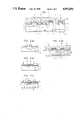
- FIG. 1is a sectional view illustrating one embodiment of the present invention
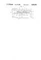
- FIGS. 2(a) to 2(d)are sectional views illustrating major steps for manufacturing the vertical field effect transistor of the one embodiment of the present invention.
- FIG. 3is a sectional view illustrating the motion of electrons and the expansion of the depletion layer when the field effect transistor shown in FIG. 1 is in operation.
- FIG. 1is a sectional view of a preferred embodiment in which the present invention is adapted to an n-channel insulated-gate vertical field effect transistor.
- an n + -type Sb doped silicon substrate 1having an impurity concentration of 3.0 ⁇ 10 18 atoms/cm 3
- an n - -type epitaxially grown layer 2having an impurity concentration of 6.4 ⁇ 10 14 atoms/cm 3 and a film thickness of 30 ⁇ m.
- a p - -type base region 3having a depth of 4 ⁇ m and an impurity concentration of 2.5 ⁇ 10 17 atoms/cm 3 is provided in the surface region of the n - -type epitaxially grown layer 2.
- n +-type source region 4having a depth of 1.0 ⁇ m and an impurity concentration of 2.0 ⁇ 10 20 atoms/ cm 3 is formed in a central surface portion of the p - -type base region 3.
- a p + -type region 7having an impurity concentration of 2.0 ⁇ 10 18 atoms/cm 3 from the surface thereof to reach the p - -type base region 3.
- an n + -type region 5having a depth of 2.0 ⁇ m and an impurity concentration of 1.0 ⁇ 10 15 atoms/cm 3
- a p + -type region 8having an impurity concentration of 2.0 ⁇ 10 18 atoms/cm 3 and a depth of 1.5 ⁇ m.
- a gate electrode 6 of polycrystalline siliconis formed on the p - -type base region 3 between the n + -type source region 4 and the n + -type region 5 through a gate insulating film.
- An, oxide film 29 having a thickness of 6000 ⁇is formed on the n + -type region 5 and on the p + -type region 8 between the gate electrodes 6.
- a source electrode 10is provided being commonly connected to the n + -type source region 4 and to the p + -type region 3, and a drain electrode 11 is provided on the back surface of the n + -type silicon substrate 1.
- an n - -type epitaxial layer 2is grown on the n-type semiconductor substrate 1, and p-type impurities are implanted by using an oxide film 9 as a mask to form a p - -type region 3.
- n-type impuritiesare implanted at a high concentration in order to form an n + -type source region 4.
- n-type impuritiesare implanted at a high concentration in the surface layer of the drain region 5 by using another oxide film 21 as a mask.
- p-type impuritiesare implanted at a high concentration using a polycrystalline silicon layer 6 as a mask in order to form p + -type layers 7 and 8.
- ionsare implanted and diffused to a suitable depth, followed by forming an oxide film 29 on the drain region, forming a source electrode 10 thereon, and forming a drain electrode 11 on the back surface of the substrate 1.
- FIG. 3shows a flow of electrons and the expansion of the depletion layer, when the insulated gate field effect transistor of this embodiment is in operation. Electrons flowing out from the n + -type source region 4 pass through the channel 12 and the surface layer of the drain region 5 to arrive at the drain electrode 11.
- the drain region 5is formed by implanting impurity ions at a high concentration after the p - -type region 3 has been formed.
- a relationship of dosageis p + -type layer 8 (5 ⁇ 10 14 /cm 2 to 5 ⁇ 10 16 /cm 2 ) > drain region 5 (2 ⁇ 10 11 /cm 2 to 5 ⁇ 10 14 /cm 2 ) > p - -type region 3. Due to the drive-in diffusion, therefore, the drain region 5 diffuses in the lateral direction toward the p - -type region 3 to shorten the channel 12. Moreover, since the surface of the drain region 5 has a high concentration, the on-resistance decreases.
- the p + -type layer 8 in the drain regionis under the floated condition, the depletion layer is expanded like the field ring, and concentration of electric field is relaxed under the gate electrode 6. Therefore, the breakdown voltage is prevented from decreasing.
Landscapes
- Insulated Gate Type Field-Effect Transistor (AREA)
- Junction Field-Effect Transistors (AREA)
Abstract
Description
1 Field of the Invention
The present invention relates to a field effect transistor, and more particularly, to improvements of breakdown voltage and on-resistance of a vertical field effect transistor.
2 Description of the Related Art
A conventional vertical field effect transistor is disclosed in Japanese Patent Laid-Open No. 53-135284 and U.S. Pat. No. 4,593,302 and has an n- -type active layer on an n+ -type substrate serving as a drain, a p-type base region formed in a surface area of the n- -type layer, an n+ -type source region formed in the p-type base region, a gate electrode positioned, through an insulating film, on the p-type base region between the n+ -type source region and the n- -type layer to extend over the n- -type layer, and an n+ -type layer formed in the surface area of the n- -type layer adjacent to the p-type base region. In such vertical field effect transistor, the electrons flowing from the n+ -type source region to the n+ -type drain region flow through a channel region induced at a surface of the p-type base region under the gate electrode. In this electron flow-path, since the n+ -type layer is formed on the surface of the n- -type layer adjacent to the p-type base region, the on-resistance of this field effect transistor decreases. With the n+ -type layer being provided on the surface of the n- -type in contact with the p-type base region, however, the breakdown voltage between the drain region and the base region decreases.
It is, therefore, an object of the present invention to provide a vertical field effect transistor which is so constructed as to decrease the on-resistance without lowering the breakdown voltage.
The field effect transistor in accordance with the present invention includes a first semiconductor region formed on a main surface of a semiconductor substrate of one conductivity type except for a predetermined portion of the substrate, the first semiconductor region being of the other conductivity type, a second semiconductor region formed on the main surface of the semiconductor substrate uncovered by the first semiconductor region, the second semiconductor region having the one conductivity type with an impurity concentration higher than the semiconductor substrate and being in contact with first semiconductor region, a third semiconductor region of the other conductivity type formed in the second semiconductor region, a fourth semiconductor region formed on a surface of the first semiconductor region, the fourth semiconductor region being separated from the second semiconductor region and being of the one conductivity type, a gate electrode formed on the first semiconductor region between the second semiconductor region and the fourth semiconductor region, an insulating film provided on the second semiconductor region and on the third semiconductor region, a first electrode electrically connected to the fourth semiconductor region and a second electrode electrically connected to the other main surface of the semiconductor substrate.
Since the second semiconductor region having the same conductivity type as the semiconductor substrate is formed on the main surface of the semiconductor substrate to have an impurity concentration higher than that of the semiconductor substrate, the field effect transistor according to the present invention has a small on-resistance. Furthermore, since the third semiconductor region of the other conductivity type is formed in the second semiconductor region together with the insulating film covering the second and third semiconductor regions, the third semiconductor region is under the floating condition to act just like a field ring to relax the concentration of electric field, resulting in keeping a high breakdown voltage. According to the present invention, therefore, there is obtained a field effect transistor having a decreased on-resistance with high breakdown voltage.
The third semiconductor region is preferably shallower than the second semiconductor region, because, if the third semiconductor region becomes deeper than the second semiconductor region, the current path becomes narrow to increase the on-resistance.
The above and further objects, features and advantages of the present invention will become more apparent from the following detailed description taken in conjunction with the accompanying drawings, wherein:
FIG. 1 is a sectional view illustrating one embodiment of the present invention;
FIGS. 2(a) to 2(d) are sectional views illustrating major steps for manufacturing the vertical field effect transistor of the one embodiment of the present invention; and
FIG. 3 is a sectional view illustrating the motion of electrons and the expansion of the depletion layer when the field effect transistor shown in FIG. 1 is in operation.
FIG. 1 is a sectional view of a preferred embodiment in which the present invention is adapted to an n-channel insulated-gate vertical field effect transistor. On an n+ -type Sb dopedsilicon substrate 1 having an impurity concentration of 3.0 × 10¹⁸ atoms/cm3, is formed an n- -type epitaxially grownlayer 2 having an impurity concentration of 6.4 × 10¹⁴ atoms/cm3 and a film thickness of 30 μm. A p- -type base region 3 having a depth of 4 μm and an impurity concentration of 2.5 × 10¹⁷ atoms/cm3 is provided in the surface region of the n- -type epitaxially grownlayer 2. An n+-type source region 4 having a depth of 1.0 μm and an impurity concentration of 2.0 × 10²⁰ atoms/ cm3 is formed in a central surface portion of the p- -type base region 3. At a central portion of the n+ -type source region 4, is provided a p+ -type region 7 having an impurity concentration of 2.0 × 10¹⁸ atoms/cm3 from the surface thereof to reach the p- -type base region 3. At a surface portion of the n- -type epitaxially grownlayer 2 which is adjacent to the p- -type base region 3, is provided an n+ -type region 5 having a depth of 2.0 μm and an impurity concentration of 1.0 × 10¹⁵ atoms/cm3, and, at the central portion of the n+ -type region 5, is provided a p+ -type region 8 having an impurity concentration of 2.0 × 10¹⁸ atoms/cm3 and a depth of 1.5 μm. Agate electrode 6 of polycrystalline silicon is formed on the p- -type base region 3 between the n+ -type source region 4 and the n+ -type region 5 through a gate insulating film. An,oxide film 29 having a thickness of 6000 Å is formed on the n+ -type region 5 and on the p+ -type region 8 between thegate electrodes 6. Asource electrode 10 is provided being commonly connected to the n+ -type source region 4 and to the p+ -type region 3, and adrain electrode 11 is provided on the back surface of the n+ -type silicon substrate 1.
A method for manufacturing the vertical field effect transistor will now be described in conjunction with FIGS. 2(a) to 2(d).
As shown in FIG. 2(a), first, an n- -typeepitaxial layer 2 is grown on the n-type semiconductor substrate 1, and p-type impurities are implanted by using anoxide film 9 as a mask to form a p- -type region 3. Next, using the same mask, n-type impurities are implanted at a high concentration in order to form an n+ -type source region 4.
Next, as shown in FIG. 2(b), n-type impurities are implanted at a high concentration in the surface layer of thedrain region 5 by using anotheroxide film 21 as a mask.
Referring to FIG. 2(c), p-type impurities are implanted at a high concentration using apolycrystalline silicon layer 6 as a mask in order to form p+ -type layers
Then, as shown in FIG. 2(d), ions are implanted and diffused to a suitable depth, followed by forming anoxide film 29 on the drain region, forming asource electrode 10 thereon, and forming adrain electrode 11 on the back surface of thesubstrate 1.
FIG. 3 shows a flow of electrons and the expansion of the depletion layer, when the insulated gate field effect transistor of this embodiment is in operation. Electrons flowing out from the n+ -type source region 4 pass through thechannel 12 and the surface layer of thedrain region 5 to arrive at thedrain electrode 11.
Thedrain region 5 is formed by implanting impurity ions at a high concentration after the p- -type region 3 has been formed. A relationship of dosage is p+ -type layer 8 (5 × 10¹⁴ /cm2 to 5 × 10¹⁶ /cm2) > drain region 5 (2 × 10¹¹ /cm2 to 5 × 10¹⁴ /cm2) > p- -type region 3. Due to the drive-in diffusion, therefore, thedrain region 5 diffuses in the lateral direction toward the p- -type region 3 to shorten thechannel 12. Moreover, since the surface of thedrain region 5 has a high concentration, the on-resistance decreases.
The p+ -type layer 8 in the drain region is under the floated condition, the depletion layer is expanded like the field ring, and concentration of electric field is relaxed under thegate electrode 6. Therefore, the breakdown voltage is prevented from decreasing.
Though the foregoing embodiment has dealt with the n-channel field effect transistor, the same effects are also obtained even with the p-channel field-effect transistor in which the types of conduction are reversed.
Claims (4)
1. A field effect transistor comprising:
a first semiconductor region formed on a main surface of a semiconductor substrate of one conductivity type except for a predetermined portion of said semiconductor substrate, said first semiconductor region being of the other conductivity type;
a second semiconductor region formed on said main surface of said semiconductor substrate uncovered by said first semiconductor region, said second semiconductor region having said one conductivity type with an impurity concentration higher than said semiconductor substrate;
a third semiconductor region of the other conductivity type formed in said second semiconductor region;
a fourth semiconductor region formed on a surface of said first semiconductor region, said fourth semiconductor region being separated from said second semiconductor region and said fourth semiconductor region being of said one conductivity type;
a gate electrode formed on said first semiconductor region between said second semiconductor region and said fourth semiconductor region;
an insulating film provided on said second semiconductor region and on said third semiconductor region;
a first electrode electrically connected to the fourth semiconductor region; and
a second electrode electrically connected to the other main surface of said semiconductor substrate.
2. A field effect transistor as claimed in claim 1, wherein said third semiconductor region is shallower than said second semiconductor region.
3. A vertical field effect transistor comprising:
a drain region of one conductivity type;
a base region of the other conductivity type provided on one main surface of said drain region;
a source region of said one conductivity type provided in said base region;
a first semiconductor region of said one conductivity type provided on said one main surface of said drain region between portions of said base region, said first semiconductor region having an impurity concentration higher than that of said drain region;
a second semiconductor region of the other conductivity type provided in said first semiconductor region;
a gate electrode provided on said base region between said source region and said first semiconductor region;
an insulating film provided on said second semiconductor region;
a source electrode electrically connected to said source region; and
a drain electrode electrically connected to said drain region.
4. A vertical field effect transistor as claimed in claim 3, wherein said second semiconductor region is shallower than said first semiconductor region.
Applications Claiming Priority (2)
| Application Number | Priority Date | Filing Date | Title |
|---|---|---|---|
| JP63-211858 | 1988-08-25 | ||
| JP63211858AJPH0783119B2 (en) | 1988-08-25 | 1988-08-25 | Field effect transistor |
Publications (1)
| Publication Number | Publication Date |
|---|---|
| US4952991Atrue US4952991A (en) | 1990-08-28 |
Family
ID=16612766
Family Applications (1)
| Application Number | Title | Priority Date | Filing Date |
|---|---|---|---|
| US07/397,232Expired - LifetimeUS4952991A (en) | 1988-08-25 | 1989-08-23 | Vertical field-effect transistor having a high breakdown voltage and a small on-resistance |
Country Status (3)
| Country | Link |
|---|---|
| US (1) | US4952991A (en) |
| EP (1) | EP0358389A1 (en) |
| JP (1) | JPH0783119B2 (en) |
Cited By (10)
| Publication number | Priority date | Publication date | Assignee | Title |
|---|---|---|---|---|
| US5072268A (en)* | 1991-03-12 | 1991-12-10 | Power Integrations, Inc. | MOS gated bipolar transistor |
| US5243234A (en)* | 1991-03-20 | 1993-09-07 | Industrial Technology Research Institute | Dual gate LDMOSFET device for reducing on state resistance |
| US5506421A (en)* | 1992-11-24 | 1996-04-09 | Cree Research, Inc. | Power MOSFET in silicon carbide |
| US5719421A (en)* | 1994-10-13 | 1998-02-17 | Texas Instruments Incorporated | DMOS transistor with low on-resistance and method of fabrication |
| US5719409A (en)* | 1996-06-06 | 1998-02-17 | Cree Research, Inc. | Silicon carbide metal-insulator semiconductor field effect transistor |
| US5750429A (en)* | 1995-10-23 | 1998-05-12 | Toyota Jidosha Kabushiki Kaisha | Semiconductor device and manufacture method of the same |
| US5777371A (en)* | 1995-09-29 | 1998-07-07 | Kabushiki Kaisha Toshiba | High-breakdown-voltage semiconductor device |
| US6617643B1 (en)* | 2002-06-28 | 2003-09-09 | Mcnc | Low power tunneling metal-oxide-semiconductor (MOS) device |
| US20120009741A1 (en)* | 2010-07-06 | 2012-01-12 | Shanghai Institute Of Microsystem And Information Technology, Chinese Academy | Soi mos device having a source/body ohmic contact and manufacturing method thereof |
| US20150069506A1 (en)* | 2013-09-11 | 2015-03-12 | Kabushiki Kaisha Toshiba | Semiconductor device and method of fabricating the same |
Families Citing this family (12)
| Publication number | Priority date | Publication date | Assignee | Title |
|---|---|---|---|---|
| US5243211A (en)* | 1991-11-25 | 1993-09-07 | Harris Corporation | Power fet with shielded channels |
| JP2689874B2 (en)* | 1993-12-17 | 1997-12-10 | 関西日本電気株式会社 | High voltage MOS transistor |
| DE69509494T2 (en)* | 1995-02-24 | 1999-10-07 | Consorzio Per La Ricerca Sulla Microelettronica Nel Mezzogiorno, Catania | Power device as an integrated structure in MOS technology and method for its production |
| US5798554A (en)* | 1995-02-24 | 1998-08-25 | Consorzio Per La Ricerca Sulla Microelettronica Nel Mezzogiorno | MOS-technology power device integrated structure and manufacturing process thereof |
| DE69531783T2 (en)* | 1995-10-09 | 2004-07-15 | Consorzio Per La Ricerca Sulla Microelettronica Nel Mezzogiorno - Corimme | Manufacturing process for power arrangement with protective ring |
| EP0772242B1 (en)* | 1995-10-30 | 2006-04-05 | STMicroelectronics S.r.l. | Single feature size MOS technology power device |
| EP0772241B1 (en)* | 1995-10-30 | 2004-06-09 | STMicroelectronics S.r.l. | High density MOS technology power device |
| EP0772244B1 (en)* | 1995-11-06 | 2000-03-22 | Consorzio per la Ricerca sulla Microelettronica nel Mezzogiorno | MOS technology power device with low output resistance and low capacity and related manufacturing process |
| US6228719B1 (en) | 1995-11-06 | 2001-05-08 | Stmicroelectronics S.R.L. | MOS technology power device with low output resistance and low capacitance, and related manufacturing process |
| DE69518653T2 (en)* | 1995-12-28 | 2001-04-19 | Consorzio Per La Ricerca Sulla Microelettronica Nel Mezzogiorno, Catania | MOS technology power arrangement in an integrated structure |
| US6147362A (en)* | 1997-03-17 | 2000-11-14 | Honeywell International Inc. | High performance display pixel for electronics displays |
| DE69839439D1 (en) | 1998-05-26 | 2008-06-19 | St Microelectronics Srl | MOS technology power arrangement with high integration density |
Citations (3)
| Publication number | Priority date | Publication date | Assignee | Title |
|---|---|---|---|---|
| JPS53135284A (en)* | 1977-04-30 | 1978-11-25 | Nec Corp | Production of field effect transistor |
| US4593302A (en)* | 1980-08-18 | 1986-06-03 | International Rectifier Corporation | Process for manufacture of high power MOSFET with laterally distributed high carrier density beneath the gate oxide |
| US4884113A (en)* | 1984-12-25 | 1989-11-28 | Kabushiki Kaisha Toshiba | Double-diffused, insulated-gate, field effect transistor |
Family Cites Families (5)
| Publication number | Priority date | Publication date | Assignee | Title |
|---|---|---|---|---|
| DE3346286A1 (en)* | 1982-12-21 | 1984-06-28 | International Rectifier Corp., Los Angeles, Calif. | High-power metal-oxide field-effect transistor semiconductor component |
| JPS59167066A (en)* | 1983-03-14 | 1984-09-20 | Nissan Motor Co Ltd | Vertical type metal oxide semiconductor field effect transistor |
| JPS60262468A (en)* | 1984-06-08 | 1985-12-25 | Matsushita Electric Ind Co Ltd | Mos type field-effect transistor |
| JPS6211275A (en)* | 1986-07-18 | 1987-01-20 | Hitachi Ltd | Semiconductor device |
| EP0279403A3 (en)* | 1987-02-16 | 1988-12-07 | Nec Corporation | Vertical mos field effect transistor having a high withstand voltage and a high switching speed |
- 1988
- 1988-08-25JPJP63211858Apatent/JPH0783119B2/ennot_activeExpired - Lifetime
- 1989
- 1989-08-23USUS07/397,232patent/US4952991A/ennot_activeExpired - Lifetime
- 1989-08-25EPEP89308664Apatent/EP0358389A1/ennot_activeWithdrawn
Patent Citations (4)
| Publication number | Priority date | Publication date | Assignee | Title |
|---|---|---|---|---|
| JPS53135284A (en)* | 1977-04-30 | 1978-11-25 | Nec Corp | Production of field effect transistor |
| US4593302A (en)* | 1980-08-18 | 1986-06-03 | International Rectifier Corporation | Process for manufacture of high power MOSFET with laterally distributed high carrier density beneath the gate oxide |
| US4593302B1 (en)* | 1980-08-18 | 1998-02-03 | Int Rectifier Corp | Process for manufacture of high power mosfet laterally distributed high carrier density beneath the gate oxide |
| US4884113A (en)* | 1984-12-25 | 1989-11-28 | Kabushiki Kaisha Toshiba | Double-diffused, insulated-gate, field effect transistor |
Cited By (14)
| Publication number | Priority date | Publication date | Assignee | Title |
|---|---|---|---|---|
| US5072268A (en)* | 1991-03-12 | 1991-12-10 | Power Integrations, Inc. | MOS gated bipolar transistor |
| US5243234A (en)* | 1991-03-20 | 1993-09-07 | Industrial Technology Research Institute | Dual gate LDMOSFET device for reducing on state resistance |
| US5506421A (en)* | 1992-11-24 | 1996-04-09 | Cree Research, Inc. | Power MOSFET in silicon carbide |
| US5719421A (en)* | 1994-10-13 | 1998-02-17 | Texas Instruments Incorporated | DMOS transistor with low on-resistance and method of fabrication |
| US5777371A (en)* | 1995-09-29 | 1998-07-07 | Kabushiki Kaisha Toshiba | High-breakdown-voltage semiconductor device |
| US5750429A (en)* | 1995-10-23 | 1998-05-12 | Toyota Jidosha Kabushiki Kaisha | Semiconductor device and manufacture method of the same |
| US6034398A (en)* | 1995-10-23 | 2000-03-07 | Toyota Jidosha Kabushiki Kaisha | Semiconductor device and manufacturing method of the same |
| US5719409A (en)* | 1996-06-06 | 1998-02-17 | Cree Research, Inc. | Silicon carbide metal-insulator semiconductor field effect transistor |
| US5831288A (en)* | 1996-06-06 | 1998-11-03 | Cree Research, Inc. | Silicon carbide metal-insulator semiconductor field effect transistor |
| US6617643B1 (en)* | 2002-06-28 | 2003-09-09 | Mcnc | Low power tunneling metal-oxide-semiconductor (MOS) device |
| US20120009741A1 (en)* | 2010-07-06 | 2012-01-12 | Shanghai Institute Of Microsystem And Information Technology, Chinese Academy | Soi mos device having a source/body ohmic contact and manufacturing method thereof |
| US8354310B2 (en)* | 2010-07-06 | 2013-01-15 | Shanghai Institute Of Microsystem And Information Technology, Chinese Academy Of Sciences | SOI MOS device having a source/body ohmic contact and manufacturing method thereof |
| US20150069506A1 (en)* | 2013-09-11 | 2015-03-12 | Kabushiki Kaisha Toshiba | Semiconductor device and method of fabricating the same |
| US9035381B2 (en)* | 2013-09-11 | 2015-05-19 | Kabushiki Kaisha Toshiba | Semiconductor device and method of fabricating the same |
Also Published As
| Publication number | Publication date |
|---|---|
| JPH0783119B2 (en) | 1995-09-06 |
| EP0358389A1 (en) | 1990-03-14 |
| JPH0260169A (en) | 1990-02-28 |
Similar Documents
| Publication | Publication Date | Title |
|---|---|---|
| US4952991A (en) | Vertical field-effect transistor having a high breakdown voltage and a small on-resistance | |
| US6713794B2 (en) | Lateral semiconductor device | |
| KR100232369B1 (en) | Enhanced performance lateral double-diffusion mos transistor and method of fabrication | |
| US6614089B2 (en) | Field effect transistor | |
| US5411901A (en) | Method of making high voltage transistor | |
| US6091086A (en) | Reverse blocking IGBT | |
| US7605040B2 (en) | Method of forming high breakdown voltage low on-resistance lateral DMOS transistor | |
| US5016066A (en) | Vertical power MOSFET having high withstand voltage and high switching speed | |
| US5801431A (en) | MOS gated semiconductor device with source metal covering the active gate | |
| US6933560B2 (en) | Power devices and methods for manufacturing the same | |
| US5382536A (en) | Method of fabricating lateral DMOS structure | |
| JPH0336311B2 (en) | ||
| US7074681B2 (en) | Semiconductor component and method of manufacturing | |
| US6030870A (en) | High density MOS technology power device | |
| JP2000077663A (en) | Field effect type semiconductor device | |
| JP2808871B2 (en) | Method for manufacturing MOS type semiconductor device | |
| JPH07226514A (en) | High conductivity insulated gate bipolar transistor integrated structure | |
| US4916500A (en) | MOS field effect transistor device with buried channel | |
| US5523601A (en) | High-breakdown-voltage MOS transistor | |
| US6107127A (en) | Method of making shallow well MOSFET structure | |
| US6727527B1 (en) | Reverse blocking IGBT | |
| US20040061170A1 (en) | Reverse blocking IGBT | |
| JP3223125B2 (en) | Semiconductor device and method of manufacturing semiconductor device | |
| JPH0644605B2 (en) | Method of manufacturing high breakdown voltage MOS field effect semiconductor device | |
| JP3233002B2 (en) | Field effect transistor |
Legal Events
| Date | Code | Title | Description |
|---|---|---|---|
| AS | Assignment | Owner name:NEC CORPORATION, JAPAN Free format text:ASSIGNMENT OF ASSIGNORS INTEREST.;ASSIGNOR:KAYAMA, CHIZURU;REEL/FRAME:005116/0515 Effective date:19890817 | |
| STCF | Information on status: patent grant | Free format text:PATENTED CASE | |
| FEPP | Fee payment procedure | Free format text:PAYOR NUMBER ASSIGNED (ORIGINAL EVENT CODE: ASPN); ENTITY STATUS OF PATENT OWNER: LARGE ENTITY | |
| FPAY | Fee payment | Year of fee payment:4 | |
| FEPP | Fee payment procedure | Free format text:PAYOR NUMBER ASSIGNED (ORIGINAL EVENT CODE: ASPN); ENTITY STATUS OF PATENT OWNER: LARGE ENTITY Free format text:PAYER NUMBER DE-ASSIGNED (ORIGINAL EVENT CODE: RMPN); ENTITY STATUS OF PATENT OWNER: LARGE ENTITY | |
| FPAY | Fee payment | Year of fee payment:8 | |
| FPAY | Fee payment | Year of fee payment:12 | |
| AS | Assignment | Owner name:NEC ELECTRONICS CORPORATION, JAPAN Free format text:ASSIGNMENT OF ASSIGNORS INTEREST;ASSIGNOR:NEC CORPORATION;REEL/FRAME:013758/0440 Effective date:20021101 |