US4948751A - Moelcular beam epitaxy for selective epitaxial growth of III - V compound semiconductor - Google Patents
Moelcular beam epitaxy for selective epitaxial growth of III - V compound semiconductorDownload PDFInfo
- Publication number
- US4948751A US4948751AUS07/196,009US19600988AUS4948751AUS 4948751 AUS4948751 AUS 4948751AUS 19600988 AUS19600988 AUS 19600988AUS 4948751 AUS4948751 AUS 4948751A
- Authority
- US
- United States
- Prior art keywords
- iii
- compound semiconductor
- substrate
- group iii
- semiconductor substrate
- Prior art date
- Legal status (The legal status is an assumption and is not a legal conclusion. Google has not performed a legal analysis and makes no representation as to the accuracy of the status listed.)
- Expired - Lifetime
Links
Images


Classifications
- H—ELECTRICITY
- H01—ELECTRIC ELEMENTS
- H01L—SEMICONDUCTOR DEVICES NOT COVERED BY CLASS H10
- H01L21/00—Processes or apparatus adapted for the manufacture or treatment of semiconductor or solid state devices or of parts thereof
- H01L21/02—Manufacture or treatment of semiconductor devices or of parts thereof
- H01L21/02104—Forming layers
- H01L21/02365—Forming inorganic semiconducting materials on a substrate
- H01L21/02367—Substrates
- H01L21/0237—Materials
- H01L21/02387—Group 13/15 materials
- H01L21/02395—Arsenides
- H—ELECTRICITY
- H01—ELECTRIC ELEMENTS
- H01L—SEMICONDUCTOR DEVICES NOT COVERED BY CLASS H10
- H01L21/00—Processes or apparatus adapted for the manufacture or treatment of semiconductor or solid state devices or of parts thereof
- H01L21/02—Manufacture or treatment of semiconductor devices or of parts thereof
- H01L21/02104—Forming layers
- H01L21/02365—Forming inorganic semiconducting materials on a substrate
- H01L21/02436—Intermediate layers between substrates and deposited layers
- H01L21/02439—Materials
- H01L21/02455—Group 13/15 materials
- H01L21/02463—Arsenides
- H—ELECTRICITY
- H01—ELECTRIC ELEMENTS
- H01L—SEMICONDUCTOR DEVICES NOT COVERED BY CLASS H10
- H01L21/00—Processes or apparatus adapted for the manufacture or treatment of semiconductor or solid state devices or of parts thereof
- H01L21/02—Manufacture or treatment of semiconductor devices or of parts thereof
- H01L21/02104—Forming layers
- H01L21/02365—Forming inorganic semiconducting materials on a substrate
- H01L21/02436—Intermediate layers between substrates and deposited layers
- H01L21/02439—Materials
- H01L21/02488—Insulating materials
- H—ELECTRICITY
- H01—ELECTRIC ELEMENTS
- H01L—SEMICONDUCTOR DEVICES NOT COVERED BY CLASS H10
- H01L21/00—Processes or apparatus adapted for the manufacture or treatment of semiconductor or solid state devices or of parts thereof
- H01L21/02—Manufacture or treatment of semiconductor devices or of parts thereof
- H01L21/02104—Forming layers
- H01L21/02365—Forming inorganic semiconducting materials on a substrate
- H01L21/02518—Deposited layers
- H01L21/02521—Materials
- H01L21/02538—Group 13/15 materials
- H01L21/02546—Arsenides
- H—ELECTRICITY
- H01—ELECTRIC ELEMENTS
- H01L—SEMICONDUCTOR DEVICES NOT COVERED BY CLASS H10
- H01L21/00—Processes or apparatus adapted for the manufacture or treatment of semiconductor or solid state devices or of parts thereof
- H01L21/02—Manufacture or treatment of semiconductor devices or of parts thereof
- H01L21/02104—Forming layers
- H01L21/02365—Forming inorganic semiconducting materials on a substrate
- H01L21/02612—Formation types
- H01L21/02617—Deposition types
- H01L21/02636—Selective deposition, e.g. simultaneous growth of mono- and non-monocrystalline semiconductor materials
- H01L21/02639—Preparation of substrate for selective deposition
- H—ELECTRICITY
- H01—ELECTRIC ELEMENTS
- H01L—SEMICONDUCTOR DEVICES NOT COVERED BY CLASS H10
- H01L21/00—Processes or apparatus adapted for the manufacture or treatment of semiconductor or solid state devices or of parts thereof
- H01L21/02—Manufacture or treatment of semiconductor devices or of parts thereof
- H01L21/02104—Forming layers
- H01L21/02365—Forming inorganic semiconducting materials on a substrate
- H01L21/02656—Special treatments
- H01L21/02658—Pretreatments
- H01L21/02661—In-situ cleaning
- Y—GENERAL TAGGING OF NEW TECHNOLOGICAL DEVELOPMENTS; GENERAL TAGGING OF CROSS-SECTIONAL TECHNOLOGIES SPANNING OVER SEVERAL SECTIONS OF THE IPC; TECHNICAL SUBJECTS COVERED BY FORMER USPC CROSS-REFERENCE ART COLLECTIONS [XRACs] AND DIGESTS
- Y10—TECHNICAL SUBJECTS COVERED BY FORMER USPC
- Y10S—TECHNICAL SUBJECTS COVERED BY FORMER USPC CROSS-REFERENCE ART COLLECTIONS [XRACs] AND DIGESTS
- Y10S148/00—Metal treatment
- Y10S148/026—Deposition thru hole in mask
- Y—GENERAL TAGGING OF NEW TECHNOLOGICAL DEVELOPMENTS; GENERAL TAGGING OF CROSS-SECTIONAL TECHNOLOGIES SPANNING OVER SEVERAL SECTIONS OF THE IPC; TECHNICAL SUBJECTS COVERED BY FORMER USPC CROSS-REFERENCE ART COLLECTIONS [XRACs] AND DIGESTS
- Y10—TECHNICAL SUBJECTS COVERED BY FORMER USPC
- Y10S—TECHNICAL SUBJECTS COVERED BY FORMER USPC CROSS-REFERENCE ART COLLECTIONS [XRACs] AND DIGESTS
- Y10S148/00—Metal treatment
- Y10S148/065—Gp III-V generic compounds-processing
- Y—GENERAL TAGGING OF NEW TECHNOLOGICAL DEVELOPMENTS; GENERAL TAGGING OF CROSS-SECTIONAL TECHNOLOGIES SPANNING OVER SEVERAL SECTIONS OF THE IPC; TECHNICAL SUBJECTS COVERED BY FORMER USPC CROSS-REFERENCE ART COLLECTIONS [XRACs] AND DIGESTS
- Y10—TECHNICAL SUBJECTS COVERED BY FORMER USPC
- Y10S—TECHNICAL SUBJECTS COVERED BY FORMER USPC CROSS-REFERENCE ART COLLECTIONS [XRACs] AND DIGESTS
- Y10S148/00—Metal treatment
- Y10S148/097—Lattice strain and defects
- Y—GENERAL TAGGING OF NEW TECHNOLOGICAL DEVELOPMENTS; GENERAL TAGGING OF CROSS-SECTIONAL TECHNOLOGIES SPANNING OVER SEVERAL SECTIONS OF THE IPC; TECHNICAL SUBJECTS COVERED BY FORMER USPC CROSS-REFERENCE ART COLLECTIONS [XRACs] AND DIGESTS
- Y10—TECHNICAL SUBJECTS COVERED BY FORMER USPC
- Y10S—TECHNICAL SUBJECTS COVERED BY FORMER USPC CROSS-REFERENCE ART COLLECTIONS [XRACs] AND DIGESTS
- Y10S148/00—Metal treatment
- Y10S148/169—Vacuum deposition, e.g. including molecular beam epitaxy
- Y—GENERAL TAGGING OF NEW TECHNOLOGICAL DEVELOPMENTS; GENERAL TAGGING OF CROSS-SECTIONAL TECHNOLOGIES SPANNING OVER SEVERAL SECTIONS OF THE IPC; TECHNICAL SUBJECTS COVERED BY FORMER USPC CROSS-REFERENCE ART COLLECTIONS [XRACs] AND DIGESTS
- Y10—TECHNICAL SUBJECTS COVERED BY FORMER USPC
- Y10S—TECHNICAL SUBJECTS COVERED BY FORMER USPC CROSS-REFERENCE ART COLLECTIONS [XRACs] AND DIGESTS
- Y10S438/00—Semiconductor device manufacturing: process
- Y10S438/909—Controlled atmosphere
Definitions
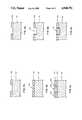
- FIG. 2(b)shows the result of the growth of InAs at the growth temperature of from 500° to 650° C. on the GaAs substrate 21 on which SiO 2 22 was formed selectively as shown in FIG. 2(a).
- InAs 23was formed only on the GaAs substrate 21, and was not deposited on SiO 2 22.
- Table 1illustrates the relation between the compound semiconductor materials grown on the semiconductor substrate and the substrate temperature.
- the partial pressure of the Group III elements supplied from the effusion cell for the Group III elementsis the quantity corresponding to the growth rate of 1.7 ⁇ m/hr and the partial pressure of the Group V elements is sufficiently greater than that of the Group III elements.
- SiO 2was used as the insulator film on the compound semiconductor substrate, the same result could be obtained by using silicon nitride instead of SiO 2 .
Landscapes
- Engineering & Computer Science (AREA)
- Physics & Mathematics (AREA)
- Condensed Matter Physics & Semiconductors (AREA)
- General Physics & Mathematics (AREA)
- Manufacturing & Machinery (AREA)
- Computer Hardware Design (AREA)
- Microelectronics & Electronic Packaging (AREA)
- Power Engineering (AREA)
- Chemical & Material Sciences (AREA)
- Materials Engineering (AREA)
- Physical Deposition Of Substances That Are Components Of Semiconductor Devices (AREA)
Abstract
Description
P - P.sub.eq.
TABLE 1 ______________________________________ Semiconductor Temperature Temperature Temperature Materials A (°C.) B (°C.) C (°C.) ______________________________________ InSb below 470 above 570 470-570 InP below 470 above 570 470-570 GaSb below 600 above 720 600-720 GaP below 650 above 720 650-720 ______________________________________ NOTE: Temperature A: temperature where growth occurs both on the semiconductor substrate and on the insulator film. B: temperature where deposition does not occur. C: temperature where selective growth occurs.
Claims (21)
Applications Claiming Priority (2)
| Application Number | Priority Date | Filing Date | Title |
|---|---|---|---|
| JP62-124801 | 1987-05-20 | ||
| JP12480187 | 1987-05-20 |
Publications (1)
| Publication Number | Publication Date |
|---|---|
| US4948751Atrue US4948751A (en) | 1990-08-14 |
Family
ID=14894462
Family Applications (1)
| Application Number | Title | Priority Date | Filing Date |
|---|---|---|---|
| US07/196,009Expired - LifetimeUS4948751A (en) | 1987-05-20 | 1988-05-19 | Moelcular beam epitaxy for selective epitaxial growth of III - V compound semiconductor |
Country Status (2)
| Country | Link |
|---|---|
| US (1) | US4948751A (en) |
| JP (1) | JP2743377B2 (en) |
Cited By (13)
| Publication number | Priority date | Publication date | Assignee | Title |
|---|---|---|---|---|
| US5100830A (en)* | 1989-02-22 | 1992-03-31 | Kabushiki Kaisha Toshiba | Method of manufacturing a semiconductor device |
| US5192701A (en)* | 1988-03-17 | 1993-03-09 | Kabushiki Kaisha Toshiba | Method of manufacturing field effect transistors having different threshold voltages |
| US5250462A (en)* | 1990-08-24 | 1993-10-05 | Nec Corporation | Method for fabricating an optical semiconductor device |
| US5258327A (en)* | 1992-04-30 | 1993-11-02 | Litton Systems, Inc. | MBE growth method for high level devices and integrations |
| US5371038A (en)* | 1993-10-21 | 1994-12-06 | Motorola, Inc. | Method of forming a quantum multi-function semiconductor device |
| US5384282A (en)* | 1990-10-29 | 1995-01-24 | Mitsubishi Denki Kabushiki Kaisha | Method for producing an embedded optoelectronic integrated circuit |
| US5436181A (en)* | 1994-04-18 | 1995-07-25 | Texas Instruments Incorporated | Method of self aligning an emitter contact in a heterojunction bipolar transistor |
| EP0758144A1 (en)* | 1995-08-07 | 1997-02-12 | Motorola, Inc. | Semiconductor device and method of fabrication |
| US5677538A (en)* | 1995-07-07 | 1997-10-14 | Trustees Of Boston University | Photodetectors using III-V nitrides |
| EP0703605A3 (en)* | 1994-09-02 | 1998-03-11 | Mitsubishi Denki Kabushiki Kaisha | Method for etching semiconductor, method for fabricating semiconductor device, method for fabricating semiconductor laser, and semiconductor laser |
| US6139483A (en)* | 1993-07-27 | 2000-10-31 | Texas Instruments Incorporated | Method of forming lateral resonant tunneling devices |
| US20040147053A1 (en)* | 2002-09-30 | 2004-07-29 | Bookham Technology, Plc | Method for integrating optical devices in a single epitaxial growth step |
| US9263264B2 (en) | 2011-03-14 | 2016-02-16 | University Of Leeds | Oxide removal from semiconductor surfaces using a flux of indium atoms |
Citations (10)
| Publication number | Priority date | Publication date | Assignee | Title |
|---|---|---|---|---|
| US3751310A (en)* | 1971-03-25 | 1973-08-07 | Bell Telephone Labor Inc | Germanium doped epitaxial films by the molecular beam method |
| US3928092A (en)* | 1974-08-28 | 1975-12-23 | Bell Telephone Labor Inc | Simultaneous molecular beam deposition of monocrystalline and polycrystalline III(a)-V(a) compounds to produce semiconductor devices |
| US4111725A (en)* | 1977-05-06 | 1978-09-05 | Bell Telephone Laboratories, Incorporated | Selective lift-off technique for fabricating gaas fets |
| JPS54138382A (en)* | 1978-04-20 | 1979-10-26 | Fujitsu Ltd | Manufacture for semiconductor integrated circuit device |
| US4181544A (en)* | 1976-12-30 | 1980-01-01 | Bell Telephone Laboratories, Incorporated | Molecular beam method for processing a plurality of substrates |
| JPS6066810A (en)* | 1983-09-24 | 1985-04-17 | Agency Of Ind Science & Technol | Molecular beam epitaxy growth method |
| US4517047A (en)* | 1981-01-23 | 1985-05-14 | The United States Of America As Represented By The Secretary Of The Army | MBE growth technique for matching superlattices grown on GaAs substrates |
| US4622093A (en)* | 1983-07-27 | 1986-11-11 | At&T Bell Laboratories | Method of selective area epitaxial growth using ion beams |
| US4622083A (en)* | 1985-03-11 | 1986-11-11 | Texas Instruments Incorporated | Molecular beam epitaxial process |
| US4637129A (en)* | 1984-07-30 | 1987-01-20 | At&T Bell Laboratories | Selective area III-V growth and lift-off using tungsten patterning |
Family Cites Families (3)
| Publication number | Priority date | Publication date | Assignee | Title |
|---|---|---|---|---|
| JPS5096179A (en)* | 1973-12-24 | 1975-07-31 | ||
| JPS52143761A (en)* | 1976-05-26 | 1977-11-30 | Hitachi Ltd | Crystal growth method |
| JPS551164A (en)* | 1979-02-08 | 1980-01-07 | Matsushita Electric Ind Co Ltd | Method of fabricating semiconductor laser device |
- 1988
- 1988-04-28JPJP63108637Apatent/JP2743377B2/ennot_activeExpired - Lifetime
- 1988-05-19USUS07/196,009patent/US4948751A/ennot_activeExpired - Lifetime
Patent Citations (10)
| Publication number | Priority date | Publication date | Assignee | Title |
|---|---|---|---|---|
| US3751310A (en)* | 1971-03-25 | 1973-08-07 | Bell Telephone Labor Inc | Germanium doped epitaxial films by the molecular beam method |
| US3928092A (en)* | 1974-08-28 | 1975-12-23 | Bell Telephone Labor Inc | Simultaneous molecular beam deposition of monocrystalline and polycrystalline III(a)-V(a) compounds to produce semiconductor devices |
| US4181544A (en)* | 1976-12-30 | 1980-01-01 | Bell Telephone Laboratories, Incorporated | Molecular beam method for processing a plurality of substrates |
| US4111725A (en)* | 1977-05-06 | 1978-09-05 | Bell Telephone Laboratories, Incorporated | Selective lift-off technique for fabricating gaas fets |
| JPS54138382A (en)* | 1978-04-20 | 1979-10-26 | Fujitsu Ltd | Manufacture for semiconductor integrated circuit device |
| US4517047A (en)* | 1981-01-23 | 1985-05-14 | The United States Of America As Represented By The Secretary Of The Army | MBE growth technique for matching superlattices grown on GaAs substrates |
| US4622093A (en)* | 1983-07-27 | 1986-11-11 | At&T Bell Laboratories | Method of selective area epitaxial growth using ion beams |
| JPS6066810A (en)* | 1983-09-24 | 1985-04-17 | Agency Of Ind Science & Technol | Molecular beam epitaxy growth method |
| US4637129A (en)* | 1984-07-30 | 1987-01-20 | At&T Bell Laboratories | Selective area III-V growth and lift-off using tungsten patterning |
| US4622083A (en)* | 1985-03-11 | 1986-11-11 | Texas Instruments Incorporated | Molecular beam epitaxial process |
Non-Patent Citations (12)
| Title |
|---|
| "Applied Physics Letters", vol. 48 (1986), pp. 142-144. |
| "Journal of Applied Physics", vol. 46 (1975), pp. 783-785. |
| "Journal of Applied Physics", vol. 55 (1985), pp. 3163-3165. |
| "Journal of Crystal Growth", vol. 77, (1986), pp. 303-309. |
| "Journal of Electrochemical Society", vol. 127 (1980), pp. 1562-1567. |
| Applied Physics Letters , vol. 48 (1986), pp. 142 144.* |
| Journal of Applied Physics , vol. 46 (1975), pp. 783 785.* |
| Journal of Applied Physics , vol. 55 (1985), pp. 3163 3165.* |
| Journal of Crystal Growth , vol. 77, (1986), pp. 303 309.* |
| Journal of Electrochemical Society , vol. 127 (1980), pp. 1562 1567.* |
| Li et al., "Aspects of GaAs Selective Area Growth by Molecular Beam Epitaxy . . .", J. Electrochem. Soc., vol. 130, No. 10, Oct. 1983, pp. 2072-5. |
| Li et al., Aspects of GaAs Selective Area Growth by Molecular Beam Epitaxy . . . , J. Electrochem. Soc., vol. 130, No. 10, Oct. 1983, pp. 2072 5.* |
Cited By (16)
| Publication number | Priority date | Publication date | Assignee | Title |
|---|---|---|---|---|
| US5192701A (en)* | 1988-03-17 | 1993-03-09 | Kabushiki Kaisha Toshiba | Method of manufacturing field effect transistors having different threshold voltages |
| US5100830A (en)* | 1989-02-22 | 1992-03-31 | Kabushiki Kaisha Toshiba | Method of manufacturing a semiconductor device |
| US5250462A (en)* | 1990-08-24 | 1993-10-05 | Nec Corporation | Method for fabricating an optical semiconductor device |
| US5384282A (en)* | 1990-10-29 | 1995-01-24 | Mitsubishi Denki Kabushiki Kaisha | Method for producing an embedded optoelectronic integrated circuit |
| US5258327A (en)* | 1992-04-30 | 1993-11-02 | Litton Systems, Inc. | MBE growth method for high level devices and integrations |
| US6139483A (en)* | 1993-07-27 | 2000-10-31 | Texas Instruments Incorporated | Method of forming lateral resonant tunneling devices |
| US5371038A (en)* | 1993-10-21 | 1994-12-06 | Motorola, Inc. | Method of forming a quantum multi-function semiconductor device |
| US5548141A (en)* | 1994-04-18 | 1996-08-20 | Texas Instruments Incorporated | Bipolar transistor having a self emitter contact aligned |
| US5436181A (en)* | 1994-04-18 | 1995-07-25 | Texas Instruments Incorporated | Method of self aligning an emitter contact in a heterojunction bipolar transistor |
| EP0703605A3 (en)* | 1994-09-02 | 1998-03-11 | Mitsubishi Denki Kabushiki Kaisha | Method for etching semiconductor, method for fabricating semiconductor device, method for fabricating semiconductor laser, and semiconductor laser |
| US5872022A (en)* | 1994-09-02 | 1999-02-16 | Mitsubishi Denki Kabushiki Kaisha | Method for etching a semiconductor method for fabricating semiconductor device method for fabricating semiconductor laser and semiconductor laser |
| US5677538A (en)* | 1995-07-07 | 1997-10-14 | Trustees Of Boston University | Photodetectors using III-V nitrides |
| EP0758144A1 (en)* | 1995-08-07 | 1997-02-12 | Motorola, Inc. | Semiconductor device and method of fabrication |
| US20040147053A1 (en)* | 2002-09-30 | 2004-07-29 | Bookham Technology, Plc | Method for integrating optical devices in a single epitaxial growth step |
| US7060516B2 (en)* | 2002-09-30 | 2006-06-13 | Bookham Technology, Plc | Method for integrating optical devices in a single epitaxial growth step |
| US9263264B2 (en) | 2011-03-14 | 2016-02-16 | University Of Leeds | Oxide removal from semiconductor surfaces using a flux of indium atoms |
Also Published As
| Publication number | Publication date |
|---|---|
| JPS6453411A (en) | 1989-03-01 |
| JP2743377B2 (en) | 1998-04-22 |
Similar Documents
| Publication | Publication Date | Title |
|---|---|---|
| US3915765A (en) | MBE technique for fabricating semiconductor devices having low series resistance | |
| EP0576566B1 (en) | A method for the preparation and doping of highly insulating monocrystalline gallium nitride thin films | |
| US3751310A (en) | Germanium doped epitaxial films by the molecular beam method | |
| US4559091A (en) | Method for producing hyperabrupt doping profiles in semiconductors | |
| CA1225571A (en) | Growth of oriented single crystal semiconductor on insulator | |
| US4960728A (en) | Homogenization anneal of II-VI compounds | |
| US4948751A (en) | Moelcular beam epitaxy for selective epitaxial growth of III - V compound semiconductor | |
| Hovel et al. | The Epitaxy of ZnSe on Ge, GaAs, and ZnSe by an HCl Close‐Spaced Transport Process | |
| JPH0383332A (en) | Manufacture of silicon carbide semiconductor device | |
| US6030453A (en) | III-V epitaxial wafer production | |
| JPS6329928A (en) | Method of making gallium arsenite grow on silicon by epitaxial growth | |
| JPH06140346A (en) | Manufacture of heteroepitaxial thin layer and of electronic device | |
| JPH10289906A5 (en) | ||
| EP1038056B1 (en) | A method of growing a buffer layer using molecular beam epitaxy | |
| US4470192A (en) | Method of selected area doping of compound semiconductors | |
| Chang et al. | Effect of growth temperature on epitaxial lateral overgrowth of GaAs on Si substrate | |
| US4421576A (en) | Method for forming an epitaxial compound semiconductor layer on a semi-insulating substrate | |
| EP0524817B1 (en) | Crystal growth method of III - V compound semiconductor | |
| US5548136A (en) | Substrate with a compound semiconductor surface layer and method for preparing the same | |
| US4246050A (en) | Lattice constant grading in the Aly Ca1-y As1-x Sbx alloy system | |
| US5653802A (en) | Method for forming crystal | |
| US5142350A (en) | Transistor having cubic boron nitride layer | |
| US5232862A (en) | Method of fabricating a transistor having a cubic boron nitride layer | |
| US4426237A (en) | Volatile metal oxide suppression in molecular beam epitaxy systems | |
| US4089714A (en) | Doping mercury cadmium telluride with aluminum or silicon |
Legal Events
| Date | Code | Title | Description |
|---|---|---|---|
| AS | Assignment | Owner name:NEC CORPORATION, 33-1, SHIBA 5-CHOME, MINATO-KU, T Free format text:ASSIGNMENT OF ASSIGNORS INTEREST.;ASSIGNORS:OKAMOTO, AKIHIKO;OHATA, KEIICHI;REEL/FRAME:004945/0456 Effective date:19880519 Owner name:NEC CORPORATION, JAPAN Free format text:ASSIGNMENT OF ASSIGNORS INTEREST;ASSIGNORS:OKAMOTO, AKIHIKO;OHATA, KEIICHI;REEL/FRAME:004945/0456 Effective date:19880519 | |
| STCF | Information on status: patent grant | Free format text:PATENTED CASE | |
| FEPP | Fee payment procedure | Free format text:PAYOR NUMBER ASSIGNED (ORIGINAL EVENT CODE: ASPN); ENTITY STATUS OF PATENT OWNER: LARGE ENTITY | |
| FPAY | Fee payment | Year of fee payment:4 | |
| FEPP | Fee payment procedure | Free format text:PAYER NUMBER DE-ASSIGNED (ORIGINAL EVENT CODE: RMPN); ENTITY STATUS OF PATENT OWNER: LARGE ENTITY Free format text:PAYOR NUMBER ASSIGNED (ORIGINAL EVENT CODE: ASPN); ENTITY STATUS OF PATENT OWNER: LARGE ENTITY | |
| FPAY | Fee payment | Year of fee payment:8 | |
| FPAY | Fee payment | Year of fee payment:12 |