US4943346A - Method for manufacturing printed circuit boards - Google Patents
Method for manufacturing printed circuit boardsDownload PDFInfo
- Publication number
- US4943346A US4943346AUS07/401,834US40183489AUS4943346AUS 4943346 AUS4943346 AUS 4943346AUS 40183489 AUS40183489 AUS 40183489AUS 4943346 AUS4943346 AUS 4943346A
- Authority
- US
- United States
- Prior art keywords
- etch resist
- metal layer
- resist layer
- printed circuit
- circuit boards
- Prior art date
- Legal status (The legal status is an assumption and is not a legal conclusion. Google has not performed a legal analysis and makes no representation as to the accuracy of the status listed.)
- Expired - Fee Related
Links
- 238000000034methodMethods0.000titleclaimsabstractdescription35
- 238000004519manufacturing processMethods0.000titleclaimsabstractdescription25
- 239000002184metalSubstances0.000claimsabstractdescription58
- 229910052751metalInorganic materials0.000claimsabstractdescription58
- 239000000758substrateSubstances0.000claimsabstractdescription32
- 238000005530etchingMethods0.000claimsabstractdescription13
- ATJFFYVFTNAWJD-UHFFFAOYSA-NTinChemical compound[Sn]ATJFFYVFTNAWJD-UHFFFAOYSA-N0.000claimsabstractdescription8
- 230000005670electromagnetic radiationEffects0.000claimsdescription7
- 238000000151depositionMethods0.000claimsdescription6
- RYGMFSIKBFXOCR-UHFFFAOYSA-NCopperChemical compound[Cu]RYGMFSIKBFXOCR-UHFFFAOYSA-N0.000claimsdescription5
- 229910052802copperInorganic materials0.000claimsdescription5
- 239000010949copperSubstances0.000claimsdescription5
- 230000008021depositionEffects0.000claimsdescription5
- 239000008151electrolyte solutionSubstances0.000claimsdescription5
- 238000004090dissolutionMethods0.000claimsdescription4
- 238000010186stainingMethods0.000claimsdescription4
- 238000004140cleaningMethods0.000claimsdescription3
- 229910001174tin-lead alloyInorganic materials0.000claimsdescription3
- 239000004922lacquerSubstances0.000claimsdescription2
- 229910000679solderInorganic materials0.000claimsdescription2
- 238000005496temperingMethods0.000claimsdescription2
- 150000002894organic compoundsChemical class0.000claims2
- 238000005476solderingMethods0.000abstractdescription2
- 239000000463materialSubstances0.000description4
- 238000001465metallisationMethods0.000description4
- 230000006911nucleationEffects0.000description4
- 238000010899nucleationMethods0.000description4
- 238000012986modificationMethods0.000description3
- 230000004048modificationEffects0.000description3
- 230000008901benefitEffects0.000description2
- 238000007796conventional methodMethods0.000description2
- 238000005538encapsulationMethods0.000description2
- 238000005516engineering processMethods0.000description2
- 239000000126substanceSubstances0.000description2
- 239000004697PolyetherimideSubstances0.000description1
- 229910021626Tin(II) chlorideInorganic materials0.000description1
- RPJKYODNJDVOOO-UHFFFAOYSA-N[B].FChemical compound[B].FRPJKYODNJDVOOO-UHFFFAOYSA-N0.000description1
- 239000000654additiveSubstances0.000description1
- 230000000996additive effectEffects0.000description1
- 230000009286beneficial effectEffects0.000description1
- 230000015572biosynthetic processEffects0.000description1
- 239000011152fibreglassSubstances0.000description1
- 238000007654immersionMethods0.000description1
- 238000002347injectionMethods0.000description1
- 239000007924injectionSubstances0.000description1
- 238000001746injection mouldingMethods0.000description1
- 238000002955isolationMethods0.000description1
- 238000007747platingMethods0.000description1
- 229920001601polyetherimidePolymers0.000description1
- 230000005855radiationEffects0.000description1
- 238000002910structure generationMethods0.000description1
- 229920001169thermoplasticPolymers0.000description1
- 239000004416thermosoftening plasticSubstances0.000description1
Images

Classifications
- B—PERFORMING OPERATIONS; TRANSPORTING
- B44—DECORATIVE ARTS
- B44C—PRODUCING DECORATIVE EFFECTS; MOSAICS; TARSIA WORK; PAPERHANGING
- B44C1/00—Processes, not specifically provided for elsewhere, for producing decorative surface effects
- B44C1/22—Removing surface-material, e.g. by engraving, by etching
- C—CHEMISTRY; METALLURGY
- C23—COATING METALLIC MATERIAL; COATING MATERIAL WITH METALLIC MATERIAL; CHEMICAL SURFACE TREATMENT; DIFFUSION TREATMENT OF METALLIC MATERIAL; COATING BY VACUUM EVAPORATION, BY SPUTTERING, BY ION IMPLANTATION OR BY CHEMICAL VAPOUR DEPOSITION, IN GENERAL; INHIBITING CORROSION OF METALLIC MATERIAL OR INCRUSTATION IN GENERAL
- C23F—NON-MECHANICAL REMOVAL OF METALLIC MATERIAL FROM SURFACE; INHIBITING CORROSION OF METALLIC MATERIAL OR INCRUSTATION IN GENERAL; MULTI-STEP PROCESSES FOR SURFACE TREATMENT OF METALLIC MATERIAL INVOLVING AT LEAST ONE PROCESS PROVIDED FOR IN CLASS C23 AND AT LEAST ONE PROCESS COVERED BY SUBCLASS C21D OR C22F OR CLASS C25
- C23F1/00—Etching metallic material by chemical means
- C23F1/02—Local etching
- H—ELECTRICITY
- H05—ELECTRIC TECHNIQUES NOT OTHERWISE PROVIDED FOR
- H05K—PRINTED CIRCUITS; CASINGS OR CONSTRUCTIONAL DETAILS OF ELECTRIC APPARATUS; MANUFACTURE OF ASSEMBLAGES OF ELECTRICAL COMPONENTS
- H05K3/00—Apparatus or processes for manufacturing printed circuits
- H05K3/02—Apparatus or processes for manufacturing printed circuits in which the conductive material is applied to the surface of the insulating support and is thereafter removed from such areas of the surface which are not intended for current conducting or shielding
- H05K3/06—Apparatus or processes for manufacturing printed circuits in which the conductive material is applied to the surface of the insulating support and is thereafter removed from such areas of the surface which are not intended for current conducting or shielding the conductive material being removed chemically or electrolytically, e.g. by photo-etch process
- H05K3/061—Etching masks
- H05K3/062—Etching masks consisting of metals or alloys or metallic inorganic compounds
- H—ELECTRICITY
- H05—ELECTRIC TECHNIQUES NOT OTHERWISE PROVIDED FOR
- H05K—PRINTED CIRCUITS; CASINGS OR CONSTRUCTIONAL DETAILS OF ELECTRIC APPARATUS; MANUFACTURE OF ASSEMBLAGES OF ELECTRICAL COMPONENTS
- H05K3/00—Apparatus or processes for manufacturing printed circuits
- H05K3/02—Apparatus or processes for manufacturing printed circuits in which the conductive material is applied to the surface of the insulating support and is thereafter removed from such areas of the surface which are not intended for current conducting or shielding
- H05K3/06—Apparatus or processes for manufacturing printed circuits in which the conductive material is applied to the surface of the insulating support and is thereafter removed from such areas of the surface which are not intended for current conducting or shielding the conductive material being removed chemically or electrolytically, e.g. by photo-etch process
- H05K3/07—Apparatus or processes for manufacturing printed circuits in which the conductive material is applied to the surface of the insulating support and is thereafter removed from such areas of the surface which are not intended for current conducting or shielding the conductive material being removed chemically or electrolytically, e.g. by photo-etch process being removed electrolytically
- B—PERFORMING OPERATIONS; TRANSPORTING
- B29—WORKING OF PLASTICS; WORKING OF SUBSTANCES IN A PLASTIC STATE IN GENERAL
- B29L—INDEXING SCHEME ASSOCIATED WITH SUBCLASS B29C, RELATING TO PARTICULAR ARTICLES
- B29L2031/00—Other particular articles
- B29L2031/34—Electrical apparatus, e.g. sparking plugs or parts thereof
- B29L2031/3493—Moulded interconnect devices, i.e. moulded articles provided with integrated circuit traces
- H—ELECTRICITY
- H05—ELECTRIC TECHNIQUES NOT OTHERWISE PROVIDED FOR
- H05K—PRINTED CIRCUITS; CASINGS OR CONSTRUCTIONAL DETAILS OF ELECTRIC APPARATUS; MANUFACTURE OF ASSEMBLAGES OF ELECTRICAL COMPONENTS
- H05K2201/00—Indexing scheme relating to printed circuits covered by H05K1/00
- H05K2201/03—Conductive materials
- H05K2201/0302—Properties and characteristics in general
- H05K2201/0305—Solder used for other purposes than connections between PCB or components, e.g. for filling vias or for programmable patterns
- H—ELECTRICITY
- H05—ELECTRIC TECHNIQUES NOT OTHERWISE PROVIDED FOR
- H05K—PRINTED CIRCUITS; CASINGS OR CONSTRUCTIONAL DETAILS OF ELECTRIC APPARATUS; MANUFACTURE OF ASSEMBLAGES OF ELECTRICAL COMPONENTS
- H05K2201/00—Indexing scheme relating to printed circuits covered by H05K1/00
- H05K2201/09—Shape and layout
- H05K2201/09009—Substrate related
- H05K2201/09118—Moulded substrate
- H—ELECTRICITY
- H05—ELECTRIC TECHNIQUES NOT OTHERWISE PROVIDED FOR
- H05K—PRINTED CIRCUITS; CASINGS OR CONSTRUCTIONAL DETAILS OF ELECTRIC APPARATUS; MANUFACTURE OF ASSEMBLAGES OF ELECTRICAL COMPONENTS
- H05K2201/00—Indexing scheme relating to printed circuits covered by H05K1/00
- H05K2201/09—Shape and layout
- H05K2201/09209—Shape and layout details of conductors
- H05K2201/0929—Conductive planes
- H05K2201/09363—Conductive planes wherein only contours around conductors are removed for insulation
- H—ELECTRICITY
- H05—ELECTRIC TECHNIQUES NOT OTHERWISE PROVIDED FOR
- H05K—PRINTED CIRCUITS; CASINGS OR CONSTRUCTIONAL DETAILS OF ELECTRIC APPARATUS; MANUFACTURE OF ASSEMBLAGES OF ELECTRICAL COMPONENTS
- H05K2203/00—Indexing scheme relating to apparatus or processes for manufacturing printed circuits covered by H05K3/00
- H05K2203/03—Metal processing
- H05K2203/0361—Stripping a part of an upper metal layer to expose a lower metal layer, e.g. by etching or using a laser
- H—ELECTRICITY
- H05—ELECTRIC TECHNIQUES NOT OTHERWISE PROVIDED FOR
- H05K—PRINTED CIRCUITS; CASINGS OR CONSTRUCTIONAL DETAILS OF ELECTRIC APPARATUS; MANUFACTURE OF ASSEMBLAGES OF ELECTRICAL COMPONENTS
- H05K2203/00—Indexing scheme relating to apparatus or processes for manufacturing printed circuits covered by H05K3/00
- H05K2203/07—Treatments involving liquids, e.g. plating, rinsing
- H05K2203/0703—Plating
- H05K2203/072—Electroless plating, e.g. finish plating or initial plating
- H—ELECTRICITY
- H05—ELECTRIC TECHNIQUES NOT OTHERWISE PROVIDED FOR
- H05K—PRINTED CIRCUITS; CASINGS OR CONSTRUCTIONAL DETAILS OF ELECTRIC APPARATUS; MANUFACTURE OF ASSEMBLAGES OF ELECTRICAL COMPONENTS
- H05K2203/00—Indexing scheme relating to apparatus or processes for manufacturing printed circuits covered by H05K3/00
- H05K2203/13—Moulding and encapsulation; Deposition techniques; Protective layers
- H05K2203/1333—Deposition techniques, e.g. coating
- H05K2203/135—Electrophoretic deposition of insulating material
- H—ELECTRICITY
- H05—ELECTRIC TECHNIQUES NOT OTHERWISE PROVIDED FOR
- H05K—PRINTED CIRCUITS; CASINGS OR CONSTRUCTIONAL DETAILS OF ELECTRIC APPARATUS; MANUFACTURE OF ASSEMBLAGES OF ELECTRICAL COMPONENTS
- H05K2203/00—Indexing scheme relating to apparatus or processes for manufacturing printed circuits covered by H05K3/00
- H05K2203/14—Related to the order of processing steps
- H05K2203/1476—Same or similar kind of process performed in phases, e.g. coarse patterning followed by fine patterning
- H—ELECTRICITY
- H05—ELECTRIC TECHNIQUES NOT OTHERWISE PROVIDED FOR
- H05K—PRINTED CIRCUITS; CASINGS OR CONSTRUCTIONAL DETAILS OF ELECTRIC APPARATUS; MANUFACTURE OF ASSEMBLAGES OF ELECTRICAL COMPONENTS
- H05K3/00—Apparatus or processes for manufacturing printed circuits
- H05K3/0011—Working of insulating substrates or insulating layers
- H05K3/0017—Etching of the substrate by chemical or physical means
- H05K3/0026—Etching of the substrate by chemical or physical means by laser ablation
- H05K3/0032—Etching of the substrate by chemical or physical means by laser ablation of organic insulating material
- H—ELECTRICITY
- H05—ELECTRIC TECHNIQUES NOT OTHERWISE PROVIDED FOR
- H05K—PRINTED CIRCUITS; CASINGS OR CONSTRUCTIONAL DETAILS OF ELECTRIC APPARATUS; MANUFACTURE OF ASSEMBLAGES OF ELECTRICAL COMPONENTS
- H05K3/00—Apparatus or processes for manufacturing printed circuits
- H05K3/02—Apparatus or processes for manufacturing printed circuits in which the conductive material is applied to the surface of the insulating support and is thereafter removed from such areas of the surface which are not intended for current conducting or shielding
- H05K3/027—Apparatus or processes for manufacturing printed circuits in which the conductive material is applied to the surface of the insulating support and is thereafter removed from such areas of the surface which are not intended for current conducting or shielding the conductive material being removed by irradiation, e.g. by photons, alpha or beta particles
- Y—GENERAL TAGGING OF NEW TECHNOLOGICAL DEVELOPMENTS; GENERAL TAGGING OF CROSS-SECTIONAL TECHNOLOGIES SPANNING OVER SEVERAL SECTIONS OF THE IPC; TECHNICAL SUBJECTS COVERED BY FORMER USPC CROSS-REFERENCE ART COLLECTIONS [XRACs] AND DIGESTS
- Y10—TECHNICAL SUBJECTS COVERED BY FORMER USPC
- Y10T—TECHNICAL SUBJECTS COVERED BY FORMER US CLASSIFICATION
- Y10T29/00—Metal working
- Y10T29/49—Method of mechanical manufacture
- Y10T29/49002—Electrical device making
- Y10T29/49117—Conductor or circuit manufacturing
- Y10T29/49124—On flat or curved insulated base, e.g., printed circuit, etc.
- Y10T29/49155—Manufacturing circuit on or in base
- Y10T29/49165—Manufacturing circuit on or in base by forming conductive walled aperture in base
Definitions
- the inventionrelates to a method for manufacturing printed circuit boards using integrated circuit fabrication technology.
- an etch resist layeris applied onto a metal layer. This resist layer is then selectively removed to form a resist pattern so that the metal layer can be selectively etched. The etch resist layer is then completely removed to leave an interconnection pattern.
- the selective removal of the etch resist layercan be accomplished using a scan method with a laser. However, this conventional method is involved and time-consuming. This is particularly true when the interconnects lie relatively far apart and large surfaces of the etch resist layer must be removed.
- An object of the present inventionis to provide an improved method for manufacturing printed circuit boards so that the selective removal of the etch resist layer with electromagnetic radiation can be executed quickly and with little expense.
- a metal layer and a first etch resist layerare successively applied onto an electrically insulating substrate.
- the first etch resist layeris then selectively removed with electromagnetic radiation in those regions over the areas of the metal layer that will be etched.
- the areas of the metal layer exposed from selective removal of the etch resist layerare etched away down to the surface of the substrate.
- the first etch resist layeris then completely removed.
- a second metallic etch resist layeris applied onto the remaining regions of the metal layer. Some of the remaining regions do not correspond to the interconnect pattern that is desired. These regions are connected to the anode of a voltage source.
- the etch resist over the anodically contacted regionsis electrolytically removed. The regions of the metal layer exposed are etched away down to the surface of the substrate.
- the method of the inventionhas only the regions of the first etch resist layer that are adjacent and above the regions of the metal layer to be etched are removed with electromagnetic radiation.
- the formation of the first etch resist pattern, using electromagnetic radiation,can be quickly executed due to the small area of first etch resist layer to be eroded.
- the undesired regions of the metal layerremain between the interconnects.
- the second etch resist layeris formed on all regions of the metal layer.
- the undesired regionscan be anodically contacted with little effort and expense after the interconnects (desired regions of the metal layer) are encapsulated with a second etch resist layer.
- the second etch resist layer on the undesired regionis removed.
- the encapsulation of the interconnects with etch resistis preserved, so that only the undesired regions of the metal layer between the interconnects will be etched away.
- a major advantage of the method of the present inventionis total isolation of the interconnects on the substrate.
- the interconnectsrepresent islands that are not anodically contacted. Conversely, all undesired metal surfaces must be electrically connected to one another. This connection is easily achieved by a corresponding design of the interconnect patterns, clamps, contact bridges or the like.
- the first etch resist layeris completely removed before the application of the second etch resist layer.
- the metal layeris applied onto the substrate by currentless and voltaic deposition of copper.
- This type of metal layer depositionis particularly advantageous when manufacturing interconnects having through-contacts.
- Metallization of the corresponding through-contact holescan also be formed by the currentless and voltaic deposition of copper.
- etch resist layerscan be structured with a laser so they guarantee reliable protection of the metal interconnection layer lying therebelow during etching.
- the first etch resist layer and the second etch resist layerare preferably applied by currentless metal deposition. This can be implemented in an especially economical fashion to provide reliable protection of the metal layer to be used as interconnects.
- the electromagnetic radiationis preferably generated by a laser which is well suited for the removal of etch resist layers.
- the movement of the laser beam relative to the substrateshould be freely programmable.
- the desired design of the interconnect patterncan be quickly implemented while maintaining modification capabilities.
- the method of the inventionprovides similar economic benefits when a three-dimension, injection molded substrate having injected through-contact holes is employed. Such substrates can be fabricated in great numbers at low cost by injection molding. The three-dimensional design of the substrates or printed circuit boards does not present any problem in structure generation with electromagnetic radiation.
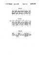
- FIGS. 1 through 10show highly simplified, cross-sectional views of the printed circuit board during the various steps in the manufacturing method according to the principles of the present invention.
- the substrate 1 illustrated in FIG. 1involves a portion of a base material having injected through-contact holes 2.
- High-temperature-resistant thermoplasticssuch as fiberglass or reinforced polyetherimide, are particularly suitable as materials for the substrate of printed circuit boards manufactured according to the method of the present invention.
- the substrate 1 shown in FIG. 1was cleaned and stained to improve the adhesion of the interconnects and through-contactings thereto.
- Commercially available bathswere employed for both the staining and the cleaning of the substrate 1.
- the staining bathis specifically adapted to the particular substrate material.
- nucleation 3was applied onto the surface of the substrate 1 and onto the walls of the through-contact holes 2.
- the application of the nucleation 3is accomplished by immersing the substrate 1 into a PcCl 2 -SnCl 2 bath.
- commercially available baths based on palladium-organic compoundshave also proven suitable for the application of the nucleation 3.
- the nucleation 3After the application of the nucleation 3, it is activated to realize a reduced in thickness. Such a step is standard in additive technology.
- An extremely thin layerwas subsequently applied according to FIG. 3 by chemical metal deposition which is free of external current.
- the base layer that is applied in a commercially available currentless copper bathcoats the surfaces of the substrate 1 and the walls of the through-contacting holes 2.
- a metal layer 4is formed with a thickness of, for example, 30 micrometers.
- a first etch resist layer 5is then applied onto metal layer 4 by currentless metal deposition, this etch resist layer 5 may be composed of tin as in the preferred embodiment.
- the first etch resist layer 5is then structured by a scan method with the assistance of a Nd-YAG laser. Radiation from the laser is indicated by arrows S. The selective removal of the etch resist layer 5 is limited to the region 6 that is over the areas of the metal layer that will be etched.
- the regions of the metal layer 4 exposedare to be removed by etching, using standard etching techniques.
- FIG. 6shows that the interconnect pattern appears after this etching step.
- the undesired regions 8 of the metal layer 4still remain between the desired regions 4 or interconnects.
- a second metallic etch resist layer 7that is similarly composed of tin, as in the preferred embodiment, is applied onto the regions of the metal layer 4 and metal layer 8, according to FIG. 8.
- the second etch resist layeralso protects the sides of walls of the interconnects. According to FIG. 9, all undesired regions 8 between the interconnects are subsequently anodically contacted. This anodic contact is indicated by a plus sign.
- the second etch resist layer 7 in the undesired regions 8is electrolytically dissolved in a suitable anodically contacted. This anodic contact is indicated by a plus sign.
- the second etch resist layer 7 in the undesired regions 8is electrolytically dissolved in a suitable electrolyte solution of, for example, boron-hydrogen fluoride.
- the regions of the etch resist layer 7 on the interconnectsare not dissolved.
- the exposed, undesired regions 8 of the metal layer 4can be etched away down to the surface of the substrate 1. According to FIG. 10, only the regions of the metal layer 4 on the substrate surfaces and in the through-contact holes 2 that correspond to the interconnect pattern will remain on the substrate 1 after etching. Since the second etch resist layer 7 remaining on the interconnect pattern is composed of tin, it need not be removed. Component soldering is improved by the tin present in the region of the through-contacts 2. Tempering at a temperature of, for example, 130°, can then be performed.
- the application of a solder stop lacquer with subsequent hot-tinning of the remaining regions of the metal 4can also be performed.
- the remaining second etch resist layer 7could also be removed by stripping, preferably executed in a chemical way, as in the removal of the first etch resist layer 5.
- the etch resist layer 5, that is applied onto the metal layer 4,may be organic.
- An organic etch resist that can be electrophoretically appliedis preferred. Such a deposition can be performed by electro immersion backering.
- a resist material, EAGLE, distributed by the Shiplay Company,is suitable.
- the pattern of the etch resist layeris again formed by a laser scan method, as indicated by the arrows S in FIG. 5.
Landscapes
- Engineering & Computer Science (AREA)
- Chemical & Material Sciences (AREA)
- Manufacturing & Machinery (AREA)
- Microelectronics & Electronic Packaging (AREA)
- Metallurgy (AREA)
- Chemical Kinetics & Catalysis (AREA)
- General Chemical & Material Sciences (AREA)
- Materials Engineering (AREA)
- Mechanical Engineering (AREA)
- Organic Chemistry (AREA)
- Manufacturing Of Printed Circuit Boards (AREA)
- ing And Chemical Polishing (AREA)
Abstract
Description
1. Field of the Invention
The invention relates to a method for manufacturing printed circuit boards using integrated circuit fabrication technology.
2. Description of the Prior Art
In standard printed circuit board manufacturing, an etch resist layer is applied onto a metal layer. This resist layer is then selectively removed to form a resist pattern so that the metal layer can be selectively etched. The etch resist layer is then completely removed to leave an interconnection pattern. Such a process is disclosed in EP-A-No. 0 062,300. The selective removal of the etch resist layer can be accomplished using a scan method with a laser. However, this conventional method is involved and time-consuming. This is particularly true when the interconnects lie relatively far apart and large surfaces of the etch resist layer must be removed.
An object of the present invention is to provide an improved method for manufacturing printed circuit boards so that the selective removal of the etch resist layer with electromagnetic radiation can be executed quickly and with little expense.
The above object is achieved in a method executed in accordance with the principles of the present invention. First, a metal layer and a first etch resist layer are successively applied onto an electrically insulating substrate. The first etch resist layer is then selectively removed with electromagnetic radiation in those regions over the areas of the metal layer that will be etched. The areas of the metal layer exposed from selective removal of the etch resist layer are etched away down to the surface of the substrate. The first etch resist layer is then completely removed. A second metallic etch resist layer is applied onto the remaining regions of the metal layer. Some of the remaining regions do not correspond to the interconnect pattern that is desired. These regions are connected to the anode of a voltage source. Next, the etch resist over the anodically contacted regions is electrolytically removed. The regions of the metal layer exposed are etched away down to the surface of the substrate.
Differing from conventional methods, the method of the invention has only the regions of the first etch resist layer that are adjacent and above the regions of the metal layer to be etched are removed with electromagnetic radiation. The formation of the first etch resist pattern, using electromagnetic radiation, can be quickly executed due to the small area of first etch resist layer to be eroded. After the etching then, however, the undesired regions of the metal layer remain between the interconnects. The second etch resist layer is formed on all regions of the metal layer. The undesired regions can be anodically contacted with little effort and expense after the interconnects (desired regions of the metal layer) are encapsulated with a second etch resist layer. The second etch resist layer on the undesired region is removed. The encapsulation of the interconnects with etch resist is preserved, so that only the undesired regions of the metal layer between the interconnects will be etched away.
A major advantage of the method of the present invention is total isolation of the interconnects on the substrate. The interconnects represent islands that are not anodically contacted. Conversely, all undesired metal surfaces must be electrically connected to one another. This connection is easily achieved by a corresponding design of the interconnect patterns, clamps, contact bridges or the like.
In a preferred embodiment of the method of the invention, after the metal layer is etched down to the substrate, the first etch resist layer is completely removed before the application of the second etch resist layer. This allows for the second resist layer to encapsulate the desired regions of the metal layer or interconnects. Such encapsulation guarantees the protection of the interconnects during the etching of the undesired regions of the metal layer.
In another embodiment of the method of the invention, the metal layer is applied onto the substrate by currentless and voltaic deposition of copper. This type of metal layer deposition is particularly advantageous when manufacturing interconnects having through-contacts. Metallization of the corresponding through-contact holes can also be formed by the currentless and voltaic deposition of copper.
It has also proven especially beneficial when tin or a tin-lead alloy is employed for the first and second etch resist layers. These etch resist layers can be structured with a laser so they guarantee reliable protection of the metal interconnection layer lying therebelow during etching.
The first etch resist layer and the second etch resist layer are preferably applied by currentless metal deposition. This can be implemented in an especially economical fashion to provide reliable protection of the metal layer to be used as interconnects.
The electromagnetic radiation is preferably generated by a laser which is well suited for the removal of etch resist layers. The movement of the laser beam relative to the substrate should be freely programmable. The desired design of the interconnect pattern can be quickly implemented while maintaining modification capabilities.
The method of the invention provides similar economic benefits when a three-dimension, injection molded substrate having injected through-contact holes is employed. Such substrates can be fabricated in great numbers at low cost by injection molding. The three-dimensional design of the substrates or printed circuit boards does not present any problem in structure generation with electromagnetic radiation.
FIGS. 1 through 10 show highly simplified, cross-sectional views of the printed circuit board during the various steps in the manufacturing method according to the principles of the present invention.
Thesubstrate 1 illustrated in FIG. 1 involves a portion of a base material having injected through-contact holes 2. High-temperature-resistant thermoplastics, such as fiberglass or reinforced polyetherimide, are particularly suitable as materials for the substrate of printed circuit boards manufactured according to the method of the present invention.
Thesubstrate 1 shown in FIG. 1 was cleaned and stained to improve the adhesion of the interconnects and through-contactings thereto. Commercially available baths were employed for both the staining and the cleaning of thesubstrate 1. The staining bath is specifically adapted to the particular substrate material.
After the staining and cleaning of thesubstrate 1, it is nucleated to yield a thin layer 3 as in FIG. 2. It is seen that the nucleation 3 was applied onto the surface of thesubstrate 1 and onto the walls of the through-contact holes 2. The application of the nucleation 3 is accomplished by immersing thesubstrate 1 into a PcCl2 -SnCl2 bath. However, commercially available baths based on palladium-organic compounds have also proven suitable for the application of the nucleation 3.
After the application of the nucleation 3, it is activated to realize a reduced in thickness. Such a step is standard in additive technology. An extremely thin layer was subsequently applied according to FIG. 3 by chemical metal deposition which is free of external current. The base layer that is applied in a commercially available currentless copper bath coats the surfaces of thesubstrate 1 and the walls of the through-contactingholes 2.
Copper-plating is then performed on the entire surface in currentless fashion and is also voltaically reinforced with copper. As a result, ametal layer 4 is formed with a thickness of, for example, 30 micrometers.
According to FIG. 4, a first etch resistlayer 5 is then applied ontometal layer 4 by currentless metal deposition, this etch resistlayer 5 may be composed of tin as in the preferred embodiment.
According to FIG. 5, the first etch resistlayer 5 is then structured by a scan method with the assistance of a Nd-YAG laser. Radiation from the laser is indicated by arrows S. The selective removal of the etch resistlayer 5 is limited to theregion 6 that is over the areas of the metal layer that will be etched.
After the selective removal of the first etch resistlayer 5, the regions of themetal layer 4 exposed are to be removed by etching, using standard etching techniques. FIG. 6 shows that the interconnect pattern appears after this etching step. Theundesired regions 8 of themetal layer 4 still remain between the desiredregions 4 or interconnects.
After stripping the first etch resistlayer 5 off the metal layer in FIG. 7 by dissolution in an electrolyte solution, a second metallic etch resistlayer 7 that is similarly composed of tin, as in the preferred embodiment, is applied onto the regions of themetal layer 4 andmetal layer 8, according to FIG. 8. The second etch resist layer also protects the sides of walls of the interconnects. According to FIG. 9, allundesired regions 8 between the interconnects are subsequently anodically contacted. This anodic contact is indicated by a plus sign. As in FIG. 9, the second etch resistlayer 7 in theundesired regions 8 is electrolytically dissolved in a suitable anodically contacted. This anodic contact is indicated by a plus sign. As in FIG. 9, the second etch resistlayer 7 in theundesired regions 8 is electrolytically dissolved in a suitable electrolyte solution of, for example, boron-hydrogen fluoride.
In the selective removal of the second etch resistlayer 7 set forth above, the regions of the etch resistlayer 7 on the interconnects are not dissolved. In the next etching step, the exposed,undesired regions 8 of themetal layer 4 can be etched away down to the surface of thesubstrate 1. According to FIG. 10, only the regions of themetal layer 4 on the substrate surfaces and in the through-contact holes 2 that correspond to the interconnect pattern will remain on thesubstrate 1 after etching. Since the second etch resistlayer 7 remaining on the interconnect pattern is composed of tin, it need not be removed. Component soldering is improved by the tin present in the region of the through-contacts 2. Tempering at a temperature of, for example, 130°, can then be performed. The application of a solder stop lacquer with subsequent hot-tinning of the remaining regions of themetal 4 can also be performed. As required, the remaining second etch resistlayer 7 could also be removed by stripping, preferably executed in a chemical way, as in the removal of the first etch resistlayer 5.
In another embodiment of the method set forth above, the etch resistlayer 5, that is applied onto themetal layer 4, may be organic. An organic etch resist that can be electrophoretically applied is preferred. Such a deposition can be performed by electro immersion backering. A resist material, EAGLE, distributed by the Shiplay Company, is suitable. The pattern of the etch resist layer is again formed by a laser scan method, as indicated by the arrows S in FIG. 5.
Although modifications and changes may be suggested by those skilled in the art, it is the invention of the inventor to embody within the patent warranted hereon, all changes and modifications as reasonably and properly come within his contribution to the art.
Claims (17)
1. A method for manufacturing printed circuit boards, comprising the steps of:
generating a metal layer on an insulating substrate;
applying a first etch resist layer onto said metal layer;
selectively removing said etch resist layer so as to expose a first undesired region of said metal layer;
completely etching said first undesired region away leaving a second undesired region of said metal layer and a desired region of said metal layer;
applying a second etch resist layer onto said second undesired region and said desired region of said metal layer;
selectively removing said second etch resist layer from said second undesired region of said metal layer;
anodically contacting said second undesired region of said metal layer; and
completely electrolytically etching said second undesired region away so as to leave said desired region of said metal layer remaining.
2. A method for manufacturing printed circuit board as claimed in claim 1, further comprising the steps of:
staining said insulating substrate so that adhesion of said metal layer to said insulating substrate is improved;
cleaning said substrate; and
nucleating said insulating substrate so as to form a thin layer thereon.
3. A method for manufacturing printed circuit boards as claimed in claim 1, further comprising the step of:
completely removing said first etch resist layer.
4. A method for manufacturing printed circuit boards, as claimed in claim 1, further comprising the step of:
removing said second etch resist layer from said desired regions of said metal layer.
5. A method for manufacturing printed circuit boards, as claimed in claim 1, further comprising the steps of:
tempering said insulating substrate and said desired regions of said metal layer; and
applying a solder stop lacquer onto said insulating substrate and said desired regions of said metal layer.
6. A method for manufacturing printed circuit boards, as claimed in claim 1, wherein the step of generating a metal layer is further defined by: depositing a metal layer of copper.
7. A method for manufacturing printed circuit boards, as claimed in claim 1, wherein the step of generating a metal layer is further defined by:
generating a metal layer by currentless and voltaic deposition.
8. A method for manufacturing printed circuit boards, as claimed in claim 1, wherein the step of applying a first etch resist layer is further defined by:
applying a first etch resist layer of tin or a tin-lead alloy.
9. A method for manufacturing printed circuit boards, as claimed in claim 1, wherein the step of applying a second etch resist layer is further defined by:
applying a second etch resist layer of tin or a tin lead alloy.
10. A method for manufacturing printed circuit boards, as claimed in claim 1, wherein the step of applying a first etch resist layer is further defined by:
applying a first etch resist layer of an organic compound.
11. A method for manufacturing printed circuit boards, as claimed in claim 1, wherein the step of applying an etch resist layer is further defined by:
applying a second etch resist layer of an organic compound.
12. A method for manufacturing printed circuit boards, as claimed in claim 1, wherein the step of applying a second etch resist layer is further defined by:
applying a second etch resist layer onto a top surface and side walls of said second undesired region and said desired region of said metal layer.
13. A method for manufacturing printed circuit boards, as claimed in claim 1, wherein the step of selectively removing said first etch resist layer is further defined by:
selectively removing said first etch resist layer by electromagnetic radiation generated by a laser whose movement is freely programmable.
14. A method for manufacturing printed circuit boards as claimed in claim 3, wherein the step of completely removing said first etch resist layer is further defined by:
completely removing said first etch resist layer by dissolution in an electrolyte solution.
15. A method for manufacturing printed circuit boards, as claimed in claim 1, wherein the step of selectively removing said second etch resist layer is further defined by:
selectively removing said second etch resist layer by dissolution in an electrolyte solution.
16. A method for manufacturing printed circuit boards, as claimed in claim 5, wherein the step of removing said second etch layer is further defined by:
removing said second etch layer by dissolution in an electrolyte solution.
17. A method for manufacturing printed circuit boards, as claimed in claim 1, wherein the step of generating a metal layer is further defined by:
generating a metal layer onto an insulating substrate having through-holes with inner walls, said inner walls are processed in the same fashion as said substrate.
Applications Claiming Priority (2)
| Application Number | Priority Date | Filing Date | Title |
|---|---|---|---|
| DE3833094 | 1988-09-29 | ||
| DE3833094 | 1988-09-29 |
Publications (1)
| Publication Number | Publication Date |
|---|---|
| US4943346Atrue US4943346A (en) | 1990-07-24 |
Family
ID=6363987
Family Applications (1)
| Application Number | Title | Priority Date | Filing Date |
|---|---|---|---|
| US07/401,834Expired - Fee RelatedUS4943346A (en) | 1988-09-29 | 1989-09-01 | Method for manufacturing printed circuit boards |
Country Status (4)
| Country | Link |
|---|---|
| US (1) | US4943346A (en) |
| EP (3) | EP0361192B1 (en) |
| JP (1) | JPH02128492A (en) |
| DE (1) | DE58907030D1 (en) |
Cited By (65)
| Publication number | Priority date | Publication date | Assignee | Title |
|---|---|---|---|---|
| WO1991018489A1 (en)* | 1990-05-16 | 1991-11-28 | Olin Corporation | Gtab manufacturing process and the product produced thereby |
| US5178726A (en)* | 1991-03-07 | 1993-01-12 | Minnesota Mining And Manufacturing Company | Process for producing a patterned metal surface |
| US5188702A (en)* | 1989-12-19 | 1993-02-23 | Nitto Denko Corporation | Process for producing an anisotropic conductive film |
| EP0530564A1 (en)* | 1991-09-05 | 1993-03-10 | Siemens Aktiengesellschaft | Method for producing circuit boards |
| US5417800A (en)* | 1992-02-19 | 1995-05-23 | Fujitsu Limited | Thin film circuit board manufacturing process |
| EP0679372A3 (en)* | 1994-04-25 | 1996-01-17 | Advanced Cardiovascular System | Radiopaque stent markers. |
| US5525205A (en)* | 1993-08-26 | 1996-06-11 | Polyplastics Co., Ltd. | Process for forming circuit with laser |
| US5603721A (en)* | 1991-10-28 | 1997-02-18 | Advanced Cardiovascular Systems, Inc. | Expandable stents and method for making same |
| US5651899A (en)* | 1994-02-01 | 1997-07-29 | Dyconex Patente Ag | Structuring of printed circuit boards |
| US5666722A (en)* | 1994-04-14 | 1997-09-16 | Hewlett-Packard Company | Method of manufacturing printed circuit boards |
| US5759416A (en)* | 1995-11-24 | 1998-06-02 | U.S. Philips Corporation | Method of selectively removing a metallic layer from a non-metallic substrate |
| US5868950A (en)* | 1996-11-08 | 1999-02-09 | W. L. Gore & Associates, Inc. | Method to correct astigmatism of fourth yag to enable formation of sub 25 micron micro-vias using masking techniques |
| US5879568A (en)* | 1996-06-18 | 1999-03-09 | Hitachi, Ltd. | Process for producing multilayer printed circuit board for wire bonding |
| US5985128A (en)* | 1997-01-22 | 1999-11-16 | International Business Machines Corporation | Method of performing processes on features with electricity |
| US6117104A (en)* | 1998-09-08 | 2000-09-12 | Advanced Cardiovascular Systems, Inc. | Stent deployment system and method of use |
| US6171334B1 (en) | 1998-06-17 | 2001-01-09 | Advanced Cardiovascular Systems, Inc. | Expandable stent and method of use |
| US6174329B1 (en) | 1996-08-22 | 2001-01-16 | Advanced Cardiovascular Systems, Inc. | Protective coating for a stent with intermediate radiopaque coating |
| US6355058B1 (en) | 1999-12-30 | 2002-03-12 | Advanced Cardiovascular Systems, Inc. | Stent with radiopaque coating consisting of particles in a binder |
| US6436132B1 (en) | 2000-03-30 | 2002-08-20 | Advanced Cardiovascular Systems, Inc. | Composite intraluminal prostheses |
| US6461380B1 (en) | 1998-07-28 | 2002-10-08 | Advanced Cardiovascular Systems, Inc. | Stent configuration |
| US6464723B1 (en) | 1999-04-22 | 2002-10-15 | Advanced Cardiovascular Systems, Inc. | Radiopaque stents |
| US6471721B1 (en) | 1999-12-30 | 2002-10-29 | Advanced Cardiovascular Systems, Inc. | Vascular stent having increased radiopacity and method for making same |
| US6485999B1 (en) | 1998-07-10 | 2002-11-26 | Siemens Aktiengesellschaft | Wiring arrangements having electrically conductive cross connections and method for producing same |
| US6537311B1 (en) | 1999-12-30 | 2003-03-25 | Advanced Cardiovascular Systems, Inc. | Stent designs for use in peripheral vessels |
| US6540774B1 (en) | 1999-08-31 | 2003-04-01 | Advanced Cardiovascular Systems, Inc. | Stent design with end rings having enhanced strength and radiopacity |
| US6585757B1 (en) | 1999-09-15 | 2003-07-01 | Advanced Cardiovascular Systems, Inc. | Endovascular stent with radiopaque spine |
| US6602287B1 (en) | 1999-12-08 | 2003-08-05 | Advanced Cardiovascular Systems, Inc. | Stent with anti-thrombogenic coating |
| US6605114B1 (en) | 1997-04-24 | 2003-08-12 | Advanced Cardiovascular Systems, Inc. | Heparin delivery method |
| US6652579B1 (en) | 2000-06-22 | 2003-11-25 | Advanced Cardiovascular Systems, Inc. | Radiopaque stent |
| US6662443B2 (en) | 1999-03-24 | 2003-12-16 | Fujitsu Limited | Method of fabricating a substrate with a via connection |
| US20040069636A1 (en)* | 2001-03-07 | 2004-04-15 | Heinrich Meyer | Metal pattern formation |
| US6739048B2 (en) | 1998-01-08 | 2004-05-25 | International Business Machines Corporation | Process of fabricating a circuitized structure |
| US6875229B2 (en) | 1997-08-13 | 2005-04-05 | Advanced Cardiovascular Systems, Inc. | Stent and catheter assembly and method for treating bifurcations |
| US6896697B1 (en) | 2002-12-30 | 2005-05-24 | Advanced Cardiovascular Systems, Inc. | Intravascular stent |
| US6899729B1 (en) | 2002-12-18 | 2005-05-31 | Advanced Cardiovascular Systems, Inc. | Stent for treating vulnerable plaque |
| US7163715B1 (en) | 2001-06-12 | 2007-01-16 | Advanced Cardiovascular Systems, Inc. | Spray processing of porous medical devices |
| US7198675B2 (en) | 2003-09-30 | 2007-04-03 | Advanced Cardiovascular Systems | Stent mandrel fixture and method for selectively coating surfaces of a stent |
| US7258697B1 (en) | 2003-12-22 | 2007-08-21 | Advanced Cardiovascular Systems, Inc. | Stent with anchors to prevent vulnerable plaque rupture during deployment |
| US7258891B2 (en) | 2001-06-28 | 2007-08-21 | Advanced Cardiovascular Systems, Inc. | Stent mounting assembly and a method of using the same to coat a stent |
| US7297159B2 (en) | 2000-10-26 | 2007-11-20 | Advanced Cardiovascular Systems, Inc. | Selective coating of medical devices |
| US7316710B1 (en) | 2002-12-30 | 2008-01-08 | Advanced Cardiovascular Systems, Inc. | Flexible stent |
| US7553377B1 (en) | 2004-04-27 | 2009-06-30 | Advanced Cardiovascular Systems, Inc. | Apparatus and method for electrostatic coating of an abluminal stent surface |
| US7563324B1 (en) | 2003-12-29 | 2009-07-21 | Advanced Cardiovascular Systems Inc. | System and method for coating an implantable medical device |
| US7632307B2 (en) | 2004-12-16 | 2009-12-15 | Advanced Cardiovascular Systems, Inc. | Abluminal, multilayer coating constructs for drug-delivery stents |
| US7753950B2 (en) | 1997-08-13 | 2010-07-13 | Advanced Cardiovascular Systems, Inc. | Stent and catheter assembly and method for treating bifurcations |
| US7763198B2 (en) | 2005-04-12 | 2010-07-27 | Abbott Cardiovascular Systems Inc. | Method for retaining a vascular stent on a catheter |
| US7867547B2 (en) | 2005-12-19 | 2011-01-11 | Advanced Cardiovascular Systems, Inc. | Selectively coating luminal surfaces of stents |
| US20110094103A1 (en)* | 2009-10-22 | 2011-04-28 | Silverbrook Research Pty Ltd | Method of fabricating inkjet printhed having low-loss contact for thermal actuators |
| US7947207B2 (en) | 2005-04-12 | 2011-05-24 | Abbott Cardiovascular Systems Inc. | Method for retaining a vascular stent on a catheter |
| US8003156B2 (en) | 2006-05-04 | 2011-08-23 | Advanced Cardiovascular Systems, Inc. | Rotatable support elements for stents |
| US8017237B2 (en) | 2006-06-23 | 2011-09-13 | Abbott Cardiovascular Systems, Inc. | Nanoshells on polymers |
| US8048441B2 (en) | 2007-06-25 | 2011-11-01 | Abbott Cardiovascular Systems, Inc. | Nanobead releasing medical devices |
| US8048448B2 (en) | 2006-06-15 | 2011-11-01 | Abbott Cardiovascular Systems Inc. | Nanoshells for drug delivery |
| US20110290663A1 (en)* | 2010-05-25 | 2011-12-01 | General Electric Company | System and method for metal cutting |
| US8216209B2 (en) | 2007-05-31 | 2012-07-10 | Abbott Cardiovascular Systems Inc. | Method and apparatus for delivering an agent to a kidney |
| US8603530B2 (en) | 2006-06-14 | 2013-12-10 | Abbott Cardiovascular Systems Inc. | Nanoshell therapy |
| US9144509B2 (en) | 2007-05-31 | 2015-09-29 | Abbott Cardiovascular Systems Inc. | Method and apparatus for delivering an agent to a kidney |
| US9149610B2 (en) | 2007-05-31 | 2015-10-06 | Abbott Cardiovascular Systems Inc. | Method and apparatus for improving delivery of an agent to a kidney |
| US9364586B2 (en) | 2007-05-31 | 2016-06-14 | Abbott Cardiovascular Systems Inc. | Method and apparatus for improving delivery of an agent to a kidney |
| US9374912B2 (en) | 1997-08-04 | 2016-06-21 | Continental Circuits LLC | Electrical device with teeth joining layers and method for making the same |
| US10130465B2 (en) | 2016-02-23 | 2018-11-20 | Abbott Cardiovascular Systems Inc. | Bifurcated tubular graft for treating tricuspid regurgitation |
| US10575973B2 (en) | 2018-04-11 | 2020-03-03 | Abbott Cardiovascular Systems Inc. | Intravascular stent having high fatigue performance |
| CN115003043A (en)* | 2022-05-27 | 2022-09-02 | 深圳市鼎华芯泰科技有限公司 | Etching method of thick copper circuit board |
| US11523513B2 (en)* | 2019-10-11 | 2022-12-06 | Schlumberger Technology Corporation | Passive component adapter for downhole application |
| US11533809B2 (en) | 2019-10-11 | 2022-12-20 | Schlumberger Technology Corporation | Three dimensional printed resistor for downhole applications |
Families Citing this family (16)
| Publication number | Priority date | Publication date | Assignee | Title |
|---|---|---|---|---|
| DE4131065A1 (en)* | 1991-08-27 | 1993-03-04 | Siemens Ag | Mfg. PCB having etch-resistant layer on metal layer on insulation material substrate - selectively removing etch-resistant layer by e.m. radiation and forming conductive path pattern on structured metal layer so exposed |
| US6107004A (en)* | 1991-09-05 | 2000-08-22 | Intra Therapeutics, Inc. | Method for making a tubular stent for use in medical applications |
| US6027863A (en)* | 1991-09-05 | 2000-02-22 | Intratherapeutics, Inc. | Method for manufacturing a tubular medical device |
| DE59106557D1 (en)* | 1991-11-21 | 1995-10-26 | Siemens Ag | Process for the production of printed circuit boards. |
| DE59503175D1 (en)* | 1994-04-25 | 1998-09-17 | Siemens Nv | METHOD FOR FORMING METAL LADDER PATTERNS ON ELECTRICALLY INSULATING SUBSTRATES |
| EP0971405A3 (en)* | 1994-09-23 | 2000-05-10 | Siemens S.A. | Method for manufacturing a substrate for a polymer stud grid array |
| EP0856198B1 (en)* | 1995-10-16 | 2002-01-02 | Siemens N.V. | Polymer stud-matrix housing for microwave circuit arrangements |
| JP2000503484A (en)* | 1996-09-30 | 2000-03-21 | シーメンス ソシエテ アノニム | Method of forming at least two wiring surfaces on an electrically insulating support |
| KR20020002478A (en) | 1999-03-16 | 2002-01-09 | 칼 하인쯔 호르닝어 | Method for introducing plated-through holes in an electrically insulating base material that is provided with metal layers on both sides |
| DE10048489C1 (en)* | 2000-09-29 | 2002-08-08 | Siemens Ag | Polymer stud grid array and method for producing such a polymer stud grid array |
| US6486549B1 (en) | 2001-11-10 | 2002-11-26 | Bridge Semiconductor Corporation | Semiconductor module with encapsulant base |
| DE102007005161B4 (en) | 2007-01-29 | 2009-04-09 | Nb Technologies Gmbh | Process for the metallization of substrates |
| DE102011110171B3 (en)* | 2011-08-16 | 2012-11-29 | Rena Gmbh | Forming metallic conductor pattern on surface of substrate made of semiconductor material, comprises providing discrete textured areas of semiconductor material, and carrying out galvanic deposition of metallic seed layer and metal layer |
| CN107666782A (en)* | 2016-07-28 | 2018-02-06 | 鹏鼎控股(深圳)股份有限公司 | Has circuit board of thick copper circuit and preparation method thereof |
| CN109152227A (en)* | 2018-06-30 | 2019-01-04 | 谢润鹏 | A kind of laser imaging production wiring board processes |
| US12309938B2 (en) | 2022-09-22 | 2025-05-20 | Hsu-Tung Chen | Subtractive method for manufacturing circuit board with fine interconnect |
Citations (4)
| Publication number | Priority date | Publication date | Assignee | Title |
|---|---|---|---|---|
| US3374129A (en)* | 1963-05-02 | 1968-03-19 | Sanders Associates Inc | Method of producing printed circuits |
| US3764422A (en)* | 1968-05-31 | 1973-10-09 | Siemens Ag | Method of producing thin layer electronic assembly |
| US3850711A (en)* | 1972-12-07 | 1974-11-26 | Accra Paint Arrays Corp | Method of forming printed circuit |
| EP0062300A2 (en)* | 1981-04-06 | 1982-10-13 | FRITZ WITTIG Herstellung gedruckter Schaltungen | Process for making a circuit board |
Family Cites Families (8)
| Publication number | Priority date | Publication date | Assignee | Title |
|---|---|---|---|---|
| FR2079613A5 (en)* | 1970-02-06 | 1971-11-12 | Radiotechnique Compelec | Tin/lead coating of copper conductors - in printed circuits |
| US4328410A (en)* | 1978-08-24 | 1982-05-04 | Slivinsky Sandra H | Laser skiving system |
| USRE30434E (en)* | 1978-12-21 | 1980-11-11 | Amp Incorporated | Electroless tin and tin-lead alloy plating baths |
| US4264419A (en)* | 1979-10-09 | 1981-04-28 | Olin Corporation | Electrochemical detinning of copper base alloys |
| DE3245272A1 (en)* | 1982-12-07 | 1984-06-07 | Ernst Roederstein Spezialfabrik für Kondensatoren GmbH, 8300 Landshut | Method for producing miniaturised thick-film and thin-film circuits |
| US4716270A (en)* | 1985-11-04 | 1987-12-29 | Rockwell International Corporation | Non-contact scribing process for organic maskants on metals or alloys thereof |
| JPS6317592A (en)* | 1986-07-09 | 1988-01-25 | 三菱電機株式会社 | Manufacture of printed wiring board |
| US4780177A (en)* | 1988-02-05 | 1988-10-25 | General Electric Company | Excimer laser patterning of a novel resist |
- 1989
- 1989-09-01USUS07/401,834patent/US4943346A/ennot_activeExpired - Fee Related
- 1989-09-11EPEP89116801Apatent/EP0361192B1/ennot_activeExpired - Lifetime
- 1989-09-11DEDE89116801Tpatent/DE58907030D1/ennot_activeExpired - Fee Related
- 1989-09-11EPEP91114359Apatent/EP0466202A1/ennot_activeWithdrawn
- 1989-09-11EPEP91115874Apatent/EP0469635A1/ennot_activeWithdrawn
- 1989-09-27JPJP1253721Apatent/JPH02128492A/enactivePending
Patent Citations (4)
| Publication number | Priority date | Publication date | Assignee | Title |
|---|---|---|---|---|
| US3374129A (en)* | 1963-05-02 | 1968-03-19 | Sanders Associates Inc | Method of producing printed circuits |
| US3764422A (en)* | 1968-05-31 | 1973-10-09 | Siemens Ag | Method of producing thin layer electronic assembly |
| US3850711A (en)* | 1972-12-07 | 1974-11-26 | Accra Paint Arrays Corp | Method of forming printed circuit |
| EP0062300A2 (en)* | 1981-04-06 | 1982-10-13 | FRITZ WITTIG Herstellung gedruckter Schaltungen | Process for making a circuit board |
Cited By (107)
| Publication number | Priority date | Publication date | Assignee | Title |
|---|---|---|---|---|
| US5188702A (en)* | 1989-12-19 | 1993-02-23 | Nitto Denko Corporation | Process for producing an anisotropic conductive film |
| WO1991018489A1 (en)* | 1990-05-16 | 1991-11-28 | Olin Corporation | Gtab manufacturing process and the product produced thereby |
| US5178726A (en)* | 1991-03-07 | 1993-01-12 | Minnesota Mining And Manufacturing Company | Process for producing a patterned metal surface |
| US5286550A (en)* | 1991-03-07 | 1994-02-15 | Minnesota Mining And Manufacturing Company | Process for producing a patterned metal surface |
| EP0530564A1 (en)* | 1991-09-05 | 1993-03-10 | Siemens Aktiengesellschaft | Method for producing circuit boards |
| US20030097168A1 (en)* | 1991-10-28 | 2003-05-22 | Lilip Lau | Expandable stents and method for making same |
| US6596022B2 (en) | 1991-10-28 | 2003-07-22 | Advanced Cardiovascular Systems, Inc. | Expandable stents and method for making same |
| US6432133B1 (en) | 1991-10-28 | 2002-08-13 | Advanced Cardiovascular Systems, Inc. | Expandable stents and method for making same |
| US5603721A (en)* | 1991-10-28 | 1997-02-18 | Advanced Cardiovascular Systems, Inc. | Expandable stents and method for making same |
| US7513907B2 (en) | 1991-10-28 | 2009-04-07 | Advanced Cardiovascular Systems, Inc. | Expandable stents and method for making same |
| US20040098080A1 (en)* | 1991-10-28 | 2004-05-20 | Lilip Lau | Expandable stents and method for making same |
| US20030195612A1 (en)* | 1991-10-28 | 2003-10-16 | Lilip Lau | Expandable stents and method for making same |
| US5728158A (en)* | 1991-10-28 | 1998-03-17 | Advanced Cardiovascular Systems, Inc. | Expandable stents |
| US5735893A (en)* | 1991-10-28 | 1998-04-07 | Advanced Cardiovascular Systems, Inc. | Expandable stents and method for making same |
| US6689159B2 (en) | 1991-10-28 | 2004-02-10 | Advanced Cardiovascular Systems, Inc. | Expandable stents and method for making same |
| US6309412B1 (en) | 1991-10-28 | 2001-10-30 | Advanced Cardiovascular Systems, Inc. | Expandable stents and method for making same |
| US6908479B2 (en) | 1991-10-28 | 2005-06-21 | Advanced Cardiovascular Systems, Inc. | Expandable stents and method for making same |
| US6485511B2 (en) | 1991-10-28 | 2002-11-26 | Advanced Cardiovascular Systems, Inc. | Expandable stents and method for making same |
| US6066168A (en)* | 1991-10-28 | 2000-05-23 | Advanced Cardiovascular Systems, Inc. | Expandable stents and method for making same |
| US6066167A (en)* | 1991-10-28 | 2000-05-23 | Advanced Cardiovascular Systems, Inc. | Expandable stents |
| US5417800A (en)* | 1992-02-19 | 1995-05-23 | Fujitsu Limited | Thin film circuit board manufacturing process |
| US5525205A (en)* | 1993-08-26 | 1996-06-11 | Polyplastics Co., Ltd. | Process for forming circuit with laser |
| US5651899A (en)* | 1994-02-01 | 1997-07-29 | Dyconex Patente Ag | Structuring of printed circuit boards |
| US5666722A (en)* | 1994-04-14 | 1997-09-16 | Hewlett-Packard Company | Method of manufacturing printed circuit boards |
| EP0679372A3 (en)* | 1994-04-25 | 1996-01-17 | Advanced Cardiovascular System | Radiopaque stent markers. |
| US5725572A (en)* | 1994-04-25 | 1998-03-10 | Advanced Cardiovascular Systems, Inc. | Radiopaque stent |
| US5759416A (en)* | 1995-11-24 | 1998-06-02 | U.S. Philips Corporation | Method of selectively removing a metallic layer from a non-metallic substrate |
| US5879568A (en)* | 1996-06-18 | 1999-03-09 | Hitachi, Ltd. | Process for producing multilayer printed circuit board for wire bonding |
| US6174329B1 (en) | 1996-08-22 | 2001-01-16 | Advanced Cardiovascular Systems, Inc. | Protective coating for a stent with intermediate radiopaque coating |
| US5868950A (en)* | 1996-11-08 | 1999-02-09 | W. L. Gore & Associates, Inc. | Method to correct astigmatism of fourth yag to enable formation of sub 25 micron micro-vias using masking techniques |
| US5985128A (en)* | 1997-01-22 | 1999-11-16 | International Business Machines Corporation | Method of performing processes on features with electricity |
| US6776792B1 (en) | 1997-04-24 | 2004-08-17 | Advanced Cardiovascular Systems Inc. | Coated endovascular stent |
| US7077860B2 (en) | 1997-04-24 | 2006-07-18 | Advanced Cardiovascular Systems, Inc. | Method of reducing or eliminating thrombus formation |
| US6605114B1 (en) | 1997-04-24 | 2003-08-12 | Advanced Cardiovascular Systems, Inc. | Heparin delivery method |
| US9374912B2 (en) | 1997-08-04 | 2016-06-21 | Continental Circuits LLC | Electrical device with teeth joining layers and method for making the same |
| US6896699B2 (en) | 1997-08-13 | 2005-05-24 | Advanced Cardiovascular Systems, Inc. | Stent and catheter assembly and method for treating bifurcations |
| US6955688B2 (en) | 1997-08-13 | 2005-10-18 | Advanced Cardiovascular Systems, Inc. | Stent and catheter assembly and method for treating bifurcations |
| US6875229B2 (en) | 1997-08-13 | 2005-04-05 | Advanced Cardiovascular Systems, Inc. | Stent and catheter assembly and method for treating bifurcations |
| US7955379B2 (en) | 1997-08-13 | 2011-06-07 | Abbott Cardiovascular Systems Inc. | Stent and catheter assembly and method for treating bifurcations |
| US7753950B2 (en) | 1997-08-13 | 2010-07-13 | Advanced Cardiovascular Systems, Inc. | Stent and catheter assembly and method for treating bifurcations |
| US6739048B2 (en) | 1998-01-08 | 2004-05-25 | International Business Machines Corporation | Process of fabricating a circuitized structure |
| US6171334B1 (en) | 1998-06-17 | 2001-01-09 | Advanced Cardiovascular Systems, Inc. | Expandable stent and method of use |
| US6485999B1 (en) | 1998-07-10 | 2002-11-26 | Siemens Aktiengesellschaft | Wiring arrangements having electrically conductive cross connections and method for producing same |
| US6461380B1 (en) | 1998-07-28 | 2002-10-08 | Advanced Cardiovascular Systems, Inc. | Stent configuration |
| US6117104A (en)* | 1998-09-08 | 2000-09-12 | Advanced Cardiovascular Systems, Inc. | Stent deployment system and method of use |
| US6662443B2 (en) | 1999-03-24 | 2003-12-16 | Fujitsu Limited | Method of fabricating a substrate with a via connection |
| US6464723B1 (en) | 1999-04-22 | 2002-10-15 | Advanced Cardiovascular Systems, Inc. | Radiopaque stents |
| US6540774B1 (en) | 1999-08-31 | 2003-04-01 | Advanced Cardiovascular Systems, Inc. | Stent design with end rings having enhanced strength and radiopacity |
| US6585757B1 (en) | 1999-09-15 | 2003-07-01 | Advanced Cardiovascular Systems, Inc. | Endovascular stent with radiopaque spine |
| US6602287B1 (en) | 1999-12-08 | 2003-08-05 | Advanced Cardiovascular Systems, Inc. | Stent with anti-thrombogenic coating |
| US6355058B1 (en) | 1999-12-30 | 2002-03-12 | Advanced Cardiovascular Systems, Inc. | Stent with radiopaque coating consisting of particles in a binder |
| US6814749B2 (en) | 1999-12-30 | 2004-11-09 | Advanced Cardiovascular Systems, Inc. | Stent designs for use in peripheral vessels |
| US6537311B1 (en) | 1999-12-30 | 2003-03-25 | Advanced Cardiovascular Systems, Inc. | Stent designs for use in peripheral vessels |
| US6471721B1 (en) | 1999-12-30 | 2002-10-29 | Advanced Cardiovascular Systems, Inc. | Vascular stent having increased radiopacity and method for making same |
| US6436132B1 (en) | 2000-03-30 | 2002-08-20 | Advanced Cardiovascular Systems, Inc. | Composite intraluminal prostheses |
| US6652579B1 (en) | 2000-06-22 | 2003-11-25 | Advanced Cardiovascular Systems, Inc. | Radiopaque stent |
| US7297159B2 (en) | 2000-10-26 | 2007-11-20 | Advanced Cardiovascular Systems, Inc. | Selective coating of medical devices |
| US20040069636A1 (en)* | 2001-03-07 | 2004-04-15 | Heinrich Meyer | Metal pattern formation |
| US7201940B1 (en) | 2001-06-12 | 2007-04-10 | Advanced Cardiovascular Systems, Inc. | Method and apparatus for thermal spray processing of medical devices |
| US7163715B1 (en) | 2001-06-12 | 2007-01-16 | Advanced Cardiovascular Systems, Inc. | Spray processing of porous medical devices |
| US7514122B2 (en) | 2001-06-12 | 2009-04-07 | Advanced Cardiovascular Systems, Inc. | Method and apparatus for spray processing of porous medical devices |
| US7258891B2 (en) | 2001-06-28 | 2007-08-21 | Advanced Cardiovascular Systems, Inc. | Stent mounting assembly and a method of using the same to coat a stent |
| US6899729B1 (en) | 2002-12-18 | 2005-05-31 | Advanced Cardiovascular Systems, Inc. | Stent for treating vulnerable plaque |
| US6896697B1 (en) | 2002-12-30 | 2005-05-24 | Advanced Cardiovascular Systems, Inc. | Intravascular stent |
| US7316710B1 (en) | 2002-12-30 | 2008-01-08 | Advanced Cardiovascular Systems, Inc. | Flexible stent |
| US8197879B2 (en) | 2003-09-30 | 2012-06-12 | Advanced Cardiovascular Systems, Inc. | Method for selectively coating surfaces of a stent |
| US7604700B2 (en) | 2003-09-30 | 2009-10-20 | Advanced Cardiovascular Systems, Inc. | Stent mandrel fixture and method for selectively coating surfaces of a stent |
| US7198675B2 (en) | 2003-09-30 | 2007-04-03 | Advanced Cardiovascular Systems | Stent mandrel fixture and method for selectively coating surfaces of a stent |
| US7258697B1 (en) | 2003-12-22 | 2007-08-21 | Advanced Cardiovascular Systems, Inc. | Stent with anchors to prevent vulnerable plaque rupture during deployment |
| US8475518B2 (en) | 2003-12-22 | 2013-07-02 | Advanced Cardiovascular Systems, Inc. | Stent with anchors to prevent vulnerable plaque rupture during deployment |
| US7563324B1 (en) | 2003-12-29 | 2009-07-21 | Advanced Cardiovascular Systems Inc. | System and method for coating an implantable medical device |
| US7553377B1 (en) | 2004-04-27 | 2009-06-30 | Advanced Cardiovascular Systems, Inc. | Apparatus and method for electrostatic coating of an abluminal stent surface |
| US7632307B2 (en) | 2004-12-16 | 2009-12-15 | Advanced Cardiovascular Systems, Inc. | Abluminal, multilayer coating constructs for drug-delivery stents |
| US7947207B2 (en) | 2005-04-12 | 2011-05-24 | Abbott Cardiovascular Systems Inc. | Method for retaining a vascular stent on a catheter |
| US7763198B2 (en) | 2005-04-12 | 2010-07-27 | Abbott Cardiovascular Systems Inc. | Method for retaining a vascular stent on a catheter |
| US20100278956A1 (en)* | 2005-04-12 | 2010-11-04 | Abbott Cardiovascular Systems Inc. | Method for retaining a vascular stent on a catheter |
| US8221112B2 (en) | 2005-04-12 | 2012-07-17 | Abbott Cardiovascular Systems, Inc. | Method for retaining a vascular stent on a catheter |
| US7867547B2 (en) | 2005-12-19 | 2011-01-11 | Advanced Cardiovascular Systems, Inc. | Selectively coating luminal surfaces of stents |
| US8596215B2 (en) | 2006-05-04 | 2013-12-03 | Advanced Cardiovascular Systems, Inc. | Rotatable support elements for stents |
| US8003156B2 (en) | 2006-05-04 | 2011-08-23 | Advanced Cardiovascular Systems, Inc. | Rotatable support elements for stents |
| US8741379B2 (en) | 2006-05-04 | 2014-06-03 | Advanced Cardiovascular Systems, Inc. | Rotatable support elements for stents |
| US8637110B2 (en) | 2006-05-04 | 2014-01-28 | Advanced Cardiovascular Systems, Inc. | Rotatable support elements for stents |
| US8465789B2 (en) | 2006-05-04 | 2013-06-18 | Advanced Cardiovascular Systems, Inc. | Rotatable support elements for stents |
| US8603530B2 (en) | 2006-06-14 | 2013-12-10 | Abbott Cardiovascular Systems Inc. | Nanoshell therapy |
| US8808342B2 (en) | 2006-06-14 | 2014-08-19 | Abbott Cardiovascular Systems Inc. | Nanoshell therapy |
| US8048448B2 (en) | 2006-06-15 | 2011-11-01 | Abbott Cardiovascular Systems Inc. | Nanoshells for drug delivery |
| US8017237B2 (en) | 2006-06-23 | 2011-09-13 | Abbott Cardiovascular Systems, Inc. | Nanoshells on polymers |
| US8592036B2 (en) | 2006-06-23 | 2013-11-26 | Abbott Cardiovascular Systems Inc. | Nanoshells on polymers |
| US8293367B2 (en) | 2006-06-23 | 2012-10-23 | Advanced Cardiovascular Systems, Inc. | Nanoshells on polymers |
| US9144509B2 (en) | 2007-05-31 | 2015-09-29 | Abbott Cardiovascular Systems Inc. | Method and apparatus for delivering an agent to a kidney |
| US8216209B2 (en) | 2007-05-31 | 2012-07-10 | Abbott Cardiovascular Systems Inc. | Method and apparatus for delivering an agent to a kidney |
| US9364586B2 (en) | 2007-05-31 | 2016-06-14 | Abbott Cardiovascular Systems Inc. | Method and apparatus for improving delivery of an agent to a kidney |
| US9149610B2 (en) | 2007-05-31 | 2015-10-06 | Abbott Cardiovascular Systems Inc. | Method and apparatus for improving delivery of an agent to a kidney |
| US8496615B2 (en) | 2007-05-31 | 2013-07-30 | Abbott Cardiovascular Systems, Inc. | Method and apparatus for delivering an agent to a kidney |
| US9108028B2 (en) | 2007-05-31 | 2015-08-18 | Abbott Cardivascular Systems Inc. | Method and apparatus for delivering an agent to a kidney |
| US8048441B2 (en) | 2007-06-25 | 2011-11-01 | Abbott Cardiovascular Systems, Inc. | Nanobead releasing medical devices |
| US8453329B2 (en)* | 2009-10-22 | 2013-06-04 | Zamtec Ltd | Method of fabricating inkjet printhead having low-loss contact for thermal actuators |
| US20110094103A1 (en)* | 2009-10-22 | 2011-04-28 | Silverbrook Research Pty Ltd | Method of fabricating inkjet printhed having low-loss contact for thermal actuators |
| US20110290663A1 (en)* | 2010-05-25 | 2011-12-01 | General Electric Company | System and method for metal cutting |
| US8529736B2 (en)* | 2010-05-25 | 2013-09-10 | General Electric Company | System and method for metal cutting |
| US10130465B2 (en) | 2016-02-23 | 2018-11-20 | Abbott Cardiovascular Systems Inc. | Bifurcated tubular graft for treating tricuspid regurgitation |
| US11583399B2 (en) | 2016-02-23 | 2023-02-21 | Abbott Cardiovascular Systems Inc. | Bifurcated tubular graft for treating tricuspid regurgitation |
| US10575973B2 (en) | 2018-04-11 | 2020-03-03 | Abbott Cardiovascular Systems Inc. | Intravascular stent having high fatigue performance |
| US11523513B2 (en)* | 2019-10-11 | 2022-12-06 | Schlumberger Technology Corporation | Passive component adapter for downhole application |
| US11533809B2 (en) | 2019-10-11 | 2022-12-20 | Schlumberger Technology Corporation | Three dimensional printed resistor for downhole applications |
| US11930598B2 (en) | 2019-10-11 | 2024-03-12 | Schlumberger Technology Corporation | Three dimensional printed resistor for downhole applications |
| CN115003043A (en)* | 2022-05-27 | 2022-09-02 | 深圳市鼎华芯泰科技有限公司 | Etching method of thick copper circuit board |
Also Published As
| Publication number | Publication date |
|---|---|
| JPH02128492A (en) | 1990-05-16 |
| EP0469635A1 (en) | 1992-02-05 |
| EP0361192B1 (en) | 1994-02-23 |
| DE58907030D1 (en) | 1994-03-31 |
| EP0466202A1 (en) | 1992-01-15 |
| EP0361192A2 (en) | 1990-04-04 |
| EP0361192A3 (en) | 1990-06-06 |
Similar Documents
| Publication | Publication Date | Title |
|---|---|---|
| US4943346A (en) | Method for manufacturing printed circuit boards | |
| US4445978A (en) | Method for fabricating via connectors through semiconductor wafers | |
| US5323520A (en) | Process for fabricating a substrate with thin film capacitor | |
| US5369881A (en) | Method of forming circuit wiring pattern | |
| US4870751A (en) | Method of manufacturing printed circuit boards | |
| US4842699A (en) | Method of selective via-hole and heat sink plating using a metal mask | |
| US4325780A (en) | Method of making a printed circuit board | |
| US4808273A (en) | Method of forming completely metallized via holes in semiconductors | |
| JP3594894B2 (en) | Via filling plating method | |
| US5817405A (en) | Circuitized substrate with same surface conductors of different resolutions | |
| US3558441A (en) | Method of making a metal core printed circuit board | |
| US7169313B2 (en) | Plating method for circuitized substrates | |
| JPH04283992A (en) | Manufacture of printed circuit board | |
| US20040056330A1 (en) | Fine line circuitization | |
| US4978422A (en) | Method for improving insulation resistance of printed circuits | |
| JPS58186994A (en) | Method of producing printed circuit board | |
| US6003225A (en) | Fabrication of aluminum-backed printed wiring boards with plated holes therein | |
| US5207867A (en) | Composition and method for improving the surface insulation resistance of a printed circuit | |
| JPH05198920A (en) | Manufacture of printed board | |
| US5221418A (en) | Method for improving the surface insulation resistance of printed circuits | |
| US4835008A (en) | Process of forming breadboard interconnect structure having plated through-holes | |
| JP3275378B2 (en) | Manufacturing method of printed wiring board | |
| JPH08148810A (en) | Manufacture of printed wiring board | |
| JPH06334311A (en) | Circuit body manufacturing method | |
| JPH03245593A (en) | Manufacture of printed wiring board |
Legal Events
| Date | Code | Title | Description |
|---|---|---|---|
| AS | Assignment | Owner name:SIEMENS AKTIENGESELLSCHAFT, MUNICH A GERMAN CORP. Free format text:ASSIGNMENT OF ASSIGNORS INTEREST.;ASSIGNOR:MATTELIN, ANTOON;REEL/FRAME:005153/0080 Effective date:19890822 | |
| REMI | Maintenance fee reminder mailed | ||
| LAPS | Lapse for failure to pay maintenance fees | ||
| FP | Lapsed due to failure to pay maintenance fee | Effective date:19940727 | |
| STCH | Information on status: patent discontinuation | Free format text:PATENT EXPIRED DUE TO NONPAYMENT OF MAINTENANCE FEES UNDER 37 CFR 1.362 |