US4943343A - Self-aligned gate process for fabricating field emitter arrays - Google Patents
Self-aligned gate process for fabricating field emitter arraysDownload PDFInfo
- Publication number
- US4943343A US4943343AUS07/393,199US39319989AUS4943343AUS 4943343 AUS4943343 AUS 4943343AUS 39319989 AUS39319989 AUS 39319989AUS 4943343 AUS4943343 AUS 4943343A
- Authority
- US
- United States
- Prior art keywords
- layer
- photoresist
- field emitter
- oxide
- depositing
- Prior art date
- Legal status (The legal status is an assumption and is not a legal conclusion. Google has not performed a legal analysis and makes no representation as to the accuracy of the status listed.)
- Expired - Lifetime
Links
- 238000000034methodMethods0.000titleclaimsabstractdescription31
- 238000003491arrayMethods0.000titledescription10
- 229910052751metalInorganic materials0.000claimsabstractdescription65
- 239000002184metalSubstances0.000claimsabstractdescription65
- 229920002120photoresistant polymerPolymers0.000claimsabstractdescription50
- 239000000758substrateSubstances0.000claimsabstractdescription27
- 238000001020plasma etchingMethods0.000claimsabstractdescription13
- QVGXLLKOCUKJST-UHFFFAOYSA-Natomic oxygenChemical compound[O]QVGXLLKOCUKJST-UHFFFAOYSA-N0.000claimsabstractdescription7
- 239000001301oxygenSubstances0.000claimsabstractdescription7
- 229910052760oxygenInorganic materials0.000claimsabstractdescription7
- 238000005530etchingMethods0.000claimsdescription11
- VYZAMTAEIAYCRO-UHFFFAOYSA-NChromiumChemical compound[Cr]VYZAMTAEIAYCRO-UHFFFAOYSA-N0.000claimsdescription10
- 229910052804chromiumInorganic materials0.000claimsdescription10
- 239000011651chromiumSubstances0.000claimsdescription10
- PCHJSUWPFVWCPO-UHFFFAOYSA-NgoldChemical compound[Au]PCHJSUWPFVWCPO-UHFFFAOYSA-N0.000claimsdescription7
- 229910052737goldInorganic materials0.000claimsdescription7
- 239000010931goldSubstances0.000claimsdescription7
- 229910021420polycrystalline siliconInorganic materials0.000claimsdescription5
- 229920005591polysiliconPolymers0.000claimsdescription5
- MYMOFIZGZYHOMD-UHFFFAOYSA-NDioxygenChemical compoundO=OMYMOFIZGZYHOMD-UHFFFAOYSA-N0.000claimsdescription4
- ZOKXTWBITQBERF-UHFFFAOYSA-NMolybdenumChemical compound[Mo]ZOKXTWBITQBERF-UHFFFAOYSA-N0.000claimsdescription4
- 229910001882dioxygenInorganic materials0.000claimsdescription4
- 229910052750molybdenumInorganic materials0.000claimsdescription4
- 239000011733molybdenumSubstances0.000claimsdescription4
- 230000001105regulatory effectEffects0.000claimsdescription4
- 238000000151depositionMethods0.000claims22
- NLKNQRATVPKPDG-UHFFFAOYSA-Mpotassium iodideChemical compound[K+].[I-]NLKNQRATVPKPDG-UHFFFAOYSA-M0.000description3
- -1for exampleSubstances0.000description2
- 239000012212insulatorSubstances0.000description2
- 238000004519manufacturing processMethods0.000description2
- 239000010409thin filmSubstances0.000description2
- KRHYYFGTRYWZRS-UHFFFAOYSA-NFluoraneChemical compoundFKRHYYFGTRYWZRS-UHFFFAOYSA-N0.000description1
- XUIMIQQOPSSXEZ-UHFFFAOYSA-NSiliconChemical compound[Si]XUIMIQQOPSSXEZ-UHFFFAOYSA-N0.000description1
- 238000013459approachMethods0.000description1
- 230000015572biosynthetic processEffects0.000description1
- 230000001413cellular effectEffects0.000description1
- 238000005229chemical vapour depositionMethods0.000description1
- 230000001276controlling effectEffects0.000description1
- 238000001312dry etchingMethods0.000description1
- 230000005669field effectEffects0.000description1
- 239000010408filmSubstances0.000description1
- 229910000040hydrogen fluorideInorganic materials0.000description1
- 229910001092metal group alloyInorganic materials0.000description1
- 239000000203mixtureSubstances0.000description1
- 230000000704physical effectEffects0.000description1
- 239000012286potassium permanganateSubstances0.000description1
- 229910052710siliconInorganic materials0.000description1
- 239000010703siliconSubstances0.000description1
- XLYOFNOQVPJJNP-UHFFFAOYSA-NwaterSubstancesOXLYOFNOQVPJJNP-UHFFFAOYSA-N0.000description1
Images

Classifications
- H—ELECTRICITY
- H01—ELECTRIC ELEMENTS
- H01J—ELECTRIC DISCHARGE TUBES OR DISCHARGE LAMPS
- H01J9/00—Apparatus or processes specially adapted for the manufacture, installation, removal, maintenance of electric discharge tubes, discharge lamps, or parts thereof; Recovery of material from discharge tubes or lamps
- H01J9/02—Manufacture of electrodes or electrode systems
- H01J9/022—Manufacture of electrodes or electrode systems of cold cathodes
- H01J9/025—Manufacture of electrodes or electrode systems of cold cathodes of field emission cathodes
Definitions
- the present inventionrelates generally to field emitter arrays, and more particularly to a process for fabricating self-aligned micron-sized field emitter arrays.
- Field emitter arraystypically comprise a metal/insulator/metal film sandwich with a cellular array of holes through the upper metal and insulator layers, leaving the edges of the upper metal layer (which serves as an accelerator electrode) effectively exposed to the upper surface of the lower metal layer (which serves as an emitter electrode).
- a number of conically-shaped electron emitter elementsare mounted on the lower metal layer and extend upwardly therefrom such that their respective tips are located in respective holes in the upper metal layer.
- the present inventionfabricates the arrays in accordance with the following process steps.
- Substantially conical field emitter elementsare formed on a surface of a substrate, after which a layer of oxide is deposited on the substrate surface and over the field emitter elements.
- a layer of metalis then deposited over the layer of oxide to form a gate metal layer.
- a layer of photoresistis then deposited over the gate metal layer.
- the layer of photoresistis then plasma etched in an oxygen atmosphere to cause portions of the photoresist above respective field emitter elements to be removed and thereby provide self-aligned holes in the photoresist over each of the field emitter elements.
- the exposed gate metal layer above the field emitter elementsis then etched using the layer of photoresist as a mask.
- the photoresist layeris removed, and the layer of oxide is etched to expose the field emitter elements.
- further processingmay be performed to provide a second oxide layer and an anode metal layer in field emission triode devices.
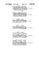
- FIGS. 1 through 8illustrate a preferred process of fabricating a field emitter array in accordance with the principles of the present invention.
- FIGS. 9 and 10illustrate additional processing steps employed in fabricating a field emission triode.
- FIGS. 1 and 2show side and top views, respectively, of a substrate 11 having field emitter elements 12 formed on a surface of the substrate.
- the substrate 11 and the field emitter elements 12may be of polysilicon, for example.
- the substrate 11is fabricated in a conventional manner to provide an array of emitter elements thereon, with FIG. 2 showing a typical field emitter array.
- the substrate 11 and the field emitter elements 12have a metal layer 20 disposed thereover.
- This metal layer 20may be of molybdenum, for example.
- the metal layer 20is typically deposited over elements 12 and substrate 11 to a thickness of from about 250 ⁇ to about 2000 ⁇ , for example. It should be understood, however, that the metal layer 20 may be eliminated in some applications.
- a layer of oxide 13is deposited over the surface of the substrate 11 and the field emitter elements 12 (or the metal layer 20 if it is employed).
- the oxide layer 13is typically formed using a chemical vapor deposition process.
- the oxide layer 13is deposited to a thickness of from about 5000 ⁇ to about 15000 ⁇ , for example.
- the chromium layermay have a thickness of from about 300 ⁇ to about 1000 ⁇ , while the gold layer may have a thickness of from about 2000 ⁇ to about 5000 ⁇ , for example.
- a layer of photoresist 15is then deposited over the gate metal layer 14.
- the layer of photoresist 15is typically deposited using a conventional spin-on procedure employing Hoechst AZ 1370 photoresist spun on at 4000 RPM for about 20 seconds, for example.
- FIG. 4The structure of FIG. 4 is then processed to cause portions of the layer of photoresist 15 above respective field emitter elements 12 to be removed, as shown in FIG. 5, and thereby expose respective portions of the gate metal layer 14 above respective tip regions of the field emitter elements 12.
- Thismay be accomplished by plasma etching the layer of photoresist 15 in an oxygen environment.
- the plasma etching operationmay be carried out in a plasma discharge stripping and etching system Model No. PDS/PDE-301 manufactured by LFE Corporation, Waltham, Mass., for example.
- the aforementioned plasma discharge systemmay be initially evacuated to a pressure of about 0.1 torr, after which a regulated flow of oxygen gas may be passed through the system at a flow rate of about 240 cc per minute and at a pressure of about 3 torr before commencement of the plasma discharge.
- a plasma dischargeis then established in the system for a predetermined time to achieve the desired photoresist removal.
- precisely-aligned openings 16are formed directly over respective field emitter elements 12 of the array.
- the size of the openings 16may be controlled by appropriately controlling process parameters, including time and power setting of the plasma discharge apparatus and/or the initial thickness of the layer of photoresist 15.
- the field emitter elements 12 that have been exposed via openings 16 in the preceding stepare then etched by means of a conventional etching procedure, for example, using the layer of photoresist 15 as a mask.
- a mixture of water and potassium iodidemay be employed for a time duration of from about 1 minute to about 5 minutes to etch the gold, for example, and potassium permanganate for about 7 seconds, and oxalic for about 7 seconds may be employed to etch the chromium, for example.
- the layer of photoresist 15is then removed, and the layer of oxide 13 is etched using a conventional etching procedure using buffered hydrogen fluoride, for example, to expose the field emitter elements 12. This results in a self-aligned cathode structure as shown in FIG. 8.
- FIGS. 9 and 10additional processing steps are illustrated that enable fabrication of a self-aligned anode structure above the field emission cathode structure fabricated pursuant to the process of FIGS. 1-8.
- a second layer of oxide 17is deposited on top of the gate metal layer 14, after which an additional layer of metal 18, which may serve as an anode metal layer in the resultant device, is deposited over the second layer of oxide 17.
- FIG. 9is processed in a manner described above with respect to FIGS. 4-8.
- a layer of photoresistis applied to the top surface of the anode metal layer 18 and is then plasma etched to remove portions of the layer of photoresist above the elements 12.
- the anode metal layer 18is then etched using the layer of photoresist as a mask.
- the layer of photoresistis then removed, and the first and second oxide layers 13,17 are etched to expose the field emitter elements 12, resulting in the structure shown in FIG. 10.
- the above-described embodimentsare merely illustrative of some of the many specific embodiments utilizing the principles of the present invention.
- numerous and other arrangementscan be readily devised by those skilled in the art without departing from the scope of the invention.
- metalmay be used instead of polysilicon to form the substrate and the emitter elements.
- dry etching of the oxide and metal layersmay be employed where anisotropic etching is critical.
- the gate metal layermay be comprised of metal alloys other than chromium and gold, such as by molybdenum, for example.
Landscapes
- Engineering & Computer Science (AREA)
- Manufacturing & Machinery (AREA)
- Cold Cathode And The Manufacture (AREA)
- Electrodes Of Semiconductors (AREA)
Abstract
Description
Claims (13)
Priority Applications (6)
| Application Number | Priority Date | Filing Date | Title |
|---|---|---|---|
| US07/393,199US4943343A (en) | 1989-08-14 | 1989-08-14 | Self-aligned gate process for fabricating field emitter arrays |
| CA002034481ACA2034481C (en) | 1989-08-14 | 1990-04-23 | Self-aligned gate process for fabricating field emitter arrays |
| DE69016397TDE69016397D1 (en) | 1989-08-14 | 1990-04-23 | METHOD FOR PRODUCING A FIELD EMITTER ARRANGEMENT WITH AUTOMATIC GATE ADJUSTMENT. |
| PCT/US1990/002184WO1991003066A1 (en) | 1989-08-14 | 1990-04-23 | Self-aligned gate process for fabricating field emitter arrays |
| EP90907546AEP0438544B1 (en) | 1989-08-14 | 1990-04-23 | Self-aligned gate process for fabricating field emitter arrays |
| IL94199AIL94199A0 (en) | 1989-08-14 | 1990-04-25 | Self-aligned gate process for fabricating field emitter arrays |
Applications Claiming Priority (1)
| Application Number | Priority Date | Filing Date | Title |
|---|---|---|---|
| US07/393,199US4943343A (en) | 1989-08-14 | 1989-08-14 | Self-aligned gate process for fabricating field emitter arrays |
Publications (1)
| Publication Number | Publication Date |
|---|---|
| US4943343Atrue US4943343A (en) | 1990-07-24 |
Family
ID=23553689
Family Applications (1)
| Application Number | Title | Priority Date | Filing Date |
|---|---|---|---|
| US07/393,199Expired - LifetimeUS4943343A (en) | 1989-08-14 | 1989-08-14 | Self-aligned gate process for fabricating field emitter arrays |
Country Status (6)
| Country | Link |
|---|---|
| US (1) | US4943343A (en) |
| EP (1) | EP0438544B1 (en) |
| CA (1) | CA2034481C (en) |
| DE (1) | DE69016397D1 (en) |
| IL (1) | IL94199A0 (en) |
| WO (1) | WO1991003066A1 (en) |
Cited By (53)
| Publication number | Priority date | Publication date | Assignee | Title |
|---|---|---|---|---|
| US5136205A (en)* | 1991-03-26 | 1992-08-04 | Hughes Aircraft Company | Microelectronic field emission device with air bridge anode |
| GB2254958A (en)* | 1991-01-25 | 1992-10-21 | Marconi Gec Ltd | Field emission devices. |
| US5181874A (en)* | 1991-03-26 | 1993-01-26 | Hughes Aircraft Company | Method of making microelectronic field emission device with air bridge anode |
| EP0525763A1 (en)* | 1991-08-01 | 1993-02-03 | Texas Instruments Incorporated | A method for building a vacuum microelectronics device |
| US5186670A (en)* | 1992-03-02 | 1993-02-16 | Micron Technology, Inc. | Method to form self-aligned gate structures and focus rings |
| US5199917A (en)* | 1991-12-09 | 1993-04-06 | Cornell Research Foundation, Inc. | Silicon tip field emission cathode arrays and fabrication thereof |
| US5199918A (en)* | 1991-11-07 | 1993-04-06 | Microelectronics And Computer Technology Corporation | Method of forming field emitter device with diamond emission tips |
| US5229331A (en)* | 1992-02-14 | 1993-07-20 | Micron Technology, Inc. | Method to form self-aligned gate structures around cold cathode emitter tips using chemical mechanical polishing technology |
| US5259799A (en)* | 1992-03-02 | 1993-11-09 | Micron Technology, Inc. | Method to form self-aligned gate structures and focus rings |
| US5266530A (en)* | 1991-11-08 | 1993-11-30 | Bell Communications Research, Inc. | Self-aligned gated electron field emitter |
| US5281891A (en)* | 1991-02-22 | 1994-01-25 | Matsushita Electric Industrial Co., Ltd. | Electron emission element |
| US5312514A (en)* | 1991-11-07 | 1994-05-17 | Microelectronics And Computer Technology Corporation | Method of making a field emitter device using randomly located nuclei as an etch mask |
| US5318918A (en)* | 1991-12-31 | 1994-06-07 | Texas Instruments Incorporated | Method of making an array of electron emitters |
| US5329207A (en)* | 1992-05-13 | 1994-07-12 | Micron Technology, Inc. | Field emission structures produced on macro-grain polysilicon substrates |
| US5382185A (en)* | 1993-03-31 | 1995-01-17 | The United States Of America As Represented By The Secretary Of The Navy | Thin-film edge field emitter device and method of manufacture therefor |
| US5399238A (en)* | 1991-11-07 | 1995-03-21 | Microelectronics And Computer Technology Corporation | Method of making field emission tips using physical vapor deposition of random nuclei as etch mask |
| US5445550A (en)* | 1993-12-22 | 1995-08-29 | Xie; Chenggang | Lateral field emitter device and method of manufacturing same |
| US5472916A (en)* | 1993-04-05 | 1995-12-05 | Siemens Aktiengesellschaft | Method for manufacturing tunnel-effect sensors |
| US5483741A (en)* | 1993-09-03 | 1996-01-16 | Micron Technology, Inc. | Method for fabricating a self limiting silicon based interconnect for testing bare semiconductor dice |
| US5494179A (en)* | 1993-01-22 | 1996-02-27 | Matsushita Electric Industrial Co., Ltd. | Field-emitter having a sharp apex and small-apertured gate and method for fabricating emitter |
| US5504385A (en)* | 1994-08-31 | 1996-04-02 | At&T Corp. | Spaced-gate emission device and method for making same |
| WO1996004674A3 (en)* | 1994-08-05 | 1996-05-02 | Central Research Lab Ltd | A self-aligned gate field emitter device and methods for producing the same |
| US5536193A (en)* | 1991-11-07 | 1996-07-16 | Microelectronics And Computer Technology Corporation | Method of making wide band gap field emitter |
| US5584740A (en)* | 1993-03-31 | 1996-12-17 | The United States Of America As Represented By The Secretary Of The Navy | Thin-film edge field emitter device and method of manufacture therefor |
| US5592736A (en)* | 1993-09-03 | 1997-01-14 | Micron Technology, Inc. | Fabricating an interconnect for testing unpackaged semiconductor dice having raised bond pads |
| US5600200A (en)* | 1992-03-16 | 1997-02-04 | Microelectronics And Computer Technology Corporation | Wire-mesh cathode |
| US5601966A (en)* | 1993-11-04 | 1997-02-11 | Microelectronics And Computer Technology Corporation | Methods for fabricating flat panel display systems and components |
| US5612712A (en)* | 1992-03-16 | 1997-03-18 | Microelectronics And Computer Technology Corporation | Diode structure flat panel display |
| US5627427A (en)* | 1991-12-09 | 1997-05-06 | Cornell Research Foundation, Inc. | Silicon tip field emission cathodes |
| US5635081A (en) | 1994-07-12 | 1997-06-03 | Nec Corporation | Fabrication method of field-emission cold cathode |
| US5653619A (en)* | 1992-03-02 | 1997-08-05 | Micron Technology, Inc. | Method to form self-aligned gate structures and focus rings |
| US5669801A (en)* | 1995-09-28 | 1997-09-23 | Texas Instruments Incorporated | Field emission device cathode and method of fabrication |
| US5675216A (en)* | 1992-03-16 | 1997-10-07 | Microelectronics And Computer Technololgy Corp. | Amorphic diamond film flat field emission cathode |
| US5683282A (en)* | 1995-12-04 | 1997-11-04 | Industrial Technology Research Institute | Method for manufacturing flat cold cathode arrays |
| US5696028A (en)* | 1992-02-14 | 1997-12-09 | Micron Technology, Inc. | Method to form an insulative barrier useful in field emission displays for reducing surface leakage |
| US5727976A (en)* | 1994-03-15 | 1998-03-17 | Kabushiki Kaisha Toshiba | Method of producing micro vacuum tube having cold emitter |
| US5775968A (en)* | 1993-06-14 | 1998-07-07 | Fujitsu Limited | Cathode device having smaller opening |
| US5844251A (en)* | 1994-01-05 | 1998-12-01 | Cornell Research Foundation, Inc. | High aspect ratio probes with self-aligned control electrodes |
| US5857884A (en)* | 1996-02-07 | 1999-01-12 | Micron Display Technology, Inc. | Photolithographic technique of emitter tip exposure in FEDS |
| US6022256A (en)* | 1996-11-06 | 2000-02-08 | Micron Display Technology, Inc. | Field emission display and method of making same |
| US6049089A (en)* | 1993-07-07 | 2000-04-11 | Micron Technology, Inc. | Electron emitters and method for forming them |
| US6127773A (en)* | 1992-03-16 | 2000-10-03 | Si Diamond Technology, Inc. | Amorphic diamond film flat field emission cathode |
| US6197607B1 (en)* | 1999-03-01 | 2001-03-06 | Micron Technology, Inc. | Method of fabricating field emission arrays to optimize the size of grid openings and to minimize the occurrence of electrical shorts |
| EP1115134A1 (en)* | 2000-01-05 | 2001-07-11 | Samsung SDI Co. Ltd. | Field emission device and method for fabricating the same |
| US6281621B1 (en)* | 1992-07-14 | 2001-08-28 | Kabushiki Kaisha Toshiba | Field emission cathode structure, method for production thereof, and flat panel display device using same |
| US6376833B2 (en)* | 1997-08-26 | 2002-04-23 | Canon Kabushiki Kaisha | Projection having a micro-aperture, probe or multi-probe having such a projection and surface scanner, aligner or information processor comprising such a probe |
| US6394871B2 (en)* | 1998-09-02 | 2002-05-28 | Micron Technology, Inc. | Method for reducing emitter tip to gate spacing in field emission devices |
| US6414506B2 (en) | 1993-09-03 | 2002-07-02 | Micron Technology, Inc. | Interconnect for testing semiconductor dice having raised bond pads |
| US20030049899A1 (en)* | 2001-09-13 | 2003-03-13 | Microsaic Systems Limited | Electrode structures |
| US6555402B2 (en) | 1999-04-29 | 2003-04-29 | Micron Technology, Inc. | Self-aligned field extraction grid and method of forming |
| US6629869B1 (en) | 1992-03-16 | 2003-10-07 | Si Diamond Technology, Inc. | Method of making flat panel displays having diamond thin film cathode |
| CN102130122B (en)* | 2010-01-20 | 2012-08-01 | 上海华虹Nec电子有限公司 | Domain structure of silicon germanium heterojunction triode |
| CN110104609A (en)* | 2019-05-10 | 2019-08-09 | 中国科学院微电子研究所 | A kind of microelectrode and forming method thereof |
Families Citing this family (2)
| Publication number | Priority date | Publication date | Assignee | Title |
|---|---|---|---|---|
| US5270574A (en)* | 1991-08-01 | 1993-12-14 | Texas Instruments Incorporated | Vacuum micro-chamber for encapsulating a microelectronics device |
| DE69205753T2 (en)* | 1991-08-01 | 1996-05-30 | Texas Instruments Inc | Process for forming vacuum microchambers for embedding microelectronic devices. |
Citations (8)
| Publication number | Priority date | Publication date | Assignee | Title |
|---|---|---|---|---|
| US3453478A (en)* | 1966-05-31 | 1969-07-01 | Stanford Research Inst | Needle-type electron source |
| US3665241A (en)* | 1970-07-13 | 1972-05-23 | Stanford Research Inst | Field ionizer and field emission cathode structures and methods of production |
| US3755704A (en)* | 1970-02-06 | 1973-08-28 | Stanford Research Inst | Field emission cathode structures and devices utilizing such structures |
| US3921022A (en)* | 1974-09-03 | 1975-11-18 | Rca Corp | Field emitting device and method of making same |
| US3998678A (en)* | 1973-03-22 | 1976-12-21 | Hitachi, Ltd. | Method of manufacturing thin-film field-emission electron source |
| US4008412A (en)* | 1974-08-16 | 1977-02-15 | Hitachi, Ltd. | Thin-film field-emission electron source and a method for manufacturing the same |
| US4307507A (en)* | 1980-09-10 | 1981-12-29 | The United States Of America As Represented By The Secretary Of The Navy | Method of manufacturing a field-emission cathode structure |
| US4513308A (en)* | 1982-09-23 | 1985-04-23 | The United States Of America As Represented By The Secretary Of The Navy | p-n Junction controlled field emitter array cathode |
Family Cites Families (1)
| Publication number | Priority date | Publication date | Assignee | Title |
|---|---|---|---|---|
| GB8720792D0 (en)* | 1987-09-04 | 1987-10-14 | Gen Electric Co Plc | Vacuum devices |
- 1989
- 1989-08-14USUS07/393,199patent/US4943343A/ennot_activeExpired - Lifetime
- 1990
- 1990-04-23EPEP90907546Apatent/EP0438544B1/ennot_activeExpired - Lifetime
- 1990-04-23DEDE69016397Tpatent/DE69016397D1/ennot_activeExpired - Lifetime
- 1990-04-23WOPCT/US1990/002184patent/WO1991003066A1/enactiveIP Right Grant
- 1990-04-23CACA002034481Apatent/CA2034481C/ennot_activeExpired - Fee Related
- 1990-04-25ILIL94199Apatent/IL94199A0/ennot_activeIP Right Cessation
Patent Citations (8)
| Publication number | Priority date | Publication date | Assignee | Title |
|---|---|---|---|---|
| US3453478A (en)* | 1966-05-31 | 1969-07-01 | Stanford Research Inst | Needle-type electron source |
| US3755704A (en)* | 1970-02-06 | 1973-08-28 | Stanford Research Inst | Field emission cathode structures and devices utilizing such structures |
| US3665241A (en)* | 1970-07-13 | 1972-05-23 | Stanford Research Inst | Field ionizer and field emission cathode structures and methods of production |
| US3998678A (en)* | 1973-03-22 | 1976-12-21 | Hitachi, Ltd. | Method of manufacturing thin-film field-emission electron source |
| US4008412A (en)* | 1974-08-16 | 1977-02-15 | Hitachi, Ltd. | Thin-film field-emission electron source and a method for manufacturing the same |
| US3921022A (en)* | 1974-09-03 | 1975-11-18 | Rca Corp | Field emitting device and method of making same |
| US4307507A (en)* | 1980-09-10 | 1981-12-29 | The United States Of America As Represented By The Secretary Of The Navy | Method of manufacturing a field-emission cathode structure |
| US4513308A (en)* | 1982-09-23 | 1985-04-23 | The United States Of America As Represented By The Secretary Of The Navy | p-n Junction controlled field emitter array cathode |
Non-Patent Citations (8)
| Title |
|---|
| C. A. Spindt et al., "Physical Properties of Thin-Film Field Emission Cathodes with Molybdenum Cones", Journal of Applied Physics, vol. 47, No. 12, Dec. 1976, pp. 5248-5263. |
| C. A. Spindt et al., "Recent Progress in Low-Voltage Field-Emission Cathode Development", Journal de Physique, vol. 45, No. C-9, Dec. 1984, pp. 269-278. |
| C. A. Spindt et al., Physical Properties of Thin Film Field Emission Cathodes with Molybdenum Cones , Journal of Applied Physics, vol. 47, No. 12, Dec. 1976, pp. 5248 5263.* |
| C. A. Spindt et al., Recent Progress in Low Voltage Field Emission Cathode Development , Journal de Physique, vol. 45, No. C 9, Dec. 1984, pp. 269 278.* |
| C. A. Spindt, "A Thin-Film Field-Emission Cathode", Journal of Applied Physics, vol. 39, No. 7, Jun. 1986, pp. 3504-3505. |
| C. A. Spindt, A Thin Film Field Emission Cathode , Journal of Applied Physics, vol. 39, No. 7, Jun. 1986, pp. 3504 3505.* |
| Gray et al., "A Vacuum Field Effect Transistor Using Silicon Field Emitter Arrays", IEDM, 1986, pp. 776-779. |
| Gray et al., A Vacuum Field Effect Transistor Using Silicon Field Emitter Arrays , IEDM, 1986, pp. 776 779.* |
Cited By (98)
| Publication number | Priority date | Publication date | Assignee | Title |
|---|---|---|---|---|
| GB2254958B (en)* | 1991-01-25 | 1994-12-14 | Marconi Gec Ltd | Field emission devices |
| GB2254958A (en)* | 1991-01-25 | 1992-10-21 | Marconi Gec Ltd | Field emission devices. |
| US5228877A (en)* | 1991-01-25 | 1993-07-20 | Gec-Marconi Limited | Field emission devices |
| US5281891A (en)* | 1991-02-22 | 1994-01-25 | Matsushita Electric Industrial Co., Ltd. | Electron emission element |
| US5181874A (en)* | 1991-03-26 | 1993-01-26 | Hughes Aircraft Company | Method of making microelectronic field emission device with air bridge anode |
| US5136205A (en)* | 1991-03-26 | 1992-08-04 | Hughes Aircraft Company | Microelectronic field emission device with air bridge anode |
| EP0525763A1 (en)* | 1991-08-01 | 1993-02-03 | Texas Instruments Incorporated | A method for building a vacuum microelectronics device |
| US5411426A (en)* | 1991-08-01 | 1995-05-02 | Texas Instruments Incorporated | Vacuum microelectronics device and method for building the same |
| US5349217A (en)* | 1991-08-01 | 1994-09-20 | Texas Instruments Incorporated | Vacuum microelectronics device |
| US5199918A (en)* | 1991-11-07 | 1993-04-06 | Microelectronics And Computer Technology Corporation | Method of forming field emitter device with diamond emission tips |
| US5861707A (en)* | 1991-11-07 | 1999-01-19 | Si Diamond Technology, Inc. | Field emitter with wide band gap emission areas and method of using |
| US5536193A (en)* | 1991-11-07 | 1996-07-16 | Microelectronics And Computer Technology Corporation | Method of making wide band gap field emitter |
| US5399238A (en)* | 1991-11-07 | 1995-03-21 | Microelectronics And Computer Technology Corporation | Method of making field emission tips using physical vapor deposition of random nuclei as etch mask |
| US5341063A (en)* | 1991-11-07 | 1994-08-23 | Microelectronics And Computer Technology Corporation | Field emitter with diamond emission tips |
| US5312514A (en)* | 1991-11-07 | 1994-05-17 | Microelectronics And Computer Technology Corporation | Method of making a field emitter device using randomly located nuclei as an etch mask |
| US5266530A (en)* | 1991-11-08 | 1993-11-30 | Bell Communications Research, Inc. | Self-aligned gated electron field emitter |
| US5199917A (en)* | 1991-12-09 | 1993-04-06 | Cornell Research Foundation, Inc. | Silicon tip field emission cathode arrays and fabrication thereof |
| US5627427A (en)* | 1991-12-09 | 1997-05-06 | Cornell Research Foundation, Inc. | Silicon tip field emission cathodes |
| US5455196A (en)* | 1991-12-31 | 1995-10-03 | Texas Instruments Incorporated | Method of forming an array of electron emitters |
| US5318918A (en)* | 1991-12-31 | 1994-06-07 | Texas Instruments Incorporated | Method of making an array of electron emitters |
| DE4304103A1 (en)* | 1992-02-14 | 1993-08-19 | Micron Technology Inc | |
| US5229331A (en)* | 1992-02-14 | 1993-07-20 | Micron Technology, Inc. | Method to form self-aligned gate structures around cold cathode emitter tips using chemical mechanical polishing technology |
| US5372973A (en)* | 1992-02-14 | 1994-12-13 | Micron Technology, Inc. | Method to form self-aligned gate structures around cold cathode emitter tips using chemical mechanical polishing technology |
| DE4304103C2 (en)* | 1992-02-14 | 2002-02-14 | Micron Technology Inc | Process for forming self-aligned gate structures |
| US5696028A (en)* | 1992-02-14 | 1997-12-09 | Micron Technology, Inc. | Method to form an insulative barrier useful in field emission displays for reducing surface leakage |
| US5831378A (en)* | 1992-02-14 | 1998-11-03 | Micron Technology, Inc. | Insulative barrier useful in field emission displays for reducing surface leakage |
| US6066507A (en)* | 1992-02-14 | 2000-05-23 | Micron Technology, Inc. | Method to form an insulative barrier useful in field emission displays for reducing surface leakage |
| EP0559156A1 (en)* | 1992-03-02 | 1993-09-08 | Micron Technology, Inc. | Method to form self-aligned gate structures and focus rings |
| US5259799A (en)* | 1992-03-02 | 1993-11-09 | Micron Technology, Inc. | Method to form self-aligned gate structures and focus rings |
| US5653619A (en)* | 1992-03-02 | 1997-08-05 | Micron Technology, Inc. | Method to form self-aligned gate structures and focus rings |
| US5186670A (en)* | 1992-03-02 | 1993-02-16 | Micron Technology, Inc. | Method to form self-aligned gate structures and focus rings |
| US5612712A (en)* | 1992-03-16 | 1997-03-18 | Microelectronics And Computer Technology Corporation | Diode structure flat panel display |
| US6127773A (en)* | 1992-03-16 | 2000-10-03 | Si Diamond Technology, Inc. | Amorphic diamond film flat field emission cathode |
| US5703435A (en)* | 1992-03-16 | 1997-12-30 | Microelectronics & Computer Technology Corp. | Diamond film flat field emission cathode |
| US5686791A (en)* | 1992-03-16 | 1997-11-11 | Microelectronics And Computer Technology Corp. | Amorphic diamond film flat field emission cathode |
| US6629869B1 (en) | 1992-03-16 | 2003-10-07 | Si Diamond Technology, Inc. | Method of making flat panel displays having diamond thin film cathode |
| US5675216A (en)* | 1992-03-16 | 1997-10-07 | Microelectronics And Computer Technololgy Corp. | Amorphic diamond film flat field emission cathode |
| US5600200A (en)* | 1992-03-16 | 1997-02-04 | Microelectronics And Computer Technology Corporation | Wire-mesh cathode |
| US5438240A (en)* | 1992-05-13 | 1995-08-01 | Micron Technology, Inc. | Field emission structures produced on macro-grain polysilicon substrates |
| US5329207A (en)* | 1992-05-13 | 1994-07-12 | Micron Technology, Inc. | Field emission structures produced on macro-grain polysilicon substrates |
| US6281621B1 (en)* | 1992-07-14 | 2001-08-28 | Kabushiki Kaisha Toshiba | Field emission cathode structure, method for production thereof, and flat panel display device using same |
| US5494179A (en)* | 1993-01-22 | 1996-02-27 | Matsushita Electric Industrial Co., Ltd. | Field-emitter having a sharp apex and small-apertured gate and method for fabricating emitter |
| US5584740A (en)* | 1993-03-31 | 1996-12-17 | The United States Of America As Represented By The Secretary Of The Navy | Thin-film edge field emitter device and method of manufacture therefor |
| US5382185A (en)* | 1993-03-31 | 1995-01-17 | The United States Of America As Represented By The Secretary Of The Navy | Thin-film edge field emitter device and method of manufacture therefor |
| US5472916A (en)* | 1993-04-05 | 1995-12-05 | Siemens Aktiengesellschaft | Method for manufacturing tunnel-effect sensors |
| US5775968A (en)* | 1993-06-14 | 1998-07-07 | Fujitsu Limited | Cathode device having smaller opening |
| US6140760A (en)* | 1993-06-14 | 2000-10-31 | Fujitsu Limited | Cathode device having smaller opening |
| US7064476B2 (en) | 1993-07-07 | 2006-06-20 | Micron Technology, Inc. | Emitter |
| US20070052339A1 (en)* | 1993-07-07 | 2007-03-08 | Cathey David A | Electron emitters with dopant gradient |
| US20060237812A1 (en)* | 1993-07-07 | 2006-10-26 | Cathey David A | Electronic emitters with dopant gradient |
| US20060226765A1 (en)* | 1993-07-07 | 2006-10-12 | Cathey David A | Electronic emitters with dopant gradient |
| US6049089A (en)* | 1993-07-07 | 2000-04-11 | Micron Technology, Inc. | Electron emitters and method for forming them |
| US20050023951A1 (en)* | 1993-07-07 | 2005-02-03 | Cathey David A. | Electron emitters with dopant gradient |
| US6825596B1 (en) | 1993-07-07 | 2004-11-30 | Micron Technology, Inc. | Electron emitters with dopant gradient |
| US5483741A (en)* | 1993-09-03 | 1996-01-16 | Micron Technology, Inc. | Method for fabricating a self limiting silicon based interconnect for testing bare semiconductor dice |
| US5592736A (en)* | 1993-09-03 | 1997-01-14 | Micron Technology, Inc. | Fabricating an interconnect for testing unpackaged semiconductor dice having raised bond pads |
| US6414506B2 (en) | 1993-09-03 | 2002-07-02 | Micron Technology, Inc. | Interconnect for testing semiconductor dice having raised bond pads |
| US5601966A (en)* | 1993-11-04 | 1997-02-11 | Microelectronics And Computer Technology Corporation | Methods for fabricating flat panel display systems and components |
| US5652083A (en)* | 1993-11-04 | 1997-07-29 | Microelectronics And Computer Technology Corporation | Methods for fabricating flat panel display systems and components |
| US5614353A (en)* | 1993-11-04 | 1997-03-25 | Si Diamond Technology, Inc. | Methods for fabricating flat panel display systems and components |
| US5445550A (en)* | 1993-12-22 | 1995-08-29 | Xie; Chenggang | Lateral field emitter device and method of manufacturing same |
| US5528099A (en)* | 1993-12-22 | 1996-06-18 | Microelectronics And Computer Technology Corporation | Lateral field emitter device |
| US6027951A (en)* | 1994-01-05 | 2000-02-22 | Macdonald; Noel C. | Method of making high aspect ratio probes with self-aligned control electrodes |
| US5844251A (en)* | 1994-01-05 | 1998-12-01 | Cornell Research Foundation, Inc. | High aspect ratio probes with self-aligned control electrodes |
| US5727976A (en)* | 1994-03-15 | 1998-03-17 | Kabushiki Kaisha Toshiba | Method of producing micro vacuum tube having cold emitter |
| US5635081A (en) | 1994-07-12 | 1997-06-03 | Nec Corporation | Fabrication method of field-emission cold cathode |
| WO1996004674A3 (en)* | 1994-08-05 | 1996-05-02 | Central Research Lab Ltd | A self-aligned gate field emitter device and methods for producing the same |
| US5818153A (en)* | 1994-08-05 | 1998-10-06 | Central Research Laboratories Limited | Self-aligned gate field emitter device and methods for producing the same |
| US5681196A (en)* | 1994-08-31 | 1997-10-28 | Lucent Technologies Inc. | Spaced-gate emission device and method for making same |
| US5504385A (en)* | 1994-08-31 | 1996-04-02 | At&T Corp. | Spaced-gate emission device and method for making same |
| US5669801A (en)* | 1995-09-28 | 1997-09-23 | Texas Instruments Incorporated | Field emission device cathode and method of fabrication |
| US5791962A (en)* | 1995-12-04 | 1998-08-11 | Industrial Technology Research Institute | Methods for manufacturing flat cold cathode arrays |
| US5820433A (en)* | 1995-12-04 | 1998-10-13 | Industrial Technology Research Institute | Methods for manufacturing flat cold cathode arrays |
| US5683282A (en)* | 1995-12-04 | 1997-11-04 | Industrial Technology Research Institute | Method for manufacturing flat cold cathode arrays |
| US5857884A (en)* | 1996-02-07 | 1999-01-12 | Micron Display Technology, Inc. | Photolithographic technique of emitter tip exposure in FEDS |
| US6022256A (en)* | 1996-11-06 | 2000-02-08 | Micron Display Technology, Inc. | Field emission display and method of making same |
| US6181060B1 (en) | 1996-11-06 | 2001-01-30 | Micron Technology, Inc. | Field emission display with plural dielectric layers |
| US6376833B2 (en)* | 1997-08-26 | 2002-04-23 | Canon Kabushiki Kaisha | Projection having a micro-aperture, probe or multi-probe having such a projection and surface scanner, aligner or information processor comprising such a probe |
| US6394871B2 (en)* | 1998-09-02 | 2002-05-28 | Micron Technology, Inc. | Method for reducing emitter tip to gate spacing in field emission devices |
| US6710539B2 (en) | 1998-09-02 | 2004-03-23 | Micron Technology, Inc. | Field emission devices having structure for reduced emitter tip to gate spacing |
| US6197607B1 (en)* | 1999-03-01 | 2001-03-06 | Micron Technology, Inc. | Method of fabricating field emission arrays to optimize the size of grid openings and to minimize the occurrence of electrical shorts |
| US6498425B1 (en) | 1999-03-01 | 2002-12-24 | Micron Technology, Inc. | Field emission array with planarized lower dielectric layer |
| US20040023592A1 (en)* | 1999-03-01 | 2004-02-05 | Ammar Derraa | Field emission arrays and method of fabricating same to optimize the size of grid openings and to minimize the occurrence of electrical shorts |
| US6403390B2 (en) | 1999-03-01 | 2002-06-11 | Micron Technology, Inc. | Method of fabricating field emission arrays to optimize the size of grid openings and to minimize the occurrence of electrical shorts |
| US6589803B2 (en) | 1999-03-01 | 2003-07-08 | Micron Technology, Inc. | Field emission arrays and method of fabricating same to optimize the size of grid openings and to minimize the occurrence of electrical shorts |
| US6731063B2 (en) | 1999-03-01 | 2004-05-04 | Micron Technology, Inc. | Field emission arrays to optimize the size of grid openings and to minimize the occurrence of electrical shorts |
| US6875626B2 (en) | 1999-03-01 | 2005-04-05 | Micron Technology, Inc. | Field emission arrays and method of fabricating same to optimize the size of grid openings and to minimize the occurrence of electrical shorts |
| US6555402B2 (en) | 1999-04-29 | 2003-04-29 | Micron Technology, Inc. | Self-aligned field extraction grid and method of forming |
| US6927534B2 (en) | 2000-01-05 | 2005-08-09 | Samsung Sdi Co., Ltd. | Field emission device |
| US6632114B2 (en) | 2000-01-05 | 2003-10-14 | Samsung Sdi Co., Ltd. | Method for manufacturing field emission device |
| US20040027052A1 (en)* | 2000-01-05 | 2004-02-12 | Samsung Sdi Co., Ltd. | Field emission device |
| EP1115134A1 (en)* | 2000-01-05 | 2001-07-11 | Samsung SDI Co. Ltd. | Field emission device and method for fabricating the same |
| GB2383187A (en)* | 2001-09-13 | 2003-06-18 | Microsaic Systems Ltd | Knife-edge cold cathode field emitter |
| GB2383187B (en)* | 2001-09-13 | 2005-06-22 | Microsaic Systems Ltd | Electrode structures |
| US6924158B2 (en) | 2001-09-13 | 2005-08-02 | Microsaic Systems Limited | Electrode structures |
| US20030049899A1 (en)* | 2001-09-13 | 2003-03-13 | Microsaic Systems Limited | Electrode structures |
| CN102130122B (en)* | 2010-01-20 | 2012-08-01 | 上海华虹Nec电子有限公司 | Domain structure of silicon germanium heterojunction triode |
| CN110104609A (en)* | 2019-05-10 | 2019-08-09 | 中国科学院微电子研究所 | A kind of microelectrode and forming method thereof |
Also Published As
| Publication number | Publication date |
|---|---|
| CA2034481C (en) | 1993-10-05 |
| EP0438544B1 (en) | 1995-01-25 |
| IL94199A0 (en) | 1991-01-31 |
| WO1991003066A1 (en) | 1991-03-07 |
| CA2034481A1 (en) | 1991-02-15 |
| EP0438544A1 (en) | 1991-07-31 |
| DE69016397D1 (en) | 1995-03-09 |
Similar Documents
| Publication | Publication Date | Title |
|---|---|---|
| US4943343A (en) | Self-aligned gate process for fabricating field emitter arrays | |
| US5151061A (en) | Method to form self-aligned tips for flat panel displays | |
| US4307507A (en) | Method of manufacturing a field-emission cathode structure | |
| US5865657A (en) | Fabrication of gated electron-emitting device utilizing distributed particles to form gate openings typically beveled and/or combined with lift-off or electrochemical removal of excess emitter material | |
| US5057047A (en) | Low capacitance field emitter array and method of manufacture therefor | |
| US5150192A (en) | Field emitter array | |
| US5696385A (en) | Field emission device having reduced row-to-column leakage | |
| EP0468036A1 (en) | ENCLOSED FIELD EMISSION DEVICE IN ESSENTIAL ORTHOGONAL VAPOR DEPOSITION. | |
| US5409568A (en) | Method of fabricating a microelectronic vacuum triode structure | |
| US6495955B1 (en) | Structure and method for improved field emitter arrays | |
| US6737793B2 (en) | Apparatus for emitting electrons comprising a subsurface emitter structure | |
| US5607335A (en) | Fabrication of electron-emitting structures using charged-particle tracks and removal of emitter material | |
| US6045678A (en) | Formation of nanofilament field emission devices | |
| JPH0831308A (en) | Manufacture of electric field emission cold cathode | |
| JP3086445B2 (en) | Method of forming field emission device | |
| JP2000173444A (en) | Electric field emitting type cold negative electrode, and its manufacture | |
| KR100186253B1 (en) | Method of manufacturing silicon fea by locos | |
| KR100290136B1 (en) | Field emission device manufacturing method | |
| JPH04505073A (en) | Self-aligned gate method for manufacturing field emitter arrays | |
| KR100236658B1 (en) | How to make a triode volcanic emitter | |
| JP3457054B2 (en) | Method of manufacturing rod-shaped silicon structure | |
| JP2737675B2 (en) | Manufacturing method of vertical micro cold cathode | |
| JPH04262337A (en) | Manufacture of electric field emitting cathode | |
| JPH06325691A (en) | Manufacture of fine vacuum element | |
| JPH08328236A (en) | Production of transfer mask |
Legal Events
| Date | Code | Title | Description |
|---|---|---|---|
| AS | Assignment | Owner name:HUGHES AIRCRAFT COMPANY, CALIFORNIA Free format text:ASSIGNMENT OF ASSIGNORS INTEREST.;ASSIGNORS:BARDAI, ZAHER;ROLPH, RANDY K.;LAMB, ARLENE E.;AND OTHERS;REEL/FRAME:005117/0201 Effective date:19890801 | |
| FPAY | Fee payment | Year of fee payment:4 | |
| REMI | Maintenance fee reminder mailed | ||
| AS | Assignment | Owner name:HUGHES ELECTRONICS CORPORATION, CALIFORNIA Free format text:ASSIGNMENT OF ASSIGNORS INTEREST;ASSIGNOR:HE HOLDINGS INC., HUGHES ELECTRONICS, FORMERLY KNOWN AS HUGHES AIRCRAFT COMPANY;REEL/FRAME:009123/0473 Effective date:19971216 | |
| FP | Lapsed due to failure to pay maintenance fee | Effective date:19980729 | |
| FEPP | Fee payment procedure | Free format text:PETITION RELATED TO MAINTENANCE FEES FILED (ORIGINAL EVENT CODE: PMFP); ENTITY STATUS OF PATENT OWNER: LARGE ENTITY | |
| FEPP | Fee payment procedure | Free format text:PETITION RELATED TO MAINTENANCE FEES GRANTED (ORIGINAL EVENT CODE: PMFG); ENTITY STATUS OF PATENT OWNER: LARGE ENTITY | |
| FPAY | Fee payment | Year of fee payment:8 | |
| SULP | Surcharge for late payment | ||
| STCF | Information on status: patent grant | Free format text:PATENTED CASE | |
| PRDP | Patent reinstated due to the acceptance of a late maintenance fee | Effective date:20000512 | |
| FEPP | Fee payment procedure | Free format text:PAYER NUMBER DE-ASSIGNED (ORIGINAL EVENT CODE: RMPN); ENTITY STATUS OF PATENT OWNER: LARGE ENTITY Free format text:PAYOR NUMBER ASSIGNED (ORIGINAL EVENT CODE: ASPN); ENTITY STATUS OF PATENT OWNER: LARGE ENTITY | |
| FPAY | Fee payment | Year of fee payment:12 | |
| AS | Assignment | Owner name:BOEING COMPANY, THE, ILLINOIS Free format text:ASSIGNMENT OF ASSIGNORS INTEREST;ASSIGNOR:HUGHES ELECTRONICS CORPORATION;REEL/FRAME:015428/0184 Effective date:20000905 | |
| AS | Assignment | Owner name:BOEING ELECTRON DYNAMIC DEVICES, INC., CALIFORNIA Free format text:ASSIGNMENT OF ASSIGNORS INTEREST;ASSIGNOR:THE BOEING COMPANY;REEL/FRAME:017649/0130 Effective date:20050228 | |
| AS | Assignment | Owner name:L-3 COMMUNICATIONS ELECTRON TECHNOLOGIES, INC., CA Free format text:CHANGE OF NAME;ASSIGNOR:BOEING ELECTRON DYNAMIC DEVICES, INC.;REEL/FRAME:017706/0155 Effective date:20050228 |