US4942076A - Ceramic substrate with metal filled via holes for hybrid microcircuits and method of making the same - Google Patents
Ceramic substrate with metal filled via holes for hybrid microcircuits and method of making the sameDownload PDFInfo
- Publication number
- US4942076A US4942076AUS07/266,669US26666988AUS4942076AUS 4942076 AUS4942076 AUS 4942076AUS 26666988 AUS26666988 AUS 26666988AUS 4942076 AUS4942076 AUS 4942076A
- Authority
- US
- United States
- Prior art keywords
- via holes
- metal
- paste
- substrate
- sheet
- Prior art date
- Legal status (The legal status is an assumption and is not a legal conclusion. Google has not performed a legal analysis and makes no representation as to the accuracy of the status listed.)
- Expired - Lifetime
Links
- 239000000758substrateSubstances0.000titleclaimsabstractdescription145
- 229910052751metalInorganic materials0.000titleclaimsabstractdescription133
- 239000002184metalSubstances0.000titleclaimsabstractdescription133
- 239000000919ceramicSubstances0.000titleclaimsdescription34
- 238000004519manufacturing processMethods0.000titleclaims6
- PNEYBMLMFCGWSK-UHFFFAOYSA-Naluminium oxideInorganic materials[O-2].[O-2].[O-2].[Al+3].[Al+3]PNEYBMLMFCGWSK-UHFFFAOYSA-N0.000claimsabstractdescription89
- 229910001218Gallium arsenideInorganic materials0.000claimsabstractdescription60
- 229910052721tungstenInorganic materials0.000claimsabstractdescription43
- WFKWXMTUELFFGS-UHFFFAOYSA-NtungstenChemical compound[W]WFKWXMTUELFFGS-UHFFFAOYSA-N0.000claimsabstractdescription40
- 239000010937tungstenSubstances0.000claimsabstractdescription40
- 239000010949copperSubstances0.000claimsabstractdescription35
- 239000011230binding agentSubstances0.000claimsabstractdescription25
- 229910052802copperInorganic materials0.000claimsabstractdescription23
- RYGMFSIKBFXOCR-UHFFFAOYSA-NCopperChemical compound[Cu]RYGMFSIKBFXOCR-UHFFFAOYSA-N0.000claimsabstractdescription22
- 239000000203mixtureSubstances0.000claimsabstractdescription19
- 238000000034methodMethods0.000claimsabstractdescription17
- 239000011148porous materialSubstances0.000claimsabstractdescription10
- 238000007789sealingMethods0.000claimsabstractdescription3
- 239000002131composite materialSubstances0.000claimsdescription29
- 239000003870refractory metalSubstances0.000claimsdescription26
- 239000002245particleSubstances0.000claimsdescription22
- 239000000463materialSubstances0.000claimsdescription21
- 230000008018meltingEffects0.000claimsdescription14
- 238000002844meltingMethods0.000claimsdescription14
- 239000004065semiconductorSubstances0.000claimsdescription13
- 239000007787solidSubstances0.000claimsdescription11
- 238000000151depositionMethods0.000claimsdescription7
- 238000010438heat treatmentMethods0.000claimsdescription7
- 238000005245sinteringMethods0.000claimsdescription5
- 229910052737goldInorganic materials0.000claimsdescription4
- 239000010931goldSubstances0.000claimsdescription4
- 229910052709silverInorganic materials0.000claimsdescription4
- 229910052750molybdenumInorganic materials0.000claimsdescription3
- 238000005498polishingMethods0.000claimsdescription3
- ZOKXTWBITQBERF-UHFFFAOYSA-NMolybdenumChemical compound[Mo]ZOKXTWBITQBERF-UHFFFAOYSA-N0.000claimsdescription2
- PCHJSUWPFVWCPO-UHFFFAOYSA-NgoldChemical compound[Au]PCHJSUWPFVWCPO-UHFFFAOYSA-N0.000claimsdescription2
- 239000011733molybdenumSubstances0.000claimsdescription2
- 239000012777electrically insulating materialSubstances0.000claims17
- 239000012255powdered metalSubstances0.000claims4
- 238000005553drillingMethods0.000claims2
- 239000004332silverSubstances0.000claims2
- 229910001316Ag alloyInorganic materials0.000claims1
- 229910001020Au alloyInorganic materials0.000claims1
- BQCADISMDOOEFD-UHFFFAOYSA-NSilverChemical compound[Ag]BQCADISMDOOEFD-UHFFFAOYSA-N0.000claims1
- 239000004020conductorSubstances0.000claims1
- 239000002923metal particleSubstances0.000claims1
- JBRZTFJDHDCESZ-UHFFFAOYSA-NAsGaChemical compound[As]#[Ga]JBRZTFJDHDCESZ-UHFFFAOYSA-N0.000description55
- 239000010409thin filmSubstances0.000description21
- 150000002739metalsChemical class0.000description5
- IJGRMHOSHXDMSA-UHFFFAOYSA-NAtomic nitrogenChemical compoundN#NIJGRMHOSHXDMSA-UHFFFAOYSA-N0.000description4
- 239000002904solventSubstances0.000description3
- UFHFLCQGNIYNRP-UHFFFAOYSA-NHydrogenChemical compound[H][H]UFHFLCQGNIYNRP-UHFFFAOYSA-N0.000description2
- 238000005219brazingMethods0.000description2
- 238000010276constructionMethods0.000description2
- 230000001419dependent effectEffects0.000description2
- 239000010408filmSubstances0.000description2
- 239000001257hydrogenSubstances0.000description2
- 229910052739hydrogenInorganic materials0.000description2
- 229910052757nitrogenInorganic materials0.000description2
- 239000007858starting materialSubstances0.000description2
- -1Ag and AuChemical class0.000description1
- 229910002696Ag-AuInorganic materials0.000description1
- RTAQQCXQSZGOHL-UHFFFAOYSA-NTitaniumChemical compound[Ti]RTAQQCXQSZGOHL-UHFFFAOYSA-N0.000description1
- 238000004320controlled atmosphereMethods0.000description1
- PMHQVHHXPFUNSP-UHFFFAOYSA-Mcopper(1+);methylsulfanylmethane;bromideChemical compoundBr[Cu].CSCPMHQVHHXPFUNSP-UHFFFAOYSA-M0.000description1
- 239000013078crystalSubstances0.000description1
- 239000002178crystalline materialSubstances0.000description1
- 230000003247decreasing effectEffects0.000description1
- 230000008021depositionEffects0.000description1
- 230000008595infiltrationEffects0.000description1
- 238000001764infiltrationMethods0.000description1
- 229910000833kovarInorganic materials0.000description1
- 229920002120photoresistant polymerPolymers0.000description1
- 239000002470thermal conductorSubstances0.000description1
- 229910052719titaniumInorganic materials0.000description1
- 239000010936titaniumSubstances0.000description1
- 239000011800void materialSubstances0.000description1
Images


Classifications
- H—ELECTRICITY
- H05—ELECTRIC TECHNIQUES NOT OTHERWISE PROVIDED FOR
- H05K—PRINTED CIRCUITS; CASINGS OR CONSTRUCTIONAL DETAILS OF ELECTRIC APPARATUS; MANUFACTURE OF ASSEMBLAGES OF ELECTRICAL COMPONENTS
- H05K3/00—Apparatus or processes for manufacturing printed circuits
- H05K3/40—Forming printed elements for providing electric connections to or between printed circuits
- H05K3/4038—Through-connections; Vertical interconnect access [VIA] connections
- H05K3/4053—Through-connections; Vertical interconnect access [VIA] connections by thick-film techniques
- H05K3/4061—Through-connections; Vertical interconnect access [VIA] connections by thick-film techniques for via connections in inorganic insulating substrates
- H—ELECTRICITY
- H01—ELECTRIC ELEMENTS
- H01L—SEMICONDUCTOR DEVICES NOT COVERED BY CLASS H10
- H01L21/00—Processes or apparatus adapted for the manufacture or treatment of semiconductor or solid state devices or of parts thereof
- H01L21/02—Manufacture or treatment of semiconductor devices or of parts thereof
- H01L21/04—Manufacture or treatment of semiconductor devices or of parts thereof the devices having potential barriers, e.g. a PN junction, depletion layer or carrier concentration layer
- H01L21/48—Manufacture or treatment of parts, e.g. containers, prior to assembly of the devices, using processes not provided for in a single one of the groups H01L21/18 - H01L21/326 or H10D48/04 - H10D48/07
- H01L21/4814—Conductive parts
- H01L21/4846—Leads on or in insulating or insulated substrates, e.g. metallisation
- H01L21/486—Via connections through the substrate with or without pins
- H—ELECTRICITY
- H01—ELECTRIC ELEMENTS
- H01L—SEMICONDUCTOR DEVICES NOT COVERED BY CLASS H10
- H01L23/00—Details of semiconductor or other solid state devices
- H01L23/02—Containers; Seals
- H01L23/04—Containers; Seals characterised by the shape of the container or parts, e.g. caps, walls
- H01L23/053—Containers; Seals characterised by the shape of the container or parts, e.g. caps, walls the container being a hollow construction and having an insulating or insulated base as a mounting for the semiconductor body
- H01L23/055—Containers; Seals characterised by the shape of the container or parts, e.g. caps, walls the container being a hollow construction and having an insulating or insulated base as a mounting for the semiconductor body the leads having a passage through the base
- H—ELECTRICITY
- H01—ELECTRIC ELEMENTS
- H01L—SEMICONDUCTOR DEVICES NOT COVERED BY CLASS H10
- H01L23/00—Details of semiconductor or other solid state devices
- H01L23/48—Arrangements for conducting electric current to or from the solid state body in operation, e.g. leads, terminal arrangements ; Selection of materials therefor
- H01L23/488—Arrangements for conducting electric current to or from the solid state body in operation, e.g. leads, terminal arrangements ; Selection of materials therefor consisting of soldered or bonded constructions
- H01L23/498—Leads, i.e. metallisations or lead-frames on insulating substrates, e.g. chip carriers
- H01L23/49827—Via connections through the substrates, e.g. pins going through the substrate, coaxial cables
- H—ELECTRICITY
- H01—ELECTRIC ELEMENTS
- H01L—SEMICONDUCTOR DEVICES NOT COVERED BY CLASS H10
- H01L23/00—Details of semiconductor or other solid state devices
- H01L23/58—Structural electrical arrangements for semiconductor devices not otherwise provided for, e.g. in combination with batteries
- H01L23/64—Impedance arrangements
- H01L23/66—High-frequency adaptations
- H—ELECTRICITY
- H01—ELECTRIC ELEMENTS
- H01L—SEMICONDUCTOR DEVICES NOT COVERED BY CLASS H10
- H01L2224/00—Indexing scheme for arrangements for connecting or disconnecting semiconductor or solid-state bodies and methods related thereto as covered by H01L24/00
- H01L2224/01—Means for bonding being attached to, or being formed on, the surface to be connected, e.g. chip-to-package, die-attach, "first-level" interconnects; Manufacturing methods related thereto
- H01L2224/42—Wire connectors; Manufacturing methods related thereto
- H01L2224/44—Structure, shape, material or disposition of the wire connectors prior to the connecting process
- H01L2224/45—Structure, shape, material or disposition of the wire connectors prior to the connecting process of an individual wire connector
- H01L2224/45001—Core members of the connector
- H01L2224/4501—Shape
- H01L2224/45012—Cross-sectional shape
- H01L2224/45014—Ribbon connectors, e.g. rectangular cross-section
- H—ELECTRICITY
- H01—ELECTRIC ELEMENTS
- H01L—SEMICONDUCTOR DEVICES NOT COVERED BY CLASS H10
- H01L2224/00—Indexing scheme for arrangements for connecting or disconnecting semiconductor or solid-state bodies and methods related thereto as covered by H01L24/00
- H01L2224/01—Means for bonding being attached to, or being formed on, the surface to be connected, e.g. chip-to-package, die-attach, "first-level" interconnects; Manufacturing methods related thereto
- H01L2224/42—Wire connectors; Manufacturing methods related thereto
- H01L2224/44—Structure, shape, material or disposition of the wire connectors prior to the connecting process
- H01L2224/45—Structure, shape, material or disposition of the wire connectors prior to the connecting process of an individual wire connector
- H01L2224/45001—Core members of the connector
- H01L2224/45099—Material
- H01L2224/451—Material with a principal constituent of the material being a metal or a metalloid, e.g. boron (B), silicon (Si), germanium (Ge), arsenic (As), antimony (Sb), tellurium (Te) and polonium (Po), and alloys thereof
- H01L2224/45138—Material with a principal constituent of the material being a metal or a metalloid, e.g. boron (B), silicon (Si), germanium (Ge), arsenic (As), antimony (Sb), tellurium (Te) and polonium (Po), and alloys thereof the principal constituent melting at a temperature of greater than or equal to 950°C and less than 1550°C
- H01L2224/45144—Gold (Au) as principal constituent
- H—ELECTRICITY
- H01—ELECTRIC ELEMENTS
- H01L—SEMICONDUCTOR DEVICES NOT COVERED BY CLASS H10
- H01L2224/00—Indexing scheme for arrangements for connecting or disconnecting semiconductor or solid-state bodies and methods related thereto as covered by H01L24/00
- H01L2224/01—Means for bonding being attached to, or being formed on, the surface to be connected, e.g. chip-to-package, die-attach, "first-level" interconnects; Manufacturing methods related thereto
- H01L2224/42—Wire connectors; Manufacturing methods related thereto
- H01L2224/47—Structure, shape, material or disposition of the wire connectors after the connecting process
- H01L2224/48—Structure, shape, material or disposition of the wire connectors after the connecting process of an individual wire connector
- H01L2224/4805—Shape
- H01L2224/4809—Loop shape
- H01L2224/48091—Arched
- H—ELECTRICITY
- H01—ELECTRIC ELEMENTS
- H01L—SEMICONDUCTOR DEVICES NOT COVERED BY CLASS H10
- H01L2224/00—Indexing scheme for arrangements for connecting or disconnecting semiconductor or solid-state bodies and methods related thereto as covered by H01L24/00
- H01L2224/01—Means for bonding being attached to, or being formed on, the surface to be connected, e.g. chip-to-package, die-attach, "first-level" interconnects; Manufacturing methods related thereto
- H01L2224/42—Wire connectors; Manufacturing methods related thereto
- H01L2224/47—Structure, shape, material or disposition of the wire connectors after the connecting process
- H01L2224/48—Structure, shape, material or disposition of the wire connectors after the connecting process of an individual wire connector
- H01L2224/481—Disposition
- H01L2224/48135—Connecting between different semiconductor or solid-state bodies, i.e. chip-to-chip
- H01L2224/48137—Connecting between different semiconductor or solid-state bodies, i.e. chip-to-chip the bodies being arranged next to each other, e.g. on a common substrate
- H—ELECTRICITY
- H01—ELECTRIC ELEMENTS
- H01L—SEMICONDUCTOR DEVICES NOT COVERED BY CLASS H10
- H01L2224/00—Indexing scheme for arrangements for connecting or disconnecting semiconductor or solid-state bodies and methods related thereto as covered by H01L24/00
- H01L2224/01—Means for bonding being attached to, or being formed on, the surface to be connected, e.g. chip-to-package, die-attach, "first-level" interconnects; Manufacturing methods related thereto
- H01L2224/42—Wire connectors; Manufacturing methods related thereto
- H01L2224/47—Structure, shape, material or disposition of the wire connectors after the connecting process
- H01L2224/48—Structure, shape, material or disposition of the wire connectors after the connecting process of an individual wire connector
- H01L2224/481—Disposition
- H01L2224/48151—Connecting between a semiconductor or solid-state body and an item not being a semiconductor or solid-state body, e.g. chip-to-substrate, chip-to-passive
- H01L2224/48221—Connecting between a semiconductor or solid-state body and an item not being a semiconductor or solid-state body, e.g. chip-to-substrate, chip-to-passive the body and the item being stacked
- H01L2224/48225—Connecting between a semiconductor or solid-state body and an item not being a semiconductor or solid-state body, e.g. chip-to-substrate, chip-to-passive the body and the item being stacked the item being non-metallic, e.g. insulating substrate with or without metallisation
- H01L2224/48227—Connecting between a semiconductor or solid-state body and an item not being a semiconductor or solid-state body, e.g. chip-to-substrate, chip-to-passive the body and the item being stacked the item being non-metallic, e.g. insulating substrate with or without metallisation connecting the wire to a bond pad of the item
- H—ELECTRICITY
- H01—ELECTRIC ELEMENTS
- H01L—SEMICONDUCTOR DEVICES NOT COVERED BY CLASS H10
- H01L2224/00—Indexing scheme for arrangements for connecting or disconnecting semiconductor or solid-state bodies and methods related thereto as covered by H01L24/00
- H01L2224/01—Means for bonding being attached to, or being formed on, the surface to be connected, e.g. chip-to-package, die-attach, "first-level" interconnects; Manufacturing methods related thereto
- H01L2224/42—Wire connectors; Manufacturing methods related thereto
- H01L2224/47—Structure, shape, material or disposition of the wire connectors after the connecting process
- H01L2224/48—Structure, shape, material or disposition of the wire connectors after the connecting process of an individual wire connector
- H01L2224/481—Disposition
- H01L2224/48151—Connecting between a semiconductor or solid-state body and an item not being a semiconductor or solid-state body, e.g. chip-to-substrate, chip-to-passive
- H01L2224/48221—Connecting between a semiconductor or solid-state body and an item not being a semiconductor or solid-state body, e.g. chip-to-substrate, chip-to-passive the body and the item being stacked
- H01L2224/48225—Connecting between a semiconductor or solid-state body and an item not being a semiconductor or solid-state body, e.g. chip-to-substrate, chip-to-passive the body and the item being stacked the item being non-metallic, e.g. insulating substrate with or without metallisation
- H01L2224/4823—Connecting between a semiconductor or solid-state body and an item not being a semiconductor or solid-state body, e.g. chip-to-substrate, chip-to-passive the body and the item being stacked the item being non-metallic, e.g. insulating substrate with or without metallisation connecting the wire to a pin of the item
- H—ELECTRICITY
- H01—ELECTRIC ELEMENTS
- H01L—SEMICONDUCTOR DEVICES NOT COVERED BY CLASS H10
- H01L2224/00—Indexing scheme for arrangements for connecting or disconnecting semiconductor or solid-state bodies and methods related thereto as covered by H01L24/00
- H01L2224/01—Means for bonding being attached to, or being formed on, the surface to be connected, e.g. chip-to-package, die-attach, "first-level" interconnects; Manufacturing methods related thereto
- H01L2224/42—Wire connectors; Manufacturing methods related thereto
- H01L2224/47—Structure, shape, material or disposition of the wire connectors after the connecting process
- H01L2224/48—Structure, shape, material or disposition of the wire connectors after the connecting process of an individual wire connector
- H01L2224/481—Disposition
- H01L2224/48151—Connecting between a semiconductor or solid-state body and an item not being a semiconductor or solid-state body, e.g. chip-to-substrate, chip-to-passive
- H01L2224/48221—Connecting between a semiconductor or solid-state body and an item not being a semiconductor or solid-state body, e.g. chip-to-substrate, chip-to-passive the body and the item being stacked
- H01L2224/48225—Connecting between a semiconductor or solid-state body and an item not being a semiconductor or solid-state body, e.g. chip-to-substrate, chip-to-passive the body and the item being stacked the item being non-metallic, e.g. insulating substrate with or without metallisation
- H01L2224/48235—Connecting between a semiconductor or solid-state body and an item not being a semiconductor or solid-state body, e.g. chip-to-substrate, chip-to-passive the body and the item being stacked the item being non-metallic, e.g. insulating substrate with or without metallisation connecting the wire to a via metallisation of the item
- H—ELECTRICITY
- H01—ELECTRIC ELEMENTS
- H01L—SEMICONDUCTOR DEVICES NOT COVERED BY CLASS H10
- H01L2224/00—Indexing scheme for arrangements for connecting or disconnecting semiconductor or solid-state bodies and methods related thereto as covered by H01L24/00
- H01L2224/01—Means for bonding being attached to, or being formed on, the surface to be connected, e.g. chip-to-package, die-attach, "first-level" interconnects; Manufacturing methods related thereto
- H01L2224/42—Wire connectors; Manufacturing methods related thereto
- H01L2224/47—Structure, shape, material or disposition of the wire connectors after the connecting process
- H01L2224/49—Structure, shape, material or disposition of the wire connectors after the connecting process of a plurality of wire connectors
- H01L2224/491—Disposition
- H01L2224/4912—Layout
- H01L2224/49175—Parallel arrangements
- H—ELECTRICITY
- H01—ELECTRIC ELEMENTS
- H01L—SEMICONDUCTOR DEVICES NOT COVERED BY CLASS H10
- H01L24/00—Arrangements for connecting or disconnecting semiconductor or solid-state bodies; Methods or apparatus related thereto
- H01L24/01—Means for bonding being attached to, or being formed on, the surface to be connected, e.g. chip-to-package, die-attach, "first-level" interconnects; Manufacturing methods related thereto
- H01L24/42—Wire connectors; Manufacturing methods related thereto
- H01L24/44—Structure, shape, material or disposition of the wire connectors prior to the connecting process
- H01L24/45—Structure, shape, material or disposition of the wire connectors prior to the connecting process of an individual wire connector
- H—ELECTRICITY
- H01—ELECTRIC ELEMENTS
- H01L—SEMICONDUCTOR DEVICES NOT COVERED BY CLASS H10
- H01L24/00—Arrangements for connecting or disconnecting semiconductor or solid-state bodies; Methods or apparatus related thereto
- H01L24/01—Means for bonding being attached to, or being formed on, the surface to be connected, e.g. chip-to-package, die-attach, "first-level" interconnects; Manufacturing methods related thereto
- H01L24/42—Wire connectors; Manufacturing methods related thereto
- H01L24/47—Structure, shape, material or disposition of the wire connectors after the connecting process
- H01L24/48—Structure, shape, material or disposition of the wire connectors after the connecting process of an individual wire connector
- H—ELECTRICITY
- H01—ELECTRIC ELEMENTS
- H01L—SEMICONDUCTOR DEVICES NOT COVERED BY CLASS H10
- H01L24/00—Arrangements for connecting or disconnecting semiconductor or solid-state bodies; Methods or apparatus related thereto
- H01L24/01—Means for bonding being attached to, or being formed on, the surface to be connected, e.g. chip-to-package, die-attach, "first-level" interconnects; Manufacturing methods related thereto
- H01L24/42—Wire connectors; Manufacturing methods related thereto
- H01L24/47—Structure, shape, material or disposition of the wire connectors after the connecting process
- H01L24/49—Structure, shape, material or disposition of the wire connectors after the connecting process of a plurality of wire connectors
- H—ELECTRICITY
- H01—ELECTRIC ELEMENTS
- H01L—SEMICONDUCTOR DEVICES NOT COVERED BY CLASS H10
- H01L2924/00—Indexing scheme for arrangements or methods for connecting or disconnecting semiconductor or solid-state bodies as covered by H01L24/00
- H01L2924/0001—Technical content checked by a classifier
- H01L2924/00014—Technical content checked by a classifier the subject-matter covered by the group, the symbol of which is combined with the symbol of this group, being disclosed without further technical details
- H—ELECTRICITY
- H01—ELECTRIC ELEMENTS
- H01L—SEMICONDUCTOR DEVICES NOT COVERED BY CLASS H10
- H01L2924/00—Indexing scheme for arrangements or methods for connecting or disconnecting semiconductor or solid-state bodies as covered by H01L24/00
- H01L2924/01—Chemical elements
- H01L2924/01013—Aluminum [Al]
- H—ELECTRICITY
- H01—ELECTRIC ELEMENTS
- H01L—SEMICONDUCTOR DEVICES NOT COVERED BY CLASS H10
- H01L2924/00—Indexing scheme for arrangements or methods for connecting or disconnecting semiconductor or solid-state bodies as covered by H01L24/00
- H01L2924/01—Chemical elements
- H01L2924/01019—Potassium [K]
- H—ELECTRICITY
- H01—ELECTRIC ELEMENTS
- H01L—SEMICONDUCTOR DEVICES NOT COVERED BY CLASS H10
- H01L2924/00—Indexing scheme for arrangements or methods for connecting or disconnecting semiconductor or solid-state bodies as covered by H01L24/00
- H01L2924/01—Chemical elements
- H01L2924/01057—Lanthanum [La]
- H—ELECTRICITY
- H01—ELECTRIC ELEMENTS
- H01L—SEMICONDUCTOR DEVICES NOT COVERED BY CLASS H10
- H01L2924/00—Indexing scheme for arrangements or methods for connecting or disconnecting semiconductor or solid-state bodies as covered by H01L24/00
- H01L2924/01—Chemical elements
- H01L2924/01058—Cerium [Ce]
- H—ELECTRICITY
- H01—ELECTRIC ELEMENTS
- H01L—SEMICONDUCTOR DEVICES NOT COVERED BY CLASS H10
- H01L2924/00—Indexing scheme for arrangements or methods for connecting or disconnecting semiconductor or solid-state bodies as covered by H01L24/00
- H01L2924/01—Chemical elements
- H01L2924/01068—Erbium [Er]
- H—ELECTRICITY
- H01—ELECTRIC ELEMENTS
- H01L—SEMICONDUCTOR DEVICES NOT COVERED BY CLASS H10
- H01L2924/00—Indexing scheme for arrangements or methods for connecting or disconnecting semiconductor or solid-state bodies as covered by H01L24/00
- H01L2924/01—Chemical elements
- H01L2924/01078—Platinum [Pt]
- H—ELECTRICITY
- H01—ELECTRIC ELEMENTS
- H01L—SEMICONDUCTOR DEVICES NOT COVERED BY CLASS H10
- H01L2924/00—Indexing scheme for arrangements or methods for connecting or disconnecting semiconductor or solid-state bodies as covered by H01L24/00
- H01L2924/01—Chemical elements
- H01L2924/01079—Gold [Au]
- H—ELECTRICITY
- H01—ELECTRIC ELEMENTS
- H01L—SEMICONDUCTOR DEVICES NOT COVERED BY CLASS H10
- H01L2924/00—Indexing scheme for arrangements or methods for connecting or disconnecting semiconductor or solid-state bodies as covered by H01L24/00
- H01L2924/10—Details of semiconductor or other solid state devices to be connected
- H01L2924/11—Device type
- H01L2924/12—Passive devices, e.g. 2 terminal devices
- H01L2924/1204—Optical Diode
- H01L2924/12042—LASER
- H—ELECTRICITY
- H01—ELECTRIC ELEMENTS
- H01L—SEMICONDUCTOR DEVICES NOT COVERED BY CLASS H10
- H01L2924/00—Indexing scheme for arrangements or methods for connecting or disconnecting semiconductor or solid-state bodies as covered by H01L24/00
- H01L2924/15—Details of package parts other than the semiconductor or other solid state devices to be connected
- H01L2924/151—Die mounting substrate
- H01L2924/1515—Shape
- H01L2924/15153—Shape the die mounting substrate comprising a recess for hosting the device
- H—ELECTRICITY
- H01—ELECTRIC ELEMENTS
- H01L—SEMICONDUCTOR DEVICES NOT COVERED BY CLASS H10
- H01L2924/00—Indexing scheme for arrangements or methods for connecting or disconnecting semiconductor or solid-state bodies as covered by H01L24/00
- H01L2924/15—Details of package parts other than the semiconductor or other solid state devices to be connected
- H01L2924/151—Die mounting substrate
- H01L2924/1517—Multilayer substrate
- H—ELECTRICITY
- H01—ELECTRIC ELEMENTS
- H01L—SEMICONDUCTOR DEVICES NOT COVERED BY CLASS H10
- H01L2924/00—Indexing scheme for arrangements or methods for connecting or disconnecting semiconductor or solid-state bodies as covered by H01L24/00
- H01L2924/15—Details of package parts other than the semiconductor or other solid state devices to be connected
- H01L2924/151—Die mounting substrate
- H01L2924/153—Connection portion
- H01L2924/1531—Connection portion the connection portion being formed only on the surface of the substrate opposite to the die mounting surface
- H01L2924/15312—Connection portion the connection portion being formed only on the surface of the substrate opposite to the die mounting surface being a pin array, e.g. PGA
- H—ELECTRICITY
- H01—ELECTRIC ELEMENTS
- H01L—SEMICONDUCTOR DEVICES NOT COVERED BY CLASS H10
- H01L2924/00—Indexing scheme for arrangements or methods for connecting or disconnecting semiconductor or solid-state bodies as covered by H01L24/00
- H01L2924/15—Details of package parts other than the semiconductor or other solid state devices to be connected
- H01L2924/151—Die mounting substrate
- H01L2924/156—Material
- H01L2924/15786—Material with a principal constituent of the material being a non metallic, non metalloid inorganic material
- H01L2924/15787—Ceramics, e.g. crystalline carbides, nitrides or oxides
- H—ELECTRICITY
- H01—ELECTRIC ELEMENTS
- H01L—SEMICONDUCTOR DEVICES NOT COVERED BY CLASS H10
- H01L2924/00—Indexing scheme for arrangements or methods for connecting or disconnecting semiconductor or solid-state bodies as covered by H01L24/00
- H01L2924/15—Details of package parts other than the semiconductor or other solid state devices to be connected
- H01L2924/161—Cap
- H01L2924/1615—Shape
- H01L2924/16152—Cap comprising a cavity for hosting the device, e.g. U-shaped cap
- H—ELECTRICITY
- H01—ELECTRIC ELEMENTS
- H01L—SEMICONDUCTOR DEVICES NOT COVERED BY CLASS H10
- H01L2924/00—Indexing scheme for arrangements or methods for connecting or disconnecting semiconductor or solid-state bodies as covered by H01L24/00
- H01L2924/30—Technical effects
- H01L2924/301—Electrical effects
- H01L2924/30107—Inductance
- H—ELECTRICITY
- H01—ELECTRIC ELEMENTS
- H01L—SEMICONDUCTOR DEVICES NOT COVERED BY CLASS H10
- H01L2924/00—Indexing scheme for arrangements or methods for connecting or disconnecting semiconductor or solid-state bodies as covered by H01L24/00
- H01L2924/30—Technical effects
- H01L2924/301—Electrical effects
- H01L2924/3025—Electromagnetic shielding
- H—ELECTRICITY
- H05—ELECTRIC TECHNIQUES NOT OTHERWISE PROVIDED FOR
- H05K—PRINTED CIRCUITS; CASINGS OR CONSTRUCTIONAL DETAILS OF ELECTRIC APPARATUS; MANUFACTURE OF ASSEMBLAGES OF ELECTRICAL COMPONENTS
- H05K1/00—Printed circuits
- H05K1/02—Details
- H05K1/0201—Thermal arrangements, e.g. for cooling, heating or preventing overheating
- H05K1/0203—Cooling of mounted components
- H05K1/0204—Cooling of mounted components using means for thermal conduction connection in the thickness direction of the substrate
- H05K1/0206—Cooling of mounted components using means for thermal conduction connection in the thickness direction of the substrate by printed thermal vias
- H—ELECTRICITY
- H05—ELECTRIC TECHNIQUES NOT OTHERWISE PROVIDED FOR
- H05K—PRINTED CIRCUITS; CASINGS OR CONSTRUCTIONAL DETAILS OF ELECTRIC APPARATUS; MANUFACTURE OF ASSEMBLAGES OF ELECTRICAL COMPONENTS
- H05K1/00—Printed circuits
- H05K1/02—Details
- H05K1/03—Use of materials for the substrate
- H05K1/0306—Inorganic insulating substrates, e.g. ceramic, glass
- H—ELECTRICITY
- H05—ELECTRIC TECHNIQUES NOT OTHERWISE PROVIDED FOR
- H05K—PRINTED CIRCUITS; CASINGS OR CONSTRUCTIONAL DETAILS OF ELECTRIC APPARATUS; MANUFACTURE OF ASSEMBLAGES OF ELECTRICAL COMPONENTS
- H05K2201/00—Indexing scheme relating to printed circuits covered by H05K1/00
- H05K2201/01—Dielectrics
- H05K2201/0104—Properties and characteristics in general
- H05K2201/0116—Porous, e.g. foam
- H—ELECTRICITY
- H05—ELECTRIC TECHNIQUES NOT OTHERWISE PROVIDED FOR
- H05K—PRINTED CIRCUITS; CASINGS OR CONSTRUCTIONAL DETAILS OF ELECTRIC APPARATUS; MANUFACTURE OF ASSEMBLAGES OF ELECTRICAL COMPONENTS
- H05K2203/00—Indexing scheme relating to apparatus or processes for manufacturing printed circuits covered by H05K3/00
- H05K2203/12—Using specific substances
- H05K2203/128—Molten metals, e.g. casting thereof, or melting by heating and excluding molten solder
- Y—GENERAL TAGGING OF NEW TECHNOLOGICAL DEVELOPMENTS; GENERAL TAGGING OF CROSS-SECTIONAL TECHNOLOGIES SPANNING OVER SEVERAL SECTIONS OF THE IPC; TECHNICAL SUBJECTS COVERED BY FORMER USPC CROSS-REFERENCE ART COLLECTIONS [XRACs] AND DIGESTS
- Y10—TECHNICAL SUBJECTS COVERED BY FORMER USPC
- Y10S—TECHNICAL SUBJECTS COVERED BY FORMER USPC CROSS-REFERENCE ART COLLECTIONS [XRACs] AND DIGESTS
- Y10S428/00—Stock material or miscellaneous articles
- Y10S428/901—Printed circuit
- Y—GENERAL TAGGING OF NEW TECHNOLOGICAL DEVELOPMENTS; GENERAL TAGGING OF CROSS-SECTIONAL TECHNOLOGIES SPANNING OVER SEVERAL SECTIONS OF THE IPC; TECHNICAL SUBJECTS COVERED BY FORMER USPC CROSS-REFERENCE ART COLLECTIONS [XRACs] AND DIGESTS
- Y10—TECHNICAL SUBJECTS COVERED BY FORMER USPC
- Y10T—TECHNICAL SUBJECTS COVERED BY FORMER US CLASSIFICATION
- Y10T428/00—Stock material or miscellaneous articles
- Y10T428/24—Structurally defined web or sheet [e.g., overall dimension, etc.]
- Y10T428/24273—Structurally defined web or sheet [e.g., overall dimension, etc.] including aperture
- Y10T428/24322—Composite web or sheet
- Y—GENERAL TAGGING OF NEW TECHNOLOGICAL DEVELOPMENTS; GENERAL TAGGING OF CROSS-SECTIONAL TECHNOLOGIES SPANNING OVER SEVERAL SECTIONS OF THE IPC; TECHNICAL SUBJECTS COVERED BY FORMER USPC CROSS-REFERENCE ART COLLECTIONS [XRACs] AND DIGESTS
- Y10—TECHNICAL SUBJECTS COVERED BY FORMER USPC
- Y10T—TECHNICAL SUBJECTS COVERED BY FORMER US CLASSIFICATION
- Y10T428/00—Stock material or miscellaneous articles
- Y10T428/24—Structurally defined web or sheet [e.g., overall dimension, etc.]
- Y10T428/24802—Discontinuous or differential coating, impregnation or bond [e.g., artwork, printing, retouched photograph, etc.]
- Y10T428/24917—Discontinuous or differential coating, impregnation or bond [e.g., artwork, printing, retouched photograph, etc.] including metal layer
- Y—GENERAL TAGGING OF NEW TECHNOLOGICAL DEVELOPMENTS; GENERAL TAGGING OF CROSS-SECTIONAL TECHNOLOGIES SPANNING OVER SEVERAL SECTIONS OF THE IPC; TECHNICAL SUBJECTS COVERED BY FORMER USPC CROSS-REFERENCE ART COLLECTIONS [XRACs] AND DIGESTS
- Y10—TECHNICAL SUBJECTS COVERED BY FORMER USPC
- Y10T—TECHNICAL SUBJECTS COVERED BY FORMER US CLASSIFICATION
- Y10T428/00—Stock material or miscellaneous articles
- Y10T428/24—Structurally defined web or sheet [e.g., overall dimension, etc.]
- Y10T428/24802—Discontinuous or differential coating, impregnation or bond [e.g., artwork, printing, retouched photograph, etc.]
- Y10T428/24926—Discontinuous or differential coating, impregnation or bond [e.g., artwork, printing, retouched photograph, etc.] including ceramic, glass, porcelain or quartz layer
Definitions
- This inventionrelates to microcircuits and more particularly to a ceramic substrate provided with metal filled via holes for use in constructing hybrid microcircuits for microwave systems.
- Microwave components that operate at frequencies on the order of gigahertzare preferably made of (gallium arsenide) GaAs semiconductor material because of the high mobility of electrons in the material.
- such microwave componentsare operating with band waves that are on the order of millimeters and centimeters in length, and the conducting paths of microcircuits are generally of the same order in length, the mechanical construction and the electrical performance of microwave circuits are closely interrelated.
- the conductive paths provided for connecting the components of the circuit to groundare not just paths of minimal significance but must be viewed as circuit elements themselves in that they provide distributed inductance depending on their length which must be taken into consideration.
- the gigahertz frequency at which components of microwave circuits operatethey generate a large amount of internal heat which must be carried away to enable the circuits to perform properly.
- a ceramic substrate for making a hybrid microcircuitis provided on the surface thereof with a large number of small via holes, each on the order of 0.013 of an inch in diameter.
- a composite formed of a mixture of a refractory metal and a lower melting metal having a good electrical and thermal conductivityis provided in each of the via holes.
- Microwave componentssuch as GaAs dies and other electronic components of a hybrid microcircuit are mounted on the surface of the ceramic substrate over the metal filled via holes thereby using the metal fillings therein for ground connections and for carrying away heat internally generated within the components.
- the process for placing the composite metal filling in each of the via holes of the ceramic substrateis performed by providing a first paste composed of particles of a refractory metal and a binder which is deposited in each of the via holes.
- the ceramic substrateis then placed in a furnace and sintered in a reducing atmosphere to provide a porous mass of the refractory metal in each of the via holes.
- a second paste composed of particles of a lower melting metal and a binderis deposited above the porous mass of metal in each of the via holes.
- the ceramic substrateis then placed in a reflow furnace and heated in a reducing atmosphere to form a molten mass of the lower melting metal which infiltrates into the pores of the porous mass of refractory metal to form a solid composite metal mixture.
- the percentage mixture by volume of each of the metals that forms the composite metalis chosen by controlling the amount of binder in the first paste containing the refractory metal particles which upon burning off determines the amount of the molten lower melting metal that can be drawn by surface tension into the porous sintered refractory metal to form the composite metal.
- one of the objects of the present inventionis to provide metal filled via holes on a ceramic substrate for use in grounding and transferring internally generated heat away from discrete electronic components that are mounted on the surface of the substrate over the metal filled via holes to form a hybrid microcircuit.
- Another object of the present inventionis to provide a novel process for forming composite metal filled via holes on a ceramic substrate for use in grounding and transferring heat away from microwave components that are being mounted on the surface of the ceramic substrate to form a hybrid microcircuit.
- Another object of the present inventionis to provide for mounting microwave components on metal filled via holes provided on a ceramic substrate to thereby provide a short path to ground for each of these components and thereby minimize noise in the microwave circuit provided on the surface of the substrate.
- Another object of the present inventionis to provide metal filled via holes for use in mounting high frequency components on a ceramic substrate while providing for hermetically sealing the via holes.
- Still another object of the present inventionis to provide a novel process for forming metal filled via holes on a ceramic substrate which provides for effectively matching the thermal coefficient of expansion of the metal filling in the via holes with that of the material of the circuit components to be mounted thereover and also the material of the ceramic substrate.
- FIG. 1is a plan view illustrating one way provided in the prior art for mounting a GaAs die on an alumina substrate;
- FIG. 1ais a sectional view taken in FIG. 1 along line 1a--1a in the direction of the arrows;
- FIG. 1bis a sectional view taken in FIG. 1 along line 1b--1b, in the direction of the arrows;
- FIG. 2is a perspective view illustrating another way provided in the prior art for mounting a GaAs die directly on a heat sink;
- FIG. 2ais a sectional view taken in FIG. 2 along line 2a--2a in the direction of the arrows;
- FIG. 3is a plan view of a typical square sheet of alumina substrate for use in the present invention showing the large number of small via holes drilled through the body thereof;
- FIG. 3ais a side view of the alumina substrate shown in FIG. 3;
- FIGS. 4a-4gare cross sections of a portion of the alumina substrate in FIG. 3 showing the successive steps of the process for providing the composite metal filling in the via holes thereon;
- FIG. 5is a perspective view showing a GaAs die exploded away from a metal filled via hole provided on a corner portion of the alumina substrate in FIG. 3 that has thin film circuit paths on the upper surface thereof and a thin film ground plane on the lower surface thereof;
- FIG. 5ais a plan view of the portion of the alumina substrate in FIG. 5 showing the GaAs die mounted over the metal filled via hole with its top ground terminal connected by a ribbon lead to an adjacent metal filled via hole provided on the alumina substrate;
- FIG. 5bis a sectional view taken in FIG. 5a along lines 5b--5b in the direction of the arrows;
- FIG. 6is a plan view showing how the top terminals for a GaAs die mounted on an alumina substrate can use metal filled via holes on the substrate to provide external connections therefor;
- FIG. 6ashows a sectional view taken in FIG. 6 along line 6a--6a in the direction of the arrows and includes the showing of a metal cover for the hybrid component mounted on the alumina substrate.
- FIG. 1is an enlarged plan view illustrating one way in the prior art of mounting a GaAs die 10 for a hybrid microwave circuit by brazing the primary ground 11 on the bottom of the GaAs die on the top surface of a ceramic substrate 12.
- the substrate 12only a portion of which is shown, is a 2 by 2 inch square sheet of alumina about 0.03 inch thick.
- the substrate 12has a thin-film ground plane 22 on the bottom thereof which is attached to the top of a (copper/tungsten) Cu/W block 20 that is about 0.10 inch thick.
- the top surface of alumina substrate 12is provided with a pattern of thin-film conductive paths 13 to 19, inclusive, for interconnecting terminals on the GaAs die 10 to other components of the microcircuit and for grounding the GaAs die.
- the pattern of conductive paths of the microcircuittypically includes an RF input path 13, an RF output path 14, a drain path 15, an emitter path 16, a bias path 17, and ground paths 18 and 19.
- each of the thin-film conductive paths 13 to 18, inclusivehas one end thereof connected by a ribbon or wire lead 21 to one of the terminals provided on the top of the GaAs die 10 and the thin-film conductive path 19 has one end thereof (FIG. 1b) connected to the primary ground on the bottom of the GaAs die 10.
- ground path 18which has one end connected to ground terminal 18a on the top of GaAs die 10 extends to and wraps around the edge of the alumina substrate 12 and connects to the ground plane 22 thereof.
- ground path 19which has one end connected to the primary ground 11 on the bottom of the GaAs die 10 similarly extends to and wraps around the edge of alumina substrate 12 and connects to the ground plane 22 thereof.
- GaAs die 10 and the other electronic components mounted on the alumina substrate 12are each typically on the order of 0.09 to 0.013 inch square, and the interconnecting and ground paths of the thin-film conductive pattern are spaced as closely together as possible, a large number of such components and their conductive paths are provided on the surface of the 2 by 2 inch square sheet of alumina substrate 12.
- the disadvantage of the approach shown in FIG. 1 for mounting GaAs dies on the alumina substrate 12is that some of the terminals and primary ground wraparound paths for the GaAs dice are quite long since each of them has to extend from whatever location a particular GaAs die or active electronic component may have on the surface of the alumina substrate to the edge thereof. Consequently, the distributed inductance of such long wraparound ground paths is high. This affects the operation of the microcircuit on the alumina substrate by causing excessive ground noise which results in poor performance of the microcircuit at high frequencies. Moreover, because of the large number of wraparound paths needed on the alumina substrate, these ground paths take up a lot of space on the surface of the substrate which increases the size of the substrate required to construct a particular hybrid microcircuit.
- FIG. 2is a perspective view of an alternate prior art manner of mounting a GaAs die 23 and connecting the terminals on the top thereof to the thin-film conducting paths provided on the surface of an alumina substrate 24.
- This constructionprovides, for example, for the alumina substrate 24, having a central rectangular opening 25, to be attached by its bottom ground plane 34 on the top of a Cu/W block 31 which serves as a heat sink.
- Other forms of this manner of mounting GaAs diesinclude the provision of attaching spaced strips of the alumina substrate on the heat sink.
- the GaAs die 23is brazed with its primary ground 32 on the bottom thereof contacting the top surface of the Cu/W block 31 within the central rectangular opening 25 of the alumina substrate 24.
- the thin-film conductive pattern provided on the top surface of alumina substrate 24includes an RF input path 26, RF output path 27, a drain path 28, an emitter path 29, and a bias path 30. Each of these conductive paths is connected by a ribbon lead 33 to one of the terminals provided on the top of GaAs die 23.
- the mounting of the GaAs die 23 directly onto the surface of Cu/W block 31has the advantage of providing a direct heat sink for GaAs die 23 and a direct ground connection for the primary ground 32 on the bottom of the GaAs die 23, the additional ground terminal 35 located on the top surface of the GaAs die 23 must be connected by a ribbon lead 33 to ground by way of the thin-film wrap-around path 36.
- the reason for thisis because it is not possible to connect the top ground terminal 35 by use of a ribbon lead 33 to the top surface of Cu/W block 31 because the heat needed for the brazing of the end of the ribbon lead is quickly dissipated in the large mass of metal forming Cu/W block 31 requiring that extremely high temperatures be used which burns up the contact.
- FIG. 3shows an alumina substrate 37 as provided for the present invention.
- the substrate which is made of alumina having a purity of about 96 to 99.6%is a 2 by 2 inch square sheet provided with a thickness t (FIG. 3a) of about 0.030 inch.
- the blank of starting alumina substrate 37is already in its fired state when the large number of via holes 38, each on the order of 0.010-0.030 of an inch in diameter, is drilled in precisely specified locations on the surface thereof by use of a computer controlled laser.
- the locations on the surface of the alumina substrate 37 for the via holes 38are predetermined by the specified desired placement of each of the discrete GaAs dies and other active electronic components relative to the thin-film conductive paths and passive components to be included in a high density hybrid microcircuit to be fabricated on the surface of the alumina substrate. Accordingly, it is necessary to drill each via hole 38 with respect to the others on the alumina substrate 37 within a tolerance of one thousandths of an inch.
- each GaAs die, or any other component of the hybrid microcircuit that needs a path to ground and/or needs its heat to be carried awaycan be properly mounted above one or more of the metal filled via holes 38 on the alumina substrate 37 in a position so that its terminals can be connected to appropriate ones of the thin-film conducting paths to be subsequently provided on the surface of the alumina substrate 37.
- FIG. 4aillustrates a portion of the 2 by 2 inch square sheet of as-fired alumina substrate 37, which is about 0.030 inch thick, that is selected as the starting material.
- two via holes 38each on the order of 0.013 inch in diameter, that are included in the pattern of via holes shown in FIG. 3, for example, are shown drilled in the portion of the alumina substrate 37 by use of a numerically controlled laser with an accuracy that is within one thousandths of an inch of its specified location relative to the other via holes on the alumina substrate.
- FIG. 4billustrates a portion of the 2 by 2 inch square sheet of as-fired alumina substrate 37, which is about 0.030 inch thick, that is selected as the starting material.
- two via holes 38each on the order of 0.013 inch in diameter, that are included in the pattern of via holes shown in FIG. 3, for example, are shown drilled in the portion of the alumina substrate 37 by use of a numerically controlled laser with an accuracy that is within one thousandths of an inch of its specified
- a stencil 39indicated by dashed lines, which is about 2 mils thick and has a pattern of holes thereon identical to the pattern of via holes 38 that is drilled on the alumina substrate 37, is placed over the upper surface of alumina substrate 37, with their holes aligned.
- a first paste 40 made of tungsten particles and a binderis then squeegeed, i.e., pressed, through the holes of stencil 39 so as to fill all the via holes 38 on the alumina substrate 37 (FIG. 3).
- a small protrusion 42 of the tungsten paste 40equal to the thickness of the stencil 39, extends above each of the via holes 38 provided on the alumina substrate 37.
- Alumina substrate 37 with the tungsten paste 40 in each of the via holes 38 thereofis then sintered at about 1375° C. for about 15 to 20 minutes in a furnace having a controlled reducing atmosphere comprised preferably of a mixture of hydrogen and nitrogen to cause the binder in the paste 40 to burn out and leave a porous mass 43 of sintered tungsten in each of the via holes 38, as shown in FIG. 4d.
- a controlled reducing atmospherecomprised preferably of a mixture of hydrogen and nitrogen to cause the binder in the paste 40 to burn out and leave a porous mass 43 of sintered tungsten in each of the via holes 38, as shown in FIG. 4d.
- the small protrusion 42 of tungsten paste 40 above each via hole in FIG. 4cis reduced due to the shrinkage of the tungsten paste 40 caused by the burn out of its binder during the sintering.
- the alumina substrate with the tungsten paste in the via holes 38can be sintered in a furnace at a temperature varying between 1175° C. and 1575° C. depending on the size of the tungsten particles used in the paste, the thickness of the alumina substrate and the time allotted for the sintering to take place.
- the stencil 39is again placed over the alumina substrate 37 with its holes aligned with the via holes 38 thereof. Then, a second, paste 45 made of copper particles with a binder is squeeged, i.e. pressed, into all of the holes of the stencil 39 so as to lie on the top of the porous mass of sintered tungsten 43 in each of the via holes 38. It should be noted that particles of a metal such high thermal and electrical conductivity and a relatively low melting point. Thus, upon now heating the alumina substrate 37 to about 1150° C.
- the binder of the copper paste 45is burned out and the copper particles are heated to a molten state which enables the copper to be infiltrated, i.e., effectively drawn by surface tension into the pores of the tungsten mass 43.
- the mixture of metals in each via hole 38ends up, as shown in FIG. 4f, in the form of a solid composite metal mass 47 comprised of a mixture by volume of about 85% tungsten and 15% copper.
- the copper paste 45can be reflowed into the porous tungsten at a temperature varying between 1050° C. and 1250° C. dependent on the size of the copper particles and the time allotted for the reflow to take place.
- the top and bottom surfaces of the alumina substrate 37are then lapped and polished to eliminate any excess of the solid mass 47 of the metal (See FIG. 4f) that may be present on the top or bottom of the via holes 38.
- each of these surfacesis then metallized in a well known manner by applying successive thin-films of, for example, titanium and tungsten thereon followed by the deposition of a gold film over the tungsten film.
- the upper thin-film surface of the alumina substrate 37is then processed in a well known manner using photolithographic techniques to provide a desired thin-film pattern of closely spaced conductive paths thereon as needed for a particular hybrid microcircuit being fabricated on the upper surface of the alumina substrate.
- the thin films that have been provided on the bottom surface of the alumina substrateform the ground plane therefor.
- FIG. 5shows a perspective view of a corner portion of the alumina substrate 37 (FIG. 3) provided with two of the via holes 38 filled with a solid mass 47 of tungsten and copper so as to provide metal filled via holes 60 and 61.
- FIG. 5also shows the conductive paths that have been provided on the surface of the corner portion of the alumina substrate 37. These conductive paths include an RF input path 49, an RF output path 50, a drain path 51, an emitter path 52, and a bias path 53.
- the alumina substrate 37is attached by its ground plane 55 to a Cu/W block 56 which serves as a heat sink and a GaAs die 57 is shown exploded away from the top of the metal filled via hole 60.
- FIGS. 5a and 5bshow the GaAs die 57 mounted with its bottom primary ground 58 brazed over the metal via hole 60 on the corner portion of the alumina substrate 37.
- Short ribbon leads 59are used to attach the appropriate terminals on the top of the GaAs die 57 to the RF input path 49, the RF output path 50, the drain path 51, the emitter path 52 and the bias path 53.
- GaAs die 57is shown with an additional ground terminal 41 on the top thereof which is connected by a ribbon lead 59 to the other metal filled via hole 61 provided on the corner portion of the alumina substrate 37.
- Such a connection for the ground terminal of GaAs die 57can be made because the small mass of the metal fill 47 in the via hole 61 enables it to be readily heated up to the desired temperature needed to braze the end of the ribbon lead 59 thereto. It should be evident, of course, that in FIG.
- a thin-film conductive pathcould be provided on the surface of the alumina substrate 37 which has one end thereof connected to the metal fill 47 in the via hole 61 and a ribbon lead could provide for connecting the other end of this conductive path to the ground terminal 41 on the top of the GaAs die 57.
- the approach used in the present invention of using metal filled via holes on an alumina substrate for connecting not only the bottom primary ground plane of a GaAs die but also an additional ground terminal on the top of the GaAs die to the ground plane of the alumina substrateclearly provides for eliminating the need for any thin-film wraparound paths for ground connections on the top surface of the alumina substrate.
- the use of metal filled via holes on a ceramic substrateprovides for improving the performance of high frequency hybrid microcircuits by minimizing the high inductance problems created by the long thin-film wraparound ground paths presently being used.
- the metal fill for a via holealso provides a short effective thermal path for carrying the internal heat generated by a high frequency component attached on the top of the ceramic substrate to the Cu/W block serving as a heat sink. Still further, the eliminating of the need to provide space on the top of the alumina substrate for thin-film wraparound ground paths, and the efficient transferring of heat away from each of the high frequency components enables these components to be more closely positioned, thereby enabling package miniaturization.
- the amount of binder used in making the tungsten paste that is placed in each of the via holes 38can be chosen so as to control the volume void or porosity of the sintered tungsten in the via holes and therefore the amount of copper that can reflow into the pores thereof.
- the resulting composition of the metal mixture in the via holescan be made to vary to include 80 to 90% tungsten and a remainder of 20 to 10% copper, by volume, as needed to provide a particular metal composition that has a thermal coefficient of expansion that approximately matches that of the GaAs semiconductor material. This is important because a GaAs die consists of piezoelectric crystals which upon being stressed generate a varying minute alternating electrical voltage dependent on the pressure upon the crystalline material.
- the stresses induced in a GaAs die by substantial differences in the thermal coefficient of expansion of GaAs material and the metal fill in the via holes on which the GaAs die is mountedcan have an affect on the performance of the hybrid microcircuit.
- the amount of binder in the first paste of tungsten particleshas been chosen to provide a metal fill in the via holes of 85% tungsten and 15% copper by volume to thereby provide a metal composition having a thermal coefficient of expansion of approximately 57 ⁇ 10 -7 in/in/°C.
- the thermal coefficient of expansion of the metal fill in the via holesmust also be compatible with that of the material used for the ceramic substrate.
- aluminawhich has a thermal coefficient of expansion of about 67 ⁇ 10 -7 in/in/°C.
- the thermal coefficient of expansion of about 57 ⁇ 10 -7 in/in/°C. provided by the metal composition comprising 85% tungsten and 15% copper by volumeis sufficiently close enough in order of magnitude to that of the alumina so that when the alumina substrate is subjected to heating ranges as specified by military standards 883 the metal fill of the via holes will not be induced to bulge out of the via holes and the alumina substrate will not be induced to crack.
- the Cu/W metal fill for the via holesis inherently made hermetic by the copper reflow step which serves to close all the pores of the sintered tungsten mass.
- Thisis advantageous since when the photoresist or any other solvents are applied on the alumina substrate during the forming of the pattern of conductive paths on the surface thereof, for example, it is important that these solvents not enter into and get trapped in any voids, pores or cracks of the metal fill in the via holes.
- solventscould tend to find their way out of the metal filled via holes later in the life of the hybrid microcircuit and could cause the ceramic substrate and/or the circuit components thereon to corrode or otherwise deteriorate and fail.
- the procedures of the present inventionallow the ceramic substrate to be made of a material other than alumina, such as aluminum nitride, for example. Further, the procedures of the present invention permit a mixture of a number of other different metals to be used as the metal fill for the via holes while readily enabling matching of the thermal coefficient of expansion of the metal fill for the via holes with the material of the circuit components mounted thereon and the material of the ceramic substrate used.
- a refractory metalsuch as molybdenum can be substituted for tungsten and other thermally and electrically conductive metals like Ag and Au, alone or in combination, can be substituted for the copper.
- the other mixtures of composite metals that could be provided to fill the via holes 38include Ag-Au/W, Au/W, Ag/W, Ag/Mo, Cu/Mo, Au/Mo, etc.
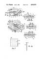
- FIGS. 6 and 6ashow another way of using the metal filled via holes provided on an alumina ceramic substrate in accordance with the present invention.
- an alumina substrate 65having a ground plane 82 on the bottom thereof, is shown provided with seven composite metal filled via holes 67, 68, 69, 70, 71, 72 and 73.
- the closely spaced metal filled via holes 67 and 68 on substrate 65have mounted over the tops thereof a single GaAs die 74 which provides a simplified hybrid microcircuit.
- the GaAs die 74has a primary ground 84 on the bottom thereof which directly contacts the metal fill in both the via holes 67 and 68 and that the bottoms of the metal fills in these via holes are in contact with the ground plane 82 on the bottom of the alumina substrate 65.
- the use of two metal filled via holes such as 67 and 68is needed when a GaAs die, such as die 74, generates heat faster than a single metal fill via hole can carry it away.
- the remaining five metal filled via holes 69-73 shown in FIG. 6are being used to provide for connection of terminals provided on the top of the GaAs die 74 to external circuits (not shown). It should be noted that the ground plane 82 on the bottom of alumina substrate 65 has enlarged holes about each of the five remaining metal filled via holes 69-73 to ensure that the metal fill of these via holes do not contact the ground plane 82.
- the metal filled via hole 69is connected by a ribbon lead 83 to the RF input terminal 75
- the metal filled via hole 70is connected by a ribbon lead 83 to the RF output terminal 76
- the metal filled via hole 71is connected by a ribbon lead 83 to the emitter terminal 77
- the metal filled via hole 72is connected by a ribbon lead 83 to the bias terminal 79
- the metal filled via hole 73is connected by a ribbon lead 83 to the drain terminal 78.
- the alumina substrate 65has a rectangularly configured thin-film metal pad 80 deposited about the border of its upper surface, as shown in FIG. 6. As shown in FIG.
- a metallic cover 81made of Kovar, for example, is placed over the alumina substrate 65 with its bottom sealed to the metal pad 80 so as to enclose the hybrid microwave circuit on the surface thereof.
- the metallic cover 81provides for shielding the hybrid microcircuit from outside interference.
- a pin 87is brazed on the bottom of each of the metal filled via holes 69-73 on the alumina substrate 65. These pins 87 are used for providing external connections for the terminals on the top of the GaAs die 74.
- a Cu/W block 85 which serves as a heat sinkis provided with five oversize through holes which are aligned with five metal filled via holes 69, 70, 71, 72, and 73 on the alumina substrate.
- FIGS. 6 and 6a of a single GaAs die 74 as a hybrid microcircuit on the alumina substrate 65is merely for illustrative purposes. More typically, several such GaAs dies, as well as other electronic components would be provided on the surface of the alumina substrate. Moreover, common terminals of several of these GaAs dies, for example, may be connected to the same metal filled via holes being used as external connectors.
Landscapes
- Engineering & Computer Science (AREA)
- Microelectronics & Electronic Packaging (AREA)
- Computer Hardware Design (AREA)
- Power Engineering (AREA)
- General Physics & Mathematics (AREA)
- Physics & Mathematics (AREA)
- Condensed Matter Physics & Semiconductors (AREA)
- Manufacturing & Machinery (AREA)
- Inorganic Chemistry (AREA)
- Chemical & Material Sciences (AREA)
- Ceramic Engineering (AREA)
- Cooling Or The Like Of Semiconductors Or Solid State Devices (AREA)
- Printing Elements For Providing Electric Connections Between Printed Circuits (AREA)
- Structure Of Printed Boards (AREA)
- Insulated Metal Substrates For Printed Circuits (AREA)
- Parts Printed On Printed Circuit Boards (AREA)
Abstract
Description
Claims (22)
Priority Applications (8)
| Application Number | Priority Date | Filing Date | Title |
|---|---|---|---|
| US07/266,669US4942076A (en) | 1988-11-03 | 1988-11-03 | Ceramic substrate with metal filled via holes for hybrid microcircuits and method of making the same |
| GB8924235AGB2226707B (en) | 1988-11-03 | 1989-10-27 | Ceramic substrate for hybrid microcircuits and method of making the same |
| FR8914311AFR2644964B1 (en) | 1988-11-03 | 1989-10-31 | CERAMIC SUBSTRATE WITH INTERCONNECTIONS BETWEEN METAL-FILLED LAYERS FOR HYBRID MICROCIRCUITS AND MANUFACTURING METHOD |
| IT02220389AIT1236637B (en) | 1988-11-03 | 1989-10-31 | CERAMIC SUBSTRATE WITH THROUGH HOLES FILLED WITH METAL FOR HYBRID MICROCIRCUITS AND PROCEDURE FOR MANUFACTURING THE SAME. |
| DE3936322ADE3936322C2 (en) | 1988-11-03 | 1989-11-01 | Method for producing a ceramic substrate with metal-filled through holes for a hybrid microcircuit and substrate produced in this way |
| CA002001982ACA2001982C (en) | 1988-11-03 | 1989-11-01 | Ceramic substrate with metal filled via holes for hybrid microcircuits and method of making the same |
| JP1285060AJPH07101724B2 (en) | 1988-11-03 | 1989-11-02 | Ceramic substrate having metal-filled through holes, method of manufacturing the same, hybrid microcircuit, and composite metal used for through holes |
| US07/543,096US5089881A (en) | 1988-11-03 | 1990-06-25 | Fine-pitch chip carrier |
Applications Claiming Priority (1)
| Application Number | Priority Date | Filing Date | Title |
|---|---|---|---|
| US07/266,669US4942076A (en) | 1988-11-03 | 1988-11-03 | Ceramic substrate with metal filled via holes for hybrid microcircuits and method of making the same |
Related Child Applications (1)
| Application Number | Title | Priority Date | Filing Date |
|---|---|---|---|
| US07/543,096Continuation-In-PartUS5089881A (en) | 1988-11-03 | 1990-06-25 | Fine-pitch chip carrier |
Publications (1)
| Publication Number | Publication Date |
|---|---|
| US4942076Atrue US4942076A (en) | 1990-07-17 |
Family
ID=23015518
Family Applications (1)
| Application Number | Title | Priority Date | Filing Date |
|---|---|---|---|
| US07/266,669Expired - LifetimeUS4942076A (en) | 1988-11-03 | 1988-11-03 | Ceramic substrate with metal filled via holes for hybrid microcircuits and method of making the same |
Country Status (7)
| Country | Link |
|---|---|
| US (1) | US4942076A (en) |
| JP (1) | JPH07101724B2 (en) |
| CA (1) | CA2001982C (en) |
| DE (1) | DE3936322C2 (en) |
| FR (1) | FR2644964B1 (en) |
| GB (1) | GB2226707B (en) |
| IT (1) | IT1236637B (en) |
Cited By (71)
| Publication number | Priority date | Publication date | Assignee | Title |
|---|---|---|---|---|
| US5089881A (en)* | 1988-11-03 | 1992-02-18 | Micro Substrates, Inc. | Fine-pitch chip carrier |
| US5221860A (en)* | 1991-02-19 | 1993-06-22 | At&T Bell Laboratories | High speed laser package |
| US5324570A (en)* | 1990-11-19 | 1994-06-28 | The Carborundum Company | Microelectronics package |
| US5325265A (en)* | 1988-11-10 | 1994-06-28 | Mcnc | High performance integrated circuit chip package |
| US5340947A (en)* | 1992-06-22 | 1994-08-23 | Cirqon Technologies Corporation | Ceramic substrates with highly conductive metal vias |
| US5552232A (en)* | 1994-12-21 | 1996-09-03 | International Business Machines Corporation | Aluminum nitride body having graded metallurgy |
| WO1996027282A1 (en)* | 1995-03-02 | 1996-09-06 | Circuit Components Incorporated | A low cost, high performance package for microwave circuits in the up to 90 ghz frequency range using bga i/o rf port format and ceramic substrate technology |
| US5614043A (en)* | 1992-09-17 | 1997-03-25 | Coors Ceramics Company | Method for fabricating electronic components incorporating ceramic-metal composites |
| US5624741A (en)* | 1990-05-31 | 1997-04-29 | E. I. Du Pont De Nemours And Company | Interconnect structure having electrical conduction paths formable therein |
| EP0755074A3 (en)* | 1995-07-18 | 1998-04-01 | Tokuyama Corporation | Submount |
| US5739586A (en)* | 1996-08-30 | 1998-04-14 | Scientific-Atlanta, Inc. | Heat sink assembly including a printed wiring board and a metal case |
| GB2325082A (en)* | 1997-05-08 | 1998-11-11 | Motorola Ltd | Thermal via arrangement |
| US5900675A (en)* | 1997-04-21 | 1999-05-04 | International Business Machines Corporation | Organic controlled collapse chip connector (C4) ball grid array (BGA) chip carrier with dual thermal expansion rates |
| US5930117A (en)* | 1996-05-07 | 1999-07-27 | Sheldahl, Inc. | Heat sink structure comprising a microarray of thermal metal heat channels or vias in a polymeric or film layer |
| US5963773A (en)* | 1997-06-14 | 1999-10-05 | Korea Institute Of Science And Technology | Tungsten skeleton structure fabrication method employed in application of copper infiltration and tungsten-copper composite material fabrication method thereof |
| US6037658A (en)* | 1997-10-07 | 2000-03-14 | International Business Machines Corporation | Electronic package with heat transfer means |
| US6049127A (en)* | 1997-06-14 | 2000-04-11 | Korea Institute Of Science And Technology | Hermetically sealed tungsten-copper composite package container for packaging of microwave devices |
| WO2000026942A3 (en)* | 1998-11-02 | 2000-08-31 | Coors Ceramics Company | Method for producing filled vias in electronic components |
| US6118671A (en)* | 1994-08-19 | 2000-09-12 | Hitachi, Ltd. | Circuit substrate and manufacture thereof, ceramic composition for circuit substrate, and electronics computer |
| US6143421A (en)* | 1992-09-17 | 2000-11-07 | Coorstek, Inc. | Electronic components incorporating ceramic-metal composites |
| US6338906B1 (en) | 1992-09-17 | 2002-01-15 | Coorstek, Inc. | Metal-infiltrated ceramic seal |
| US20020017855A1 (en)* | 1998-10-01 | 2002-02-14 | Complete Substrate Solutions Limited | Visual display |
| US6560121B1 (en)* | 1997-11-28 | 2003-05-06 | Thomson-Csf | Method for surface mounting of a microwave package on a printed circuit and package and printed circuit for implementing said method |
| EP1069811A3 (en)* | 1999-07-14 | 2003-05-07 | Nitto Denko Corporation | Multi-layer wiring board and method for manufacturing the same |
| US20030159772A1 (en)* | 2002-02-27 | 2003-08-28 | Optronx, Inc. | Method for improving heat dissipation in optical transmitter |
| US20030196825A1 (en)* | 2002-04-17 | 2003-10-23 | Richard Adams | Metal matrix composite structure and method |
| US6647039B2 (en) | 2002-02-27 | 2003-11-11 | Jds Uniphase Corporation | Reconfigurable laser header |
| US6646777B2 (en) | 2002-02-27 | 2003-11-11 | Jds Uniphase Corporation | Optical isolator with improved mounting characteristics |
| US6653557B2 (en) | 2002-02-27 | 2003-11-25 | Jds Uniphase Corporation | Faraday cage and ceramic walls for shielding EMI |
| US20040140521A1 (en)* | 2002-04-30 | 2004-07-22 | Hideki Okumura | Semiconductor device |
| RU2242823C2 (en)* | 1995-08-21 | 2004-12-20 | Открытое акционерное общество "НИИПП" | Method for producing microwave hybrid integrated circuits on ceramic substrates |
| US20050153534A1 (en)* | 2004-01-08 | 2005-07-14 | Shigeru Kikuchi | Electric contacts and method of manufacturing thereof, and vacuum interrupter and vacuum circuit breaker using thereof |
| US20060000591A1 (en)* | 2002-04-17 | 2006-01-05 | Adams Richard W | Metal matrix composite structure and method |
| US20060118945A1 (en)* | 2004-12-08 | 2006-06-08 | Ives Fred H | Low cost hermetic ceramic microcircuit package |
| US20060257631A1 (en)* | 2005-04-05 | 2006-11-16 | Chang Chi S | Probe pad structure in a ceramic space transformer |
| US20070007558A1 (en)* | 2005-06-27 | 2007-01-11 | Mazzochette Joseph B | Light emitting diode package and method for making same |
| US7349223B2 (en) | 2000-05-23 | 2008-03-25 | Nanonexus, Inc. | Enhanced compliant probe card systems having improved planarity |
| US7382142B2 (en) | 2000-05-23 | 2008-06-03 | Nanonexus, Inc. | High density interconnect system having rapid fabrication cycle |
| US7403029B2 (en) | 1999-05-27 | 2008-07-22 | Nanonexus Corporation | Massively parallel interface for electronic circuit |
| US20080242079A1 (en)* | 2007-03-30 | 2008-10-02 | Dingying Xu | In-situ formation of conductive filling material in through-silicon via |
| US20090188707A1 (en)* | 2008-01-30 | 2009-07-30 | Van Den Hoek Willibrordus Gerardus Maria | Method and Apparatus for Manufacture of Via Disk |
| US7579848B2 (en) | 2000-05-23 | 2009-08-25 | Nanonexus, Inc. | High density interconnect system for IC packages and interconnect assemblies |
| US20090256263A1 (en)* | 2008-04-09 | 2009-10-15 | International Business Machines Corporation | Structure and method for hybrid tungsten copper metal contact |
| US7621761B2 (en) | 2000-06-20 | 2009-11-24 | Nanonexus, Inc. | Systems for testing and packaging integrated circuits |
| US20100059865A1 (en)* | 2008-09-09 | 2010-03-11 | Lsi Corporation | Package with Power and Ground Through Via |
| US20100270062A1 (en)* | 2009-04-27 | 2010-10-28 | Ultrasource, Inc. | Method and Apparatus for an Improved Filled Via |
| US7847301B2 (en) | 2004-12-08 | 2010-12-07 | Agilent Technologies, Inc. | Electronic microcircuit having internal light enhancement |
| US7952373B2 (en) | 2000-05-23 | 2011-05-31 | Verigy (Singapore) Pte. Ltd. | Construction structures and manufacturing processes for integrated circuit wafer probe card assemblies |
| CN104064478A (en)* | 2014-06-24 | 2014-09-24 | 南京航空航天大学 | A kind of manufacturing method of copper/aluminum nitride ceramic composite heat conduction substrate |
| US20150216051A1 (en)* | 2011-12-21 | 2015-07-30 | Lawrence Livermore National Security, Llc | Method of fabricating electrical feedthroughs using extruded metal vias |
| CN105489559A (en)* | 2015-11-30 | 2016-04-13 | 中国电子科技集团公司第五十五研究所 | Aluminium nitride substrate for microwave power tube and manufacturing method therefor |
| EP2942808A4 (en)* | 2013-01-07 | 2016-11-16 | Almt Corp | CERAMIC WIRING SUBSTRATE, SEMICONDUCTOR DEVICE, AND METHOD FOR MANUFACTURING CERAMIC WIRING SUBSTRATE |
| US20180061666A1 (en)* | 2016-08-29 | 2018-03-01 | Infineon Technologies Ag | Method for Producing a Metal-Ceramic Substrate with at Least One Via |
| US10185191B2 (en) | 2016-08-02 | 2019-01-22 | Omnivision Technologies, Inc. | Panel carrier and method for attaching a liquid-crystal-on-silicon panel thereto |
| WO2020139957A1 (en)* | 2018-12-28 | 2020-07-02 | 3D Glass Solutions, Inc. | Planar substrate and metal interface for rf, microwave and mm wave systems |
| US10854946B2 (en) | 2017-12-15 | 2020-12-01 | 3D Glass Solutions, Inc. | Coupled transmission line resonate RF filter |
| US10903545B2 (en) | 2018-05-29 | 2021-01-26 | 3D Glass Solutions, Inc. | Method of making a mechanically stabilized radio frequency transmission line device |
| US11076489B2 (en) | 2018-04-10 | 2021-07-27 | 3D Glass Solutions, Inc. | RF integrated power condition capacitor |
| US11101532B2 (en) | 2017-04-28 | 2021-08-24 | 3D Glass Solutions, Inc. | RF circulator |
| US11139582B2 (en) | 2018-09-17 | 2021-10-05 | 3D Glass Solutions, Inc. | High efficiency compact slotted antenna with a ground plane |
| US11161773B2 (en) | 2016-04-08 | 2021-11-02 | 3D Glass Solutions, Inc. | Methods of fabricating photosensitive substrates suitable for optical coupler |
| US11264167B2 (en) | 2016-02-25 | 2022-03-01 | 3D Glass Solutions, Inc. | 3D capacitor and capacitor array fabricating photoactive substrates |
| US11270843B2 (en) | 2018-12-28 | 2022-03-08 | 3D Glass Solutions, Inc. | Annular capacitor RF, microwave and MM wave systems |
| US11342896B2 (en) | 2017-07-07 | 2022-05-24 | 3D Glass Solutions, Inc. | 2D and 3D RF lumped element devices for RF system in a package photoactive glass substrates |
| US11373908B2 (en) | 2019-04-18 | 2022-06-28 | 3D Glass Solutions, Inc. | High efficiency die dicing and release |
| US11594457B2 (en) | 2018-12-28 | 2023-02-28 | 3D Glass Solutions, Inc. | Heterogenous integration for RF, microwave and MM wave systems in photoactive glass substrates |
| US11677373B2 (en) | 2018-01-04 | 2023-06-13 | 3D Glass Solutions, Inc. | Impedence matching conductive structure for high efficiency RF circuits |
| US11908617B2 (en) | 2020-04-17 | 2024-02-20 | 3D Glass Solutions, Inc. | Broadband induction |
| US11929199B2 (en) | 2014-05-05 | 2024-03-12 | 3D Glass Solutions, Inc. | 2D and 3D inductors fabricating photoactive substrates |
| US11962057B2 (en) | 2019-04-05 | 2024-04-16 | 3D Glass Solutions, Inc. | Glass based empty substrate integrated waveguide devices |
| US12165809B2 (en) | 2016-02-25 | 2024-12-10 | 3D Glass Solutions, Inc. | 3D capacitor and capacitor array fabricating photoactive substrates |
Families Citing this family (9)
| Publication number | Priority date | Publication date | Assignee | Title |
|---|---|---|---|---|
| DE3931634A1 (en)* | 1989-09-22 | 1991-04-04 | Telefunken Electronic Gmbh | SEMICONDUCTOR COMPONENT |
| FR2663159B1 (en)* | 1990-06-12 | 1997-01-24 | Thomson Hybrides | SYSTEM FOR HERMETICALLY CONDITIONING A HYBRID MODULE. |
| DE4103294C2 (en)* | 1991-02-04 | 2000-12-28 | Altan Akyuerek | Process for the production of ceramic printed circuit boards with vias |
| DE4130925A1 (en)* | 1991-09-17 | 1993-03-18 | Telefunken Systemtechnik | CARRIER FOR PLANAR MICROWAVE CIRCUITS |
| DE4201612C2 (en)* | 1992-01-22 | 1996-07-18 | Alf Harnisch | Process for the galvanic introduction of metal and alloy into structured glass or glass ceramic bodies and use of the process for the production of metal composites |
| GB9219661D0 (en)* | 1992-09-17 | 1992-10-28 | Oxley Dev Company Limited | Ceramic microwave packages |
| GB2290171B (en) | 1994-06-03 | 1998-01-21 | Plessey Semiconductors Ltd | Inductor chip device |
| US6301122B1 (en)* | 1996-06-13 | 2001-10-09 | Matsushita Electric Industrial Co., Ltd. | Radio frequency module with thermally and electrically coupled metal film on insulating substrate |
| DE102020201868A1 (en)* | 2020-02-14 | 2021-08-19 | Robert Bosch Gesellschaft mit beschränkter Haftung | Circuit carrier with a thermally conductive printed metal inlay |
Citations (10)
| Publication number | Priority date | Publication date | Assignee | Title |
|---|---|---|---|---|
| US3045331A (en)* | 1959-06-26 | 1962-07-24 | Mallory & Co Inc P R | Electrical contacts of high arc erosion resistance and method of making the same |
| US3628999A (en)* | 1970-03-05 | 1971-12-21 | Frederick W Schneble Jr | Plated through hole printed circuit boards |
| US4131516A (en)* | 1977-07-21 | 1978-12-26 | International Business Machines Corporation | Method of making metal filled via holes in ceramic circuit boards |
| US4394712A (en)* | 1981-03-18 | 1983-07-19 | General Electric Company | Alignment-enhancing feed-through conductors for stackable silicon-on-sapphire wafers |
| US4435611A (en)* | 1980-03-24 | 1984-03-06 | Sony Corporation | Conductive paste |
| US4540604A (en)* | 1983-08-25 | 1985-09-10 | E. I. Du Pont De Nemours And Company | Thick film conductor compositions |
| US4712161A (en)* | 1985-03-25 | 1987-12-08 | Olin Corporation | Hybrid and multi-layer circuitry |
| US4732780A (en)* | 1985-09-26 | 1988-03-22 | General Electric Company | Method of making hermetic feedthrough in ceramic substrate |
| US4788523A (en)* | 1987-12-10 | 1988-11-29 | United States Of America | Viad chip resistor |
| US4835039A (en)* | 1986-11-26 | 1989-05-30 | Ceramics Process Systems Corporation | Tungsten paste for co-sintering with pure alumina and method for producing same |
Family Cites Families (21)
| Publication number | Priority date | Publication date | Assignee | Title |
|---|---|---|---|---|
| GB1372901A (en)* | 1971-12-02 | 1974-11-06 | Ibm | Electrical interconnection structure |
| GB1485569A (en)* | 1974-09-10 | 1977-09-14 | Siemens Ag | Multi-layer wired substrates for multi-chip circuits |
| JPS5651846A (en)* | 1979-10-04 | 1981-05-09 | Fujitsu Ltd | Ic package |
| US4437109A (en)* | 1980-11-07 | 1984-03-13 | General Electric Company | Silicon-on-sapphire body with conductive paths therethrough |
| FR2525815B1 (en)* | 1982-04-27 | 1985-08-30 | Inf Milit Spatiale Aeronaut | COMPOSITE SUBSTRATE WITH HIGH THERMAL CONDUCTION AND APPLICATION TO SEMICONDUCTOR DEVICE HOUSINGS |
| JPS5921032A (en)* | 1982-07-26 | 1984-02-02 | Sumitomo Electric Ind Ltd | Substrate for semiconductor device |
| JPS5946050A (en)* | 1982-09-09 | 1984-03-15 | Narumi China Corp | Ceramic package for semiconductor |
| JPS5954247A (en)* | 1982-09-21 | 1984-03-29 | Nec Corp | Electronic component parts |
| GB2136210B (en)* | 1983-02-14 | 1987-09-23 | Raymond E Wiech | Method of forming substrates |
| JPS60502282A (en)* | 1983-09-21 | 1985-12-26 | アライド コ−ポレイシヨン | Printed circuit board manufacturing method |
| US4519760A (en)* | 1984-04-02 | 1985-05-28 | Burroughs Corporation | Machine for filling via holes in an integrated circuit package with conductive ink |
| US4521449A (en)* | 1984-05-21 | 1985-06-04 | International Business Machines Corporation | Process for forming a high density metallurgy system on a substrate and structure thereof |
| JPS61182247A (en)* | 1985-02-08 | 1986-08-14 | Nippon Telegr & Teleph Corp <Ntt> | Ic package |
| GB8526397D0 (en)* | 1985-10-25 | 1985-11-27 | Oxley Dev Co Ltd | Metallising paste |
| DE3777856D1 (en)* | 1986-02-24 | 1992-05-07 | Hewlett Packard Co | HERMETIC, MICROELECTRONIC HIGH FREQUENCY PACK FOR SURFACE MOUNTING. |
| GB2188194A (en)* | 1986-03-21 | 1987-09-23 | Plessey Co Plc | Carrier for high frequency integrated circuits |
| JPS62174341U (en)* | 1986-04-25 | 1987-11-05 | ||
| US4922324A (en)* | 1987-01-20 | 1990-05-01 | Kabushiki Kaisha Toshiba | Semiconductor integrated circuit device |
| JPS6413755A (en)* | 1987-01-20 | 1989-01-18 | Toshiba Corp | Semiconductor integrated circuit device |
| US4880684A (en)* | 1988-03-11 | 1989-11-14 | International Business Machines Corporation | Sealing and stress relief layers and use thereof |
| US4925723A (en)* | 1988-09-29 | 1990-05-15 | Microwave Power, Inc. | Microwave integrated circuit substrate including metal filled via holes and method of manufacture |
- 1988
- 1988-11-03USUS07/266,669patent/US4942076A/ennot_activeExpired - Lifetime
- 1989
- 1989-10-27GBGB8924235Apatent/GB2226707B/ennot_activeExpired - Fee Related
- 1989-10-31ITIT02220389Apatent/IT1236637B/enactiveIP Right Grant
- 1989-10-31FRFR8914311Apatent/FR2644964B1/ennot_activeExpired - Fee Related
- 1989-11-01DEDE3936322Apatent/DE3936322C2/ennot_activeExpired - Fee Related
- 1989-11-01CACA002001982Apatent/CA2001982C/ennot_activeExpired - Fee Related
- 1989-11-02JPJP1285060Apatent/JPH07101724B2/ennot_activeExpired - Fee Related
Patent Citations (10)
| Publication number | Priority date | Publication date | Assignee | Title |
|---|---|---|---|---|
| US3045331A (en)* | 1959-06-26 | 1962-07-24 | Mallory & Co Inc P R | Electrical contacts of high arc erosion resistance and method of making the same |
| US3628999A (en)* | 1970-03-05 | 1971-12-21 | Frederick W Schneble Jr | Plated through hole printed circuit boards |
| US4131516A (en)* | 1977-07-21 | 1978-12-26 | International Business Machines Corporation | Method of making metal filled via holes in ceramic circuit boards |
| US4435611A (en)* | 1980-03-24 | 1984-03-06 | Sony Corporation | Conductive paste |
| US4394712A (en)* | 1981-03-18 | 1983-07-19 | General Electric Company | Alignment-enhancing feed-through conductors for stackable silicon-on-sapphire wafers |
| US4540604A (en)* | 1983-08-25 | 1985-09-10 | E. I. Du Pont De Nemours And Company | Thick film conductor compositions |
| US4712161A (en)* | 1985-03-25 | 1987-12-08 | Olin Corporation | Hybrid and multi-layer circuitry |
| US4732780A (en)* | 1985-09-26 | 1988-03-22 | General Electric Company | Method of making hermetic feedthrough in ceramic substrate |
| US4835039A (en)* | 1986-11-26 | 1989-05-30 | Ceramics Process Systems Corporation | Tungsten paste for co-sintering with pure alumina and method for producing same |
| US4788523A (en)* | 1987-12-10 | 1988-11-29 | United States Of America | Viad chip resistor |
Cited By (101)
| Publication number | Priority date | Publication date | Assignee | Title |
|---|---|---|---|---|
| US5089881A (en)* | 1988-11-03 | 1992-02-18 | Micro Substrates, Inc. | Fine-pitch chip carrier |
| US5325265A (en)* | 1988-11-10 | 1994-06-28 | Mcnc | High performance integrated circuit chip package |
| US5624741A (en)* | 1990-05-31 | 1997-04-29 | E. I. Du Pont De Nemours And Company | Interconnect structure having electrical conduction paths formable therein |
| US5324570A (en)* | 1990-11-19 | 1994-06-28 | The Carborundum Company | Microelectronics package |
| US5221860A (en)* | 1991-02-19 | 1993-06-22 | At&T Bell Laboratories | High speed laser package |
| US5340947A (en)* | 1992-06-22 | 1994-08-23 | Cirqon Technologies Corporation | Ceramic substrates with highly conductive metal vias |
| US6143421A (en)* | 1992-09-17 | 2000-11-07 | Coorstek, Inc. | Electronic components incorporating ceramic-metal composites |
| US5614043A (en)* | 1992-09-17 | 1997-03-25 | Coors Ceramics Company | Method for fabricating electronic components incorporating ceramic-metal composites |
| US6338906B1 (en) | 1992-09-17 | 2002-01-15 | Coorstek, Inc. | Metal-infiltrated ceramic seal |
| US6346317B1 (en) | 1992-09-17 | 2002-02-12 | Coorstek, Inc. | Electronic components incorporating ceramic-metal composites |
| US6118671A (en)* | 1994-08-19 | 2000-09-12 | Hitachi, Ltd. | Circuit substrate and manufacture thereof, ceramic composition for circuit substrate, and electronics computer |
| US5552232A (en)* | 1994-12-21 | 1996-09-03 | International Business Machines Corporation | Aluminum nitride body having graded metallurgy |
| US5552107A (en)* | 1994-12-21 | 1996-09-03 | Ibm | Aluminum nitride body having graded metallurgy |
| US5682589A (en)* | 1994-12-21 | 1997-10-28 | International Business Machines Corporation | Aluminum nitride body having graded metallurgy |
| US5763093A (en)* | 1994-12-21 | 1998-06-09 | International Business Machines Corporation | Aluminum nitride body having graded metallurgy |
| WO1996027282A1 (en)* | 1995-03-02 | 1996-09-06 | Circuit Components Incorporated | A low cost, high performance package for microwave circuits in the up to 90 ghz frequency range using bga i/o rf port format and ceramic substrate technology |
| EP0755074A3 (en)* | 1995-07-18 | 1998-04-01 | Tokuyama Corporation | Submount |
| US5770821A (en)* | 1995-07-18 | 1998-06-23 | Tokuyama Corporation | Submount |
| RU2242823C2 (en)* | 1995-08-21 | 2004-12-20 | Открытое акционерное общество "НИИПП" | Method for producing microwave hybrid integrated circuits on ceramic substrates |
| US5930117A (en)* | 1996-05-07 | 1999-07-27 | Sheldahl, Inc. | Heat sink structure comprising a microarray of thermal metal heat channels or vias in a polymeric or film layer |
| US5930601A (en)* | 1996-08-30 | 1999-07-27 | Scientific-Atlanta, Inc. | Heat assembly and method of transferring heat |
| US5739586A (en)* | 1996-08-30 | 1998-04-14 | Scientific-Atlanta, Inc. | Heat sink assembly including a printed wiring board and a metal case |
| US5900675A (en)* | 1997-04-21 | 1999-05-04 | International Business Machines Corporation | Organic controlled collapse chip connector (C4) ball grid array (BGA) chip carrier with dual thermal expansion rates |
| GB2325082A (en)* | 1997-05-08 | 1998-11-11 | Motorola Ltd | Thermal via arrangement |
| US6049127A (en)* | 1997-06-14 | 2000-04-11 | Korea Institute Of Science And Technology | Hermetically sealed tungsten-copper composite package container for packaging of microwave devices |
| US5963773A (en)* | 1997-06-14 | 1999-10-05 | Korea Institute Of Science And Technology | Tungsten skeleton structure fabrication method employed in application of copper infiltration and tungsten-copper composite material fabrication method thereof |
| US6037658A (en)* | 1997-10-07 | 2000-03-14 | International Business Machines Corporation | Electronic package with heat transfer means |
| US6560121B1 (en)* | 1997-11-28 | 2003-05-06 | Thomson-Csf | Method for surface mounting of a microwave package on a printed circuit and package and printed circuit for implementing said method |
| US20020017855A1 (en)* | 1998-10-01 | 2002-02-14 | Complete Substrate Solutions Limited | Visual display |
| US6270601B1 (en) | 1998-11-02 | 2001-08-07 | Coorstek, Inc. | Method for producing filled vias in electronic components |
| WO2000026942A3 (en)* | 1998-11-02 | 2000-08-31 | Coors Ceramics Company | Method for producing filled vias in electronic components |
| US7884634B2 (en) | 1999-05-27 | 2011-02-08 | Verigy (Singapore) Pte, Ltd | High density interconnect system having rapid fabrication cycle |
| US7772860B2 (en) | 1999-05-27 | 2010-08-10 | Nanonexus, Inc. | Massively parallel interface for electronic circuit |
| US7403029B2 (en) | 1999-05-27 | 2008-07-22 | Nanonexus Corporation | Massively parallel interface for electronic circuit |
| EP1069811A3 (en)* | 1999-07-14 | 2003-05-07 | Nitto Denko Corporation | Multi-layer wiring board and method for manufacturing the same |
| US7382142B2 (en) | 2000-05-23 | 2008-06-03 | Nanonexus, Inc. | High density interconnect system having rapid fabrication cycle |
| US7952373B2 (en) | 2000-05-23 | 2011-05-31 | Verigy (Singapore) Pte. Ltd. | Construction structures and manufacturing processes for integrated circuit wafer probe card assemblies |
| US7872482B2 (en) | 2000-05-23 | 2011-01-18 | Verigy (Singapore) Pte. Ltd | High density interconnect system having rapid fabrication cycle |
| US7579848B2 (en) | 2000-05-23 | 2009-08-25 | Nanonexus, Inc. | High density interconnect system for IC packages and interconnect assemblies |
| US7349223B2 (en) | 2000-05-23 | 2008-03-25 | Nanonexus, Inc. | Enhanced compliant probe card systems having improved planarity |
| US7621761B2 (en) | 2000-06-20 | 2009-11-24 | Nanonexus, Inc. | Systems for testing and packaging integrated circuits |
| US6653557B2 (en) | 2002-02-27 | 2003-11-25 | Jds Uniphase Corporation | Faraday cage and ceramic walls for shielding EMI |
| US6646777B2 (en) | 2002-02-27 | 2003-11-11 | Jds Uniphase Corporation | Optical isolator with improved mounting characteristics |
| US6773532B2 (en) | 2002-02-27 | 2004-08-10 | Jds Uniphase Corporation | Method for improving heat dissipation in optical transmitter |
| US20030159772A1 (en)* | 2002-02-27 | 2003-08-28 | Optronx, Inc. | Method for improving heat dissipation in optical transmitter |
| US6647039B2 (en) | 2002-02-27 | 2003-11-11 | Jds Uniphase Corporation | Reconfigurable laser header |
| US20030196825A1 (en)* | 2002-04-17 | 2003-10-23 | Richard Adams | Metal matrix composite structure and method |
| US7141310B2 (en)* | 2002-04-17 | 2006-11-28 | Ceramics Process Systems Corporation | Metal matrix composite structure and method |
| US20060000591A1 (en)* | 2002-04-17 | 2006-01-05 | Adams Richard W | Metal matrix composite structure and method |
| US6884522B2 (en) | 2002-04-17 | 2005-04-26 | Ceramics Process Systems Corp. | Metal matrix composite structure and method |
| US7262477B2 (en)* | 2002-04-30 | 2007-08-28 | Kabushiki Kaisha Toshiba | Semiconductor device |
| US20040140521A1 (en)* | 2002-04-30 | 2004-07-22 | Hideki Okumura | Semiconductor device |
| US20050153534A1 (en)* | 2004-01-08 | 2005-07-14 | Shigeru Kikuchi | Electric contacts and method of manufacturing thereof, and vacuum interrupter and vacuum circuit breaker using thereof |
| US7230304B2 (en)* | 2004-01-08 | 2007-06-12 | Hitachi, Ltd. | Electric contacts and method of manufacturing thereof, and vacuum interrupter and vacuum circuit breaker using thereof |
| US20060118945A1 (en)* | 2004-12-08 | 2006-06-08 | Ives Fred H | Low cost hermetic ceramic microcircuit package |
| US7847301B2 (en) | 2004-12-08 | 2010-12-07 | Agilent Technologies, Inc. | Electronic microcircuit having internal light enhancement |
| US7821129B2 (en) | 2004-12-08 | 2010-10-26 | Agilent Technologies, Inc. | Low cost hermetic ceramic microcircuit package |
| US7374811B2 (en)* | 2005-04-05 | 2008-05-20 | Sv Probe Pte Ltd. | Probe pad structure in a ceramic space transformer |
| US20060257631A1 (en)* | 2005-04-05 | 2006-11-16 | Chang Chi S | Probe pad structure in a ceramic space transformer |
| US20070007558A1 (en)* | 2005-06-27 | 2007-01-11 | Mazzochette Joseph B | Light emitting diode package and method for making same |
| US20080242079A1 (en)* | 2007-03-30 | 2008-10-02 | Dingying Xu | In-situ formation of conductive filling material in through-silicon via |
| US7851342B2 (en)* | 2007-03-30 | 2010-12-14 | Intel Corporation | In-situ formation of conductive filling material in through-silicon via |
| US8242382B2 (en) | 2008-01-30 | 2012-08-14 | Innovent Technologies, Llc | Method and apparatus for manufacture of via disk |
| US20090188707A1 (en)* | 2008-01-30 | 2009-07-30 | Van Den Hoek Willibrordus Gerardus Maria | Method and Apparatus for Manufacture of Via Disk |
| WO2009097489A1 (en) | 2008-01-30 | 2009-08-06 | Innovent Technologies, Llc | Method and apparatus for manufacture of via disk |
| US7629264B2 (en) | 2008-04-09 | 2009-12-08 | International Business Machines Corporation | Structure and method for hybrid tungsten copper metal contact |
| US20090256263A1 (en)* | 2008-04-09 | 2009-10-15 | International Business Machines Corporation | Structure and method for hybrid tungsten copper metal contact |
| US20100059865A1 (en)* | 2008-09-09 | 2010-03-11 | Lsi Corporation | Package with Power and Ground Through Via |
| US20100270062A1 (en)* | 2009-04-27 | 2010-10-28 | Ultrasource, Inc. | Method and Apparatus for an Improved Filled Via |
| US8362368B2 (en) | 2009-04-27 | 2013-01-29 | Ultrasource, Inc. | Method and apparatus for an improved filled via |
| EP2796018A4 (en)* | 2011-12-21 | 2015-08-12 | Satinderpall S Pannu | Method of fabricating electrical feedthroughs using extruded metal vias |
| US20150216051A1 (en)* | 2011-12-21 | 2015-07-30 | Lawrence Livermore National Security, Llc | Method of fabricating electrical feedthroughs using extruded metal vias |
| EP2942808A4 (en)* | 2013-01-07 | 2016-11-16 | Almt Corp | CERAMIC WIRING SUBSTRATE, SEMICONDUCTOR DEVICE, AND METHOD FOR MANUFACTURING CERAMIC WIRING SUBSTRATE |
| US11929199B2 (en) | 2014-05-05 | 2024-03-12 | 3D Glass Solutions, Inc. | 2D and 3D inductors fabricating photoactive substrates |
| CN104064478B (en)* | 2014-06-24 | 2016-08-31 | 南京航空航天大学 | A kind of manufacture method of copper/aluminium nitride ceramics composite heat-conducting substrate |
| CN104064478A (en)* | 2014-06-24 | 2014-09-24 | 南京航空航天大学 | A kind of manufacturing method of copper/aluminum nitride ceramic composite heat conduction substrate |
| CN105489559A (en)* | 2015-11-30 | 2016-04-13 | 中国电子科技集团公司第五十五研究所 | Aluminium nitride substrate for microwave power tube and manufacturing method therefor |
| CN105489559B (en)* | 2015-11-30 | 2018-01-16 | 中国电子科技集团公司第五十五研究所 | A kind of effective aluminium nitride substrate of microwave power and its manufacture method |
| US12165809B2 (en) | 2016-02-25 | 2024-12-10 | 3D Glass Solutions, Inc. | 3D capacitor and capacitor array fabricating photoactive substrates |
| US11264167B2 (en) | 2016-02-25 | 2022-03-01 | 3D Glass Solutions, Inc. | 3D capacitor and capacitor array fabricating photoactive substrates |
| US11161773B2 (en) | 2016-04-08 | 2021-11-02 | 3D Glass Solutions, Inc. | Methods of fabricating photosensitive substrates suitable for optical coupler |
| US10185191B2 (en) | 2016-08-02 | 2019-01-22 | Omnivision Technologies, Inc. | Panel carrier and method for attaching a liquid-crystal-on-silicon panel thereto |
| US20180061666A1 (en)* | 2016-08-29 | 2018-03-01 | Infineon Technologies Ag | Method for Producing a Metal-Ceramic Substrate with at Least One Via |
| US11804383B2 (en) | 2016-08-29 | 2023-10-31 | Infineon Technologies Ag | Method for producing a metal-ceramic substrate with electrically conductive vias |
| US11557490B2 (en)* | 2016-08-29 | 2023-01-17 | Infineon Technologies Ag | Method for producing a metal-ceramic substrate with at least one via |
| US10796929B2 (en)* | 2016-08-29 | 2020-10-06 | Infineon Technologies Ag | Method for producing a metal-ceramic substrate with at least one via |
| US11101532B2 (en) | 2017-04-28 | 2021-08-24 | 3D Glass Solutions, Inc. | RF circulator |
| US11342896B2 (en) | 2017-07-07 | 2022-05-24 | 3D Glass Solutions, Inc. | 2D and 3D RF lumped element devices for RF system in a package photoactive glass substrates |
| US10854946B2 (en) | 2017-12-15 | 2020-12-01 | 3D Glass Solutions, Inc. | Coupled transmission line resonate RF filter |
| US11367939B2 (en) | 2017-12-15 | 2022-06-21 | 3D Glass Solutions, Inc. | Coupled transmission line resonate RF filter |
| US11894594B2 (en) | 2017-12-15 | 2024-02-06 | 3D Glass Solutions, Inc. | Coupled transmission line resonate RF filter |
| US11677373B2 (en) | 2018-01-04 | 2023-06-13 | 3D Glass Solutions, Inc. | Impedence matching conductive structure for high efficiency RF circuits |
| US11076489B2 (en) | 2018-04-10 | 2021-07-27 | 3D Glass Solutions, Inc. | RF integrated power condition capacitor |
| US10903545B2 (en) | 2018-05-29 | 2021-01-26 | 3D Glass Solutions, Inc. | Method of making a mechanically stabilized radio frequency transmission line device |
| US11139582B2 (en) | 2018-09-17 | 2021-10-05 | 3D Glass Solutions, Inc. | High efficiency compact slotted antenna with a ground plane |
| US11270843B2 (en) | 2018-12-28 | 2022-03-08 | 3D Glass Solutions, Inc. | Annular capacitor RF, microwave and MM wave systems |
| US11594457B2 (en) | 2018-12-28 | 2023-02-28 | 3D Glass Solutions, Inc. | Heterogenous integration for RF, microwave and MM wave systems in photoactive glass substrates |
| WO2020139957A1 (en)* | 2018-12-28 | 2020-07-02 | 3D Glass Solutions, Inc. | Planar substrate and metal interface for rf, microwave and mm wave systems |
| US11962057B2 (en) | 2019-04-05 | 2024-04-16 | 3D Glass Solutions, Inc. | Glass based empty substrate integrated waveguide devices |
| US11373908B2 (en) | 2019-04-18 | 2022-06-28 | 3D Glass Solutions, Inc. | High efficiency die dicing and release |
| US11908617B2 (en) | 2020-04-17 | 2024-02-20 | 3D Glass Solutions, Inc. | Broadband induction |
Also Published As
| Publication number | Publication date |
|---|---|
| DE3936322C2 (en) | 1997-04-30 |
| JPH07101724B2 (en) | 1995-11-01 |
| GB2226707A (en) | 1990-07-04 |
| GB2226707B (en) | 1993-05-26 |
| FR2644964B1 (en) | 1994-03-25 |
| CA2001982C (en) | 1995-02-07 |
| JPH02216853A (en) | 1990-08-29 |
| DE3936322A1 (en) | 1990-05-10 |
| IT8922203A0 (en) | 1989-10-31 |
| CA2001982A1 (en) | 1990-05-03 |
| IT1236637B (en) | 1993-03-25 |
| IT8922203A1 (en) | 1991-05-01 |
| FR2644964A1 (en) | 1990-09-28 |
| GB8924235D0 (en) | 1989-12-13 |
Similar Documents
| Publication | Publication Date | Title |
|---|---|---|
| US4942076A (en) | Ceramic substrate with metal filled via holes for hybrid microcircuits and method of making the same | |
| US4925024A (en) | Hermetic high frequency surface mount microelectronic package | |
| KR100367936B1 (en) | High frequency integrated circuit device with laminated body | |
| EP0115000B1 (en) | Power chip package | |
| US5043796A (en) | Isolating multiple device mount with stress relief | |
| US3753056A (en) | Microwave semiconductor device | |
| US4736273A (en) | Power semiconductor device for surface mounting | |
| EP0235503B1 (en) | Hermetic high frequency surface mount microelectronic package | |
| JPH0613726A (en) | Ceramics circuit board | |
| JPH01168045A (en) | hermetically sealed circuit device | |
| JPH0368157A (en) | High frequency thick film integrated circuit device | |
| JPH0677631A (en) | Mounting method of chip component onto aluminum board | |
| JPH06163765A (en) | Aluminum nitride heat sink and its manufacture | |
| JP3323171B2 (en) | Package for storing semiconductor elements | |
| KR102735483B1 (en) | Ceramic substrate unit and manufacturing method thereof | |
| US5324570A (en) | Microelectronics package | |
| JP2000164996A (en) | Ceramic wiring board | |
| JPH06260566A (en) | Land grid array package, its manufacture and semiconductor package | |
| JPS6016749B2 (en) | Packages for integrated circuits | |
| JPH0746007A (en) | Power board and high frequency power amplifier | |
| JPH05299532A (en) | Method for manufacturing aluminum nitride multilayer circuit board | |
| JPH03283641A (en) | Ceramic package | |
| JPH0287558A (en) | Ic chip | |
| JPH0272696A (en) | ceramic circuit board | |
| JP2515672Y2 (en) | Package for storing semiconductor devices |
Legal Events
| Date | Code | Title | Description |
|---|---|---|---|
| AS | Assignment | Owner name:MICRO STRATES, INC., A CA CORP., CALIFORNIA Free format text:ASSIGNMENT OF ASSIGNORS INTEREST.;ASSIGNORS:PANICKER, RAMACHANDRA M. P.;AGARWAL, ANIL K.;REEL/FRAME:005020/0542;SIGNING DATES FROM 19890201 TO 19890207 | |
| STCF | Information on status: patent grant | Free format text:PATENTED CASE | |
| AS | Assignment | Owner name:MICRO SUBSTRATES, INC., CALIFORNIA Free format text:ASSIGNMENT OF ASSIGNORS INTEREST.;ASSIGNOR:MICRO STRATES, INC., A CORP. OF CA.;REEL/FRAME:005381/0260 Effective date:19900428 | |
| AS | Assignment | Owner name:MICRO SUBSTRATES INC., AN ARIZONA CORP., ARIZONA Free format text:ASSIGNMENT OF ASSIGNORS INTEREST.;ASSIGNOR:MICRO SUBSTRATES, INC. A CALIFORNIA CORP.;REEL/FRAME:006315/0301 Effective date:19921003 | |
| FEPP | Fee payment procedure | Free format text:PAT HLDR NO LONGER CLAIMS SMALL ENT STAT AS SMALL BUSINESS (ORIGINAL EVENT CODE: LSM2); ENTITY STATUS OF PATENT OWNER: LARGE ENTITY | |
| REFU | Refund | Free format text:REFUND PROCESSED. MAINTENANCE FEE HAS ALREADY BEEN PAID (ORIGINAL EVENT CODE: R160); ENTITY STATUS OF PATENT OWNER: LARGE ENTITY | |
| FPAY | Fee payment | Year of fee payment:4 | |
| AS | Assignment | Owner name:MICRO SUBSTRATES CORPORATION, A AZ CORP. Free format text:CHANGE OF NAME;ASSIGNOR:MICRO SUBSTRATES, INC., A AZ CORP.;REEL/FRAME:007410/0379 Effective date:19930215 | |
| FEPP | Fee payment procedure | Free format text:PAYOR NUMBER ASSIGNED (ORIGINAL EVENT CODE: ASPN); ENTITY STATUS OF PATENT OWNER: LARGE ENTITY | |
| FPAY | Fee payment | Year of fee payment:8 | |
| FPAY | Fee payment | Year of fee payment:12 | |
| REMI | Maintenance fee reminder mailed |