US4933910A - Method for improving the page hit ratio of a page mode main memory system - Google Patents
Method for improving the page hit ratio of a page mode main memory systemDownload PDFInfo
- Publication number
- US4933910A US4933910AUS07/215,652US21565288AUS4933910AUS 4933910 AUS4933910 AUS 4933910AUS 21565288 AUS21565288 AUS 21565288AUS 4933910 AUS4933910 AUS 4933910A
- Authority
- US
- United States
- Prior art keywords
- cycle
- memory
- access
- page
- page mode
- Prior art date
- Legal status (The legal status is an assumption and is not a legal conclusion. Google has not performed a legal analysis and makes no representation as to the accuracy of the status listed.)
- Expired - Lifetime
Links
- 238000000034methodMethods0.000titleclaimsdescription24
- 230000004044responseEffects0.000claimsdescription4
- 230000000977initiatory effectEffects0.000claimsdescription3
- 238000010586diagramMethods0.000description5
- 240000007320Pinus strobusSpecies0.000description4
- 230000007704transitionEffects0.000description4
- 230000008901benefitEffects0.000description2
- 238000012986modificationMethods0.000description2
- 230000004048modificationEffects0.000description2
- 230000004075alterationEffects0.000description1
- 230000007812deficiencyEffects0.000description1
- 230000000694effectsEffects0.000description1
- 230000000415inactivating effectEffects0.000description1
- 230000007257malfunctionEffects0.000description1
Images

Classifications
- G—PHYSICS
- G11—INFORMATION STORAGE
- G11C—STATIC STORES
- G11C7/00—Arrangements for writing information into, or reading information out from, a digital store
- G11C7/10—Input/output [I/O] data interface arrangements, e.g. I/O data control circuits, I/O data buffers
- G11C7/1015—Read-write modes for single port memories, i.e. having either a random port or a serial port
- G11C7/1018—Serial bit line access mode, e.g. using bit line address shift registers, bit line address counters, bit line burst counters
- G11C7/1021—Page serial bit line access mode, i.e. using an enabled row address stroke pulse with its associated word line address and a sequence of enabled column address stroke pulses each with its associated bit line address
Definitions
- the present inventionrelates generally to methods of accessing main memory in a computer system. More particularly, the present invention relates to a page mode method of accessing main memory. Specifically, the present invention provides a method whereby a page mode memory access can occur despite an immediately previous idle cycle.
- main memoryIn high speed computer systems, main memory is used to store all information required by the current working set. It has been found that accessing main memory information in a page mode fashion can partially overcome the typical slow access speed of main memory. The reason for this is that a page mode access enjoys a shorter cycle time than a conventional memory access, thus allowing the memory system to more quickly respond to a CPU request.
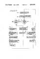
- FIG. 1is a general block diagram illustrating a computer system having the capability to make page mode main memory accesses
- FIG. 2is a flow chart representing a method of page mode main memory access which could be used with the computer system of FIG. 1;
- FIG. 3is a state diagram representing a prior art method of carrying out the page mode main memory access method of FIG. 2;
- FIG. 4is a state diagram representing the method of the present invention of carrying out the method of page mode memory access of FIG. 2.
- the present inventionaccomplishes the above and other objects through a method of page mode main memory access which takes into account whether the current cycle is an idle cycle. If it is determined that the current cycle is an idle cycle, then the state of certain page mode hardware is preserved during the idle cycle. By preserving the state of page mode hardware during the idle cycle, any subsequent main memory access may be carried out via the page mode.
- a CPU 10communicates with a memory array 12 via a data bus 14 and an address bus 16.
- Memory array 12may be main memory of the computer system consisting of dynamic random access memory (DRAM) devices.
- DRAMdynamic random access memory
- the computer system shown in FIG. 1has the capability to access memory array 12 in either a conventional manner or in a page mode fashion.
- Memory array 12is architecturally organized as an array of rows and columns wherein any element of memory array 12 can be identified by selecting a particular row and a particular column.
- address informationthe high order address information found on address bus 16 is used to select a particular row, and the low order address information likewise corresponds to a particular column.
- a latch 20is provided to receive high order address lines of address bus 16 and temporarily store the information present on those lines during a main memory access cycle. This latched information represents the row selected during that memory access cycle.
- An address comparator 22compares current high order address, or row, information to the latched row information of the previous memory cycle and outputs, at 24, whether a match exists.
- a page memory controller 26responds to the output 24 of address comparator 22 and a signal 28 generated by CPU 10 indicating the start of a memory access, and outputs memory control signals MEMPAGE 30 and MEMCYCLE 32.
- a local memory controller 34is then provided to receive MEMPAGE 30 and MEMCYCLE 32 and generate in response thereto a row address strobe (RAS) 36 signal and a column address strobe (CAS) 38 signal.
- RASrow address strobe
- CAScolumn address strobe
- RAS 36goes active when the information on memory address bus 40 corresponds to the high order, or row, address information of address bus 16 during a memory access cycle.
- CAS 38goes active when the information on memory address bus 40 corresponds to the low order, or column, address information of address bus 16 during a memory access cycle.
- Multiplexer 42is provided so that the information on memory address bus 40 can be switched between either high order address, or row, information, shown at 44, or low order address, or column, information, shown at 46.
- RAS 36When RAS 36 is activated, it strobes row address information present on the memory address bus 40 into memory array 12. After this, multiplexer 42 is switched so that column address information 46 is placed on the memory address bus 40.
- CAS 38is activated to strobe the column address information into memory array 12. In this way, any element of memory array 12 can be accessed via its unique row and column combination.
- the CPUemits the address of the requested memory access on the address bus.
- the high order, or row, information of this addressis compared to the high order, or row, information of the previous memory cycle.
- a decisionis made as to whether the row addresses match and RAS is active. RAS being active indicates that the current cycle is an access to main memory, and an address match indicates that the row selected during the previous cycle is the same as the row now being selected in the current cycle.
- a conventional access to main memorymust be executed. This is accomplished by first inactivating MEMPAGE and MEMCYCLE, at block 62, which causes the local memory controller to inactivate both RAS and CAS. Next, at block 64, the latch laches current row address information for future comparison with the row address information of the next memory access cycle. Then, at block 66, the system must wait for a defined amount of time, known as the RAS precharge time. After the RAS precharge time has elapsed, the page memory controller activates MEMPAGE which in turn causes RAS to go active strobing the row address information into the memory array.
- the multiplexeris switched so that the column address information appears on the memory address bus, and after it becomes valid, the page memory controller activates MEMCYCLE, which in turn causes CAS to go active strobing the column address information into the memory array.
- the memory arrayhas both the row information and the column information needed to access the requested memory element, and at block 70, the system waits until the memory array responds and the cycle is completed before returning to block 50.
- the page memory controllerinactivates MEMCYCLE which causes CAS to go inactive. RAS remains active at this time.
- the latchlatches current row information for future comparison with the row address information of the next memory access cycle.
- the systemmust wait for a definite amount of time, known as the CAS precharge time, for the column address information on the memory address bus supplied by the multiplexer to become valid.
- the page memory controlleractivates MEMCYCLE which in turn causes CAS to go active strobing the column address information into the memory array.
- the memory arrayhas both the row information and the column information needed to access the requested memory element, and at block 78, the system waits until the memory array responds and the cycle is completed before returning to block 50.
- a state diagramillustrates a prior art method of carrying out the page mode method of FIG. 2.
- the state machineenters state 100 and remains there until a memory cycle occurs.
- RAS and CASare held inactive.
- the state machineproceeds to state 101 where RAS becomes active. It then proceeds to state 102 where CAS becomes active in addition to RAS being active.
- state 103is reached where RAS and CAS remain active. The state machine remains in state 103 until the next cycle is initiated.
- a subsequent cycleis a memory access cycle and also happens to be a "page hit" (i.e., if the row address emitted by the CPU during this cycle is the same as the row address emitted by the CPU during the most recent previous memory access cycle)
- controlpasses to state 101 for a write cycle or to state 102 for a read cycle.
- Transition 104causes CAS to go inactive, but at the first clock pulse after control passes to state 101 for a write cycle or state 102 for a read cycle, CAS again goes active. The period during which CAS is inactive is the CAS precharge time described above. At this point, the state machine progresses as before to state 103 where it again remains until the next cycle is initiated.
- a page mode memory accesscan be significantly shorter than a conventional access by virtue of there being no need to wait for the RAS precharge time to elapse.
- the occurrence of an idle cyclewill not transfer control to state 100 of FIG. 3 but will result in control remaining in state 103 so that if a subsequent cycle happens to be a page hit, then quick page mode accessing can occur.
- idle cyclesare treated as extensions of a previous cycle.
- a subsequent cyclehappens to access the same page, or row, of memory as the most recent cycle previous to the idle cycle or cycles, it can be carried out in page mode fashion.
- the present methodis implemented in a manner whereby memory control logic keeps RAS active during idle cycles. Thus, if a page hit is detected on a subsequent cycle, a page mode access is performed since RAS is already active and all that is needed to read or write to the memory is CAS. If any cycle other than a page hit is detected, RAS goes inactive and the requested operation is executed in the usual manner.
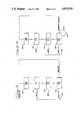
- FIG. 4illustrates a state diagram of the method of the present invention.
- the state machineremains in state 120 until a memory cycle occurs.
- RAS and CASare held inactive.
- controlpasses to state 121 where RAS becomes active.
- the machinethen proceeds to state 122 where CAS becomes active in addition to RAS being active.
- State 123is finally reached where RAS and CAS remain active and where the machine remains until the next cycle is initiated.
- Transition 124causes CAS to go inactive which is the beginning of CAS precharge, but CAS again goes active at the next clock pulse, strobing column address information into memory. The state machine again progresses to state 123 where it again waits until a subsequent cycle begins.
- controlonly returns to state 120 if that cycle is also not an idle cycle, as shown at transition 125. If it is an idle cycle, control remains at state 123 until the next cycle is initiated, as shown at transition 126. In this manner, an idle cycle does not return control to state 120 where a conventional access must next be forced, but rather leaves control at state 123 where a subsequent page mode access is still possible.
- a method for allowing a page mode access to occur immediately following one or more idle cyclesis disclosed.
- an idle cyclewill no longer force a slow conventional access on the next memory cycle.
- RASis maintained active during idle cycles despite the CPU being forced out of its pipelined addressing mode. In this way, a subsequent page mode access is possible.
- other cyclessuch as direct memory access cycles or interrupt cycles, which may cause the contents of the previous cycle row address latch to become mismatched with the actual row address information strobed into memory
- idle cyclesdo not have this effect.
- system performancecan be improved without the risk of malfunction from the possibility of a mismatch as described above.
Landscapes
- Dram (AREA)
- Memory System (AREA)
Abstract
Description
Claims (3)
Priority Applications (1)
| Application Number | Priority Date | Filing Date | Title |
|---|---|---|---|
| US07/215,652US4933910A (en) | 1988-07-06 | 1988-07-06 | Method for improving the page hit ratio of a page mode main memory system |
Applications Claiming Priority (1)
| Application Number | Priority Date | Filing Date | Title |
|---|---|---|---|
| US07/215,652US4933910A (en) | 1988-07-06 | 1988-07-06 | Method for improving the page hit ratio of a page mode main memory system |
Publications (1)
| Publication Number | Publication Date |
|---|---|
| US4933910Atrue US4933910A (en) | 1990-06-12 |
Family
ID=22803836
Family Applications (1)
| Application Number | Title | Priority Date | Filing Date |
|---|---|---|---|
| US07/215,652Expired - LifetimeUS4933910A (en) | 1988-07-06 | 1988-07-06 | Method for improving the page hit ratio of a page mode main memory system |
Country Status (1)
| Country | Link |
|---|---|
| US (1) | US4933910A (en) |
Cited By (40)
| Publication number | Priority date | Publication date | Assignee | Title |
|---|---|---|---|---|
| US5159676A (en)* | 1988-12-05 | 1992-10-27 | Micron Technology, Inc. | Semi-smart DRAM controller IC to provide a pseudo-cache mode of operation using standard page mode draws |
| US5185720A (en)* | 1990-12-07 | 1993-02-09 | Trw Inc. | Memory module for use in a large reconfigurable memory |
| US5202857A (en)* | 1990-11-07 | 1993-04-13 | Emc Corporation | System for generating memory timing and reducing memory access time |
| US5241510A (en)* | 1991-01-11 | 1993-08-31 | Kabushiki Kaisha Toshiba | Semiconductor integrated circuit |
| US5253214A (en)* | 1991-09-27 | 1993-10-12 | Eastman Kodak Company | High-performance memory controller with application-programmable optimization |
| US5262991A (en)* | 1991-11-22 | 1993-11-16 | Zilog, Inc. | Device with multiplexed and non-multiplexed address and data I/O capability |
| US5265236A (en)* | 1990-11-29 | 1993-11-23 | Sun Microsystems, Inc. | Method and apparatus for increasing the speed of memory access in a virtual memory system having fast page mode |
| US5276856A (en)* | 1989-09-28 | 1994-01-04 | Pixel Semiconductor, Inc. | Memory controller flexible timing control system and method |
| US5282177A (en)* | 1992-04-08 | 1994-01-25 | Micron Technology, Inc. | Multiple register block write method and circuit for video DRAMs |
| US5303364A (en)* | 1989-09-29 | 1994-04-12 | Compaq Computer Corp. | Paged memory controller |
| US5335336A (en)* | 1988-03-28 | 1994-08-02 | Hitachi, Ltd. | Memory device having refresh mode returning previous page address for resumed page mode |
| US5436869A (en)* | 1993-07-08 | 1995-07-25 | Nec Corporation | Memory controller which can carry out a high speed access when supplied with input addresses with a time interval left between the input addresses having the same row address |
| US5493666A (en)* | 1990-03-19 | 1996-02-20 | Apple Computer, Inc. | Memory architecture using page mode writes and single level write buffering |
| US5524228A (en)* | 1990-04-26 | 1996-06-04 | Fuji Xerox Co., Ltd. | Memory control circuit for reducing the number of row address signals |
| US5566318A (en)* | 1994-08-02 | 1996-10-15 | Ramtron International Corporation | Circuit with a single address register that augments a memory controller by enabling cache reads and page-mode writes |
| US5604883A (en)* | 1990-08-06 | 1997-02-18 | Ncr Corporation | Computer memory open page bias method and system |
| US5634112A (en)* | 1994-10-14 | 1997-05-27 | Compaq Computer Corporation | Memory controller having precharge prediction based on processor and PCI bus cycles |
| US5644747A (en)* | 1994-03-08 | 1997-07-01 | Nec Corporation | Page mode access memory controller including plural address latches and a comparator |
| US5657288A (en)* | 1994-04-13 | 1997-08-12 | Ericsson Inc. | Efficient addressing of large memories |
| US5724540A (en)* | 1988-03-28 | 1998-03-03 | Hitachi, Ltd. | Memory system having a column address counter and a page address counter |
| US5771369A (en)* | 1990-08-31 | 1998-06-23 | International Business Machines Corporation | Memory row redrive |
| US5835945A (en)* | 1990-08-06 | 1998-11-10 | Ncr Corporation | Memory system with write buffer, prefetch and internal caches |
| US5850368A (en)* | 1995-06-01 | 1998-12-15 | Micron Technology, Inc. | Burst EDO memory address counter |
| US5940848A (en)* | 1997-01-14 | 1999-08-17 | Intel Corporation | Computer system and method for efficiently controlling the opening and closing of pages for an aborted row on page miss cycle |
| US5946265A (en)* | 1995-12-14 | 1999-08-31 | Micron Technology, Inc. | Continuous burst EDO memory device |
| US6052756A (en)* | 1998-01-23 | 2000-04-18 | Oki Electric Industry Co., Ltd. | Memory page management |
| US6272608B1 (en)* | 1997-07-10 | 2001-08-07 | Micron Technology, Inc. | Method and apparatus for synchronous data transfers in a memory device with lookahead logic for detecting latency intervals |
| US6381180B1 (en) | 1994-12-23 | 2002-04-30 | Micron Technology, Inc. | Distributed write data drivers for burst access memories |
| US6405280B1 (en) | 1998-06-05 | 2002-06-11 | Micron Technology, Inc. | Packet-oriented synchronous DRAM interface supporting a plurality of orderings for data block transfers within a burst sequence |
| US6519719B1 (en) | 1997-06-13 | 2003-02-11 | Micron Technology, Inc. | Method and apparatus for transferring test data from a memory array |
| US6525971B2 (en) | 1995-06-30 | 2003-02-25 | Micron Technology, Inc. | Distributed write data drivers for burst access memories |
| US6601156B2 (en) | 1996-07-03 | 2003-07-29 | Micron Technology, Inc. | Continuous interleave burst access |
| US6615325B2 (en) | 1996-01-11 | 2003-09-02 | Micron Technology, Inc. | Method for switching between modes of operation |
| US6981126B1 (en) | 1996-07-03 | 2005-12-27 | Micron Technology, Inc. | Continuous interleave burst access |
| US20060039213A1 (en)* | 1990-04-18 | 2006-02-23 | Rambus Inc. | Integrated circuit I/O using a high performance bus interface |
| US20060291587A1 (en)* | 1997-06-20 | 2006-12-28 | Massachusetts Institute Of Technology | Digital transmitter |
| US20080043546A1 (en)* | 1995-10-19 | 2008-02-21 | Rambus Inc. | Method of Controlling A Memory Device Having a Memory Core |
| US7646654B2 (en) | 1994-12-23 | 2010-01-12 | Micron Technology, Inc. | Distributed write data drivers for burst access memories |
| US8501563B2 (en) | 2005-07-20 | 2013-08-06 | Micron Technology, Inc. | Devices with nanocrystals and methods of formation |
| US9583334B2 (en) | 2006-01-10 | 2017-02-28 | Micron Technology, Inc. | Gallium lanthanide oxide films |
Citations (4)
| Publication number | Priority date | Publication date | Assignee | Title |
|---|---|---|---|---|
| US4535428A (en)* | 1983-03-10 | 1985-08-13 | International Business Machines Corporation | Multi-port register implementations |
| US4596004A (en)* | 1983-09-14 | 1986-06-17 | International Business Machines Corporation | High speed memory with a multiplexed address bus |
| US4750839A (en)* | 1985-08-07 | 1988-06-14 | Texas Instruments Incorporated | Semiconductor memory with static column decode and page mode addressing capability |
| US4792929A (en)* | 1987-03-23 | 1988-12-20 | Zenith Electronics Corporation | Data processing system with extended memory access |
- 1988
- 1988-07-06USUS07/215,652patent/US4933910A/ennot_activeExpired - Lifetime
Patent Citations (4)
| Publication number | Priority date | Publication date | Assignee | Title |
|---|---|---|---|---|
| US4535428A (en)* | 1983-03-10 | 1985-08-13 | International Business Machines Corporation | Multi-port register implementations |
| US4596004A (en)* | 1983-09-14 | 1986-06-17 | International Business Machines Corporation | High speed memory with a multiplexed address bus |
| US4750839A (en)* | 1985-08-07 | 1988-06-14 | Texas Instruments Incorporated | Semiconductor memory with static column decode and page mode addressing capability |
| US4792929A (en)* | 1987-03-23 | 1988-12-20 | Zenith Electronics Corporation | Data processing system with extended memory access |
Cited By (80)
| Publication number | Priority date | Publication date | Assignee | Title |
|---|---|---|---|---|
| US5724540A (en)* | 1988-03-28 | 1998-03-03 | Hitachi, Ltd. | Memory system having a column address counter and a page address counter |
| US5479635A (en)* | 1988-03-28 | 1995-12-26 | Hitachi, Ltd. | Memory device including DRAMs for high-speed accessing |
| US5335336A (en)* | 1988-03-28 | 1994-08-02 | Hitachi, Ltd. | Memory device having refresh mode returning previous page address for resumed page mode |
| US5159676A (en)* | 1988-12-05 | 1992-10-27 | Micron Technology, Inc. | Semi-smart DRAM controller IC to provide a pseudo-cache mode of operation using standard page mode draws |
| US5276856A (en)* | 1989-09-28 | 1994-01-04 | Pixel Semiconductor, Inc. | Memory controller flexible timing control system and method |
| US5303364A (en)* | 1989-09-29 | 1994-04-12 | Compaq Computer Corp. | Paged memory controller |
| US5493666A (en)* | 1990-03-19 | 1996-02-20 | Apple Computer, Inc. | Memory architecture using page mode writes and single level write buffering |
| US7209997B2 (en) | 1990-04-18 | 2007-04-24 | Rambus Inc. | Controller device and method for operating same |
| US20060039213A1 (en)* | 1990-04-18 | 2006-02-23 | Rambus Inc. | Integrated circuit I/O using a high performance bus interface |
| US5524228A (en)* | 1990-04-26 | 1996-06-04 | Fuji Xerox Co., Ltd. | Memory control circuit for reducing the number of row address signals |
| US5604883A (en)* | 1990-08-06 | 1997-02-18 | Ncr Corporation | Computer memory open page bias method and system |
| US5835945A (en)* | 1990-08-06 | 1998-11-10 | Ncr Corporation | Memory system with write buffer, prefetch and internal caches |
| US5771369A (en)* | 1990-08-31 | 1998-06-23 | International Business Machines Corporation | Memory row redrive |
| US5202857A (en)* | 1990-11-07 | 1993-04-13 | Emc Corporation | System for generating memory timing and reducing memory access time |
| US5265236A (en)* | 1990-11-29 | 1993-11-23 | Sun Microsystems, Inc. | Method and apparatus for increasing the speed of memory access in a virtual memory system having fast page mode |
| US5185720A (en)* | 1990-12-07 | 1993-02-09 | Trw Inc. | Memory module for use in a large reconfigurable memory |
| US5241510A (en)* | 1991-01-11 | 1993-08-31 | Kabushiki Kaisha Toshiba | Semiconductor integrated circuit |
| US5253214A (en)* | 1991-09-27 | 1993-10-12 | Eastman Kodak Company | High-performance memory controller with application-programmable optimization |
| US5293562A (en)* | 1991-11-22 | 1994-03-08 | Zilog, Inc. | Device with multiplexed and non-multiplexed address and data I/O capability |
| US5262991A (en)* | 1991-11-22 | 1993-11-16 | Zilog, Inc. | Device with multiplexed and non-multiplexed address and data I/O capability |
| US5282177A (en)* | 1992-04-08 | 1994-01-25 | Micron Technology, Inc. | Multiple register block write method and circuit for video DRAMs |
| US5436869A (en)* | 1993-07-08 | 1995-07-25 | Nec Corporation | Memory controller which can carry out a high speed access when supplied with input addresses with a time interval left between the input addresses having the same row address |
| US5644747A (en)* | 1994-03-08 | 1997-07-01 | Nec Corporation | Page mode access memory controller including plural address latches and a comparator |
| US5657288A (en)* | 1994-04-13 | 1997-08-12 | Ericsson Inc. | Efficient addressing of large memories |
| US5680567A (en)* | 1994-04-13 | 1997-10-21 | Ericsson Inc. | Efficient addressing of large memories |
| US5566318A (en)* | 1994-08-02 | 1996-10-15 | Ramtron International Corporation | Circuit with a single address register that augments a memory controller by enabling cache reads and page-mode writes |
| US5960459A (en)* | 1994-10-14 | 1999-09-28 | Compaq Computer Corporation | Memory controller having precharge prediction based on processor and PCI bus cycles |
| US5634112A (en)* | 1994-10-14 | 1997-05-27 | Compaq Computer Corporation | Memory controller having precharge prediction based on processor and PCI bus cycles |
| US5813038A (en)* | 1994-10-14 | 1998-09-22 | Compaq Computer Corporation | Memory controller having precharge prediction based on processor and PC bus cycles |
| US6381180B1 (en) | 1994-12-23 | 2002-04-30 | Micron Technology, Inc. | Distributed write data drivers for burst access memories |
| US8213244B2 (en) | 1994-12-23 | 2012-07-03 | Round Rock Research, Llc | Distributed write data drivers for burst access memories |
| US8107304B2 (en) | 1994-12-23 | 2012-01-31 | Round Rock Research, Llc | Distributed write data drivers for burst access memories |
| US7075857B2 (en) | 1994-12-23 | 2006-07-11 | Micron Technology, Inc. | Distributed write data drivers for burst access memories |
| US7646654B2 (en) | 1994-12-23 | 2010-01-12 | Micron Technology, Inc. | Distributed write data drivers for burst access memories |
| US7088625B2 (en) | 1994-12-23 | 2006-08-08 | Micron Technology, Inc. | Distributed write data drivers for burst access memories |
| US20060198180A1 (en)* | 1994-12-23 | 2006-09-07 | Micron Technology, Inc. | Distributed write data drivers for burst access memories |
| US6914830B2 (en) | 1994-12-23 | 2005-07-05 | Micron Technology, Inc. | Distributed write data drivers for burst access memories |
| US7397711B2 (en) | 1994-12-23 | 2008-07-08 | Micron Technology, Inc. | Distributed write data drivers for burst access memories |
| US20050036367A1 (en)* | 1994-12-23 | 2005-02-17 | Micron Technology, Inc. | Distributed write data drivers for burst access memories |
| US6728142B2 (en) | 1994-12-23 | 2004-04-27 | Micron Technology, Inc. | Distributed write data drivers for burst access memories |
| US5850368A (en)* | 1995-06-01 | 1998-12-15 | Micron Technology, Inc. | Burst EDO memory address counter |
| US6525971B2 (en) | 1995-06-30 | 2003-02-25 | Micron Technology, Inc. | Distributed write data drivers for burst access memories |
| US20080043546A1 (en)* | 1995-10-19 | 2008-02-21 | Rambus Inc. | Method of Controlling A Memory Device Having a Memory Core |
| US5946265A (en)* | 1995-12-14 | 1999-08-31 | Micron Technology, Inc. | Continuous burst EDO memory device |
| US20070239956A1 (en)* | 1996-01-11 | 2007-10-11 | Micron Technology, Inc. | Asynchronously-accessible memory devices and access methods |
| US6615325B2 (en) | 1996-01-11 | 2003-09-02 | Micron Technology, Inc. | Method for switching between modes of operation |
| US6601156B2 (en) | 1996-07-03 | 2003-07-29 | Micron Technology, Inc. | Continuous interleave burst access |
| US7210020B2 (en) | 1996-07-03 | 2007-04-24 | Micron Technology, Inc. | Continuous interleave burst access |
| US6981126B1 (en) | 1996-07-03 | 2005-12-27 | Micron Technology, Inc. | Continuous interleave burst access |
| US20060064540A1 (en)* | 1996-07-03 | 2006-03-23 | Micron Technology, Inc. | Continuous interleave burst access |
| US5940848A (en)* | 1997-01-14 | 1999-08-17 | Intel Corporation | Computer system and method for efficiently controlling the opening and closing of pages for an aborted row on page miss cycle |
| US6519719B1 (en) | 1997-06-13 | 2003-02-11 | Micron Technology, Inc. | Method and apparatus for transferring test data from a memory array |
| US20090262794A1 (en)* | 1997-06-20 | 2009-10-22 | Massachusetts Institute Of Technology | Digital transmitter |
| US20060291587A1 (en)* | 1997-06-20 | 2006-12-28 | Massachusetts Institute Of Technology | Digital transmitter |
| US9647857B2 (en) | 1997-06-20 | 2017-05-09 | Massachusetts Institute Of Technology | Digital transmitter |
| US9419824B2 (en) | 1997-06-20 | 2016-08-16 | Massachusetts Institute Of Technology | Digital transmitter |
| US8989303B2 (en) | 1997-06-20 | 2015-03-24 | Massachusetts Institute Of Technology | Digital transmitter |
| US8923433B2 (en) | 1997-06-20 | 2014-12-30 | Massachusetts Institute Of Technology | Digital transmitter |
| US8761235B2 (en) | 1997-06-20 | 2014-06-24 | Massachusetts Institute Of Technology | Digital transmitter |
| US8254491B2 (en) | 1997-06-20 | 2012-08-28 | Massachusetts Institute Of Technology | Digital transmitter |
| US8681837B2 (en) | 1997-06-20 | 2014-03-25 | Massachusetts Institute Of Technology | Digital Transmitter |
| US20100034252A1 (en)* | 1997-06-20 | 2010-02-11 | Dally William J | Digital Transmitter |
| US20110051794A1 (en)* | 1997-06-20 | 2011-03-03 | Massachusetts Institute Of Technology | Digital Transmitter |
| US8311147B2 (en) | 1997-06-20 | 2012-11-13 | Massachusetts Institute Of Technology | Digital transmitter |
| US8259841B2 (en) | 1997-06-20 | 2012-09-04 | Massachusetts Institute Of Technology | Digital transmitter |
| US8238467B2 (en) | 1997-06-20 | 2012-08-07 | Massachusetts Institute Of Technology | Digital transmitter |
| US8238470B2 (en) | 1997-06-20 | 2012-08-07 | Massachusetts Institute Of Technology | Digital transmitter |
| US8243847B2 (en) | 1997-06-20 | 2012-08-14 | Massachusetts Institute Of Technology | Digital transmitter |
| US6415340B1 (en) | 1997-07-10 | 2002-07-02 | Micron Technology, Inc. | Method and apparatus for synchronous data transfers in a memory device with selectable data or address paths |
| US6272608B1 (en)* | 1997-07-10 | 2001-08-07 | Micron Technology, Inc. | Method and apparatus for synchronous data transfers in a memory device with lookahead logic for detecting latency intervals |
| US6556483B2 (en) | 1997-07-10 | 2003-04-29 | Micron Technology, Inc. | Method and apparatus for synchronous data transfers in a memory device with selectable data or address paths |
| US6560668B2 (en) | 1997-07-10 | 2003-05-06 | Micron Technology, Inc. | Method and apparatus for reading write-modified read data in memory device providing synchronous data transfers |
| US6611885B2 (en) | 1997-07-10 | 2003-08-26 | Micron Technology, Inc. | Method and apparatus for synchronous data transfers in a memory device with selectable data or address paths |
| US6614698B2 (en) | 1997-07-10 | 2003-09-02 | Micron Technology, Inc. | Method and apparatus for synchronous data transfers in a memory device with selectable data or address paths |
| US6789175B2 (en) | 1997-07-10 | 2004-09-07 | Micron Technology, Inc. | Method and apparatus for synchronous data transfers in a memory device with selectable data or address paths |
| US6052756A (en)* | 1998-01-23 | 2000-04-18 | Oki Electric Industry Co., Ltd. | Memory page management |
| US6405280B1 (en) | 1998-06-05 | 2002-06-11 | Micron Technology, Inc. | Packet-oriented synchronous DRAM interface supporting a plurality of orderings for data block transfers within a burst sequence |
| US8501563B2 (en) | 2005-07-20 | 2013-08-06 | Micron Technology, Inc. | Devices with nanocrystals and methods of formation |
| US8921914B2 (en) | 2005-07-20 | 2014-12-30 | Micron Technology, Inc. | Devices with nanocrystals and methods of formation |
| US9583334B2 (en) | 2006-01-10 | 2017-02-28 | Micron Technology, Inc. | Gallium lanthanide oxide films |
Similar Documents
| Publication | Publication Date | Title |
|---|---|---|
| US4933910A (en) | Method for improving the page hit ratio of a page mode main memory system | |
| US4847758A (en) | Main memory access in a microprocessor system with a cache memory | |
| US5889714A (en) | Adaptive precharge management for synchronous DRAM | |
| US6526471B1 (en) | Method and apparatus for a high-speed memory subsystem | |
| US6046953A (en) | Decoded autorefresh mode in a DRAM | |
| EP0375121B1 (en) | Method and apparatus for efficient DRAM control | |
| US5687183A (en) | Memory access system with overwrite prevention for overlapping write operations | |
| US20030217223A1 (en) | Combined command set | |
| EP1579335B1 (en) | Read-write switching method for a memory controller | |
| JPH0471223B2 (en) | ||
| US6505282B1 (en) | Method and apparatus for determining memory types of a multi-type memory subsystem where memory of the different types are accessed using column control signals with different timing characteristics | |
| US5627988A (en) | Data memories and method for storing multiple categories of data in latches dedicated to particular category | |
| US20080098176A1 (en) | Method and Apparatus for Implementing Memory Accesses Using Open Page Mode for Data Prefetching | |
| US6128716A (en) | Memory controller with continuous page mode and method therefor | |
| US6252794B1 (en) | DRAM and data access method for DRAM | |
| US5513143A (en) | Data cache memory internal circuitry for reducing wait states | |
| US6026466A (en) | Multiple row address strobe DRAM architecture to improve bandwidth | |
| US5893917A (en) | Memory controller and method of closing a page of system memory | |
| US6373769B1 (en) | Decoded autofresh mode in a DRAM | |
| US5644747A (en) | Page mode access memory controller including plural address latches and a comparator | |
| US5771369A (en) | Memory row redrive | |
| US5577218A (en) | Memory access control method wherein block access is performed as a sequential access to an address updated by incrementation | |
| US5479640A (en) | Memory access system including a memory controller with memory redrive circuitry | |
| EP0607668B1 (en) | Electronic memory system and method | |
| US5940848A (en) | Computer system and method for efficiently controlling the opening and closing of pages for an aborted row on page miss cycle |
Legal Events
| Date | Code | Title | Description |
|---|---|---|---|
| AS | Assignment | Owner name:ZENITH DATA SYSTEMS CORPORATION, MICHIGAN Free format text:ASSIGNMENT OF ASSIGNORS INTEREST.;ASSIGNOR:ZENITH ELECTRONICS CORPORATION;REEL/FRAME:005203/0471 Effective date:19891228 | |
| STCF | Information on status: patent grant | Free format text:PATENTED CASE | |
| AS | Assignment | Owner name:ZENITH DATA SYSTEMS CORPORATION, MICHIGAN Free format text:ASSIGNMENT OF ASSIGNORS INTEREST.;ASSIGNOR:ZENITH ELECTRONICS CORPORATION;REEL/FRAME:005800/0568 Effective date:19910311 | |
| FEPP | Fee payment procedure | Free format text:PAYOR NUMBER ASSIGNED (ORIGINAL EVENT CODE: ASPN); ENTITY STATUS OF PATENT OWNER: LARGE ENTITY | |
| FPAY | Fee payment | Year of fee payment:4 | |
| AS | Assignment | Owner name:ZENITH DATA SYSTEMS CORPORATION, ILLINOIS Free format text:ASSIGNMENT OF ASSIGNORS INTEREST;ASSIGNORS:OLSON, ANTHONY M.;RAJARAM, BABU;ROBINSON, THOMAS N.;REEL/FRAME:007062/0561 Effective date:19880701 | |
| REMI | Maintenance fee reminder mailed | ||
| FPAY | Fee payment | Year of fee payment:8 | |
| SULP | Surcharge for late payment | ||
| AS | Assignment | Owner name:PACKARD BELL NEC, INC., CALIFORNIA Free format text:MERGER;ASSIGNOR:ZENITH DATA SYSTEMS CORPORATION;REEL/FRAME:009245/0518 Effective date:19970320 | |
| AS | Assignment | Owner name:SUMITOMO BANK OF NEW YORK TRUST COMPANY, NEW YORK Free format text:SECURITY INTEREST;ASSIGNOR:PACKARD BELL NEC, INC.;REEL/FRAME:009479/0358 Effective date:19970325 | |
| FEPP | Fee payment procedure | Free format text:PAYER NUMBER DE-ASSIGNED (ORIGINAL EVENT CODE: RMPN); ENTITY STATUS OF PATENT OWNER: LARGE ENTITY Free format text:PAYOR NUMBER ASSIGNED (ORIGINAL EVENT CODE: ASPN); ENTITY STATUS OF PATENT OWNER: LARGE ENTITY | |
| AS | Assignment | Owner name:SUMITOMO BANK, THE, LIMITED, NEW YORK BRANCH, AS C Free format text:TRANSFER OF SECURITY INTEREST;ASSIGNOR:SUMITOMO BANK OF NEW YORK TRUST COMPANY;REEL/FRAME:009748/0570 Effective date:19990217 | |
| AS | Assignment | Owner name:PACKARD BELL NEC, INC., CALIFORNIA Free format text:TERMINATION OF SECURITY INTEREST;ASSIGNOR:SUMITOMO BANK LIMITED, THE, NEW YORK BRANCH, AS COLLATERAL AGENT FOR LENDER;REEL/FRAME:010231/0935 Effective date:19990301 | |
| AS | Assignment | Owner name:NEC CORPORATION, JAPAN Free format text:ASSIGNMENT OF ASSIGNORS INTEREST;ASSIGNOR:PACKARD BELL NEC, INC.;REEL/FRAME:011007/0153 Effective date:20000223 | |
| FPAY | Fee payment | Year of fee payment:12 | |
| SULP | Surcharge for late payment | Year of fee payment:11 | |
| REMI | Maintenance fee reminder mailed |