US4933845A - Reconfigurable bus - Google Patents
Reconfigurable busDownload PDFInfo
- Publication number
- US4933845A US4933845AUS07/093,200US9320087AUS4933845AUS 4933845 AUS4933845 AUS 4933845AUS 9320087 AUS9320087 AUS 9320087AUS 4933845 AUS4933845 AUS 4933845A
- Authority
- US
- United States
- Prior art keywords
- bus
- processor
- memory
- type
- input
- Prior art date
- Legal status (The legal status is an assumption and is not a legal conclusion. Google has not performed a legal analysis and makes no representation as to the accuracy of the status listed.)
- Expired - Lifetime
Links
Images


Classifications
- G—PHYSICS
- G06—COMPUTING OR CALCULATING; COUNTING
- G06F—ELECTRIC DIGITAL DATA PROCESSING
- G06F13/00—Interconnection of, or transfer of information or other signals between, memories, input/output devices or central processing units
- G06F13/38—Information transfer, e.g. on bus
- G06F13/40—Bus structure
- G—PHYSICS
- G06—COMPUTING OR CALCULATING; COUNTING
- G06F—ELECTRIC DIGITAL DATA PROCESSING
- G06F15/00—Digital computers in general; Data processing equipment in general
- G06F15/16—Combinations of two or more digital computers each having at least an arithmetic unit, a program unit and a register, e.g. for a simultaneous processing of several programs
- G06F15/177—Initialisation or configuration control
Definitions
- This inventionrelates to data processing in general and more particularly, to a reconfigurable bus for use in a data processing system, which bus can be configured to either communicate with external memory or external I/O such as an additional processor.
- a memory busincludes a configuration bus which provides information to the computer system concerning the configuration of the memory.
- Another requirement in computer systems which is becoming increasingly importantis the ability to interface with other computer systems. Typically this is done over an I/O bus.
- I/O busIn conventional systems, separate hardware is provided to implement separate memory buses and I/O buses. This becomes a particular problem when trying to place all of the necessary hardware on a single board.
- both the I/O bus access and memory accessare not needed at the same time.
- a single buscould be used for both purposes, despite the fact that the two types of devices, i.e. memory and I/O device, e.g. another processor have somewhat different requirements.
- a memory buswhich includes, in addition to address and data lines, a configuration bus, having 8 bits in the illustrated embodiment.
- the configuration busis a unidirectional bus providing information concerning memory configuration back to the computer system through a memory controller.
- the configuration buswhen utilized as an I/O bus, is reconfigured to provide both input and output, i.e. to become a bus with inputs and outputs to provide the necessary additional functionality needed for I/O operations, particularly operations in involving another processor and memory.
- thisis accomplished by first of all assigning to one bit of the configuration bus the function of indicating the presence of an external device other than a memory, i.e. an external processor.
- a small amount of additional hardwareis provided to which, in the illustrated embodiment the first four bits of the configuration bus are connected.
- This hardwarecomprises a bi-directional buffer.
- the bi-directional bufferis turned on by the external processor bit from the configuration bus and converts the first four lines, in the illustrated embodiment, from configuration lines to two input lines and two output lines.
- the function of the two output linesis to provide a lock bit protocol.
- the lock bit protocolis a means of providing signals to the external device to indicate that the processor wishes to lock out its memory. For example, if the first processor is accessing the memory of the external processor and needs to continue to have access to that memory, it will wish to lock out the remote processor from obtaining access to that memory.
- the lock bit protocolprovides this means.
- the external processoritself will have locked out its own memory to prevent access to it from the main processor. In this case, it is desirable that there be the opportunity for the processor to try again to access the memory.
- logicsends back to the first computer system on the configuration bus a RETRY signal which provides an input to a RETRY logic in the computer system to initiate a RETRY cycle as soon as the RETRY signal is deasserted.
- the RETRY signalcauses the memory cycle to be aborted and to then restart when the RETRY signal is no longer asserted.
- the other signal provided by the reconfigured busis a signal called STALL.
- the bus when used as a memory busis an asynchronous bus.
- a memory cycle from the processoroperates the bus asynchronously. This means the processor expects a response from the memory a certain time after starting a cycle. In the illustrated embodiment this can be for example either a ready signal or an error signal.
- the remote devicewhen operating and accessing a remote device over the I/O bus, the remote device is not synchronized to the cycle of the processor. Thus, it is not possible in all cases to provide the response at the required time.
- the processoris responsive to the STALL signal to extend its cycle, and so long as the STALL signal is asserted, wait for the response.
- providing the STALL signal on the reconfigured buspermits converting what was a synchronous bus to an asynchronous bus and permits communications with the remote device which would not otherwise be possible.
- the reconfiguration of the bus in accordance with the present inventionis done to provide the input and output signals, not found on a memory bus, which are necessary for proper I/O operations in any given case.
- these signalsrelate to the lock bit and RETRY and STALL signals. In other systems, other signals may be necessary.
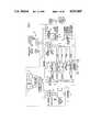
- FIG. 1is a block diagram of a computer system employing the present invention.
- FIG. 2is an illustration of the local bus structure of the system of FIG. 1.
- FIG. 3depicts the system bus node space assignments of the system of FIG. 1.
- FIG. 4A and FIG. 4Brepresent a block diagram of a memory controller contained in the memory system of the system of FIG. 1.
- FIG. 5is an illustration of the memory array bus structure of the memory system of FIG. 4.
- FIG. 6is a block diagram illustrating the configuration of the bus of FIG. 5.
- FIGS. 7, 7A and 7Bare timing diagrams showing the RETRY sequence.
- the systemincludes a single chip microprocessor 10, a floating point coprocessor 11, a memory controller 12, a local RAM 13, a local ROM 14, an off board memory 15, a time of year (TOY) clock 25, an Octal ART 26, a PAL 20, a system bus interface 16 and 24, latches 28 and transceivers 27, 32 and 34.
- the system components 10, 11, 12, 13, 14, 15, 16are interfaced with one another by means of a bus 17.
- the system components 10, 11, 12, 13, 14, 15, 16, 17are interfaced through the bus interface 16 to bus 18.
- a preferred system configuration for advantageous implementation of the teaching of the inventioncomprises a single board computer module 9 which contains system components 10, 11, 12, 13, 14, 16 24, 25, 26, 20, 24, 28, 27, 32, 34, 30, 31 AND BUS 17.
- the single board computermay be a module which is 32-bit, single-board processor that provides VAX functionality.
- the moduleis compatible with system bus 18 which is manufactured by Digital Equipment Corporation and hereinafter referred to as the system bus.
- VAXrefers to a product line manufactured by Digital Equipment Corporation.
- the module 9may function either as a primary or a secondary CPU in a larger computer configuration.
- the module 9thus serves as a computational engine for an operating system and for user application programs.
- the module 9implements console functions.
- a console 100provides the user interface to the module 9 and to the system configuration in which it is used. Through console 100, a user can bootstrap the system image, invoke diagnostic routines, examine or write registers and memory throughout the system bus 18 configuration, and interactively communicate with the operating system and application programs.
- the module 9provides an asynchronous serial interface 35 (RS-232C compatible) for up to eight terminals 103.
- the terminalsoperate independently of the console subsystem.
- the module 9has extensive on-board diagnostics. On power-up or node reset, it tests itself and makes its status (pass or fail) available over the system bus 18. A set of LEDs on the printed circuit board of module 9 also indicates the outcome of self-test. In addition, a user can invoke other on-board diagnostics to test the logic and functions of module 9 more extensively.
- the microprocessor chip 10 in the illustrated embodimentis a 32-bit, virtual-memory processor chip. Chip 10, for example, can directly address a 1 Gbyte physical address space.
- the floating-point unit 11(78132) is a single-chip, floating-point processor 11 that functions as a slave to the processor 10.
- the floating-point unit (FPU)performs 32-bit, floating-point computation and accelerates the execution of certain integer and character-string instructions.
- the local bus 17is a 32-bit, asynchronous, bidirectional bus that connects the processor 10 with on-board memory 13 and 14 and 14 and on-board devices.
- the local bus 17is time-multiplexed so that address information and data are transmitted over the same lines during different cycles of transaction.
- the local bus interface logic 19connects the local bus 17 with the processor 10, the chip 16, and components on the memory bus 22 (MBUS).
- the processor 10 and chip 16 transceiversgenerate byte parity on writes and check byte parity on reads.
- the bus transceiversare controlled by the MBUS PAL 20.
- the memory bus 22connects local memory, as well as other devices, to the local bus 17.
- the MBUS 22is a 32-bit data bus that interfaces with the local bus 17 through transceivers 27. With the exception of the real-time clock chip 25, the MBUS devices are addressed over a physical address (PA) bus 23. During the address part of a local bus cycle, local bus address bits [29:0] are latched by the PA latches 28.
- PAphysical address
- the module 9has 1 Mbyte of on-board RAM 13. Byte parity is generated for RAM writes, and it is checked on RAM reads.
- the RAMcan be backed up by batteries.
- the module 9has 128 Kbytes of ROM 14 that store firmware to perform initialization routines, the primary bootstrap routine, console program code, diagnostic routines and in-circuit tester pattern-generating code.
- the module 9can accommodate up to 256 Kbytes of ROM.
- the memory controller 12controls access to the physical address space.
- the memory controller 12decodes the address on the PA bus 23, enables the appropriate device, and returns status information to the local bus master.
- the memory controller 12also drives on-board RAM 13 and provides refresh timing for all local RAM, which includes off-board RAM on memory array modules 15.
- the primary processor in the systemwhich could be the module 9 itself, assigns the module 9 a starting address offset (SAO).
- SAOrepresents the base address for local RAM within system physical memory space.
- the memory controller 12uses the SAO to decode memory references. If the module 9 is not the primary processor, the console software assigns the starting address from the system Starting Address Register.
- the memory array bus 21is an off-board extension of the local bus 17.
- the memory array bus 21connects the module 9 with daisy chained memory array boards 15 in accordance with the present invention.
- the memory array bus 21thus allows the module 9 to access an extended main memory.
- Each memory array board 15contains 2 Mbytes of dynamic RAM implemented on 256 Kbyte memory chips. Up to five memory array boards 15 can be daisy chained to module 9 memory array bus 21. Main memory can thus be expanded to a total of 11 Mbytes (1 Mbyte on-board plus 10 Mbytes on memory array boards 15).
- the local bus masterrecognizes there is no distinction between the on-board RAM 13 and memory array board 15.
- the access time and other operating characteristicsare identical.
- Memory array board 15can also be backed up by batteries.
- the local bus 17 and the system bus 18interface through interface chips 16 and 24.
- Chip 24is a standard user interface to the system bus 18.
- the chip 16, which connects to the chip 24 through a bus 33,is a memory-mapped peripheral device of the processor 10.
- the chip 16is the window of module 9 onto the system bus 18.
- the chip 16translates the local bus 17 transaction into a transaction on the system bus 18.
- the chip 16translates the incoming system transaction into a local bus 17 transaction.
- the chip 24implements the system bus 18 commands and performs system error checking and arbitration.
- the console 100is the primary user interface to module 9 and to the system computer system as a whole.
- the consoleconsists of an RS-232C interface 30, a control panel 29, and console firmware that implements console commands.
- a DLART (DIGITAL Link asynchronous receiver/transmitter) chipprovides parallel-to-serial and serial-to-parallel conversion between the processor chip 10 and the RS-232C transceivers 30.
- the consolehas two operating modes: program mode and console mode.
- program modecharacters typed at the console terminal are passed to the operating system; this is the normal operating mode (run mode).
- console modecharacters typed at the console terminal are interpreted as console commands; the operating system and all application programs are suspended.
- the module 9provides an asynchronous serial interface 35 (RS-232C compatible) for up to eight terminals 103.
- This interfaceis implemented in an octal ART 26 (octal asynchronous receiver/transmitter) chip.
- the octal ART 26supplies eight independently programmed serial lines.
- One line (line 0)has modem-control signals that enable communication with a modem.
- the module 9provides a time-of-year (TOY) clock and a real-time clock. Both clock functions are implemented in the Motorola RTC chip 25 (MC146818). This chip 25 calculates and stores the time and date during system operation.
- the TOY clock 25has 50 bytes of battery-backed up RAM used by the console firmware to store the state of processor 10 when console mode is entered.
- the real-time functionpermits programmable interrupts to the processor chip 10.
- the local (integrated circuit interconnect) bus 17is a 32-bit, asynchronous, bidirectional bus.
- the local bus 17interfaces the processor chip 10 with local memory and on-board logic and supports direct memory access (DMA) transfers to and from local memory and the system bus.
- DMAdirect memory access
- the local bus 17is time-multiplexed. That is, address information and data are transmitted over the same lines during different parts of the bus cycle. Toward the beginning of the cycle, the address is transmitted. Toward the end of the cycle, data is transmitted.
- the bus masterinitiates and controls the transaction.
- the slaveresponds to the bus master's commands and returns appropriate status information.
- the local bus 17is an interlocked bus in that only one transaction can be on the bus at any given time.
- Data transfers on the local bus 17occur on naturally-aligned longword (32-bit) boundaries. For example, memory fetches occur on address boundaries ending in 0, 4, 8 and C (hex).
- the bus masterasserts the appropriate Byte Mask lines to indicate which bytes within a transferred longword contain valid data.
- the local bus's 17 data and control signalsare divided into classes.
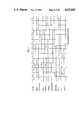
- FIG. 2depicts the local bus 17 structure and also delineates the classes of signals.
- the first classis information transfer signals and that encompasses 32 data and address lines and 4 lines for byte mask information.
- the second classis bus control and it entails control signals such as write, address strobe, data buffer enable, data strobe, ready and error.
- the third class of signalsis system control which is comprised of 3 lines of cycle status and reset.
- the fourth class of signalsis DMA (direct memory access) control which contains DMA request and DMA grant.
- the last class of signalsis interrupt control which is comprised of 4 lines for interrupt request, powerfail, halt and interval timer interrupt.
- the data and address linesare 32 bidirectional lines that are time-multiplexed.
- DAL [31:0]provide address and control information via DAL [31:30] to indicate the length of data to be transferred as follows:
- DAL [1:0]are the byte address but may differ from the address implied by BM [3:0] during an instruction prefetch (always an aligned longword), during a character string data prefetch (always an aligned longword), during a PTE (page table entry) read (always an aligned longword) or during the second cycle of an unaligned operation.
- DAL [31:0]transmit data from the bus master to the slave device.
- DAL [31:0]transmit data from the slave to the bus master.
- DAL [31:0]are also used for interrupt acknowledge cycles, external processor cycles and external processor register cycles.
- DAL [4:0]output the interrupt priority level (IPL) of the interrupt.
- IPLinterrupt priority level
- DAL [9:2]input the interrupt vector.
- the processor chip 10does not implement all the internal processor registers (IPRs) specified in the VAX architecture. These omitted IPRs are implemented externally and accessed through MTPR (Move to Processor Register) and MFPR (Move from Processor Register) commands. In the module 9 the console registers in the DLART chip are accessed as external processor registers. These bus cycles are similar to external processor cycles.
- IPRsinternal processor registers
- the Byte Mask signalsspecify which bytes on DAL [31:0] contain valid information during the data transfer part of a read or write cycle.
- DAL [31:24]contain valid data.
- BM [2]is asserted
- DAL [23:16]contain valid data.
- BM [1]is asserted
- DAL [15:8]contain valid data and when BM [0] is asserted, DAL [7:0] contain valid data.
- the Byte Mask signalsindicate which bytes the slave device must place on DAL [31:0].
- the bus masterignores bytes that do not contain valid data.
- the Byte Mask signalsindicate which bytes on DAL [31:0] contain valid data.
- the slave deviceignores the masked bytes.
- all four Byte Mask signalsare asserted.
- the Byte Mask signalsare valid only when the Address Strobe line (AS) is asserted.
- the Write linespecifies the direction of a data transfer on DAL [31:0]. If the bus master asserts WR, then it will drive data onto DAL [31:0]. If the bus master does not assert WR, then the slave device will drive data onto DAL [31:0]. WR is valid only when AS or EPS is asserted.
- the Address Strobe lineprovides timing information for address transfers.
- the bus masterasserts AS when the address on DAL [29:2] is valid during a read, write, or interrupt acknowledge cycle.
- the bus masterdeasserts AS at the end of the bus cycle.
- the Data Buffer Enable linein conjunction with WR, controls the DAL transceivers.
- the bus masterasserts DBE to enable the transceivers and deasserts DBE to disable them.
- the Data Strobe lineprovides timing information for data transfers.
- the bus masterasserts DS to indicate that it is ready to receive incoming data.
- the bus masterthen deasserts DS to indicate that it has received and latched the incoming data.
- the bus masterasserts DS to indicate that DAL [31:0] contain valid write data.
- the bus masterthen deasserts DS to indicate that it is about to remove the write data from DAL [31:0].
- External logicasserts the Ready line to indicate the normal termination of a read, write, or interrupt acknowledge cycle.
- thisindicates that the slave device will place the required data on DAL [31:0].
- thisindicates that the slave device has received data on DAL [31:0].
- an interrupt acknowledge cyclethis indicates that the interrupt vector has been placed on DAL [31:0].
- RDYWhen the bus master recognizes an asserted RDY, it terminates the current bus cycle. External logic then deasserts RDY.
- External logicasserts the Error line to indicate the abnormal termination of a read, write, or interrupt acknowledge cycle. After receiving an asserted ERR, the bus master terminates the current bus cycle. External logic then deasserts ERR. On receiving an asserted ERR, the processor chip executes a machine check.
- a response PAL 41 in the memory controller 12asserts ERR whenever a parity error occurs on a read from local RAM 13, provided that parity error reporting is enabled.
- Cycle Status signalsin conjunction with WR, provide status about the current bus cycle.
- ASis asserted during a read, write, or interrupt acknowledge cycle
- CS [2:0]are encoded as shown in Table 1.
- DMRDMA Request
- the processor chip 10asserts the DMA Grant (DMG) line to give external logic control of the local bus 17.
- the processor 10asserts DMG as long as external logic has control of the bus and deasserts DMG after external logic has deasserted DMR.
- the chip 16is the only device that requests and is granted control of the local bus 17. DMG is also asserted during retry cycles.
- the Interrupt Request signalsare the device interrupts to the processor chip 10. External logic asserts IRQ[3:0] to post interrupt requests.
- Each IRQ linehas a unique interrupt priority level (IPL).
- the processor 10accepts an interrupt request only if the request's IPL is higher than the IPL at which the processor 10 is currently operating.
- Each interrupt linealso corresponds to a unique IPL on the system bus. An incoming system interrupt is translated by the chip into a corresponding local bus device interrupt.
- IRQ [3:0]are level-sensitive signals that the processor chip 10 samples every cycle (200 ns).
- the processor 10synchronizes an IRQ signal internally.
- the processor 10accepts an interrupt request, it completes the current macroinstruction and then executes an interrupt acknowledge bus cycle. During this cycle, the processor 10 acknowledges the IPL at which the IRQ is posted and then inputs the vector for the interrupt.
- the chip 16inputs the acknowledged IPL and outputs the appropriate interrupt vector on DAL [9:2].
- the powerfail interrupt(BCI AC LO) is asserted to the processor 10. This interrupt vectors program control to a powerfail routine.
- the module 9asserts system DC LO L, indicating DC system voltages are about to fall below specification, the RESET line is asserted. RESET initializes the processor 10 and other logic on the local bus 17.
- HALTis a nonmaskable interrupt. HALT always interrupts the processor chip 10 after the current macroinstruction completes, regardless of the processor's 10 current IPL. HALT is an edge-triggered signal that is sampled every cycle (200 ns).
- interval counteroverflows every 10 milliseconds, thereby generating an interval timer interrupt (INTTIM) to the processor 10 at IPL 16.
- INTTIMinterval timer interrupt
- the interval counteris controlled by the Interval Clock Control Register (ICCR), an IPR in the processor 10.
- ICCRInterval Clock Control Register
- the counteris enabled when bit [6] in the ICCR is set and disabled when bit [6] is clear.
- the module 9supports different local bus 17 cycle types.
- the typesinclude idle, read, write, interrupt acknowledge, DMA and retry.
- DAL [31:0]are asserted but are undefined, and the bus control signals are deasserted.
- An idle cyclelasts four clock phases (nominally 200 ns).
- the bus masterinputs data from memory or an on-board I/O device.
- a CPU read cyclelasts at least eight clock phases (nominally 400 ns) and may last longer in increments of four clock phases (nominally 200 ns).
- the bus masterdrives a physical longword address onto DAL [29:2].
- the bus masterasserts BM [3:0] as required and deasserts WR.
- the bus masterasserts AS, indicating that the address is valid, and then asserts DS, indicating that DAL [31:0] are free to receive incoming data. If no error occurs, the slave device drives the required data onto DAL [31:0], and external logic asserts RDY. If an error occurs, external logic asserts ERR, which aborts the bus cycle. This causes the processor 10 to execute a machine check. Finally, the bus master deasserts AS and DS to end the cycle.
- a CPU write cycleIn a CPU write cycle, the bus master outputs data to memory or an on-board I/O device.
- a CPU write cyclelasts at least eight clock phases (nominally 400 ns) and may last longer in increments of four clock phases (nominally 200 ns).
- the bus masterdrives a physical longword address onto DAL [29:2].
- the bus masterasserts BM [3:0] as required and asserts WR.
- the bus masterasserts AS, indicating that the address is valid.
- the bus masterthen drives data onto DAL [31:0] and asserts DS, indicating that the data is valid on DAL [31:0]. If no error occurs, the slave device reads the data, and the external logic asserts RDY. If an error occurs, external logic asserts ERR, which aborts the bus cycle. This causes the processor 10 to execute a machine check. Finally, the bus master deasserts AS and DS to end the cycle.
- an interrupt acknowledge cyclethe processor chip 10 acknowledges a posted interrupt and inputs an interrupt vector.
- An interrupt acknowledge cyclelasts at least eight clock phases (nominally 400 ns) and may last longer in increments of four clock phases (nominally 200 ns). The detailed timing of an interrupt acknowledge cycle is identical to that of a CPU read cycle.
- the processor 10outputs on DAL [4:0] the IPL of the interrupt being acknowledged.
- the processor 10then asserts AS to indicate that DAL [4:0] contain a valid IPL.
- the chip 16reads the IPL from the bus.
- the processor 10then asserts DS to indicate that DAL [9:2] are free to receive the interrupt vector.
- the chipoutputs the appropriate interrupt vector on DAL [9:2]. If an error occurs, external logic asserts ERR, which causes the processor 10 to ignore the data and abort the transaction. Finally, the processor chip 10 deasserts AS and DS to end the interrupt acknowledge bus cycle.
- the processor 10initiates the cycle by driving the cycle status onto CS [1:0], precharging and sustaining CS [2] high, and asserting EPS.
- the external processorresponds by placing the required information on DAL [31:0].
- the processor 10reads the information on DAL [31:0] and deasserts EPS.
- the external processorthen removes the information from DAL [31:0] to end the cycle.
- the processor chip 10In an external processor write/command cycle, the processor chip 10 outputs either a command or data to an external processor.
- the cyclelasts four clock phases (nominally 200 ns).
- the processor chip 10relinquishes control of the local bus 17 to an on-board DMA device.
- the cyclebegins when a DMA device (the chip) asserts DMR to request control of the bus.
- the processor 10tri-states DAL [31:0], AS, DS, WR, and DBE; drives high and tristates BM [3:0] and CS [2:0], and asserts DMG.
- the DMA devicemay now use the bus to transfer data.
- the DMA devicestops driving AS, DBE, and DS and deasserts DMR.
- the processor 10then deasserts DMG and begins the next bus cycle.
- the processor chip 10If a transaction request is not granted, the processor chip 10 retries the transaction.
- the local bus 17 addressis stored in the chip.
- the local bus 17supplies eight hardware interrupts to the processor 10. Four of these interrupts are external and four are internal. External interrupts allow on-board devices to interrupt the processor 10. Internal interrupts alert the processor 10 to impending power failures, console halt requests, and interval timer overflows.
- the Interrupt Request lines, IRQ[3:0],are the four external interrupts. IRQ [3:0] are assigned IPLs 17 through 14 (hex), respectively. The higher the IPL, the higher the interrupt priority. The processor 10 responds to an interrupt request when the request's IPL is higher than the IPL at which the processor 10 is currently operating.
- the processor 10responds to an external interrupt after completing the current macroinstruction by executing an interrupt acknowledge bus cycle. During this cycle, the processor 10 outputs the IPL of the interrupt on DAL [4:0], and then inputs the interrupt vector from the requesting device on DAL [9:2]. In the module 9, the chip inputs the IPL and outputs the appropriate vector for all interrupt acknowledge cycles.
- the three external events which generate internal interrupts to the processor 10are (1) pressing the BREAK key on the console terminal keyboard (if the halt-on-BREAK function is enabled), (2) a power failure and (3) an interval counter overflow.
- Internal interruptsdo not cause the processor 10 to execute an interrupt acknowledge bus cycle. Instead, program control is vectored to a routine appropriate to the type of internal interrupt.
- the module 9 system control unit in the systemasserts system AC LO L, which generates a powerfail interrupt to the processor 10 at IPL 1E. This interrupt vectors the processor 10 to a powerfail routine.
- interval counteroverflows every 10 milliseconds, thereby generating an interval timer interrupt (INTTIM) to the processor 10 at IPL 16.
- INTTIMinterval timer interrupt
- Interval timer interruptsare controlled by the Interval Clock Control Register (ICCR), an IPR in the processor 10.
- ICCRInterval Clock Control Register
- Setting bit [6] in the ICCRenables the interrupts. Clearing this bit disables the interrupts.
- On-board peripheral devicesrequest and are granted control of the local bus 17 through DMA Request (DMR) and DMA Grant (DMG), respectively.
- DMRDMA Request
- DMGDMA Grant
- the chipuses DMAs to transfer data between the local memory 13 and the system bus 18.
- the Error line on the local bus 17alerts the bus master to an error condition during the current bus cycle.
- the memory controller 12asserts ERR whenever a parity error occurs on a read from local RAM 13, provided that parity is enabled. This causes the processor 10 to perform a machine check.
- the local bus 17carries a 28-bit physical address on DAL[29:2] that can reference 1 Gbyte physical address space.
- the local bus address spaceis equally divided into I/O space and memory space. For I/O references, address bit [29] is cleared. All on-board peripheral devices and ROM 14 reside in local bus 17 I/O space.
- Local RAM 13resides in local bus memory space.
- the module 9communicates with other system bus 18 nodes by interfacing the local bus 17 to the system bus 18. This interface lets the module 9 access I/O controllers, bus adapters, system memory modules, and other system processors.
- the chip 24connects directly to the system bus 18.
- the BCI buswhich is the standard user interface to the system bus 18.
- the chip 24appears to be the system bus.
- the BII chipalso implements the system protocol and error checking.
- the chip 16 chipinterfaces the local bus 17 to the BCI bus 33.
- the BCI bus 33is the user side of the chip 24 chip.
- the 16is thus the window on the system bus 18.
- the processor 10sees the chip 16 as a memory-mapped peripheral device.
- a response PAL 41(see FIG. 4) asserts system REFERENCE to the chip 16.
- the chip 16aided by the chip 24, then translates the local bus 17 transaction into a system transaction.
- the chip 16Whenever the module 9 processor issues a read or write to non-local I/O space, the chip 16 automatically translates the transaction onto the system bus 18. The chip 16 reports the status of windowed transactions back to the processor 10.
- the chip 16aided by the chip 24, translates incoming system transactions into local bus 17 transactions.
- the chip 16reports the transaction's completion status and, if appropriate, returns data to the originating system node.
- the chip 16If contention arises between an incoming system transaction and an outgoing local bus 17 transaction, the chip 16 asserts RETRY to a retry PAL 40 (see FIG. 4) in the memory controller 12. The retry PAL 40 then suspends the outgoing local bus 17 transaction until the incoming system transaction completes. The chip 16 stores the address for all local bus 17 transactions in its Retry Address Latch. When a suspended local bus 17 transaction is retried, the memory controller 12 fetches the stored local bus 17 address from the chip 16.
- the chip 16provides an interrupt controller for the processor chip 10. When the processor chip 10 acknowledges an interrupt from any source, the chip 16 inputs the acknowledged IPL (interrupt priority level) and supplies the processor 10 with the appropriate interrupt vector. In addition, the chip 16 translates system interrupts targeted at the module 9 processor into corresponding local bus 17 interrupts to the processor 10.
- IPLinterrupt priority level
- the chip 16provides 14 general purpose registers in the node space.
- GPR 1the Receive Console Data (RXCD) Register, is the console interface to the system bus 18.
- RXCDReceive Console Data
- GPR 5the Permanent Power-Up Diagnostic Register, stores a copy of the system self-test results.
- GPRs 7 through 11are used by the console entry sequence.
- GPR 11the Console Status Register, contains status on initialization. The rest of the chip 16 GPRs are not used.
- the chip 16implements two functions that the processor 10 does not use during normal operation but that may be useful for diagnostic purposes and special operations.
- the processor 10can construct commands for the system bus 18 by writing certain chip 16 registers.
- the chip 16also contains a special data mover that can move data over the system bus in octal word packets.
- the Console Display/Control Registerprovides direct reads of several control lines on the system bus 18.
- the CDCRcan also be written by the processor chip 10 to assert system RESET L and system BAD L on the system bus 18.
- the system node identification number of module 9is determined by four signal pins on the system backplane. This node ID number is independent of the slot location of module 9 in the system card cage. On power-up or reset, the node ID is loaded into the system Control and Status Register of the chip 24. The node ID determines which 8 Kbyte block in system nodespace is assigned to the module 9. This block contains the addresses of the system accessible registers. Blocks of nodespace are allocated according to the mapping scheme shown in FIG. 3.
- the system bus 18 registerswhich have addresses in system nodespace, are accessible to other system nodes. System access to the local RAM is determined by the Starting Address and Ending Address Registers in the chip 24. These registers are loaded on power-up or reset by the primary processor in the system (which could be the module 9 itself). During normal operation, all of the local RAM 13 is accessible over the system bus 18.
- Table 2describes the implementation of the system commands by module 9. Since the processor 10 does not have cache memory, it does not issue read or write commands with the intention of caching data.
- the memory controller 12When the reference is a nonlocal memory address, the memory controller 12 asserts system REFERENCE to the chip 16. The chip 16 then translates (windows) the local bus 17 transaction into a system transaction. Normally, the local bus 17 is unavailable for other transactions until the windowed system transaction completes. However, if the chip 16 receives an incoming system bus 18 transaction, it takes control of the local bus 17 to service the transaction and then restarts the interrupted local bus 17 transaction. If the system transaction completes successfully, the chip 16 asserts the Ready line. Otherwise, the chip 16 interrupts the processor 10 or, for serious errors, asserts the Error line.
- Table 3lists the translated local bus 17 transactions and their system counterparts.
- Table 4indicates the conditions on the system bus 18 that cause the chip 16 to assert the Error line to the processor 10.
- the chip 16When the module 9 (processor 10) is addressed over the system bus 18, the chip 16 asserts the DMA Request line (DMR) to the processor 10 to request mastership of the local bus 17. When granted bus mastership, the chip 16 translates the incoming system transaction into a local bus 17 transaction. The system bus 18 is interlocked during translated local bus 17 reads but not during translated local bus 17 writes. When the local bus 17 transaction completes, the chip 16 reports the completion status and, if appropriate, transfers data to the originating system node;
- DMRDMA Request line
- Table 5lists the system transactions to which the module 9 responds and their local bus 17 translations.
- Table 7indicates how the chip 16 translates local bus 17 status onto the system bus 18. Quadword and octaword transactions on the system bus 18 are translated into a series of longword transaction on the local bus 17.
- the module 9 moduleaccepts both Interrupt (INTR) commands and Interprocessor Interrupt (IPINTR) commands from the system bus 18.
- INTRInterrupt
- IPINTRInterprocessor Interrupt
- the chip 16On receiving an INTR command, the chip 16 asserts the corresponding local bus 17 Interrupt Request (IRQ) line.
- System IPLs BR 7-4correspond to local bus 17 interrupts IRQ [3:0], respectively.
- the processor chip 10responds to the interrupt request by executing an interrupt acknowledge transaction, which the chip 16 windows onto the system bus 18 as an IDENT transaction.
- the chip 16inputs the vector from the interrupting node and returns this vector to the processor chip 10.
- the chip 16On receiving an IPINTR, the chip 16 asserts IRQ [14] to the processor chip 10. When the processor chip 10 acknowledges the interrupt request, the chip 16 returns 80 (hex), the vector for all IPINTRs.
- the module 9supports both local memory 13 (on-board dynamic RAM), expansion memory (off-board RAM) on memory array boards 15, which are daisy chained, and 128 Kbytes or 256 Kbytes of on-board ROM 14.
- the module 9does not have cache memory.
- the module 9has one Mbyte of on-board RAM 13, which is composed of 256 Kbyte dynamic RAM chips.
- the local bus 17 master(processor 10 or chip 16) can access this memory only on naturally-aligned longword boundaries. However, the bus master can use the Byte Mask signals to specify which bytes in a transferred longword contain valid data.
- On-board RAM 13is parity protected. Byte parity is written to RAM on all writes and checked on all reads. Parity generation and checking is performed by the processor transceivers (for processor-initiated transactions) and by the chip 16 transceivers (for chip 16-initiated transactions). Parity is generated and checked only for bytes specified to be valid by the Byte Mask signals.
- the memory access timedepends on the local bus 17 master.
- a processor 10 initiated read cycletakes 400 ns, while a chip 16 initiated read cycle takes 50 to 100 ns longer, due to the synchronization requirements of chip 16. Write cycles are the same for both bus masters.
- the system of the present inventioncan support a plurality of memory array boards 15 daisy chained to the memory array bus 21, as will appear.
- each memory array board 15contains two Mbytes of RAM.
- Each boardis driven by its own on-board logic and by bus control signals.
- Off-board RAMsupports byte parity, masked reads and writes, and has the same access times as does on-board RAM.
- memory array boards 15must be placed in slots adjacent to the board 9. There can be no intervening slots or boards between the memory array boards 15 and the board 9.
- the main memory and the memory controller 12support longword read, read interlock, longword write, masked longword write and unlock write mask memory cycle types. All memory bus cycles are on naturally-aligned longword boundaries.
- a longword readis a simple read from memory.
- the read interlock bus cyclelocks all of main memory so that another read interlock cannot access memory until the lock is cleared. However, noninterlocked types of read operations can still access memory.
- a read interlocksets the Memory Locked bit in the memory controller 12.
- a longword writeis a simple write to memory. In the masked longword write, certain bytes within the referenced longword may be masked out.
- the Byte Mask signalsindicate which bytes are valid.
- the unlock write maskclears the lock on main memory set by a previous interlock read. An unlock write mask clears the Memory Locked bit in the memory controller 12.
- the initialization codeon power-up or node reset, the initialization code sizes the local RAM 13 and makes the size available in chip 24 GPR 1.
- the module 9then assigns a starting address offset (SAO) to the local RAM 13.
- SAOstarting address offset
- the SAOis the base address of the local RAM 13 in system memory space. If the module 9 is a secondary processor, the SAO value is based upon the contents found in the chip 24 Starting Address Register (SADR).
- the module 9contains independent power connections for battery-backup voltages. When provided, battery backup maintains the local RAM 13 and refresh circuitry. Battery-backup voltage is monitored by the system control unit.
- the standard 128 Kbyte ROMprovides 32K longword locations at addresses 2004 0000 hex through 2004 5FFF hex.
- the optional 256 Kbyte ROMprovides 64K longword locations at addresses 2004 0000 hex, through 2004 7FFF hex. Both ROM configurations are accessed on naturally-aligned longword boundaries.
- the 128 Kbyte ROM 14 configurationhas a 15-bit address (PA [16:2]).
- the 256 Kbyte ROM configurationuses the same 15 address bits plus the signal 256 Kbyte ROM as the 16th (high-order) address bit.
- the signal 256 Kbyte ROMis allowed to float, that is, the bit is not connected to the ROM chips and therefore can be neither high nor low.
- the signal 256 Kbyte ROMmust be connected to the ROM chips by adding a jumper to the module. The jumper connects ROM address 17 coming from the processor physical address latch with the 256 Kbyte ROM signal.
- the standard 128 Kbyte ROM 14provides 32K longword locations, but the total ROM space can accommodate 64K longwords. To completely fill the available boot ROM space, the 32K body of ROM code is replicated twice throughout this range of addresses.
- Corresponding addresses from each setmap to the same longword. This complete coverage of ROM space eliminates errors resulting from referencing nonexistent (unimplemented) locations. If a nonexistent location is referenced, the data returned is undefined.
- the standard ROM configuration 14contains the initialization routines, the primary bootstrap routine (VMB), diagnostic routines, and the console program, which are written in macrocode.
- program controljumps to the first location, 2004 0000 hex, in boot ROM space, and the module 9 executes its initialization routine. Note that the initialization code resides in the I/O space at addresses 2004 0000 hex, through 2008 0000 hex.
- the primary bootstrap's main functionis to locate the secondary bootstrap routine, bring it into memory, and then transfer control to it. The secondary bootstrap then loads the operating system.
- the primary bootstrapalso performs the following initialization in which it, tests all of local memory and builds a bit map that flags physical memory pages (512 Kbytes each) as good or bad, finds out what devices are present and operative in the system, and sets up the restart parameter block (RPB), a data structure used by powerfail and recovery routines to save volatile processor state.
- RPBrestart parameter block
- VMBcontains a boot driver that loads the secondary bootstrap program into memory and also writes a dump file to disk if the operating system detects a fatal error.
- the diagnostic codeconsists of a self-test, which runs automatically on power-up and reset, and additional diagnostics, which can be invoked from a console.
- the self-testprovides a quick confidence check of the hardware at the node, including any attached memory array boards 15.
- the additional diagnosticstest the module 9 more extensively.
- the diagnostic codealso contains a parser that parses diagnostic commands.
- the memory controller 12controls access to the on-board memory, registers, and devices, as well as access to off-board memory that resides on attached memory array boards 15. Whenever the processor 10 or chip 16 references the physical address space, the memory controller 12 decodes the physical address and the local bus 17 cycle type, and provides completion status to the local bus 17 master. In addition the memory controller 12 controls the addressing of on-board RAM 13, refresh timing for both on-board and off-board RAM 15, parity error reporting and local bus retry timing.
- FIG. 4is a block diagram showing the major components of the memory controller 12. These include I/O address PAL 45, memory address comparator 44, status PAL 43, cycle PAL 42, response PAL 41, retry PAL 40, DRAM controller chip 46, parity error logic and the memory control and status registers (MCSRs) 47.
- I/O address PAL 45memory address comparator 44
- status PAL 43cycle PAL 42
- response PAL 41response PAL 41
- retry PAL 40DRAM controller chip 46
- MCSRsmemory control and status registers
- the I/O address PAL 45decodes all addresses on the physical address (PA) bus 23.
- the addresscan be a memory address or an I/O address.
- the I/O address PAL 45asserts KASPC (module 9 SPACE) to the response PAL 41, indicating that the address is implemented.
- the PAL 45also selects or enables the referenced device which includes ROM 14, CDCR (Console Display/Control Register) PAL, Octal ART chip 26, MCSRs 47 (Memory Control and Status Registers) and TOY (time-of-year) clock 25.
- the I/O referenceis to an unimplemented I/O location (addresses 2008 5000 hex through 203F FFF hex)
- the address PAL 45asserts NSSPC (Nonsupported Space) to the response PAL 41.
- the response PAL 41then asserts RDY to the local bus 17 master, however, the data on DAL [31:0] is undefined.
- the memory address comparator 44decodes all addresses on the physical address (PA) bus 23.
- the comparator 44inputs PA [29:28] and compares address bits DAL [27:0] with the starting address offset (SAO [7:0]) for local RAM 13.
- the starting address offsetspecifies the local RAM's 13 base address in system memory space.
- PA [29]is set, the reference is to I/O space, otherwise, the reference is to memory space. If PA [28] is set, the reference is above the upper limit, 0FFF FFFF hex, of the 256 Mbyte address range supported by the memory controller 12, and therefore cannot be implemented in the local RAM 13. If both PA [29] and PA [28] are clear, the comparator compares DAL [27:0] with SAO [7:0]. If DAL [27:0] is less than SAO [7:0], the referenced address is below the starting address offset, and therefore cannot be implemented in local RAM 13. If DAL [27:0] matches SAO [7:0], the referenced address is to on-board RAM 13. If DAL [27:0] is greater than SAO [7:0], the reference is not to on-board RAM 13 but may be to off-board RAM 15, that is, RAM on memory array boards 15.
- the comparatoroutputs two signals, CPU NXM (CPU Nonexistent Memory) and LOW NXM (Low Nonexistent Memory) to the cycle 42 and response 41 PALs.
- CPU NXMCPU Nonexistent Memory
- LOW NXMLow Nonexistent Memory
- the memory referenceis to on-board RAM 13.
- the cycle PAL 42asserts RASIN (Row Address Strobe In) to the DRAM controller 46.
- the DRAM controller 46latches the PA address and outputs the address and control strobes for on-board RAM 13.
- CPU NXMis asserted
- the memory referenceis not to on-board RAM 13, but may be to off-board RAM 15 (RAM on the memory array bus 21). In this case, the attached memory array boards 15 take over the address decoding.
- the selected boardwill respond to the bus cycle. Otherwise, the BUS NXM (Bus Nonexistent Memory) is asserted to the response PAL 41, causing the PAL 41 to assert system REFERENCE to the chip 16.
- BUS NXMBus Nonexistent Memory
- the chip 16translates the transaction into a system transaction. If the bus cycle was initiated by the processor chip 10, the chip 16 translates the transaction into a system transaction. If the bus cycle is an incoming system transaction, the chip 16 returns NO ACK on the system bus 18. When LOW NXM is asserted, the memory reference is not to local RAM 13. This causes the response PAL 41 to assert system REFERENCE to the chip 16. If the bus cycle was initiated by the processor chip 10, the chip 16 translates the transaction into a system transaction. If the bus cycle is an incoming system transaction, the response PAL 41 asserts ERR on the local bus 17 and the chip 16 returns NO ACK on the system bus.
- the memory controller 12provides status information to the local bus 17 master (processor 10 or chip 16) during a memory cycle.
- the bus masteruses this status to control the cycle.
- the response logic for memory cyclesis implemented in the status PAL 43 and the response PAL 41.
- the status PAL 43has an internal flip-flop called the Memory Locked bit. This flip-flop sets when an interlock read bus cycle locks the local memory 13. If another interlock read is attempted while the Memory Locked bit is set, the status PAL 43 asserts RETRY. The unlock write mask bus cycle clears the Memory Locked bit. Normally, the interlock read and unlock write mask bus cycles are a paired transaction and are generated by the same bus master.
- the status PAL 43also reports parity errors by asserting ERROR PENDING to the response PAL 41. If parity checking is enabled, the response PAL 41 then asserts ERR to the bus master to indicate abnormal termination of the bus cycle. ERROR PENDING remains asserted until cleared by a subsequent D-stream (data stream) read or write cycle.
- the response PAL 41asserts RDY to the bus master. If the processor chip 10 is the bus master, the response PAL 41 asserts RDY during the first response window in the cycle. This allows the processor 10 to execute a 400-ns (nominal) cycle. If the chip 16 is the bus master, the response PAL 41 asserts RDY when read data is valid on the local bus 17, which results in a long bus cycle of 500 ns (nominal). The chip 16 receives RDY early in the cycle for writes, which allows a minimum length bus cycle.
- Table 7describes the sequence of responses of memory controller 12 to any given event in a memory cycle.
- Table 8describes the response.
- a DP8409 DRAM controller 46drives the on-board RAM 13.
- the DRAM controller 46generates the address, row and column address strobes, and refresh count for the 256 Kbyte DRAM chips.
- the Column Address Strobe (CAS) from the DRAM controller 46is divided into four CAS signals that are gated by BM [3:0]. When a Byte Mask line is asserted, the corresponding byte in the longword is to be read or written.
- CASColumn Address Strobe
- Memory access and refresh cyclesare controlled externally to the DRAM controller 46.
- the control logicis implemented in the cycle PAL 42 and the status PAL 43.
- the status PAL 43uses the synchronized Address Strobe (AS) and Refresh signals to arbitrate between memory and refresh cycles. When there is contention (both signals assert on the same clock edge), the memory cycle wins. If Synchronized Refresh alone is asserted, the PAL asserts the Refresh line to initiate a refresh cycle.
- ASAddress Strobe
- the status PAL 43allows memory refreshing while a windowed local bus 17 transaction is outstanding on the system bus 18. While waiting for the transaction to complete, the processor 10 asserts AS to interlock the local bus 17. Normally, this would prevent a refresh cycle from occurring. However, the status PAL 43 can detect this situation, and will allow refreshing even though AS is asserted.
- the cycle PAL 42controls the address timing for both on-board 13 and off-board RAM 15.
- the PAL 42asserts RASIN (Row Address Strobe In) and CASIN (Column Address Strobe In) to the DRAM controller.
- the DRAM controller 46synchronizes these signals internally and outputs RAS (Row Address Strobe) and CAS (Column Address Strobe) to the RAM.
- the cycle PAL 42asserts ARR RASIN (Array Row Address Strobe In) on the array bus.
- ARR RASINserves as the start pulse for off-board memory and refresh cycles.
- the retry PAL 40suspends and then restarts (retries) local bus 17 transactions initiated by the processor 10.
- the retry PAL 40suspends and then restarts (retries) local bus 17 transactions initiated by the processor 10.
- Byte parity on the local bus 17is generated for processor initiated transactions, by the processor transceivers 36, and for chip 16 initiated transactions, by the chip 16 transceivers. Parity is checked by the chip 16 transceivers 34.
- the memory controller 12When the parity error signal is generated, the memory controller 12 generates two parity error reporting signals called PERR and PARITY ERROR.
- PERRWhenever a parity error is detected, PERR is asserted. This sets the Parity Error bit in the Memory Status Register 47 (MCSR0) when the cycle PAL 42 asserts DONE to indicate that the bus cycle has finished.
- MCSR0Memory Status Register 47
- the Parity Error bitis only a status bit. It does not cause the operating system to respond to the parity error.
- PARITY ERRORis a logical AND of PERR and of the Parity Enable signal from the Memory Control Register 47 (MCSR1). If the Parity Enable signal is asserted, PARITY ERROR is asserted whenever PERR is asserted to the status PAL 43. The status PAL 43 then asserts Error Pending to the response PAL 44. The response PAL 41 terminates the bus cycle by asserting ERR to the bus master.
- the memory controller 12has four control and status registers.
- the memory status registerreports parity errors and enables latching of the address at which a parity error occurs.
- the memory control registercontrols parity reporting and indicates whether local memory was successfully sustained by battery backup when main system power was off.
- the memory configuration registerindicates the highest Mbyte boundary of the last memory array board 15 that was accessed.
- the memory starting address offset/error address register on power-up or resetis written to by the primary processor's memory configuration routine. The routine writes the starting address offset for local memory into this register. Under certain conditions, the register indicates the address of a memory location that was read with bad parity.
- additional memorymay be connected to the memory array bus.
- additional memoryis not required but instead there is a need of an I/O bus, e.g. when a connection to an external processor 400 must be made.
- I/Ocan be accommodated using the memory array bus, thereby eliminating the need for an additional I/O bus. In a single board processor this reduction in hardware is of great significance.
- the configuration bus 407is used for dual purposes. When used with memory, it provides unidirectional configuration information as described above. However, when used as an I/O bus, e.g., with an external processor 400, the bus becomes partially a bi-directional bus. The first four lines of the bus are taken off and provided into a bi-directional buffer 401. Inputs to this buffer are the signals CS0 and CS1 from the local bus 17. Outputs, which are obtained from the external processor 400 and provided into the buffer 401, are signals designated as STALL and RETRY. -The RETRY signal is the same signal described above and provides an additional input into the RETRY PAL 40.
- the seventh bit of the configuration busis utilized to indicate whether or not memory or an external processor is present on the end of the bus. If a memory is present, this bit is not asserted. If a processor is present the bit is asserted and this signal is provided as an input to buffer 401 to turn on the buffer and automatically convert what was a configuration bus into a bi-directional bus which permits operation as an I/O bus with an external processor.
- FIG. 6is helpful in further understanding this type of operation.
- system 412which includes the previously described processor 415, one megabyte of memory 421, interface 417 to interface with an external bus 419, status PAL 425 which controls the lock and retry logic and the retry PAL 423 itself. It of course includes all of the other hardware described above in connection with FIG. 4. Only this much of the apparatus is set out in block diagram form in order to give a better understanding of the reconfigured bus.
- a system 413including one or more processors 431 with, for example, 16 megabytes of dynamic random access memory 433 and lock and retry logic 435. Shown with the figure is a definition of what the configuration bus bits mean when configured with an external processor present.
- bit 1is a RETRY signal and bit 0 is a STALL signal.
- Bits 2 and 3are outputs from system 412 to system 413. The remaining bits 0, 1, and 7 are inputs from the system 413 to the system 412.
- the computer system 413can be a graphics system-of the type described in copending application Ser. No. 085,081, entitled High Performance Graphics Workstation, filed Aug. 13, 1987 and assigned to the same assignee as the present invention, the disclosure of which is hereby incorporated by reference.
- STALL and RETRYFor a better understanding of the general use of STALL and RETRY, reference may be made to the aforementioned copending application Ser. No. 534,720.
- RETRYcan be asserted within the system 412 under a number of conditions. First of all RETRY may be asserted, the lock bit is set. The lock bit is set if the processor 415 is to be denied access to the memory 421. Such can be initiated by the memory itself or may be caused because the bus 419 is accessing the memory. RETRY can also be asserted by the interface device 16 if it has an incoming transaction at the same time there is a request for an outgoing transaction from processor 10. As previously explained, what occurs during RETRY is that the cycle then present and being carried out by the processor 415 is aborted and subsequently restarted. In addition, the arrangement of the present invention permits also asserting RETRY remotely from the system 413.
- the processor 415at times requires access to the memory 433 in the system 413.
- the memory 433will be storing data structures. Data structures are quite large and for proper operation it is necessary that a complete data structure be obtained all at one time from memory.
- the processor 431is accessing memory 433 to obtain a data structure it can interlock its memory 433 by setting a lock bit in the logic 435. If the processor 415 now attempts to access the memory 433, the presence of this lock bit causes a RETRY signal to be sent back over the configuration bus 407 to the system 412 where it will become an input to the RETRY PAL and cause aborting and restarting of the cycle of processor 415 in a manner more fully described below.
- RETRYmay also be asserted as a result of the bus timeout specification of system 413, e.g. in order to refresh memory 433.
- Processor 415can also lock out the remote memory through the use of the two CS0 and CS1 bits which are also provided on the configuration bus, e.g. when it is accessing the memory to obtain a data structure.
- the STALL signalwhich is on bit 0 of the configuration bus in effect converts what is a synchronous bus when operated in the memory mode to an asynchronous bus when operated in the I/O mode.
- a normal memory cycle of the processor 413operates in a synchronous manner.
- the processorexpects to receive either a ready (RDY) or error (ERR) signal from response PAL 41 at a certain point in the cycle. Because of the fact that when operating with the system 413, it is operating with a system to which it is not synchronized, the bus cycle cannot always be completed at the proper time. What is done to avoid completion of the cycle is to assert the STALL signal on reconfigured bit 0. This may be done selectively or, as in the illustrated embodiment, each time the remote system is addressed.
- STALLis an input to the response PAL 41 of FIG. 4 and causes the response PAL 41 to delay providing the ERR or RDY output until STALL is no longer asserted.
- the processorin response to the STALL signal the processor extends its cycle. When STALL is asserted the cycle is suspended. Once the STALL signal is deasserted, the cycle continues and the response PAL 41 can provide the RDY signal or ERR signal.
- the need for some mechanism to resolve potential conflicts between the processor 10 and the requests on bus 18, as well cases where a memory, be it memory 13 or remote memory in a remote computer system 400,is clear in light of the foregoing overview of the system.
- the Retry method and apparatuswhich will now be described in detail provides that mechanism. It does so by operating various transceivers to electronically decouple processor 10 from the local bus 17, while at the same time storing the memory address which the processor 10 was using. During the time the processor 10 is decoupled, the potential conflict or deadlock is resolved by allowing the devices other than the processor 10 to perform their task. Upon resolution, Retry allows the processor 10 to resume operation by recoupling it to the local bus 17 and reasserting, from PAL 40, the proper addresses and signals. The method avoids the necessity of reinitializing processor 10 after such a break, which is required by some other systems, and also maximizes processor utilization.
- three eventscan trigger the occurrence of a Retry.
- the first of these eventsis when an outgoing local bus 17 transaction contends with a system bus 18 transaction. Since bus interface chip 16 cannot translate transactions in both directions at once, the outgoing local bus transaction is suspended and then retried after the incoming system bus 18 transaction has been completed.
- TOY clock 25has both a slow setup time and a slow access time.
- the Retry sequenceis thus well-suited for accessing this device.
- the final event which may trigger the Retry sequenceis when the processor 10 attempts an interlock read operation on memory, be it local memory 13 or memory in a remote processor coupled as described in connection with FIG. 6, when that memory is locked.
- Retrycould be implemented with a plurality of other input/output devices or with other computer architectures.
- the Retry sequencecommences when bus interface chip 16, the status PAL or the remote computer asserts RETRY or when the I/O address PAL asserts TOY.
- RETRY 500when RETRY 500 is asserted, due to LOCK 402 being low, retry PAL 40 deasserts the following control signals: (1) AS EN (address Strobe Enable) 404, (2) DBE EN 406 (Data Buffer Enable) and (3) BMEN (Byte Mask Enable) 408.
- AS ENaddress Strobe Enable
- DBE EN 406Data Buffer Enable
- BMENBinaryte Mask Enable
- the bus interface chip 16stores the address output of processor 10 in its Retry address latch.
- Retry Pending 419An internal flip-flop in retry PAL 40, called Retry Pending 419, is asserted (see FIG. 7A) to latch the address stored in bus interface chip 16 and to indicate to the retry PAL 40 that it must later restart the suspended local bus transaction.
- a retry pending input to Response PAL 41prevents it from asserting RDY or ERR.
- bus interface chip 16If the retry sequence was triggered in response to a signal from bus interface chip 16, in response to control signals asserted by processor 10, prior to asserting RETRY 500, bus interface chip 16 asserts DMR 420 (DMA Request), shown in FIG. 7A, to request that control of local bus 17 be given to the bus interface chip 16, as opposed to processor 10.
- DMR 420DMA Request
- processor 10would assert UV DMG (processor DMA Grant) to the retry PAL 40 causing the retry PAL 40 to assert DMG (DMA Grant) to bus interface chip 16.
- processor 10is waiting for acknowledgment from the stalled local bus 17 transaction and cannot assert UV DMG.
- Retry PAL 40senses that a retry is in progress, and takes over this function, and asserts DMG 422 to give the bus interface chip 16 bus control.
- the bus interface chip 16deasserts RETRY and takes control of the local bus 17 issuing control signals 424 and completes the incoming system bus 18 transaction. Then, the bus interface chip 16 gives up control of the local bus 17 by deasserting DMR at 430, which causes the retry PAL 40 to deassert DMG at 432.
- Retry PAL 40then restarts the stalled local bus 17 transaction with control signals at 434.
- retry PAL 40deasserts the DAL transaction control signals and asserts a TOY select. Retry PAL 40 then restarts the stalled local bus 17 transaction.
- the response PAL 41also restarts the transaction when the lock bit is cleared and DMG is deasserted. This is shown in FIG. 7B.
- the interface 16for example, asserts DMG at 450 and the processor asserts DMG at 451.
- the interface 16asserts the control signals starting the bus (read) cycle, indicating that it is a read lock.
- the lock bitis set in status PAL 43 by CS (1:0) at 455.
- processor 10asserts control signals and tries to read from memory at 457
- Retry 500is asserted by status PAL 43 causing Retry AL 40 to deassert the control signals at 458 and set the retry pending bit at 459.
- interface 16does a write unlock, which completes at 461
- the lock bitis cleared at 463
- Retry PAL 40 at 465asserts the control signals that were deasserted at 458.
- the local bus 17 transactionis restarted by the retry PAL 40 asserting Byte Mask Enable 408, which enables the processor 10 Byte Mask and Control Status lines.
- the retry PAL 40then asserts RLOE (Retry latch Output Enable) to output the stored address from bus interface chip 16.
- RLOE Delay 412a timing signal internal to retry PAL 40 is asserted, causing the Address Strobe Enable 404, and Data Buffer Enable 406 to assert at staggered intervals as shown in FIG. 7.
- These enable signalsgate processor 10 control signals to the local bus 17 at the proper intervals.
- the Retry sequenceis completed when the response PAL 41 asserts either RDY or ERR to the processor 10 chip to indicate a successful or unsuccessful completion of the transaction.
- processor 10By electronically isolating processor 10 from the local bus 17 during the previously described events, potential conflicts with other devices on the bus are avoided. Since the processor 10 is only suspended and the Retry PAL regenerates the beginning of the cycle, operation can resume without reinitializing the chip and with only a minimal loss of available processing capacity.
Landscapes
- Engineering & Computer Science (AREA)
- Theoretical Computer Science (AREA)
- Computer Hardware Design (AREA)
- General Engineering & Computer Science (AREA)
- Physics & Mathematics (AREA)
- General Physics & Mathematics (AREA)
- Software Systems (AREA)
- Multi Processors (AREA)
Abstract
Description
______________________________________ [31] [30] Length of Data ______________________________________ 0 0 Byte (8 bits) 0 1 Word (16 bits) 1 0 Longword (32 bits) 1 1 Quadword (64 bits) ______________________________________
__________________________________________________________________________T: PAL16R8 P: 23-175-K5-00 N: DENNIS HAYES RETRY D: 19-MAR-1987 S: CLK RETRY IIDMR -UVDMG -ST5 RESET -TOY -UVAS -MEMLOCK GND GND -TOY.sub.-- CYC -IIDMG -RET.sub.-- PEND -RLOE.sub.-- DEL DBE.sub.-- EN -AS.sub.-- EN -RLOE -BM.sub.-- EN VCC B: /-IIDMG= /-UVDMG *IIDMR *-RET.sub.-- PEND *-TOY.sub.-- CYC ;pass uVax dmg if dmr is asserted + IIDMR *-BM.sub.-- EN */-RET.sub.-- PEND ;generate dmg during retry + /-IIDMG *IIDMR */-RET.sub.-- PEND ;hold dmg during retry /-RET.sub.-- PEND= RETRY *-IIDMG *-RESET *-TOY.sub.-- CYC */-UVAS */-ST5 ;set ret.sub.-- pend when st5 sets + /-RET.sub.-- PEND *-DBE.sub.-- EN ;hold ret.sub.-- pend until dbe.sub.-- en sets + /-RET.sub.-- PEND *RETRY ;hold ret.sub.-- pend until retry clears + /-UVAS */-IIDMG /-BM.sub.-- EN= /-RET.sub.-- PEND */RETRY *-IIDMG *-MEMLOCK ; issue bm.sub.-- en after retry deasserts IIDMG *-RET.sub.-- PEND ; normal set path + /-BM.sub.-- EN *-RET.sub.-- PEND *-TOY.sub.-- CYC *-IIDMG ; normal hold path + /-RESET /-RLOE= /-RET.sub.-- PEND */RETRY *-IIDMG *-AS.sub.-- EN *-MEMLOCK + /-RLOE */-RET.sub.-- PEND */RETRY *-TOY.sub.-- CYC *-IIDMG *-AS.sub.-- EN + /-TOY.sub.-- CYC */RETRY *-IIDMG *-AS.sub.-- EN *-DBE.sub.-- EN + /-RLOE */-TOY.sub.-- CYC */RETRY *-IIDMG *-AS.sub.-- EN *-DBE.sub.-- EN /-RLOE.sub.-- DEL= /-RLOE */RETRY + /-UVAS */-TOY *-TOY.sub.-- CYC */RETRY *-RET.sub.-- PEND */-ST5 *-RESET + /-RLOE.sub.-- DEL *-TOY.sub.-- CYC *-RET.sub.-- PEND */-UVAS *-RLOE *-RESET /-AS.sub.-- EN= /-RLOE.sub.-- DEL */-RET.sub.-- PEND */-RLOE *-IIDMG ; retry sequence set + /-AS.sub.-- EN */RETRY */-RET.sub.-- PEND *-TOY.sub.-- CYC *-IIDMG ; retry hold path IIDMG *-TOY.sub.-- CYC *-RET.sub.-- PEND *-RLOE.sub.-- DEL ; normal set path + /-RESET ; reset set path + /-TOY.sub.-- CYC */-RLOE.sub.-- DEL */-RLOE *-IIDMG ; toy cycle set + /-TOY.sub.-- CYC */-AS.sub.-- EN *-IIDMG */-DBE.sub.-- EN ; toy cycle hold + /-RET.sub.-- PEND */-DBE.sub.-- EN /-DBE.sub.-- EN= /-AS.sub.-- EN */RETRY *-TOY *-TOY.sub.-- CYC *-IIDMG ;set path no activity or retry in progress + /-DBE.sub.-- EN *-RET.sub.-- PEND *-TOY *-TOY.sub.-- CYC *-IIDMG ;latch until event IIDMG *-TOY *-TOY.sub.-- CYC *-RET.sub.-- PEND ;deassert dbe.sub.-- en before as.sub.-- en + /-RESET ;reset set path + /-TOY.sub.-- CYC */-AS.sub.-- EN */-RLOE *-IIDMG */-RLOE.sub.-- DEL ;assert after address is on bus + /-TOY.sub.-- CYC */-DBE.sub.-- EN */-AS.sub.-- EN *-RLOE *-IIDMG ;hold until toy.sub.-- cyc is over /-TOY.sub.-- CYC= /-TOY *-RESET */-UVAS *-IIDMG *-AS.sub.-- EN + /-TOY.sub.-- CYC */-UVAS *-IIDMG E: END OF EQUATIONS __________________________________________________________________________
TABLE 1 ______________________________________ CS[1:0]WR 1 0 Bus Cycle Type ______________________________________ H L L RESERVED H L H Read data H H L RESERVED H H H Response enable L L L Write command (FPU) L L H Write data L H L Write command (non-FPU) L H H RESERVED ______________________________________
TABLE 2 ______________________________________ Issues Responds To ______________________________________ Single-Responder Commands READ Yes Yes RCI (Read with Cache Intent) No Yes IRCI (Interlock Read with Cache Intent) Yes Yes WRITE Yes Yes WCI (Write with Cache Intent) No Yes WMCI (Write Mask with Cache Intent) Yes Yes UWMCI (Unlock Write Mask with Yes Yes Cache Intent) IDENT (Identify) Yes Yes MULTI-RESPONDER COMMANDS INTR (Interrupt) Yes Yes IPINTR (Interprocessor Interrupt) Yes Yes BDCST (Broadcast) No Yes STOP Yes No INVAL (Invalidate) Yes No ______________________________________
TABLE 3 ______________________________________ Local bus Transaction System bus Transaction ______________________________________ Read READ Write WRITE Read Lock IRCI (Interlock Read with Cache Intent) Write Unlock UWMCI (Unlock Write Mask with Cache Intent) Interrupt Acknowledge IDENT (Identify) ______________________________________ *Longword transactions.
TABLE 4 ______________________________________ Read Transactions ______________________________________ A System bus retry timeout occurs. A stall timeout occurs. NO ACK is returned from the slave node. A System bus error occurs (for example, bad parity is detected on the System bus or an illegal confirmation code is returned). A Read Data Substitute code or Reserved read status code is returned from the slave node. ______________________________________ Write Transactions ______________________________________ A System bus retry timeout occurs. A stall timeout occurs. NO ACK is returned from the slave node. A System bus error occurs (for example, bad parity is detected on the System bus or an illegal confirmation code is returned). ______________________________________
TABLE 5 ______________________________________ System bus Transaction Local bus Transaction ______________________________________ READ Read RCI (Read with Cache Intent) Read IRCI (Interlock Read with Cache Interlock Read Intent) WRITE Write WCI (Write with Cache Intent) Write WMCI (Write Mask with Cache Intent) Write UWMCI (Unlock Write Mask with Unlock Write Mask Cache Intent) IDENT (Identify) Interrupt Acknowledge ______________________________________ *Longword transactions.
TABLE 6 ______________________________________ Signal from Memory BCI3's Controller to BCI3 Response Local Bus Chip on System bus ______________________________________ Transaction completed READY ACK successfully Interlock read attempted RETRY RETRY to locked memory Reference to nonexistent ERROR NO ACK address (an address not in local physical address space) Parity error on read ERROR NO ACK from local RAM ______________________________________
TABLE 7 ______________________________________ Response to Event During Cycle Error Pending Memory Parity Error Set (from Bus Cycle Successful Lock (during current previous Type Cycle Set cycle) cycle) ______________________________________ locally - initiated Cycle read I-stream 1 1 1, 2 1, 4 read D-stream 1 1 2 9, 3 read1, 6 5 1, 2, 7 9, 7, 3 lock write 1 1 Not applicable 9, 10 write unlock 1 1, 7 Not applicable 9, 7, 10 system - initiated Cycle read D-stream 8 8 9 8, 4 read8, 6 5 9 8, 4, 7 lock write 1 1 Not applicable 8, 48, 7 8, 7 Not applicable 1, 4 ______________________________________ write unlock
TABLE 8 __________________________________________________________________________Number Response Description __________________________________________________________________________1 Early Ready Assert RDY to the bus master during the first error sampling window in the bus cycle. This allows theprocessor 10 to execute a 400-ns bus cycle and thesystem interface 16 to execute a minimum length bus cycle of 400 ns (nominal). 2 Set Error Set the Error Pending flip-flop in the status PAL Pending to indicate a parity error on the current bus cycle. 3 Clear Error Clear the Error Pending flip-flop. Pending 4 Hold Error Keep the Error Pending flip-flop set. Pending 5 Retry Assert RETRY to the bus master. 6 Set Memory Set the Memory Locked bit in the status PAL.Lock 7 Clear Memory Clear the Memory Locked bit.Lock 8 Late Ready Assert RDY to thesystem interface 16 when the memory cycle has completed, thus causing a long bus cycle of 500 ns (nominal). 9 Error Assert ERR to the bus master to indicate abnormal termination of the bus cycle. 10 Complete Allow the write cycle to complete. Write __________________________________________________________________________
Claims (14)
Priority Applications (1)
| Application Number | Priority Date | Filing Date | Title |
|---|---|---|---|
| US07/093,200US4933845A (en) | 1987-09-04 | 1987-09-04 | Reconfigurable bus |
Applications Claiming Priority (1)
| Application Number | Priority Date | Filing Date | Title |
|---|---|---|---|
| US07/093,200US4933845A (en) | 1987-09-04 | 1987-09-04 | Reconfigurable bus |
Publications (1)
| Publication Number | Publication Date |
|---|---|
| US4933845Atrue US4933845A (en) | 1990-06-12 |
Family
ID=22237713
Family Applications (1)
| Application Number | Title | Priority Date | Filing Date |
|---|---|---|---|
| US07/093,200Expired - LifetimeUS4933845A (en) | 1987-09-04 | 1987-09-04 | Reconfigurable bus |
Country Status (1)
| Country | Link |
|---|---|
| US (1) | US4933845A (en) |
Cited By (145)
| Publication number | Priority date | Publication date | Assignee | Title |
|---|---|---|---|---|
| WO1991010195A1 (en)* | 1990-01-05 | 1991-07-11 | Sun Microsystems, Inc. | High speed active bus |
| EP0473276A1 (en)* | 1990-08-31 | 1992-03-04 | Advanced Micro Devices, Inc. | Integrated digital processing apparatus |
| US5125084A (en)* | 1988-05-26 | 1992-06-23 | Ibm Corporation | Control of pipelined operation in a microcomputer system employing dynamic bus sizing with 80386 processor and 82385 cache controller |
| EP0493888A3 (en)* | 1990-12-31 | 1992-08-12 | International Business Machines Corporation | Personal computer with local memory expansion capability |
| US5155844A (en)* | 1990-02-14 | 1992-10-13 | International Business Machines Corporation | Background memory test during system start up |
| EP0522698A1 (en)* | 1991-06-06 | 1993-01-13 | International Business Machines Corporation | Storage controller with driver/receiver |
| US5263139A (en)* | 1992-05-19 | 1993-11-16 | Sun Microsystems, Inc. | Multiple bus architecture for flexible communication among processor modules and memory subsystems and specialized subsystems |
| US5276852A (en)* | 1990-10-01 | 1994-01-04 | Digital Equipment Corporation | Method and apparatus for controlling a processor bus used by multiple processor components during writeback cache transactions |
| US5313597A (en)* | 1990-08-31 | 1994-05-17 | Advanced Micro Devices, Inc. | System for controlling communications among a computer processing unit and a plurality of peripheral devices |
| US5363492A (en)* | 1990-08-31 | 1994-11-08 | Ncr Corporation | Internal bus for work station interfacing means |
| US5381539A (en)* | 1992-06-04 | 1995-01-10 | Emc Corporation | System and method for dynamically controlling cache management |
| US5426739A (en)* | 1992-03-16 | 1995-06-20 | Opti, Inc. | Local bus - I/O Bus Computer Architecture |
| US5459840A (en)* | 1993-02-26 | 1995-10-17 | 3Com Corporation | Input/output bus architecture with parallel arbitration |
| US5465339A (en)* | 1991-02-27 | 1995-11-07 | Vlsi Technology, Inc. | Decoupled refresh on local and system busses in a PC/at or similar microprocessor environment |
| US5517626A (en)* | 1990-05-07 | 1996-05-14 | S3, Incorporated | Open high speed bus for microcomputer system |
| WO1996041274A1 (en)* | 1995-06-07 | 1996-12-19 | Advanced Micro Devices, Inc. | Dynamically reconfigurable data bus |
| US5623622A (en)* | 1991-10-08 | 1997-04-22 | Fujitsu Limited | Memory access control system which prohibits a memory access request to allow a central control unit to perform software operations |
| US5632029A (en)* | 1990-03-06 | 1997-05-20 | Xerox Corporation | Multi-segmented bus and method of operation |
| US5734840A (en)* | 1995-08-18 | 1998-03-31 | International Business Machines Corporation | PCI and expansion bus riser card |
| US5764907A (en)* | 1994-10-17 | 1998-06-09 | Chrysler Corporation | Computer to microcomputer interface |
| US5774741A (en)* | 1995-12-30 | 1998-06-30 | Samsung Electronics Co., Ltd. | Portable computer having a port connector for communicating with a variety of optional extension modules |
| US5797018A (en)* | 1995-12-07 | 1998-08-18 | Compaq Computer Corporation | Apparatus and method of preventing a deadlock condition in a computer system |
| US5819050A (en)* | 1996-02-29 | 1998-10-06 | The Foxboro Company | Automatically configurable multi-purpose distributed control processor card for an industrial control system |
| US5872940A (en)* | 1996-04-01 | 1999-02-16 | Motorola, Inc. | Programmable read/write access signal and method therefor |
| US5961643A (en)* | 1997-09-30 | 1999-10-05 | Micron Electronics, Inc. | Method for attachment or integration of a BIOS device into a computer system using the system memory address and data bus |
| US5987551A (en)* | 1997-09-30 | 1999-11-16 | Micron Electronics, Inc. | Attachment or integration of a BIOS device into a computer system using local bus |
| US6003103A (en)* | 1997-09-30 | 1999-12-14 | Micron Electronics, Inc. | Method for attachment or integration of a bios device into a computer system using a local bus |
| US6009522A (en)* | 1997-09-30 | 1999-12-28 | Micron Electronics, Inc. | Attachment or integration of a BIOS device into a computer system using the system memory data bus |
| US6076118A (en)* | 1997-09-30 | 2000-06-13 | Micron Electronics, Inc. | Attachment or integration of a BIOS device into a computer system using the system memory address and data bus |
| US6141741A (en)* | 1994-07-01 | 2000-10-31 | Sun Microsystems, Inc. | Computer system with a shared address bus and pipelined write operations |
| US6161162A (en)* | 1993-12-08 | 2000-12-12 | Nec Corporation | Multiprocessor system for enabling shared access to a memory |
| US6182213B1 (en) | 1997-09-30 | 2001-01-30 | Micron Electronics, Inc. | Method for attachment of a bios device into a computer system using the system memory data bus |
| US6256700B1 (en)* | 1999-03-30 | 2001-07-03 | Dell Usa, L.P. | Bus/port switching system and method for a computer |
| US6275884B1 (en)* | 1999-03-25 | 2001-08-14 | International Business Machines Corporation | Method for interconnecting components within a data processing system |
| US6418493B1 (en)* | 1997-12-29 | 2002-07-09 | Intel Corporation | Method and apparatus for robust addressing on a dynamically configurable bus |
| US6513078B1 (en)* | 1997-11-19 | 2003-01-28 | Nec Corporation | Data transfer control apparatus, data transfer control system and data transfer control method |
| US20030025481A1 (en)* | 1997-11-03 | 2003-02-06 | Bertness Kevin I. | Energy management system for automotive vehicle |
| US20030188067A1 (en)* | 2002-03-13 | 2003-10-02 | Kenneth Okin | Flexible system architecture with common interface for multiple system functions |
| US20040019777A1 (en)* | 2002-06-14 | 2004-01-29 | Wygant Laurance F. | Sharing data using a configuration register |
| US20040051532A1 (en)* | 2002-09-18 | 2004-03-18 | Smith Clark E. | Battery tester upgrade using software key |
| US20040153588A1 (en)* | 2000-02-22 | 2004-08-05 | Stmicroelectronics, Inc. | Fencepost descriptor caching mechanism and method therefor |
| US6806716B2 (en) | 1999-04-08 | 2004-10-19 | Kevin I. Bertness | Electronic battery tester |
| US6850037B2 (en) | 1997-11-03 | 2005-02-01 | Midtronics, Inc. | In-vehicle battery monitor |
| US6885195B2 (en) | 1996-07-29 | 2005-04-26 | Midtronics, Inc. | Method and apparatus for auditing a battery test |
| US6906523B2 (en) | 2000-09-14 | 2005-06-14 | Midtronics, Inc. | Method and apparatus for testing cells and batteries embedded in series/parallel systems |
| US6914413B2 (en) | 1996-07-29 | 2005-07-05 | Midtronics, Inc. | Alternator tester with encoded output |
| US6913483B2 (en) | 2003-06-23 | 2005-07-05 | Midtronics, Inc. | Cable for electronic battery tester |
| US6933727B2 (en) | 2003-03-25 | 2005-08-23 | Midtronics, Inc. | Electronic battery tester cable |
| US6941234B2 (en) | 2001-10-17 | 2005-09-06 | Midtronics, Inc. | Query based electronic battery tester |
| US6967484B2 (en) | 2000-03-27 | 2005-11-22 | Midtronics, Inc. | Electronic battery tester with automotive scan tool communication |
| US6998847B2 (en) | 2000-03-27 | 2006-02-14 | Midtronics, Inc. | Electronic battery tester with data bus for removable module |
| US7003410B2 (en) | 1996-07-29 | 2006-02-21 | Midtronics, Inc. | Electronic battery tester with relative test output |
| US7003411B2 (en) | 1997-11-03 | 2006-02-21 | Midtronics, Inc. | Electronic battery tester with network communication |
| US7085875B1 (en)* | 2000-04-06 | 2006-08-01 | Avaya Communication Israel Ltd. | Modular switch with dynamic bus |
| US7106070B2 (en) | 2004-07-22 | 2006-09-12 | Midtronics, Inc. | Broad-band low-inductance cables for making Kelvin connections to electrochemical cells and batteries |
| US7119686B2 (en) | 2004-04-13 | 2006-10-10 | Midtronics, Inc. | Theft prevention device for automotive vehicle service centers |
| US7126341B2 (en) | 1997-11-03 | 2006-10-24 | Midtronics, Inc. | Automotive vehicle electrical system diagnostic device |
| US7154276B2 (en) | 2003-09-05 | 2006-12-26 | Midtronics, Inc. | Method and apparatus for measuring a parameter of a vehicle electrical system |
| US7162554B1 (en)* | 2001-07-11 | 2007-01-09 | Advanced Micro Devices, Inc. | Method and apparatus for configuring a peripheral bus |
| US7246015B2 (en) | 1996-07-29 | 2007-07-17 | Midtronics, Inc. | Alternator tester |
| US7319304B2 (en) | 2003-07-25 | 2008-01-15 | Midtronics, Inc. | Shunt connection to a PCB of an energy management system employed in an automotive vehicle |
| US7398176B2 (en) | 2000-03-27 | 2008-07-08 | Midtronics, Inc. | Battery testers with secondary functionality |
| US7408358B2 (en) | 2003-06-16 | 2008-08-05 | Midtronics, Inc. | Electronic battery tester having a user interface to configure a printer |
| US7446536B2 (en) | 2000-03-27 | 2008-11-04 | Midtronics, Inc. | Scan tool for electronic battery tester |
| US7479763B2 (en) | 2001-06-22 | 2009-01-20 | Midtronics, Inc. | Apparatus and method for counteracting self discharge in a storage battery |
| US7498767B2 (en) | 2005-02-16 | 2009-03-03 | Midtronics, Inc. | Centralized data storage of condition of a storage battery at its point of sale |
| US7501795B2 (en) | 2001-06-22 | 2009-03-10 | Midtronics Inc. | Battery charger with booster pack |
| US7505856B2 (en) | 1999-04-08 | 2009-03-17 | Midtronics, Inc. | Battery test module |
| US7545146B2 (en) | 2004-12-09 | 2009-06-09 | Midtronics, Inc. | Apparatus and method for predicting battery capacity and fitness for service from a battery dynamic parameter and a recovery voltage differential |
| US7557586B1 (en) | 1999-11-01 | 2009-07-07 | Midtronics, Inc. | Electronic battery tester |
| US7595643B2 (en) | 2003-11-11 | 2009-09-29 | Midtronics, Inc. | Apparatus and method for simulating a battery tester with a fixed resistance load |
| US7598744B2 (en) | 2000-03-27 | 2009-10-06 | Midtronics, Inc. | Scan tool for electronic battery tester |
| US7598699B2 (en) | 2004-02-20 | 2009-10-06 | Midtronics, Inc. | Replaceable clamp for electronic battery tester |
| US7598743B2 (en) | 2000-03-27 | 2009-10-06 | Midtronics, Inc. | Battery maintenance device having databus connection |
| US7619417B2 (en) | 2002-12-31 | 2009-11-17 | Midtronics, Inc. | Battery monitoring system |
| US7642786B2 (en) | 2004-06-01 | 2010-01-05 | Midtronics, Inc. | Battery tester capable of identifying faulty battery post adapters |
| US7688074B2 (en) | 1997-11-03 | 2010-03-30 | Midtronics, Inc. | Energy management system for automotive vehicle |
| US7705602B2 (en) | 1997-11-03 | 2010-04-27 | Midtronics, Inc. | Automotive vehicle electrical system diagnostic device |
| US7706991B2 (en) | 1996-07-29 | 2010-04-27 | Midtronics, Inc. | Alternator tester |
| US7710119B2 (en) | 2004-12-09 | 2010-05-04 | Midtronics, Inc. | Battery tester that calculates its own reference values |
| US7772850B2 (en) | 2004-07-12 | 2010-08-10 | Midtronics, Inc. | Wireless battery tester with information encryption means |
| US7774151B2 (en) | 1997-11-03 | 2010-08-10 | Midtronics, Inc. | Wireless battery monitor |
| US7777612B2 (en) | 2004-04-13 | 2010-08-17 | Midtronics, Inc. | Theft prevention device for automotive vehicle service centers |
| US7791348B2 (en) | 2007-02-27 | 2010-09-07 | Midtronics, Inc. | Battery tester with promotion feature to promote use of the battery tester by providing the user with codes having redeemable value |
| US7808375B2 (en) | 2007-04-16 | 2010-10-05 | Midtronics, Inc. | Battery run down indicator |
| US20100304770A1 (en)* | 2009-06-01 | 2010-12-02 | Qualcomm Incorporated | Coexistence manager for controlling operation of multiple radios |
| US20100330977A1 (en)* | 2009-06-29 | 2010-12-30 | Qualcomm, Incorporated | Centralized coexistence manager for controlling operation of multiple radios |
| US20100331029A1 (en)* | 2009-06-29 | 2010-12-30 | Qualcomm, Incorporated | Decentralized coexistence manager for controlling operation of multiple radios |
| US20110007688A1 (en)* | 2009-07-09 | 2011-01-13 | Qualcomm Incorporated | Method and apparatus for event prioritization and arbitration in a multi-radio device |
| US20110026432A1 (en)* | 2009-07-29 | 2011-02-03 | Qualcommm Incorporated | Synchronous interface for multi-radio coexistence manager |
| US20110026458A1 (en)* | 2009-07-29 | 2011-02-03 | Qualcomm Incorporated | Asynchronous interface for multi-radio coexistence manager |
| US20110105027A1 (en)* | 2009-10-29 | 2011-05-05 | Qualcomm Incorporated | Bluetooth introduction sequence that replaces frequencies unusable due to other wireless technology co-resident on a bluetooth-capable device |
| US7977914B2 (en) | 2003-10-08 | 2011-07-12 | Midtronics, Inc. | Battery maintenance tool with probe light |
| US20110199989A1 (en)* | 2009-08-18 | 2011-08-18 | Qualcomm Incorporated | Method and apparatus for mapping applications to radios in a wireless communication device |
| US8164343B2 (en) | 2003-09-05 | 2012-04-24 | Midtronics, Inc. | Method and apparatus for measuring a parameter of a vehicle electrical system |
| US8198900B2 (en) | 1996-07-29 | 2012-06-12 | Midtronics, Inc. | Automotive battery charging system tester |
| US8203345B2 (en) | 2007-12-06 | 2012-06-19 | Midtronics, Inc. | Storage battery and battery tester |
| US8306690B2 (en) | 2007-07-17 | 2012-11-06 | Midtronics, Inc. | Battery tester for electric vehicle |
| US8344685B2 (en) | 2004-08-20 | 2013-01-01 | Midtronics, Inc. | System for automatically gathering battery information |
| US8436619B2 (en) | 2004-08-20 | 2013-05-07 | Midtronics, Inc. | Integrated tag reader and environment sensor |
| US8442877B2 (en) | 2004-08-20 | 2013-05-14 | Midtronics, Inc. | Simplification of inventory management |
| US8513949B2 (en) | 2000-03-27 | 2013-08-20 | Midtronics, Inc. | Electronic battery tester or charger with databus connection |
| US8738309B2 (en) | 2010-09-30 | 2014-05-27 | Midtronics, Inc. | Battery pack maintenance for electric vehicles |
| US8872517B2 (en) | 1996-07-29 | 2014-10-28 | Midtronics, Inc. | Electronic battery tester with battery age input |
| US8958998B2 (en) | 1997-11-03 | 2015-02-17 | Midtronics, Inc. | Electronic battery tester with network communication |
| US9018958B2 (en) | 2003-09-05 | 2015-04-28 | Midtronics, Inc. | Method and apparatus for measuring a parameter of a vehicle electrical system |
| US9130656B2 (en) | 2010-10-13 | 2015-09-08 | Qualcomm Incorporated | Multi-radio coexistence |
| US9201120B2 (en) | 2010-08-12 | 2015-12-01 | Midtronics, Inc. | Electronic battery tester for testing storage battery |
| US9229062B2 (en) | 2010-05-27 | 2016-01-05 | Midtronics, Inc. | Electronic storage battery diagnostic system |
| US9244100B2 (en) | 2013-03-15 | 2016-01-26 | Midtronics, Inc. | Current clamp with jaw closure detection |
| US9255955B2 (en) | 2003-09-05 | 2016-02-09 | Midtronics, Inc. | Method and apparatus for measuring a parameter of a vehicle electrical system |
| US9274157B2 (en) | 2007-07-17 | 2016-03-01 | Midtronics, Inc. | Battery tester for electric vehicle |
| US9312575B2 (en) | 2013-05-16 | 2016-04-12 | Midtronics, Inc. | Battery testing system and method |
| US9419311B2 (en) | 2010-06-18 | 2016-08-16 | Midtronics, Inc. | Battery maintenance device with thermal buffer |
| US9425487B2 (en) | 2010-03-03 | 2016-08-23 | Midtronics, Inc. | Monitor for front terminal batteries |
| US9496720B2 (en) | 2004-08-20 | 2016-11-15 | Midtronics, Inc. | System for automatically gathering battery information |
| US9588185B2 (en) | 2010-02-25 | 2017-03-07 | Keith S. Champlin | Method and apparatus for detecting cell deterioration in an electrochemical cell or battery |
| US9851411B2 (en) | 2012-06-28 | 2017-12-26 | Keith S. Champlin | Suppressing HF cable oscillations during dynamic measurements of cells and batteries |
| US9910819B2 (en)* | 2013-03-11 | 2018-03-06 | Microchip Technology Incorporated | Two-wire serial interface and protocol |
| US9923289B2 (en) | 2014-01-16 | 2018-03-20 | Midtronics, Inc. | Battery clamp with endoskeleton design |
| US9966676B2 (en) | 2015-09-28 | 2018-05-08 | Midtronics, Inc. | Kelvin connector adapter for storage battery |
| US10046649B2 (en) | 2012-06-28 | 2018-08-14 | Midtronics, Inc. | Hybrid and electric vehicle battery pack maintenance device |
| US10222397B2 (en) | 2014-09-26 | 2019-03-05 | Midtronics, Inc. | Cable connector for electronic battery tester |
| US10317468B2 (en) | 2015-01-26 | 2019-06-11 | Midtronics, Inc. | Alternator tester |
| US20190188175A1 (en)* | 2017-12-20 | 2019-06-20 | Qualcomm Incorporated | Communication interface transaction security |
| US10429449B2 (en) | 2011-11-10 | 2019-10-01 | Midtronics, Inc. | Battery pack tester |
| US10473555B2 (en) | 2014-07-14 | 2019-11-12 | Midtronics, Inc. | Automotive maintenance system |
| US10608353B2 (en) | 2016-06-28 | 2020-03-31 | Midtronics, Inc. | Battery clamp |
| US10843574B2 (en) | 2013-12-12 | 2020-11-24 | Midtronics, Inc. | Calibration and programming of in-vehicle battery sensors |
| CN112131172A (en)* | 2020-08-28 | 2020-12-25 | 中国船舶重工集团公司第七0九研究所 | PCIe equipment chip initialization method for reducing time delay |
| US11054480B2 (en) | 2016-10-25 | 2021-07-06 | Midtronics, Inc. | Electrical load for electronic battery tester and electronic battery tester including such electrical load |
| US11325479B2 (en) | 2012-06-28 | 2022-05-10 | Midtronics, Inc. | Hybrid and electric vehicle battery maintenance device |
| US11474153B2 (en) | 2019-11-12 | 2022-10-18 | Midtronics, Inc. | Battery pack maintenance system |
| US11486930B2 (en) | 2020-01-23 | 2022-11-01 | Midtronics, Inc. | Electronic battery tester with battery clamp storage holsters |
| US11513160B2 (en) | 2018-11-29 | 2022-11-29 | Midtronics, Inc. | Vehicle battery maintenance device |
| US11545839B2 (en) | 2019-11-05 | 2023-01-03 | Midtronics, Inc. | System for charging a series of connected batteries |
| US11566972B2 (en) | 2019-07-31 | 2023-01-31 | Midtronics, Inc. | Tire tread gauge using visual indicator |
| US11650259B2 (en) | 2010-06-03 | 2023-05-16 | Midtronics, Inc. | Battery pack maintenance for electric vehicle |
| US11668779B2 (en) | 2019-11-11 | 2023-06-06 | Midtronics, Inc. | Hybrid and electric vehicle battery pack maintenance device |
| US11740294B2 (en) | 2010-06-03 | 2023-08-29 | Midtronics, Inc. | High use battery pack maintenance |
| US11973202B2 (en) | 2019-12-31 | 2024-04-30 | Midtronics, Inc. | Intelligent module interface for battery maintenance device |
| US12237482B2 (en) | 2019-12-31 | 2025-02-25 | Midtronics, Inc. | Intelligent module interface for battery maintenance device |
| US12320857B2 (en) | 2016-10-25 | 2025-06-03 | Midtronics, Inc. | Electrical load for electronic battery tester and electronic battery tester including such electrical load |
| US12330513B2 (en) | 2022-02-14 | 2025-06-17 | Midtronics, Inc. | Battery maintenance device with high voltage connector |
| US12392833B2 (en) | 2022-05-09 | 2025-08-19 | Midtronics, Inc. | Electronic battery tester |
Citations (10)
| Publication number | Priority date | Publication date | Assignee | Title |
|---|---|---|---|---|
| US4370708A (en)* | 1978-10-31 | 1983-01-25 | Honeywell Information Systems Inc. | Logic system for selectively reconfiguring an intersystem communication link |
| US4480307A (en)* | 1982-01-04 | 1984-10-30 | Intel Corporation | Interface for use between a memory and components of a module switching apparatus |
| US4519034A (en)* | 1982-06-30 | 1985-05-21 | Elxsi | I/O Bus clock |
| US4564900A (en)* | 1981-09-18 | 1986-01-14 | Christian Rovsing A/S | Multiprocessor computer system |
| US4633039A (en)* | 1980-12-29 | 1986-12-30 | Gte Communication Systems Corp. | Master-slave microprocessor control circuit |
| US4635192A (en)* | 1983-12-06 | 1987-01-06 | Tri Sigma Corporation | Self configuring bus structure for computer network |
| US4661905A (en)* | 1983-09-22 | 1987-04-28 | Digital Equipment Corporation | Bus-control mechanism |
| US4706190A (en)* | 1983-09-22 | 1987-11-10 | Digital Equipment Corporation | Retry mechanism for releasing control of a communications path in digital computer system |
| US4734909A (en)* | 1982-03-08 | 1988-03-29 | Sperry Corporation | Versatile interconnection bus |
| US4750150A (en)* | 1984-06-25 | 1988-06-07 | Allen-Bradley Company, Inc. | I/O scanner for an industrial control |
- 1987
- 1987-09-04USUS07/093,200patent/US4933845A/ennot_activeExpired - Lifetime
Patent Citations (10)
| Publication number | Priority date | Publication date | Assignee | Title |
|---|---|---|---|---|
| US4370708A (en)* | 1978-10-31 | 1983-01-25 | Honeywell Information Systems Inc. | Logic system for selectively reconfiguring an intersystem communication link |
| US4633039A (en)* | 1980-12-29 | 1986-12-30 | Gte Communication Systems Corp. | Master-slave microprocessor control circuit |
| US4564900A (en)* | 1981-09-18 | 1986-01-14 | Christian Rovsing A/S | Multiprocessor computer system |
| US4480307A (en)* | 1982-01-04 | 1984-10-30 | Intel Corporation | Interface for use between a memory and components of a module switching apparatus |
| US4734909A (en)* | 1982-03-08 | 1988-03-29 | Sperry Corporation | Versatile interconnection bus |
| US4519034A (en)* | 1982-06-30 | 1985-05-21 | Elxsi | I/O Bus clock |
| US4661905A (en)* | 1983-09-22 | 1987-04-28 | Digital Equipment Corporation | Bus-control mechanism |
| US4706190A (en)* | 1983-09-22 | 1987-11-10 | Digital Equipment Corporation | Retry mechanism for releasing control of a communications path in digital computer system |
| US4635192A (en)* | 1983-12-06 | 1987-01-06 | Tri Sigma Corporation | Self configuring bus structure for computer network |
| US4750150A (en)* | 1984-06-25 | 1988-06-07 | Allen-Bradley Company, Inc. | I/O scanner for an industrial control |
Cited By (192)
| Publication number | Priority date | Publication date | Assignee | Title |
|---|---|---|---|---|
| US5125084A (en)* | 1988-05-26 | 1992-06-23 | Ibm Corporation | Control of pipelined operation in a microcomputer system employing dynamic bus sizing with 80386 processor and 82385 cache controller |
| US5764935A (en)* | 1990-01-05 | 1998-06-09 | Sun Microsystems, Inc. | High speed active bus |
| JP3372948B2 (en) | 1990-01-05 | 2003-02-04 | サン・マイクロシステムズ・インコーポレーテッド | High-speed active bus |
| WO1991010195A1 (en)* | 1990-01-05 | 1991-07-11 | Sun Microsystems, Inc. | High speed active bus |
| US5155844A (en)* | 1990-02-14 | 1992-10-13 | International Business Machines Corporation | Background memory test during system start up |
| US5632029A (en)* | 1990-03-06 | 1997-05-20 | Xerox Corporation | Multi-segmented bus and method of operation |
| US5978880A (en)* | 1990-03-06 | 1999-11-02 | Xerox Corporation | Multi-segmented bus and method of operation |
| US5685004A (en)* | 1990-03-06 | 1997-11-04 | Xerox Corporation | Multi-segmented bus and method of operation |
| US5517626A (en)* | 1990-05-07 | 1996-05-14 | S3, Incorporated | Open high speed bus for microcomputer system |
| US5313597A (en)* | 1990-08-31 | 1994-05-17 | Advanced Micro Devices, Inc. | System for controlling communications among a computer processing unit and a plurality of peripheral devices |
| US5363492A (en)* | 1990-08-31 | 1994-11-08 | Ncr Corporation | Internal bus for work station interfacing means |
| US5369777A (en)* | 1990-08-31 | 1994-11-29 | Advanced Micro Devices, Inc. | Integrated digital processing apparatus having a single biodirectional data bus for accommodating a plurality of peripheral devices connected to a plurality of external buses |
| EP0473276A1 (en)* | 1990-08-31 | 1992-03-04 | Advanced Micro Devices, Inc. | Integrated digital processing apparatus |
| US5276852A (en)* | 1990-10-01 | 1994-01-04 | Digital Equipment Corporation | Method and apparatus for controlling a processor bus used by multiple processor components during writeback cache transactions |
| US5301343A (en)* | 1990-12-31 | 1994-04-05 | International Business Machines Corp. | System having microprocessor local memory expansion capability through removable coupling of local memory expansion boards directly to the high speed microprocessor local bus |
| EP0493888A3 (en)* | 1990-12-31 | 1992-08-12 | International Business Machines Corporation | Personal computer with local memory expansion capability |
| US5465339A (en)* | 1991-02-27 | 1995-11-07 | Vlsi Technology, Inc. | Decoupled refresh on local and system busses in a PC/at or similar microprocessor environment |
| EP0522698A1 (en)* | 1991-06-06 | 1993-01-13 | International Business Machines Corporation | Storage controller with driver/receiver |
| US5623622A (en)* | 1991-10-08 | 1997-04-22 | Fujitsu Limited | Memory access control system which prohibits a memory access request to allow a central control unit to perform software operations |
| US5426739A (en)* | 1992-03-16 | 1995-06-20 | Opti, Inc. | Local bus - I/O Bus Computer Architecture |
| US5263139A (en)* | 1992-05-19 | 1993-11-16 | Sun Microsystems, Inc. | Multiple bus architecture for flexible communication among processor modules and memory subsystems and specialized subsystems |
| US5381539A (en)* | 1992-06-04 | 1995-01-10 | Emc Corporation | System and method for dynamically controlling cache management |
| US5459840A (en)* | 1993-02-26 | 1995-10-17 | 3Com Corporation | Input/output bus architecture with parallel arbitration |
| US6161162A (en)* | 1993-12-08 | 2000-12-12 | Nec Corporation | Multiprocessor system for enabling shared access to a memory |
| US6141741A (en)* | 1994-07-01 | 2000-10-31 | Sun Microsystems, Inc. | Computer system with a shared address bus and pipelined write operations |
| US5764907A (en)* | 1994-10-17 | 1998-06-09 | Chrysler Corporation | Computer to microcomputer interface |
| US5901332A (en)* | 1995-06-07 | 1999-05-04 | Advanced Micro Devices Inc. | System for dynamically reconfiguring subbusses of data bus according to system needs based on monitoring each of the information channels that make up data bus |
| WO1996041274A1 (en)* | 1995-06-07 | 1996-12-19 | Advanced Micro Devices, Inc. | Dynamically reconfigurable data bus |
| US5734840A (en)* | 1995-08-18 | 1998-03-31 | International Business Machines Corporation | PCI and expansion bus riser card |
| US5797018A (en)* | 1995-12-07 | 1998-08-18 | Compaq Computer Corporation | Apparatus and method of preventing a deadlock condition in a computer system |
| US5774741A (en)* | 1995-12-30 | 1998-06-30 | Samsung Electronics Co., Ltd. | Portable computer having a port connector for communicating with a variety of optional extension modules |
| US5819050A (en)* | 1996-02-29 | 1998-10-06 | The Foxboro Company | Automatically configurable multi-purpose distributed control processor card for an industrial control system |
| US5872940A (en)* | 1996-04-01 | 1999-02-16 | Motorola, Inc. | Programmable read/write access signal and method therefor |
| US7940052B2 (en) | 1996-07-29 | 2011-05-10 | Midtronics, Inc. | Electronic battery test based upon battery requirements |
| US8198900B2 (en) | 1996-07-29 | 2012-06-12 | Midtronics, Inc. | Automotive battery charging system tester |
| US7246015B2 (en) | 1996-07-29 | 2007-07-17 | Midtronics, Inc. | Alternator tester |
| US8872517B2 (en) | 1996-07-29 | 2014-10-28 | Midtronics, Inc. | Electronic battery tester with battery age input |
| US6885195B2 (en) | 1996-07-29 | 2005-04-26 | Midtronics, Inc. | Method and apparatus for auditing a battery test |
| US7295936B2 (en) | 1996-07-29 | 2007-11-13 | Midtronics, Inc. | Electronic battery tester with relative test output |
| US7656162B2 (en) | 1996-07-29 | 2010-02-02 | Midtronics Inc. | Electronic battery tester with vehicle type input |
| US7706991B2 (en) | 1996-07-29 | 2010-04-27 | Midtronics, Inc. | Alternator tester |
| US7003410B2 (en) | 1996-07-29 | 2006-02-21 | Midtronics, Inc. | Electronic battery tester with relative test output |
| US6914413B2 (en) | 1996-07-29 | 2005-07-05 | Midtronics, Inc. | Alternator tester with encoded output |
| US6182213B1 (en) | 1997-09-30 | 2001-01-30 | Micron Electronics, Inc. | Method for attachment of a bios device into a computer system using the system memory data bus |
| US6003103A (en)* | 1997-09-30 | 1999-12-14 | Micron Electronics, Inc. | Method for attachment or integration of a bios device into a computer system using a local bus |
| US5961643A (en)* | 1997-09-30 | 1999-10-05 | Micron Electronics, Inc. | Method for attachment or integration of a BIOS device into a computer system using the system memory address and data bus |
| US6009522A (en)* | 1997-09-30 | 1999-12-28 | Micron Electronics, Inc. | Attachment or integration of a BIOS device into a computer system using the system memory data bus |
| US6076118A (en)* | 1997-09-30 | 2000-06-13 | Micron Electronics, Inc. | Attachment or integration of a BIOS device into a computer system using the system memory address and data bus |
| US5987551A (en)* | 1997-09-30 | 1999-11-16 | Micron Electronics, Inc. | Attachment or integration of a BIOS device into a computer system using local bus |
| US8674654B2 (en) | 1997-11-03 | 2014-03-18 | Midtronics, Inc. | In-vehicle battery monitor |
| US7705602B2 (en) | 1997-11-03 | 2010-04-27 | Midtronics, Inc. | Automotive vehicle electrical system diagnostic device |
| US7126341B2 (en) | 1997-11-03 | 2006-10-24 | Midtronics, Inc. | Automotive vehicle electrical system diagnostic device |
| US7642787B2 (en) | 1997-11-03 | 2010-01-05 | Midtronics Inc. | Automotive vehicle electrical system diagnostic device |
| US8958998B2 (en) | 1997-11-03 | 2015-02-17 | Midtronics, Inc. | Electronic battery tester with network communication |
| US8493022B2 (en) | 1997-11-03 | 2013-07-23 | Midtronics, Inc. | Automotive vehicle electrical system diagnostic device |
| US7688074B2 (en) | 1997-11-03 | 2010-03-30 | Midtronics, Inc. | Energy management system for automotive vehicle |
| US20030025481A1 (en)* | 1997-11-03 | 2003-02-06 | Bertness Kevin I. | Energy management system for automotive vehicle |
| US7999505B2 (en) | 1997-11-03 | 2011-08-16 | Midtronics, Inc. | In-vehicle battery monitor |
| US7774151B2 (en) | 1997-11-03 | 2010-08-10 | Midtronics, Inc. | Wireless battery monitor |
| US6850037B2 (en) | 1997-11-03 | 2005-02-01 | Midtronics, Inc. | In-vehicle battery monitor |
| US7003411B2 (en) | 1997-11-03 | 2006-02-21 | Midtronics, Inc. | Electronic battery tester with network communication |
| US6513078B1 (en)* | 1997-11-19 | 2003-01-28 | Nec Corporation | Data transfer control apparatus, data transfer control system and data transfer control method |
| US20020108007A1 (en)* | 1997-12-29 | 2002-08-08 | Mosgrove Ronald L. | Method and apparatus for robust addressing on a dynamically configurable bus |
| US6418493B1 (en)* | 1997-12-29 | 2002-07-09 | Intel Corporation | Method and apparatus for robust addressing on a dynamically configurable bus |
| US6928503B1 (en) | 1997-12-29 | 2005-08-09 | Intel Corporation | Method and apparatus for robust addressing on a dynamically configurable bus |
| US7206867B2 (en)* | 1997-12-29 | 2007-04-17 | Intel Corporation | Method and apparatus for robust addressing on a dynamically configurable bus |
| US6275884B1 (en)* | 1999-03-25 | 2001-08-14 | International Business Machines Corporation | Method for interconnecting components within a data processing system |
| US6256700B1 (en)* | 1999-03-30 | 2001-07-03 | Dell Usa, L.P. | Bus/port switching system and method for a computer |
| US6806716B2 (en) | 1999-04-08 | 2004-10-19 | Kevin I. Bertness | Electronic battery tester |
| US7505856B2 (en) | 1999-04-08 | 2009-03-17 | Midtronics, Inc. | Battery test module |
| US8754653B2 (en) | 1999-11-01 | 2014-06-17 | Midtronics, Inc. | Electronic battery tester |
| US7557586B1 (en) | 1999-11-01 | 2009-07-07 | Midtronics, Inc. | Electronic battery tester |
| US20040153588A1 (en)* | 2000-02-22 | 2004-08-05 | Stmicroelectronics, Inc. | Fencepost descriptor caching mechanism and method therefor |
| US6967484B2 (en) | 2000-03-27 | 2005-11-22 | Midtronics, Inc. | Electronic battery tester with automotive scan tool communication |
| US7924015B2 (en) | 2000-03-27 | 2011-04-12 | Midtronics, Inc. | Automotive vehicle battery test system |
| US8872516B2 (en) | 2000-03-27 | 2014-10-28 | Midtronics, Inc. | Electronic battery tester mounted in a vehicle |
| US7398176B2 (en) | 2000-03-27 | 2008-07-08 | Midtronics, Inc. | Battery testers with secondary functionality |
| US9052366B2 (en) | 2000-03-27 | 2015-06-09 | Midtronics, Inc. | Battery testers with secondary functionality |
| US8237448B2 (en) | 2000-03-27 | 2012-08-07 | Midtronics, Inc. | Battery testers with secondary functionality |
| US7446536B2 (en) | 2000-03-27 | 2008-11-04 | Midtronics, Inc. | Scan tool for electronic battery tester |
| US7598744B2 (en) | 2000-03-27 | 2009-10-06 | Midtronics, Inc. | Scan tool for electronic battery tester |
| US8513949B2 (en) | 2000-03-27 | 2013-08-20 | Midtronics, Inc. | Electronic battery tester or charger with databus connection |
| US7728597B2 (en) | 2000-03-27 | 2010-06-01 | Midtronics, Inc. | Electronic battery tester with databus |
| US7598743B2 (en) | 2000-03-27 | 2009-10-06 | Midtronics, Inc. | Battery maintenance device having databus connection |
| US6998847B2 (en) | 2000-03-27 | 2006-02-14 | Midtronics, Inc. | Electronic battery tester with data bus for removable module |
| US7085875B1 (en)* | 2000-04-06 | 2006-08-01 | Avaya Communication Israel Ltd. | Modular switch with dynamic bus |
| US6906523B2 (en) | 2000-09-14 | 2005-06-14 | Midtronics, Inc. | Method and apparatus for testing cells and batteries embedded in series/parallel systems |
| US7501795B2 (en) | 2001-06-22 | 2009-03-10 | Midtronics Inc. | Battery charger with booster pack |
| US7479763B2 (en) | 2001-06-22 | 2009-01-20 | Midtronics, Inc. | Apparatus and method for counteracting self discharge in a storage battery |
| US7162554B1 (en)* | 2001-07-11 | 2007-01-09 | Advanced Micro Devices, Inc. | Method and apparatus for configuring a peripheral bus |
| US7034541B2 (en) | 2001-10-17 | 2006-04-25 | Midtronics, Inc. | Query based electronic battery tester |
| US7363175B2 (en) | 2001-10-17 | 2008-04-22 | Midtronics, Inc. | Query based electronic battery tester |
| US6941234B2 (en) | 2001-10-17 | 2005-09-06 | Midtronics, Inc. | Query based electronic battery tester |
| US20030188067A1 (en)* | 2002-03-13 | 2003-10-02 | Kenneth Okin | Flexible system architecture with common interface for multiple system functions |
| US7043585B2 (en) | 2002-03-13 | 2006-05-09 | Sun Microsystems, Inc. | Flexible system architecture with common interface for multiple system functions |
| US20040019777A1 (en)* | 2002-06-14 | 2004-01-29 | Wygant Laurance F. | Sharing data using a configuration register |
| US20040051532A1 (en)* | 2002-09-18 | 2004-03-18 | Smith Clark E. | Battery tester upgrade using software key |
| US7012433B2 (en)* | 2002-09-18 | 2006-03-14 | Midtronics, Inc. | Battery tester upgrade using software key |
| US7619417B2 (en) | 2002-12-31 | 2009-11-17 | Midtronics, Inc. | Battery monitoring system |
| US6933727B2 (en) | 2003-03-25 | 2005-08-23 | Midtronics, Inc. | Electronic battery tester cable |
| US7408358B2 (en) | 2003-06-16 | 2008-08-05 | Midtronics, Inc. | Electronic battery tester having a user interface to configure a printer |
| US6913483B2 (en) | 2003-06-23 | 2005-07-05 | Midtronics, Inc. | Cable for electronic battery tester |
| US7319304B2 (en) | 2003-07-25 | 2008-01-15 | Midtronics, Inc. | Shunt connection to a PCB of an energy management system employed in an automotive vehicle |
| US7154276B2 (en) | 2003-09-05 | 2006-12-26 | Midtronics, Inc. | Method and apparatus for measuring a parameter of a vehicle electrical system |
| US9255955B2 (en) | 2003-09-05 | 2016-02-09 | Midtronics, Inc. | Method and apparatus for measuring a parameter of a vehicle electrical system |
| US9018958B2 (en) | 2003-09-05 | 2015-04-28 | Midtronics, Inc. | Method and apparatus for measuring a parameter of a vehicle electrical system |
| US8164343B2 (en) | 2003-09-05 | 2012-04-24 | Midtronics, Inc. | Method and apparatus for measuring a parameter of a vehicle electrical system |
| US8674711B2 (en) | 2003-09-05 | 2014-03-18 | Midtronics, Inc. | Method and apparatus for measuring a parameter of a vehicle electrical system |
| US7977914B2 (en) | 2003-10-08 | 2011-07-12 | Midtronics, Inc. | Battery maintenance tool with probe light |
| US7595643B2 (en) | 2003-11-11 | 2009-09-29 | Midtronics, Inc. | Apparatus and method for simulating a battery tester with a fixed resistance load |
| US7598699B2 (en) | 2004-02-20 | 2009-10-06 | Midtronics, Inc. | Replaceable clamp for electronic battery tester |
| US7119686B2 (en) | 2004-04-13 | 2006-10-10 | Midtronics, Inc. | Theft prevention device for automotive vehicle service centers |
| US7777612B2 (en) | 2004-04-13 | 2010-08-17 | Midtronics, Inc. | Theft prevention device for automotive vehicle service centers |
| US7642786B2 (en) | 2004-06-01 | 2010-01-05 | Midtronics, Inc. | Battery tester capable of identifying faulty battery post adapters |
| US7772850B2 (en) | 2004-07-12 | 2010-08-10 | Midtronics, Inc. | Wireless battery tester with information encryption means |
| US7425833B2 (en) | 2004-07-22 | 2008-09-16 | Midtronics, Inc. | Broad-band low-inductance cables for making Kelvin connections to electrochemical cells and batteries |
| US7106070B2 (en) | 2004-07-22 | 2006-09-12 | Midtronics, Inc. | Broad-band low-inductance cables for making Kelvin connections to electrochemical cells and batteries |
| US8704483B2 (en) | 2004-08-20 | 2014-04-22 | Midtronics, Inc. | System for automatically gathering battery information |
| US8963550B2 (en) | 2004-08-20 | 2015-02-24 | Midtronics, Inc. | System for automatically gathering battery information |
| US8436619B2 (en) | 2004-08-20 | 2013-05-07 | Midtronics, Inc. | Integrated tag reader and environment sensor |
| US9496720B2 (en) | 2004-08-20 | 2016-11-15 | Midtronics, Inc. | System for automatically gathering battery information |
| US8442877B2 (en) | 2004-08-20 | 2013-05-14 | Midtronics, Inc. | Simplification of inventory management |
| US8344685B2 (en) | 2004-08-20 | 2013-01-01 | Midtronics, Inc. | System for automatically gathering battery information |
| US7710119B2 (en) | 2004-12-09 | 2010-05-04 | Midtronics, Inc. | Battery tester that calculates its own reference values |
| US7545146B2 (en) | 2004-12-09 | 2009-06-09 | Midtronics, Inc. | Apparatus and method for predicting battery capacity and fitness for service from a battery dynamic parameter and a recovery voltage differential |
| US7498767B2 (en) | 2005-02-16 | 2009-03-03 | Midtronics, Inc. | Centralized data storage of condition of a storage battery at its point of sale |
| US7791348B2 (en) | 2007-02-27 | 2010-09-07 | Midtronics, Inc. | Battery tester with promotion feature to promote use of the battery tester by providing the user with codes having redeemable value |
| US7940053B2 (en) | 2007-02-27 | 2011-05-10 | Midtronics, Inc. | Battery tester with promotion feature |
| US7808375B2 (en) | 2007-04-16 | 2010-10-05 | Midtronics, Inc. | Battery run down indicator |
| US8306690B2 (en) | 2007-07-17 | 2012-11-06 | Midtronics, Inc. | Battery tester for electric vehicle |
| US9274157B2 (en) | 2007-07-17 | 2016-03-01 | Midtronics, Inc. | Battery tester for electric vehicle |
| US9335362B2 (en) | 2007-07-17 | 2016-05-10 | Midtronics, Inc. | Battery tester for electric vehicle |
| US8203345B2 (en) | 2007-12-06 | 2012-06-19 | Midtronics, Inc. | Storage battery and battery tester |
| US9155103B2 (en) | 2009-06-01 | 2015-10-06 | Qualcomm Incorporated | Coexistence manager for controlling operation of multiple radios |
| US20100304685A1 (en)* | 2009-06-01 | 2010-12-02 | Qualcomm Incorporated | Control of multiple radios using a database of interference-related information |
| US20100304770A1 (en)* | 2009-06-01 | 2010-12-02 | Qualcomm Incorporated | Coexistence manager for controlling operation of multiple radios |
| US9148889B2 (en) | 2009-06-01 | 2015-09-29 | Qualcomm Incorporated | Control of multiple radios using a database of interference-related information |
| US9161232B2 (en) | 2009-06-29 | 2015-10-13 | Qualcomm Incorporated | Decentralized coexistence manager for controlling operation of multiple radios |
| US20100331029A1 (en)* | 2009-06-29 | 2010-12-30 | Qualcomm, Incorporated | Decentralized coexistence manager for controlling operation of multiple radios |
| US9185718B2 (en) | 2009-06-29 | 2015-11-10 | Qualcomm Incorporated | Centralized coexistence manager for controlling operation of multiple radios |
| US20100330977A1 (en)* | 2009-06-29 | 2010-12-30 | Qualcomm, Incorporated | Centralized coexistence manager for controlling operation of multiple radios |
| US20110007688A1 (en)* | 2009-07-09 | 2011-01-13 | Qualcomm Incorporated | Method and apparatus for event prioritization and arbitration in a multi-radio device |
| US9135197B2 (en) | 2009-07-29 | 2015-09-15 | Qualcomm Incorporated | Asynchronous interface for multi-radio coexistence manager |
| US20110026432A1 (en)* | 2009-07-29 | 2011-02-03 | Qualcommm Incorporated | Synchronous interface for multi-radio coexistence manager |
| US20110026458A1 (en)* | 2009-07-29 | 2011-02-03 | Qualcomm Incorporated | Asynchronous interface for multi-radio coexistence manager |
| US8995333B2 (en)* | 2009-07-29 | 2015-03-31 | Qualcomm Incorporated | Synchronous interface for multi-radio coexistence manager |
| CN102474436A (en)* | 2009-07-29 | 2012-05-23 | 高通股份有限公司 | Synchronous interface for multi-radio coexistence manager |
| KR20120056839A (en)* | 2009-07-29 | 2012-06-04 | 콸콤 인코포레이티드 | Synchronous interface for multi-radio coexistence manager |
| US20110199989A1 (en)* | 2009-08-18 | 2011-08-18 | Qualcomm Incorporated | Method and apparatus for mapping applications to radios in a wireless communication device |
| US9185719B2 (en) | 2009-08-18 | 2015-11-10 | Qualcomm Incorporated | Method and apparatus for mapping applications to radios in a wireless communication device |
| US20110105027A1 (en)* | 2009-10-29 | 2011-05-05 | Qualcomm Incorporated | Bluetooth introduction sequence that replaces frequencies unusable due to other wireless technology co-resident on a bluetooth-capable device |
| US9588185B2 (en) | 2010-02-25 | 2017-03-07 | Keith S. Champlin | Method and apparatus for detecting cell deterioration in an electrochemical cell or battery |
| US9425487B2 (en) | 2010-03-03 | 2016-08-23 | Midtronics, Inc. | Monitor for front terminal batteries |
| US9229062B2 (en) | 2010-05-27 | 2016-01-05 | Midtronics, Inc. | Electronic storage battery diagnostic system |
| US12196813B2 (en) | 2010-06-03 | 2025-01-14 | Midtronics, Inc. | High use battery pack maintenance |
| US11650259B2 (en) | 2010-06-03 | 2023-05-16 | Midtronics, Inc. | Battery pack maintenance for electric vehicle |
| US11740294B2 (en) | 2010-06-03 | 2023-08-29 | Midtronics, Inc. | High use battery pack maintenance |
| US9419311B2 (en) | 2010-06-18 | 2016-08-16 | Midtronics, Inc. | Battery maintenance device with thermal buffer |
| US9201120B2 (en) | 2010-08-12 | 2015-12-01 | Midtronics, Inc. | Electronic battery tester for testing storage battery |
| US8738309B2 (en) | 2010-09-30 | 2014-05-27 | Midtronics, Inc. | Battery pack maintenance for electric vehicles |
| US9130656B2 (en) | 2010-10-13 | 2015-09-08 | Qualcomm Incorporated | Multi-radio coexistence |
| US10429449B2 (en) | 2011-11-10 | 2019-10-01 | Midtronics, Inc. | Battery pack tester |
| US9851411B2 (en) | 2012-06-28 | 2017-12-26 | Keith S. Champlin | Suppressing HF cable oscillations during dynamic measurements of cells and batteries |
| US11926224B2 (en) | 2012-06-28 | 2024-03-12 | Midtronics, Inc. | Hybrid and electric vehicle battery pack maintenance device |
| US10046649B2 (en) | 2012-06-28 | 2018-08-14 | Midtronics, Inc. | Hybrid and electric vehicle battery pack maintenance device |
| US11548404B2 (en) | 2012-06-28 | 2023-01-10 | Midtronics, Inc. | Hybrid and electric vehicle battery pack maintenance device |
| US11325479B2 (en) | 2012-06-28 | 2022-05-10 | Midtronics, Inc. | Hybrid and electric vehicle battery maintenance device |
| US9910819B2 (en)* | 2013-03-11 | 2018-03-06 | Microchip Technology Incorporated | Two-wire serial interface and protocol |
| US9244100B2 (en) | 2013-03-15 | 2016-01-26 | Midtronics, Inc. | Current clamp with jaw closure detection |
| US9312575B2 (en) | 2013-05-16 | 2016-04-12 | Midtronics, Inc. | Battery testing system and method |
| US10843574B2 (en) | 2013-12-12 | 2020-11-24 | Midtronics, Inc. | Calibration and programming of in-vehicle battery sensors |
| US9923289B2 (en) | 2014-01-16 | 2018-03-20 | Midtronics, Inc. | Battery clamp with endoskeleton design |
| US10473555B2 (en) | 2014-07-14 | 2019-11-12 | Midtronics, Inc. | Automotive maintenance system |
| US10222397B2 (en) | 2014-09-26 | 2019-03-05 | Midtronics, Inc. | Cable connector for electronic battery tester |
| US10317468B2 (en) | 2015-01-26 | 2019-06-11 | Midtronics, Inc. | Alternator tester |
| US9966676B2 (en) | 2015-09-28 | 2018-05-08 | Midtronics, Inc. | Kelvin connector adapter for storage battery |
| US10608353B2 (en) | 2016-06-28 | 2020-03-31 | Midtronics, Inc. | Battery clamp |
| US11054480B2 (en) | 2016-10-25 | 2021-07-06 | Midtronics, Inc. | Electrical load for electronic battery tester and electronic battery tester including such electrical load |
| US12320857B2 (en) | 2016-10-25 | 2025-06-03 | Midtronics, Inc. | Electrical load for electronic battery tester and electronic battery tester including such electrical load |
| US20190188175A1 (en)* | 2017-12-20 | 2019-06-20 | Qualcomm Incorporated | Communication interface transaction security |
| US10558604B2 (en)* | 2017-12-20 | 2020-02-11 | Qualcomm Incorporated | Communication interface transaction security |
| US11513160B2 (en) | 2018-11-29 | 2022-11-29 | Midtronics, Inc. | Vehicle battery maintenance device |
| US11566972B2 (en) | 2019-07-31 | 2023-01-31 | Midtronics, Inc. | Tire tread gauge using visual indicator |
| US11545839B2 (en) | 2019-11-05 | 2023-01-03 | Midtronics, Inc. | System for charging a series of connected batteries |
| US11668779B2 (en) | 2019-11-11 | 2023-06-06 | Midtronics, Inc. | Hybrid and electric vehicle battery pack maintenance device |
| US11474153B2 (en) | 2019-11-12 | 2022-10-18 | Midtronics, Inc. | Battery pack maintenance system |
| US11973202B2 (en) | 2019-12-31 | 2024-04-30 | Midtronics, Inc. | Intelligent module interface for battery maintenance device |
| US12237482B2 (en) | 2019-12-31 | 2025-02-25 | Midtronics, Inc. | Intelligent module interface for battery maintenance device |
| US11486930B2 (en) | 2020-01-23 | 2022-11-01 | Midtronics, Inc. | Electronic battery tester with battery clamp storage holsters |
| CN112131172A (en)* | 2020-08-28 | 2020-12-25 | 中国船舶重工集团公司第七0九研究所 | PCIe equipment chip initialization method for reducing time delay |
| US12330513B2 (en) | 2022-02-14 | 2025-06-17 | Midtronics, Inc. | Battery maintenance device with high voltage connector |
| US12392833B2 (en) | 2022-05-09 | 2025-08-19 | Midtronics, Inc. | Electronic battery tester |
Similar Documents
| Publication | Publication Date | Title |
|---|---|---|
| US4933845A (en) | Reconfigurable bus | |
| US5150467A (en) | Method and apparatus for suspending and restarting a bus cycle | |
| US5218684A (en) | Memory configuration system | |
| EP0157075B1 (en) | Modular data processing system | |
| US4991085A (en) | Personal computer bus interface chip with multi-function address relocation pins | |
| US5911084A (en) | System and method for accessing peripheral devices on a non-functional controller | |
| EP0535696B1 (en) | Apparatus for avoiding processor deadlock in a multiprocessor system | |
| JP2579435B2 (en) | Error detection and recovery mechanism and method in multiple bus system | |
| US5887194A (en) | Locking protocol for peripheral component interconnect utilizing master device maintaining assertion of lock signal after relinquishing control of bus such that slave device remains locked | |
| US6067589A (en) | USB legacy support system | |
| US5802269A (en) | Method and apparatus for power management of distributed direct memory access (DDMA) devices | |
| US7865646B1 (en) | Sharing of functions between an embedded controller and a host processor | |
| US6000043A (en) | Method and apparatus for management of peripheral devices coupled to a bus | |
| US4905182A (en) | Self-configuring memory management system with on card circuitry for non-contentious allocation of reserved memory space among expansion cards | |
| US5724528A (en) | PCI/ISA bridge having an arrangement for responding to PCI address parity errors for internal PCI slaves in the PCI/ISA bridge | |
| US5774681A (en) | Method and apparatus for controlling a response timing of a target ready signal on a PCI bridge | |
| JPH0666821B2 (en) | Data communication controller | |
| US5634079A (en) | System for providing for a parallel port with standard signals and a flash recovery mode with second predetermined signals redefining parallel port with alternate functions | |
| JPH11513150A (en) | Architecture for an input/output processor integrating a PCI-to-PCI bridge - Patents.com | |
| US5805844A (en) | Control circuit for an interface between a PCI bus and a module bus | |
| US20020133693A1 (en) | Apparatus and method for implementing fault resilient booting in a multi-processor system by using flush command to control resetting of the processors and isolating failed processors | |
| JPH0782479B2 (en) | Error detection, separation and recovery equipment | |
| JPH05257657A (en) | Sequencer at power on | |
| US5089953A (en) | Control and arbitration unit | |
| RU1792540C (en) | Multiprocessor computation system |
Legal Events
| Date | Code | Title | Description |
|---|---|---|---|
| AS | Assignment | Owner name:DIGITAL EQUIPMENT CORPORATION, 146 MAN STREET, MAY Free format text:ASSIGNMENT OF ASSIGNORS INTEREST.;ASSIGNOR:HAYES, DENNIS F.;REEL/FRAME:004791/0641 Effective date:19871123 Owner name:DIGITAL EQUIPMENT CORPORATION, 146 MAN STREET, MAY Free format text:ASSIGNMENT OF ASSIGNORS INTEREST;ASSIGNOR:HAYES, DENNIS F.;REEL/FRAME:004791/0641 Effective date:19871123 | |
| STCF | Information on status: patent grant | Free format text:PATENTED CASE | |
| FEPP | Fee payment procedure | Free format text:PAYOR NUMBER ASSIGNED (ORIGINAL EVENT CODE: ASPN); ENTITY STATUS OF PATENT OWNER: LARGE ENTITY | |
| FPAY | Fee payment | Year of fee payment:4 | |
| FPAY | Fee payment | Year of fee payment:8 | |
| FPAY | Fee payment | Year of fee payment:12 | |
| AS | Assignment | Owner name:COMPAQ INFORMATION TECHNOLOGIES GROUP, L.P., TEXAS Free format text:ASSIGNMENT OF ASSIGNORS INTEREST;ASSIGNORS:DIGITAL EQUIPMENT CORPORATION;COMPAQ COMPUTER CORPORATION;REEL/FRAME:012447/0903;SIGNING DATES FROM 19991209 TO 20010620 | |
| AS | Assignment | Owner name:HEWLETT-PACKARD DEVELOPMENT COMPANY, L.P., TEXAS Free format text:CHANGE OF NAME;ASSIGNOR:COMPAQ INFORMATION TECHNOLOGIES GROUP, LP;REEL/FRAME:015000/0305 Effective date:20021001 |