US4933743A - High performance interconnect system for an integrated circuit - Google Patents
High performance interconnect system for an integrated circuitDownload PDFInfo
- Publication number
- US4933743A US4933743AUS07/393,826US39382689AUS4933743AUS 4933743 AUS4933743 AUS 4933743AUS 39382689 AUS39382689 AUS 39382689AUS 4933743 AUS4933743 AUS 4933743A
- Authority
- US
- United States
- Prior art keywords
- layer
- interconnects
- interconnect
- metal
- aluminum
- Prior art date
- Legal status (The legal status is an assumption and is not a legal conclusion. Google has not performed a legal analysis and makes no representation as to the accuracy of the status listed.)
- Expired - Lifetime
Links
- 239000004065semiconductorSubstances0.000claimsabstractdescription21
- 239000003989dielectric materialSubstances0.000claimsabstractdescription17
- 239000004020conductorSubstances0.000claimsabstractdescription10
- 239000010410layerSubstances0.000claimsdescription213
- WFKWXMTUELFFGS-UHFFFAOYSA-NtungstenChemical compound[W]WFKWXMTUELFFGS-UHFFFAOYSA-N0.000claimsdescription26
- 229910052721tungstenInorganic materials0.000claimsdescription26
- 239000010937tungstenSubstances0.000claimsdescription26
- CSDREXVUYHZDNP-UHFFFAOYSA-NalumanylidynesiliconChemical compound[Al].[Si]CSDREXVUYHZDNP-UHFFFAOYSA-N0.000claimsdescription22
- RTAQQCXQSZGOHL-UHFFFAOYSA-NTitaniumChemical compound[Ti]RTAQQCXQSZGOHL-UHFFFAOYSA-N0.000claimsdescription16
- 239000010936titaniumSubstances0.000claimsdescription16
- 229910052719titaniumInorganic materials0.000claimsdescription16
- VYPSYNLAJGMNEJ-UHFFFAOYSA-NSilicium dioxideChemical compoundO=[Si]=OVYPSYNLAJGMNEJ-UHFFFAOYSA-N0.000claimsdescription14
- 239000011241protective layerSubstances0.000claimsdescription11
- 239000002210silicon-based materialSubstances0.000claimsdescription9
- 229910052710siliconInorganic materials0.000claimsdescription7
- 239000010703siliconSubstances0.000claimsdescription7
- 235000012239silicon dioxideNutrition0.000claimsdescription7
- 239000000377silicon dioxideSubstances0.000claimsdescription6
- 239000000203mixtureSubstances0.000claimsdescription5
- 239000000758substrateSubstances0.000claimsdescription4
- 229910052751metalInorganic materials0.000description87
- 239000002184metalSubstances0.000description87
- 238000000034methodMethods0.000description42
- 239000000463materialSubstances0.000description23
- 238000005229chemical vapour depositionMethods0.000description17
- 230000015572biosynthetic processEffects0.000description14
- 239000011521glassSubstances0.000description10
- 238000000151depositionMethods0.000description8
- 238000005240physical vapour depositionMethods0.000description8
- 229910052782aluminiumInorganic materials0.000description7
- XAGFODPZIPBFFR-UHFFFAOYSA-NaluminiumChemical compound[Al]XAGFODPZIPBFFR-UHFFFAOYSA-N0.000description7
- XUIMIQQOPSSXEZ-UHFFFAOYSA-NSiliconChemical compound[Si]XUIMIQQOPSSXEZ-UHFFFAOYSA-N0.000description6
- 230000004888barrier functionEffects0.000description6
- 230000008021depositionEffects0.000description6
- 230000008878couplingEffects0.000description5
- 238000010168coupling processMethods0.000description5
- 238000005859coupling reactionMethods0.000description5
- 238000005530etchingMethods0.000description5
- 238000009413insulationMethods0.000description5
- 238000004518low pressure chemical vapour depositionMethods0.000description5
- 229920002120photoresistant polymerPolymers0.000description5
- 238000004544sputter depositionMethods0.000description5
- BLRPTPMANUNPDV-UHFFFAOYSA-NSilaneChemical compound[SiH4]BLRPTPMANUNPDV-UHFFFAOYSA-N0.000description4
- 239000011810insulating materialSubstances0.000description4
- 230000002829reductive effectEffects0.000description4
- QTBSBXVTEAMEQO-UHFFFAOYSA-NAcetic acidChemical compoundCC(O)=OQTBSBXVTEAMEQO-UHFFFAOYSA-N0.000description3
- XPDWGBQVDMORPB-UHFFFAOYSA-NFluoroformChemical compoundFC(F)FXPDWGBQVDMORPB-UHFFFAOYSA-N0.000description3
- QVGXLLKOCUKJST-UHFFFAOYSA-Natomic oxygenChemical compound[O]QVGXLLKOCUKJST-UHFFFAOYSA-N0.000description3
- 230000000694effectsEffects0.000description3
- 238000004519manufacturing processMethods0.000description3
- 238000001465metallisationMethods0.000description3
- 239000001301oxygenSubstances0.000description3
- 229910052760oxygenInorganic materials0.000description3
- 230000001681protective effectEffects0.000description3
- XLYOFNOQVPJJNP-UHFFFAOYSA-NwaterSubstancesOXLYOFNOQVPJJNP-UHFFFAOYSA-N0.000description3
- 229910000838Al alloyInorganic materials0.000description2
- KRHYYFGTRYWZRS-UHFFFAOYSA-NFluoraneChemical compoundFKRHYYFGTRYWZRS-UHFFFAOYSA-N0.000description2
- MHAJPDPJQMAIIY-UHFFFAOYSA-NHydrogen peroxideChemical compoundOOMHAJPDPJQMAIIY-UHFFFAOYSA-N0.000description2
- 238000003491arrayMethods0.000description2
- 239000005380borophosphosilicate glassSubstances0.000description2
- QUZPNFFHZPRKJD-UHFFFAOYSA-NgermaneChemical compound[GeH4]QUZPNFFHZPRKJD-UHFFFAOYSA-N0.000description2
- 229910052986germanium hydrideInorganic materials0.000description2
- 230000003647oxidationEffects0.000description2
- 238000007254oxidation reactionMethods0.000description2
- 239000011295pitchSubstances0.000description2
- 239000010453quartzSubstances0.000description2
- MZLGASXMSKOWSE-UHFFFAOYSA-Ntantalum nitrideChemical compound[Ta]#NMZLGASXMSKOWSE-UHFFFAOYSA-N0.000description2
- 229910052726zirconiumInorganic materials0.000description2
- DDFHBQSCUXNBSA-UHFFFAOYSA-N5-(5-carboxythiophen-2-yl)thiophene-2-carboxylic acidChemical compoundS1C(C(=O)O)=CC=C1C1=CC=C(C(O)=O)S1DDFHBQSCUXNBSA-UHFFFAOYSA-N0.000description1
- XYFCBTPGUUZFHI-UHFFFAOYSA-NPhosphineChemical compoundPXYFCBTPGUUZFHI-UHFFFAOYSA-N0.000description1
- 229910052581Si3N4Inorganic materials0.000description1
- QCWXUUIWCKQGHC-UHFFFAOYSA-NZirconiumChemical compound[Zr]QCWXUUIWCKQGHC-UHFFFAOYSA-N0.000description1
- 230000002411adverseEffects0.000description1
- 229910045601alloyInorganic materials0.000description1
- 239000000956alloySubstances0.000description1
- -1aluminum silicon titaniumChemical compound0.000description1
- 238000006243chemical reactionMethods0.000description1
- 239000011248coating agentSubstances0.000description1
- 238000000576coating methodMethods0.000description1
- 229910052681coesiteInorganic materials0.000description1
- 238000010276constructionMethods0.000description1
- 238000001816coolingMethods0.000description1
- 230000001808coupling effectEffects0.000description1
- 229910052906cristobaliteInorganic materials0.000description1
- 238000005137deposition processMethods0.000description1
- 230000001627detrimental effectEffects0.000description1
- 238000009792diffusion processMethods0.000description1
- 239000002019doping agentSubstances0.000description1
- 238000005516engineering processMethods0.000description1
- 230000002708enhancing effectEffects0.000description1
- 238000007667floatingMethods0.000description1
- 238000005755formation reactionMethods0.000description1
- 230000001939inductive effectEffects0.000description1
- 230000000873masking effectEffects0.000description1
- 150000002739metalsChemical class0.000description1
- 238000005457optimizationMethods0.000description1
- 238000000059patterningMethods0.000description1
- 150000002978peroxidesChemical class0.000description1
- 238000000206photolithographyMethods0.000description1
- 230000001902propagating effectEffects0.000description1
- 239000011347resinSubstances0.000description1
- 229920005989resinPolymers0.000description1
- 230000000717retained effectEffects0.000description1
- HQVNEWCFYHHQES-UHFFFAOYSA-Nsilicon nitrideChemical compoundN12[Si]34N5[Si]62N3[Si]51N64HQVNEWCFYHHQES-UHFFFAOYSA-N0.000description1
- 229910052682stishoviteInorganic materials0.000description1
- 229910052715tantalumInorganic materials0.000description1
- GUVRBAGPIYLISA-UHFFFAOYSA-Ntantalum atomChemical compound[Ta]GUVRBAGPIYLISA-UHFFFAOYSA-N0.000description1
- 229910052905tridymiteInorganic materials0.000description1
Images


Classifications
- H—ELECTRICITY
- H01—ELECTRIC ELEMENTS
- H01L—SEMICONDUCTOR DEVICES NOT COVERED BY CLASS H10
- H01L23/00—Details of semiconductor or other solid state devices
- H01L23/58—Structural electrical arrangements for semiconductor devices not otherwise provided for, e.g. in combination with batteries
- H01L23/64—Impedance arrangements
- H01L23/642—Capacitive arrangements
- H—ELECTRICITY
- H01—ELECTRIC ELEMENTS
- H01L—SEMICONDUCTOR DEVICES NOT COVERED BY CLASS H10
- H01L23/00—Details of semiconductor or other solid state devices
- H01L23/52—Arrangements for conducting electric current within the device in operation from one component to another, i.e. interconnections, e.g. wires, lead frames
- H01L23/522—Arrangements for conducting electric current within the device in operation from one component to another, i.e. interconnections, e.g. wires, lead frames including external interconnections consisting of a multilayer structure of conductive and insulating layers inseparably formed on the semiconductor body
- H01L23/5221—Crossover interconnections
- H—ELECTRICITY
- H01—ELECTRIC ELEMENTS
- H01L—SEMICONDUCTOR DEVICES NOT COVERED BY CLASS H10
- H01L23/00—Details of semiconductor or other solid state devices
- H01L23/52—Arrangements for conducting electric current within the device in operation from one component to another, i.e. interconnections, e.g. wires, lead frames
- H01L23/522—Arrangements for conducting electric current within the device in operation from one component to another, i.e. interconnections, e.g. wires, lead frames including external interconnections consisting of a multilayer structure of conductive and insulating layers inseparably formed on the semiconductor body
- H01L23/5226—Via connections in a multilevel interconnection structure
- H—ELECTRICITY
- H01—ELECTRIC ELEMENTS
- H01L—SEMICONDUCTOR DEVICES NOT COVERED BY CLASS H10
- H01L23/00—Details of semiconductor or other solid state devices
- H01L23/52—Arrangements for conducting electric current within the device in operation from one component to another, i.e. interconnections, e.g. wires, lead frames
- H01L23/522—Arrangements for conducting electric current within the device in operation from one component to another, i.e. interconnections, e.g. wires, lead frames including external interconnections consisting of a multilayer structure of conductive and insulating layers inseparably formed on the semiconductor body
- H01L23/532—Arrangements for conducting electric current within the device in operation from one component to another, i.e. interconnections, e.g. wires, lead frames including external interconnections consisting of a multilayer structure of conductive and insulating layers inseparably formed on the semiconductor body characterised by the materials
- H01L23/53204—Conductive materials
- H01L23/53209—Conductive materials based on metals, e.g. alloys, metal silicides
- H01L23/53214—Conductive materials based on metals, e.g. alloys, metal silicides the principal metal being aluminium
- H01L23/53223—Additional layers associated with aluminium layers, e.g. adhesion, barrier, cladding layers
- H—ELECTRICITY
- H01—ELECTRIC ELEMENTS
- H01L—SEMICONDUCTOR DEVICES NOT COVERED BY CLASS H10
- H01L2924/00—Indexing scheme for arrangements or methods for connecting or disconnecting semiconductor or solid-state bodies as covered by H01L24/00
- H01L2924/0001—Technical content checked by a classifier
- H01L2924/0002—Not covered by any one of groups H01L24/00, H01L24/00 and H01L2224/00
- H—ELECTRICITY
- H01—ELECTRIC ELEMENTS
- H01L—SEMICONDUCTOR DEVICES NOT COVERED BY CLASS H10
- H01L2924/00—Indexing scheme for arrangements or methods for connecting or disconnecting semiconductor or solid-state bodies as covered by H01L24/00
- H01L2924/30—Technical effects
- H01L2924/301—Electrical effects
- H01L2924/3011—Impedance
Definitions
- the present inventionrelates generally to the construction of semiconductor integrated circuit devices and more particularly to systems for interconnecting devices in an integrated circuit.
- VLSIVery Large Scaled Integrated
- the effective cross section of the interconnectwill decrease unless the height to width ratios of the metal lines are increased. If the metal cross section is reduced without an equivalent fractional decrease in the current density or use of a physically more robust conductor, failure due to electromigration will become more probable. The thermal dissipation of energy generated by these larger devices during operation will also adversely affect the interconnect electromigration resistance. This will occur because the interconnects will be running at higher temperatures unless more efficient device cooling is employed. If the height of the interconnect is increased in tightly pitched structures, the capacitive and inductive coupling between adjacent interconnects in the same plane and planes above and below it also increases. These coupling effects lead to increased system noise and other spurious electrical effects which are detrimental to the performance of the integrated circuit.
- the ratio of inductance per unit length to capacitance per unit lengthwill be more important from a designers viewpoint than the total inductance or capacitance alone. This ratio will effectively determine the characteristic impedance of the interconnect. Based on this situation, it is desirable to be able to "tune" the circuits for impedance mismatch caused by the L/C ratio obtained through design. This can be done for example by using stubs to match the circuit impedance with sources from the outside world.
- the attenuation and crosstalk issueswill continue to play a greater role in operational restrictions on very high speed circuits and must be addressed as a different issue.
- a first dielectric layercomprising a first dielectric material is formed over a completed semiconductor structure having devices formed therein.
- Contact holesare etched in the first dielectric layer, using a first etchant, in order to expose device contact areas.
- a contact holeis defined as a conduit for electrically connecting a metal interconnect layer to the semiconductor material.
- a first metal layeris formed over the structure into the contact holes, making contact with the device contact areas.
- the metal layeris then patterned and etched to form a first level of interconnects, using a second etchant which is substantially unreactive with the material of the underlying first dielectric layer.
- a second dielectric layercomprising a second dielectric material, is formed over the first level of interconnects.
- the upper surface of the second dielectric layeris then planarized.
- Vias holesare opened in the second dielectric layer utilizing a third etchant which reacts with the second dielectric material but is substantially unreactive with the underlying metal.
- a via holeis defined as a conduit for electrically connecting two metal interconnect levels.
- a second level of metalis then formed over the second dielectric layer into the via holes making direct electrical contact to the first level of interconnect.
- the second metal layeris then patterned and etched, using the second etchant, to form a second level of interconnects. Interconnect processing may be stopped at this point if only a second level of interconnects is required to complete the interconnect system.
- a third dielectric layeris then formed over the second level of interconnects which is typically the same material used in the second dielectric layer with subsequent via hole formation, metal deposition and patterning. This process is repeated to generate multi-level interconnect structures having the desired number of interconnect levels.
- the complete device structureis placed in a third etchant which is reactive with the second dielectric material but is unreactive with the first dielectric material or metals used for the interconnect.
- a third etchantwhich is reactive with the second dielectric material but is unreactive with the first dielectric material or metals used for the interconnect.
- a totally isolated interconnect structurecomprising coaxial interconnect lines is formed by placing the structure into a chemical vapor deposition system where a dielectric is deposited around the freely supported lines without filling the gaps in between the interconnect lines. Note that the process could be stopped at this point, leaving very small air gaps between lines which are fortified by the thick dielectric.
- This structurewould greatly reduce the overall capacitance and increase the characteristic impedance of the interconnect if the design requires it. However, crosstalk between lines would still be possible.
- Such crosstalkis minimized by the structure of the present invention in which metal is deposited, preferably by chemical vapor deposition (CVD), in the gaps between the dielectric coated interconnect lines thereby forming a continuous metal encapsulent, which acts as a ground plane and heat sink, around the totally isolated interconnect structure.
- CVDchemical vapor deposition
- a layer of a first metalis formed over the structure and into the contact holes which have been formed in accordance with the above described procedure, the first metal layer making contact with device contact areas exposed by the contact holes.
- a layer of a second metalis then deposited over the first metal layer.
- the second metal layeris then patterned and etched to form a first post array, comprising a plurality of posts which are positioned on predetermined positions on the structure, using a second etchant which is substantially unreactive with the underlying first metal layer.
- the first metal layeris then patterned and etched to form a first level of interconnects, using a third etchant which is substantially unreactive with the second metal layer and the material of the underlying first dielectric material.
- a thick layer of a second dielectricis formed over the posts in the first post array, the first level of interconnects and the first dielectric layer.
- the upper surface of the structureis planarized by, for example, forming a third dielectric layer over the second dielectric layer.
- the third and second dielectric layersare then etched back, using a third etchant, to expose the tops of the posts.
- Third and fourth metal layersare then deposited over the substantially planar upper surface of the second dielectric layer and into contact with exposed post tops.
- the third and fourth metal layersare then formed into a second interconnect level and second post array, respectively in accordance with the above procedure described above. This procedure can be repeated to generate multiple interconnect levels.
- the insulation between the interconnect linesis then removed as described above.
- Coaxial interconnect linescan then be constructed in accordance with the procedure also described above.
- contact holesare formed in the first dielectric layer as described above.
- the contact holescan then be selectively filled with a first metal using chemical vapor deposition which makes the top metal surface in the contact holes planar with the top of the first dielectric surface.
- This processis called a plugged contact technology and the selectively deposited material is called a plug.
- the plugsmake contact with the device contact areas exposed by the contact holes.
- a second layer of metalis then formed over the first dielectric layer and into contact with the upper surfaces of the plugs.
- the second metalis then patterned and etched to form a first level of interconnects using a second etchant which is substantially unreactive with the first metal which forms the plug and the underlying dielectric.
- a second dielectric materialis formed over the first level of interconnects.
- the upper surface of the interconnectsis then planarized.
- Viasare opened in the second dielectric layer utilizing a third etchant which reacts with the second dielectric material but is substantially unreactive with the underlying second metal or the material of the first dielectric layer.
- a second array of plugs, comprising the first metalare formed within the via holes in the second dielectric layer by selectively depositing the first metal into the vias until the upper surfaces of the deposited posts are substantially co-planar with the upper surface of the second dielectric layer.
- a layer of the second metalis then formed over the second dielectric layer into contact with the upper surfaces of the posts of the second plugged via array.
- the second metal layeris then patterned and etched to form a second level of interconnects using the second etchant. This procedure can be repeated to generate multi-level interconnect structures having the desired number of interconnect levels.
- the insulation between the interconnect linesis then removed as described above.
- Coaxial interconnect linescan then be constructed in accordance with the procedure also described above.
- the interconnect levelsalternatively can be formed using a layer of the first metal, that is the same metal as used to form the post or plugged via arrays.
- the layer of first metalis patterned with the interconnects forming caps or nests over the underlying posts or plugs in order to prevent their etching.
- the patterned first metal layeris then etched to form the interconnects using an etchant that is substantially unreactive with the underlying dielectric layer.
- the interconnectscan be formed of a sandwich structure comprising at least one layer of titanium sandwiched between two layers of aluminum-silicon material.
- the first layer of aluminum-siliconis formed over the underlying dielectric layer in contact with the top surfaces of the underlying post array. It is preferred that the top layer of aluminum-silicon is covered by a protective layer of tungsten.
- This sandwich structureis then patterned and etched to form the interconnects using an etchant which is substantially unreactive with the underlying post metal and dielectric layer. If an etchant is used which reacts with the underlying post metal, caps or nests are patterned into the interconnects to prevent etching of the underlying metal.
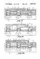
- FIGS. 1A to 1Mis a diagramatic cross-sectional representation of the processing stages of a preferred method for constructing a device in accordance with the present invention.
- FIGS. 2A and 2Bis a diagramatic cross-sectional representation depicting the formation of coaxial interconnect lines in accordance with the present invention.
- FIGS. 3A to 3His a diagramatic cross-sectional representation of the processing stages of an alternate preferred method for constructing a device in accordance with the present invention.
- FIGS. 4A to 4Dis a diagramatic cross-sectional representation of the processing stages of among alternate preferred method for constructing a device in accordance with the present invention.
- a completed semiconductor structure 10comprising a silicon substrate in which devices such as transistors and diodes have been formed. Such devices are depicted diagramatically and are identified by the reference numeral 12.
- a first dielectric layer 14is formed over the completed semiconductor 10.
- the dielectric layer 14comprises silicon dioxide which is formed during a low pressure chemical vapor deposition process (LPCVD).
- LPCVDlow pressure chemical vapor deposition process
- a reactive mixture of SiH 4 +PH 3 +O 2is used to generate glass thicknesses from 2000A to 6000A.
- An etch stop dielectric layer 16which is impervious to a first etchant (to be described subsequently), is formed over the first dielectric layer 14.
- the etch stop dielectric layer 16comprises silicon nitride, which is substantially impervious to a first etchant comprising a dilute or buffered hydrogen fluoride (HF) solution.
- the etch stop dielectric layer 16is preferably formed by low pressure chemical vapor deposition to a thickness of approximately 4000A. This layer provides good adhesion of the first metal layer with the substrate during a long exposure wet etch which is used to suspend other metal levels in free space as will be subsequently described.
- contact holes 18are etched in the etch stop dielectric layer 16 and first dielectric layer 14 in predetermined spaced relation to the device regions 12 in order to expose contact areas to associated underlying regions 12.
- the holes 18are etched using a plasma RIE process with a second etchant, preferably CHF 3 and oxygen.
- a first electrically conductive adhesion layer 20is then formed over the structure and into the contact holes 18 in contact with the device contact areas.
- the first adhesion layer 20comprise a thin (50 to 100A) titanium layer which is formed by physical vapor deposition (PVD) or sputtering and which provides good contact and adhesion to the semiconductor structure 10.
- a first electrically conductive barrier layer 22is formed over the first adhesion layer 20.
- the first barrier layer 22preferably comprises tantalum nitride (TaN), for example, which is formed by sputtering tantalum in a reactive environment of 70% Ar(g)+30% N 2 (g), to a thickness of approximately 500A.
- the barrier layer 22comprises zirconium boride (ZrB 2 ) which is formed by the reactive deposition of Zr and B.
- ZrB 2zirconium boride
- a first metal layer 24is then formed over the first barrier layer 20.
- the first metal layer 24comprises tungsten which is formed by a Chemical Vapor Deposition (CVD) process to a thickness of approximately 0.75 micron.
- the first metal layer 24is patterned with photoresist, in accordance with a predetermined first level interconnect pattern, then anisotropically etched, utilizing a plasma RIE process with a third etchant, preferably SF 6 , which stops at the etch stop dielectric layer 16 as shown in FIG. 1D.
- the third etchant SF 6reacts with the materials of the adhesion, barrier and first metal layers, 20, 22 and 24 respectively, but more slowly attacks the etch stop dielectric layer 16. Note that attack can occur; however, the dielectric layer 16 is thick enough and the attack is slow enough that the layer 16 remains continuous even after overetch.
- a first level of interconnects 26has been formed and all surfaces of the silicon dioxide material comprising the first dielectric layer 14 have been covered either by the etch stop layer dielectric 16 or the material in the contact holes 18.
- first protective dielectric layer 28is then covered with a first protective dielectric layer 28 as shown in FIG. 1E.
- the first protective layer 28is a thin layer of sputtered quartz, having a thickness of approximately 500A, which protects the underlying tungsten from oxidation during formation of an overlying second dielectric layer 30.
- the second dielectric layer 30preferably comprises a 1 micron thick film of reflow glass, such as a germanophosphosilicate glass which is formed over the protective layer 28 by atmospheric CVD deposition from a mixture of SiH 4 +PH 3 +GeH 4 +O 2 . After formation, the glass is reflowed at 950° C. to form a substantially planar upper surface.
- vias 32are opened in the planarized dielectric layer 30, preferably using photolithography to define an etch mask, then etching the openings using plasma RIE with CHF 3 and oxygen.
- the via openings 32are formed in spaced relation to the underlying first level of interconnects 26 thereby exposing predetermined contact regions thereon. Since the tungsten metallization of the first level of interconnects 26 does not form a stable oxide, it can be wet dipped in a dilute (for example 100:1) water:peroxide (H 2 O:H 2 O 2 ) solution prior to metal deposition. This substantially enhances the reliability of the contacts since there is not a stable oxide which inhibits good electrical interconnection between metal layers.
- a second adhesion layer 34is deposited over the second dielectric layer 30 into the via openings 32, in contact with the contact regions on the first level of interconnects level.
- the second adhesion layer 34comprises titanium which has been formed by physical vapor deposition (PVD) to a thickness on the order of 50 to 100A.
- PVDphysical vapor deposition
- a second metal layer 36is then deposited over the second adhesion layer 34.
- the second metal layer 36preferably comprises tungsten which is formed by chemical vapor deposition (CVD) to a thickness of approximately 7500A. It should be noted again that if a process with good tungsten adhesion is employed, it would then be possible to eliminate the tungsten adhesion layer 34.
- the via openings 32can be filled with metal using the method subsequently described for filling contacts.
- the second metal layer 36 and underlying second adhesion layer 34are then patterned using photolithographic masking techniques and etched, using plasma RIE with SF 6 to form a second level of interconnects 38 as shown in FIG. 1H.
- This structureis then covered with a second protective dielectric layer 40 and a third dielectric layer 42 as shown in FIG. 1I.
- the second protective layer 40is preferably a thin layer of sputtered quartz having a thickness of approximately 500A which protects the underlying tungsten material from oxidation during deposition of the overlying third dielectric layer 42.
- the third dielectric layer 42is preferably a thick film having a thickness of approximately 1.2um of a reflow glass such as a germanophosphosilicate glass which is formed by atmosperic CVD reaction of SiH 4 +PH 3 +GeH 4 +O 2 .
- a reflow glasssuch as a germanophosphosilicate glass which is formed by atmosperic CVD reaction of SiH 4 +PH 3 +GeH 4 +O 2 .
- the glassis then reflowed at 950° C. in order to provide a substantially planar upper surface.
- Other glasses with low reflow temperaturessuch as borophosphosilicate glasses which reflow at 850° C., can also be used.
- low temperature oxides and etch back planarizationcan be used as an alternative as previously stated.
- a second set of vias 44are then formed in the third dielectric layer 42 and second protective layer 40, in predetermined spaced relation with the underlying second level of interconnects 38 as shown in FIG. 1J.
- the second set of via openings 44are formed in accordance with the method set forth above with respect to the first set of via openings 32.
- the second set of via openings 44expose contact regions at predetermined locations on the underlying second level of interconnects 38.
- a third adhesion layer 46is then formed over the third dielectric layer 42 into the second set of via openings 44 in contact with the exposed contact regions on the second level of interconnects 36.
- the third adhesion layer 46comprises titanium which is formed by physical vapor deposition (PVD) sputtering to a thickness preferably on the order 50 to 100A.
- a third metal layer 48is then formed over the third adhesion layer 46.
- the third metal layeris preferably tungsten which is formed by chemical vapor deposition (CVD) to a thickness of approximately 7500A. As previously stated, if a process with good tungsten adhesion is employed, it is possible to eliminate the titanium adhesion layer.
- the third adhesion layer 46 and third metal layer 48are then patterned and etched, using the process previously described with respect to the formation of the second level of interconnects 38, to form a third level of interconnects 50 as shown in FIG. 1L. This process for forming additional interconnect levels can be repeated as desired to generate multi-level interconnect structures.
- this first etchantis a hydrogen fluoride (HF) bearing solution which removes the germanophosphosilicate glass and sputtered SiO 2 insulating material between all of the metal layers resulting in the structure depicted in FIG. 1M.
- the preferred etchantconsists of a mixture of 3:3:2 parts ammonium fluoride: acetic acid:water.
- a layer of insulation 52is formed around the freely supported interconnect lines of the structure depicted in FIG. 1M without filling in the gaps 53 therebetween.
- the layer of insulation 52is as thick as is reasonably necessary to ensure that gaps 53 are retained between the interconnect levels.
- the insulating layer 52comprises silicon dioxide which is deposited using a chemical vapor deposition (CVD) system to a thickness of 3000A.
- FIG. 2Ashows a cross sectional representation of layer 52 thus surrounding freely supported interconnect lines wherein layer 52 is a continuous layer coating the surfaces of the interconnect lines which are exposed when layers 30, 42 are removed. Layer 52 has inner surfaces in contact with the surfaces of the interconnect lines which were exposed prior to deposition of layer 52.
- layer 52has opposing outer surfaces 52a which are surrounded by air gaps 53 and separated by air gaps 53 from the outer surfaces 52a of other portions of layer 52.
- a layer 54 of electrically conductive materialsuch as tungsten, is formed over the insulating layer 52. It is preferred that this conductive layer 54 is formed by CVD deposition of tungsten around the gaps 53 over the insulating layer 52 thereby forming a continuous metal encapsulent around the totally isolated interconnect structure. Although gaps may be left between portions of the conductive layer 54 which surround adjacent interconnects, it is preferred that all such gaps are filled with metal thereby enhancing the mechanical strength of the structure.
- FIG. 2BThe completed structure described above is shown in FIG. 2B
- This metal layer 54can then act as a ground plane around all of the lines where it will be able to sink the field lines emanating from interconnect lines in close proximity, thereby greatly reducing their cross talk.
- the metal layer 54can also function as a heat sink. Contact pads are then cleared of metal and dielectric and the wafer is diced. Die are then packaged for die bonding. One connection to the metal layer 54 should provide close ground to all of the interconnects in the semiconductor structure. Other physical connections to the top surface of the device can be used to extract heat in the chip up through the interconnect layers.
- contact holes 18are formed in a first dielectric layer 14 and a first etch stop dielectric layer 16 over contact areas of devices 12 in the semiconductor structure 10, as previously described in conjunction with FIGS. 1A and 1B.
- a first electrically conductive layer 102comprising a first metal
- the first electrically conductive layer 102comprises aluminum which is formed to a thickness of approximately 4500A by physical sputtering.
- a second electrically conductive layer 104comprising a second metal, is formed over the first electrically conductive layer 102.
- the second electrically conductive layer 104comprises tungsten which is formed to a thickness of approximately 7500A by physical vapor deposition (PVD) or sputtering.
- the second electrically conductive layer 104is patterned into first array of posts 106 utilizing conventional photoresist techniques and an etchant which reacts with the second metal but is substantially unreactive with the first metal.
- the posts 106are metal features which protrude substantially above the electrically conductive layer 102 and which provide an electrical connection to the next metal level.
- the etching process usedis plasma RIE with SF 6 . Consequently, the first array of posts 106 are formed with the etch stopping on the first electrically conductive layer 102.
- the first electrically conductive layer 102is then patterned into a first level of interconnects 108 utilizing conventional photoresist techniques and an etchant which reacts with the first metal but which is substantially unreactive with the second metal and with the first etch stop dielectric layer 16. Consequently, the first level of interconnects 108 is formed with the etchant stopping at the first etch stop dielectric layer 16 and with the posts 106 of the first post array acting as masks against etching the underlying first metal regions. As a result, the posts 106 are self aligned with respect to the underlying first level of interconnects 108 as shown in FIG. 3C.
- a thick second dielectric layer 110is formed over the posts 106 and the first level of interconnects 108 as well as over the first etch stop dielectric layer 16.
- the second dielectric layer 110comprises a low temperature oxide which is deposited to a thickness of approximately 2 microns using low pressure chemical vapor deposition (LPCVD) of SiH 4 , PH 3 and oxygen.
- LPCVDlow pressure chemical vapor deposition
- a planarizing dielectric layer 112is then formed over the second dielectric layer 110.
- the planarizing dielectric layer 112is preferably a photoresist organic resin which is spun over the second dielectric layer 110 in order to form a substantially planar upper surface 114.
- planarizing dielectric layer 112 and second dielectric layer 110are then etched back, preferably using plasma RIE with CHF 3 +O 2 , to expose the tops of the posts 106 while maintaining a substantially planar upper surface as shown in FIG. 3F.
- the structurebe dipped into a hydrogen peroxide:water solution (1:20) to clear the exposed upper surfaces of the posts 106 of native oxide which could degrade electrical contact thereto.
- a third electrically conductive layer 116comprising the first metal which is aluminum in the preferred embodiment, is then formed on the planarized upper surface of the second insulating layer 110, into contact with the exposed tops of the posts 106.
- a fourth electrically conductive layer 118comprising the second metal which is tungsten in the preferred embodiment, is then formed over the third electrically conductive layer 116.
- the third and fourth electrically conductive layersare formed in accordance with the procedure described above with respect to the formation of the first 102 and second 104 electrically conductive layers.
- the third 116 and fourth 118 electrically conductive layerscan then be formed into a second level of interconnects and a second array of via posts respectively in accordance with the procedure described above with respect to the formation of the first level of interconnects 108 and the first array of posts 106.
- a third insulating layermay then be formed over the second level of interconnects and second array of posts planarized and etched back to expose the tops of the posts in the second array, in accordance with the procedure described above in conjunction with FIGS. 3D through 3F. These processing steps may be repeated until the desired number of interconnect levels have been formed. Subsequently, the insulating material between the interconnect lines is removed in accordance with the procedure set forth above in conjunction with FIG. 1M. Thereafter, coaxial lines can be formed as described above in conjunction with FIG. 2.
- contact holes 18are formed in a first dielectric layer 14 and a first etch stop dielectric layer 16 over contact areas of devices 12 in the semiconductor structure 10, as previously described in conjunction with FIGS. 1A and 1B.
- plugs 202comprising a first metal, preferably tungsten, are formed within the contact holes 18 as shown in FIG. 4A.
- the plugs 202are formed by selectively depositing the first metal into the contact holes 18, preferably using chemical vapor deposition (CVD).
- CVDchemical vapor deposition
- tungstenis used as the first metal and is deposited in a cold wall reactor. The substrate temperature of the wafer is held between 300° C. and 600° C.
- the deposition processis allowed to proceed until the upper surfaces of the deposited posts 202 are substantially coplanar with the upper surface of the first etch stop dielectric layer 16 as shown in FIG. 4A.
- a first metal layer 204is then formed over the first etch stop dielectric layer 16 into contact with the upper surfaces of the posts 202.
- the first metal layer 204preferably comprises tungsten or an aluminum silicon titanium sandwich alloy structure as subsequently described.
- the first metal layer 204is patterned into a first level of interconnects 205 (see FIG. 4C) utilizing conventional photoresist techniques and a etchant which reacts with the material of the first metal layer but is substantially unreactive with the material of the underlying first etch stop dielectric layer 16.
- a first protective layer, 206is formed over the first level interconnects 205 as well as the first etch stop dielectric layer 16 as previously described in conjunction with FIG. 1E.
- a planarized layer 207 of dielectric materialis formed over the first protective layer as also previously described with respect to FIG. 1E.
- a second set of vias 208are opened in the planarized dielectric layer 207 and underlying protective layer 206 preferably in accordance with the procedure previously described with respect to FIG. 1F.
- a second array of posts 210, comprising the first metal,are formed within the vias 208 in accordance with the procedure previously described with respect to FIG. 4A.
- a layer of the second metalcan then be formed over the second dielectric layer 207 into contact with the upper surfaces of the posts 210 of the second post array.
- the second metal layeris then patterned and etched to form a second level of interconnects using the second etchant. This procedure can be repeated to generate multi-level interconnect structure having the desired number of interconnect levels.
- the insulation between the interconnect linesis then removed as described above with respect to 1M.
- Coaxial interconnect linescan then be constructed in accordance with the procedure described above with respect to FIG. 2.
- the sandwich structurecomprises a first layer of an aluminum-silicon material which preferrably is 1% to 1.5% silicon by weight.
- the first aluminum-silicon layeris preferrably approximately 2500A thick.
- a first titanium layeris formed over the first aluminum-silicon layer preferrably to a thickness in a range of approximately 50A to 200A.
- At least a second aluminum-silicon layeris formed over the first titanium layer, preferrably to a thickness of approximately 2500A.
- the sandwich structurecomprises at least a first titanium layer sandwiched between at least a first and a second aluminum-silicon layer
- a second titanium layeris formed over second aluminum-silicon layer to a thickness preferrably in a range of approximately 50A to 200A.
- a third aluminum-silicon layeris formed over the second titanium layer preferrably to a thickness of approximately 2500A.
- the composition of the second and third aluminum-silicon layersis also preferrably 1% to 1.5% silicon by weight.
- a protective layeris formed over the third aluminum-silicon layer preferrably to a thickness of approximately 1000A. This sandwich structure is then patterned and etched to form the desired interconnects using methods available to those skilled in the art.
- this sandwich structuresubstantially reduces the problem of interconnect deformation such as hillocking, and resulting electrical shorts between interconnects, because the silicon in the aluminum-silicon material migrates to the titanium interface to form a ternary phase. Because of its superior mechanical strength properties over pure aluminum or standard aluminum alloys containing Cu, this sandwich structure enables the use of aluminum as the primary material for the interconnects. This is desirable due to the fact the resistance is substantially lower than that of the other materials which do not exhibit hillocking, such as tungsten. Furthermore, due to its relatively low electrical resistance properties, aluminum is less likely to cause voltage drops which affect device switching levels when compared to other high strength materials such as tungsten.
- the protective tungsten layeris desirable to prevent the formation of native oxides on the upper surface of the aluminum-silicon layer. The presence of such native oxides could cause the formation of bad electrical contacts between the interconnects and any plugs which are formed above the sandwich interconnect.
- the traditional interconnect and insulating materials of a semiconductor structurehave been replaced by a coaxial conductor system.
- the metal forming the coaxial sheathcan be made thick enough to completely fill the gaps between interconnect levels.
- the formation of coaxial interconnects with ground planeshas a distinct electrical advantage in that the all lines should have approximately the same characteristic impedance per unit length. This occurs since an ability to wrap the shield material intimately around each individual wire has been developed.
- coaxial interconnects with ground planesthat electrically shield local interconnects from crosstalk and can be used to remove thermal energy from the chip.
Landscapes
- Physics & Mathematics (AREA)
- Condensed Matter Physics & Semiconductors (AREA)
- General Physics & Mathematics (AREA)
- Engineering & Computer Science (AREA)
- Computer Hardware Design (AREA)
- Microelectronics & Electronic Packaging (AREA)
- Power Engineering (AREA)
- Internal Circuitry In Semiconductor Integrated Circuit Devices (AREA)
Abstract
Description
Claims (9)
Priority Applications (3)
| Application Number | Priority Date | Filing Date | Title |
|---|---|---|---|
| US07/393,826US4933743A (en) | 1989-03-11 | 1989-08-14 | High performance interconnect system for an integrated circuit |
| US07/525,958US5000818A (en) | 1989-08-14 | 1990-05-18 | Method of fabricating a high performance interconnect system for an integrated circuit |
| US07/610,962US5117276A (en) | 1989-08-14 | 1990-11-08 | High performance interconnect system for an integrated circuit |
Applications Claiming Priority (2)
| Application Number | Priority Date | Filing Date | Title |
|---|---|---|---|
| US2474589A | 1989-03-11 | 1989-03-11 | |
| US07/393,826US4933743A (en) | 1989-03-11 | 1989-08-14 | High performance interconnect system for an integrated circuit |
Related Parent Applications (1)
| Application Number | Title | Priority Date | Filing Date |
|---|---|---|---|
| US2474589AContinuation | 1989-03-11 | 1989-03-11 |
Related Child Applications (1)
| Application Number | Title | Priority Date | Filing Date |
|---|---|---|---|
| US07/525,958DivisionUS5000818A (en) | 1989-08-14 | 1990-05-18 | Method of fabricating a high performance interconnect system for an integrated circuit |
Publications (1)
| Publication Number | Publication Date |
|---|---|
| US4933743Atrue US4933743A (en) | 1990-06-12 |
Family
ID=26698820
Family Applications (1)
| Application Number | Title | Priority Date | Filing Date |
|---|---|---|---|
| US07/393,826Expired - LifetimeUS4933743A (en) | 1989-03-11 | 1989-08-14 | High performance interconnect system for an integrated circuit |
Country Status (1)
| Country | Link |
|---|---|
| US (1) | US4933743A (en) |
Cited By (109)
| Publication number | Priority date | Publication date | Assignee | Title |
|---|---|---|---|---|
| US5144228A (en)* | 1991-04-23 | 1992-09-01 | International Business Machines Corporation | Probe interface assembly |
| US5148260A (en)* | 1989-09-07 | 1992-09-15 | Kabushiki Kaisha Toshiba | Semiconductor device having an improved air-bridge lead structure |
| US5229643A (en)* | 1990-07-25 | 1993-07-20 | Hitachi, Ltd. | Semiconductor apparatus and semiconductor package |
| US5250847A (en)* | 1991-06-27 | 1993-10-05 | Motorola, Inc. | Stress isolating signal path for integrated circuits |
| US5264728A (en)* | 1989-11-30 | 1993-11-23 | Kabushiki Kaisha Toshiba | Line material, electronic device using the line material and liquid crystal display |
| US5306952A (en)* | 1991-10-14 | 1994-04-26 | Mitsubishi Denki Kabushiki Kaisha | Multilayer aluminum-containing interconnection structure of semiconductor device |
| US5319237A (en)* | 1990-03-09 | 1994-06-07 | Thomson Composants Microondes | Power semiconductor component |
| GB2274200A (en)* | 1991-10-29 | 1994-07-13 | Gen Electric | A High density interconnect structure including a spacer structure and a gap |
| US5444015A (en)* | 1992-12-15 | 1995-08-22 | International Business Machines Corporation | Larce scale IC personalization method employing air dielectric structure for extended conductors |
| US5446243A (en)* | 1992-05-20 | 1995-08-29 | International Business Machines Corporation | Post processing shielding |
| US5453154A (en)* | 1991-10-21 | 1995-09-26 | National Semiconductor Corporation | Method of making an integrated circuit microwave interconnect and components |
| US5471093A (en)* | 1994-10-28 | 1995-11-28 | Advanced Micro Devices, Inc. | Pseudo-low dielectric constant technology |
| US5482897A (en)* | 1994-07-19 | 1996-01-09 | Lsi Logic Corporation | Integrated circuit with on-chip ground plane |
| US5496771A (en)* | 1994-05-19 | 1996-03-05 | International Business Machines Corporation | Method of making overpass mask/insulator for local interconnects |
| US5502334A (en)* | 1992-11-10 | 1996-03-26 | Sony Corporation | Metal wiring |
| US5514622A (en)* | 1994-08-29 | 1996-05-07 | Cypress Semiconductor Corporation | Method for the formation of interconnects and landing pads having a thin, conductive film underlying the plug or an associated contact of via hole |
| US5532518A (en)* | 1994-11-22 | 1996-07-02 | International Business Machines Corporation | Electrical connect and method of fabrication for semiconductor cube technology |
| US5539227A (en)* | 1993-11-24 | 1996-07-23 | Mitsubishi Denki Kabushiki Kaisha | Multi-layer wiring |
| US5584891A (en)* | 1996-01-18 | 1996-12-17 | Micron Communications, Inc. | Methods of forming a button-type battery terminal housing member sheet and of forming button-type batteries |
| US5625232A (en)* | 1994-07-15 | 1997-04-29 | Texas Instruments Incorporated | Reliability of metal leads in high speed LSI semiconductors using dummy vias |
| US5670828A (en)* | 1995-02-21 | 1997-09-23 | Advanced Micro Devices, Inc. | Tunneling technology for reducing intra-conductive layer capacitance |
| US5677574A (en)* | 1995-04-12 | 1997-10-14 | Mitsubishi Denki Kabushiki Kaisha | Airbridge wiring structure for MMIC |
| US5736863A (en)* | 1996-06-19 | 1998-04-07 | Taiwan Semiconductor Manufacturing Company, Ltd. | Abatement of electron beam charging distortion during dimensional measurements of integrated circuit patterns with scanning electron microscopy by the utilization of specially designed test structures |
| US5793112A (en)* | 1996-04-11 | 1998-08-11 | Mitsubishi Denki Kabushiki Kaisha | Multilevel embedded wiring system |
| US5835112A (en)* | 1996-10-08 | 1998-11-10 | Hewlett-Packard Company | Segmented electrical distribution plane |
| US5861676A (en)* | 1996-11-27 | 1999-01-19 | Cypress Semiconductor Corp. | Method of forming robust interconnect and contact structures in a semiconductor and/or integrated circuit |
| US5892281A (en)* | 1996-06-10 | 1999-04-06 | Micron Technology, Inc. | Tantalum-aluminum-nitrogen material for semiconductor devices |
| US5897371A (en)* | 1996-12-19 | 1999-04-27 | Cypress Semiconductor Corp. | Alignment process compatible with chemical mechanical polishing |
| US5945897A (en)* | 1998-04-30 | 1999-08-31 | Lockheed Martin Corporation | Compliant RF coaxial interconnect |
| WO1999054934A1 (en)* | 1998-04-22 | 1999-10-28 | Cvc Products, Inc. | Ultra high-speed chip interconnect using free-space dielectrics |
| US5977638A (en)* | 1996-11-21 | 1999-11-02 | Cypress Semiconductor Corp. | Edge metal for interconnect layers |
| US6016000A (en)* | 1998-04-22 | 2000-01-18 | Cvc, Inc. | Ultra high-speed chip semiconductor integrated circuit interconnect structure and fabrication method using free-space dielectrics |
| US6025260A (en)* | 1998-02-05 | 2000-02-15 | Integrated Device Technology, Inc. | Method for fabricating air gap with borderless contact |
| US6031188A (en)* | 1998-04-30 | 2000-02-29 | Lockheed Martin Corp. | Multi-circuit RF connections using molded and compliant RF coaxial interconnects |
| US6060383A (en)* | 1998-08-10 | 2000-05-09 | Nogami; Takeshi | Method for making multilayered coaxial interconnect structure |
| US6081988A (en)* | 1998-04-30 | 2000-07-04 | Lockheed Martin Corp. | Fabrication of a circuit module with a coaxial transmission line |
| US6096636A (en)* | 1996-02-06 | 2000-08-01 | Micron Technology, Inc. | Methods of forming conductive lines |
| US6130151A (en)* | 1999-05-07 | 2000-10-10 | Taiwan Semiconductor Manufacturing Company | Method of manufacturing air gap in multilevel interconnection |
| US6140023A (en)* | 1998-12-01 | 2000-10-31 | Advanced Micro Devices, Inc. | Method for transferring patterns created by lithography |
| US6143616A (en)* | 1997-08-22 | 2000-11-07 | Micron Technology, Inc. | Methods of forming coaxial integrated circuitry interconnect lines |
| US6156630A (en)* | 1997-08-22 | 2000-12-05 | Micron Technology, Inc. | Titanium boride gate electrode and interconnect and methods regarding same |
| US6174803B1 (en)* | 1998-09-16 | 2001-01-16 | Vsli Technology | Integrated circuit device interconnection techniques |
| US6187677B1 (en) | 1997-08-22 | 2001-02-13 | Micron Technology, Inc. | Integrated circuitry and methods of forming integrated circuitry |
| US6232664B1 (en)* | 1998-05-28 | 2001-05-15 | Fujitsu Limited | Semiconductor device having A1 alloy wiring |
| US6294455B1 (en) | 1997-08-20 | 2001-09-25 | Micron Technology, Inc. | Conductive lines, coaxial lines, integrated circuitry, and methods of forming conductive lines, coaxial lines, and integrated circuitry |
| EP1155447A2 (en)* | 1999-02-15 | 2001-11-21 | Infineon Technologies AG | Semiconductor structure with a strip conductor |
| US6333255B1 (en) | 1997-08-21 | 2001-12-25 | Matsushita Electronics Corporation | Method for making semiconductor device containing low carbon film for interconnect structures |
| US6373740B1 (en) | 1999-07-30 | 2002-04-16 | Micron Technology, Inc. | Transmission lines for CMOS integrated circuits |
| US6380625B2 (en) | 1999-01-13 | 2002-04-30 | Advanced Micro Devices, Inc. | Semiconductor interconnect barrier and manufacturing method thereof |
| US6388198B1 (en) | 1999-03-09 | 2002-05-14 | International Business Machines Corporation | Coaxial wiring within SOI semiconductor, PCB to system for high speed operation and signal quality |
| US6399512B1 (en) | 2000-06-15 | 2002-06-04 | Cypress Semiconductor Corporation | Method of making metallization and contact structures in an integrated circuit comprising an etch stop layer |
| US20020100685A1 (en)* | 1999-11-11 | 2002-08-01 | Apex Biotechnology Corporation | Biosensor with multiple sampling ways |
| US6441490B1 (en)* | 2000-12-18 | 2002-08-27 | Advanced Micro Devices, Inc. | Low dielectric constant stop layer for integrated circuit interconnects |
| US20020177302A1 (en)* | 2000-01-18 | 2002-11-28 | Micron Technology, Inc. | Structures and methods to enhance copper metallization |
| US6541860B1 (en)* | 2001-06-05 | 2003-04-01 | Advanced Micro Devices, Inc. | Barrier-to-seed layer alloying in integrated circuit interconnects |
| US6545358B2 (en)* | 1998-09-16 | 2003-04-08 | Samsung Electronics, Co., Ltd. | Integrated circuits having plugs in conductive layers therein and related methods |
| US6576976B2 (en) | 1997-01-03 | 2003-06-10 | Integrated Device Technology, Inc. | Semiconductor integrated circuit with an insulation structure having reduced permittivity |
| US6582976B2 (en)* | 2001-10-11 | 2003-06-24 | Fujitsu Limited | Semiconductor device manufacturing method capable of reliable inspection for hole opening and semiconductor devices manufactured by the method |
| US6614098B1 (en)* | 1989-04-07 | 2003-09-02 | Inmos Limited | Semiconductor devices and fabrication thereof |
| US20030176053A1 (en)* | 2002-03-13 | 2003-09-18 | Micron Technology, Inc. | High permeability thin films and patterned thin films to reduce noise in high speed interconnections |
| US20030176028A1 (en)* | 2002-03-13 | 2003-09-18 | Micron Technology, Inc. | High permeability composite films to reduce noise in high speed interconnects |
| US6627547B2 (en) | 1996-08-01 | 2003-09-30 | Cypress Semiconductor Corporation | Hot metallization process |
| US6635566B1 (en) | 2000-06-15 | 2003-10-21 | Cypress Semiconductor Corporation | Method of making metallization and contact structures in an integrated circuit |
| US6693361B1 (en)* | 1999-12-06 | 2004-02-17 | Tru-Si Technologies, Inc. | Packaging of integrated circuits and vertical integration |
| US6720655B1 (en)* | 1997-06-13 | 2004-04-13 | Micron Technology, Inc. | Multilevel interconnect structure with low-k dielectric |
| US20040092094A1 (en)* | 2001-12-28 | 2004-05-13 | Husher John Durbin | Integrated device technology using a buried power buss for major device and circuit advantages |
| US6737887B2 (en) | 1999-02-09 | 2004-05-18 | Micron Technology, Inc. | Current mode signal interconnects and CMOS amplifier |
| US6815358B2 (en) | 2001-09-06 | 2004-11-09 | Seagate Technology Llc | Electron beam lithography method for plating sub-100 nm trenches |
| US20040233010A1 (en)* | 2003-05-22 | 2004-11-25 | Salman Akram | Atomic layer deposition (ALD) high permeability layered magnetic films to reduce noise in high speed interconnection |
| US20050023697A1 (en)* | 2000-01-18 | 2005-02-03 | Micron Technology, Inc. | Methods for making integrated-circuit wiring from copper, silver, gold, and other metals |
| US20050023650A1 (en)* | 2002-01-30 | 2005-02-03 | Micron Technology, Inc. | Capacitive techniques to reduce noise in high speed interconnections |
| US20050030803A1 (en)* | 2002-03-13 | 2005-02-10 | Micron Technology, Inc. | High permeability layered films to reduce noise in high speed interconnects |
| US6882053B1 (en)* | 2001-12-28 | 2005-04-19 | Micrel, Inc. | Buried power buss utilized as a ground strap for high current, high power semiconductor devices and a method for providing the same |
| US20050087871A1 (en)* | 2003-10-24 | 2005-04-28 | Kazuhide Abe | Wiring structure of semiconductor device and production method of the device |
| US20050087872A1 (en)* | 2003-10-28 | 2005-04-28 | Kazuhide Abe | Wiring structure of semiconductor device and method of manufacturing the same |
| US6894393B1 (en) | 2001-12-28 | 2005-05-17 | Micrel, Inc. | Buried power bus utilized as a sinker for high current, high power semiconductor devices and a method for providing the same |
| US20050205941A1 (en)* | 2004-03-17 | 2005-09-22 | Nissan Motor Co., Ltd. | Heat resistant ohmic electrode and method of manufacturing the same |
| US7049219B1 (en) | 2002-11-08 | 2006-05-23 | Micron Technology, Inc. | Coating of copper and silver air bridge structures to improve electromigration resistance and other applications |
| US20060131702A1 (en)* | 1999-07-30 | 2006-06-22 | Micron Technology, Inc. | Novel transmission lines for CMOS integrated circuits |
| US7067421B2 (en) | 2000-05-31 | 2006-06-27 | Micron Technology, Inc. | Multilevel copper interconnect with double passivation |
| US20060216861A1 (en)* | 2005-03-25 | 2006-09-28 | Fujitsu Limited | Manufacturing method of wiring substrate |
| US20070040274A1 (en)* | 2005-08-22 | 2007-02-22 | Cheng-Shih Lee | Interconnect of group iii- v semiconductor device and fabrication method for making the same |
| US7262505B2 (en)* | 2000-01-18 | 2007-08-28 | Micron Technology, Inc. | Selective electroless-plated copper metallization |
| US7285196B2 (en) | 2000-01-18 | 2007-10-23 | Micron Technology, Inc. | Methods and apparatus for making integrated-circuit wiring from copper, silver, gold, and other metals |
| US20080166874A1 (en)* | 2007-01-05 | 2008-07-10 | International Business Machines Corporation | Formation of vertical devices by electroplating |
| US7405454B2 (en) | 2003-03-04 | 2008-07-29 | Micron Technology, Inc. | Electronic apparatus with deposited dielectric layers |
| US20080197398A1 (en)* | 2007-02-19 | 2008-08-21 | Toshiaki Komukai | Semiconductor device and method of manufacturing the same |
| US20080251924A1 (en)* | 2003-10-15 | 2008-10-16 | Megica Corporation | Post Passivation Interconnection Schemes On Top Of The IC Chips |
| US20090033351A1 (en)* | 2007-07-30 | 2009-02-05 | International Business Machines Corporation | Test structure for electromigration analysis and related method |
| US20090160062A1 (en)* | 2007-12-19 | 2009-06-25 | Park O Seo | Semiconductor Devices and Methods of Manufacturing Thereof |
| US7560793B2 (en) | 2002-05-02 | 2009-07-14 | Micron Technology, Inc. | Atomic layer deposition and conversion |
| US7670646B2 (en) | 2002-05-02 | 2010-03-02 | Micron Technology, Inc. | Methods for atomic-layer deposition |
| US7915721B2 (en) | 2008-03-12 | 2011-03-29 | Fairchild Semiconductor Corporation | Semiconductor die package including IC driver and bridge |
| US8129266B2 (en) | 2008-07-09 | 2012-03-06 | Semiconductor Componenets Industries, LLC | Method of forming a shielded semiconductor device and structure therefor |
| US20120074508A1 (en)* | 2006-03-22 | 2012-03-29 | Mitsubishi Electric Corporation | Power semiconductor device |
| CN102593046A (en)* | 2010-12-22 | 2012-07-18 | 通用电气公司 | Method for fabricating a semiconductor device package |
| US20120193795A1 (en)* | 2011-01-31 | 2012-08-02 | Avago Technologies Wireless Ip (Singapore) Pte. Ltd. | Semiconductor device having an airbridge and method of fabricating the same |
| US20120292763A1 (en)* | 2010-02-09 | 2012-11-22 | International Business Machines Corporation | Electromigration immune through-substrate vias |
| US20130087365A1 (en)* | 2011-10-05 | 2013-04-11 | Harris Corporation | Method for making electrical structure with air dielectric and related electrical structures |
| US8501563B2 (en) | 2005-07-20 | 2013-08-06 | Micron Technology, Inc. | Devices with nanocrystals and methods of formation |
| US8796904B2 (en) | 2011-10-31 | 2014-08-05 | Avago Technologies General Ip (Singapore) Pte. Ltd. | Bulk acoustic resonator comprising piezoelectric layer and inverse piezoelectric layer |
| US8981876B2 (en) | 2004-11-15 | 2015-03-17 | Avago Technologies General Ip (Singapore) Pte. Ltd. | Piezoelectric resonator structures and electrical filters having frame elements |
| US9243316B2 (en) | 2010-01-22 | 2016-01-26 | Avago Technologies General Ip (Singapore) Pte. Ltd. | Method of fabricating piezoelectric material with selected c-axis orientation |
| US9385684B2 (en) | 2012-10-23 | 2016-07-05 | Avago Technologies General Ip (Singapore) Pte. Ltd. | Acoustic resonator having guard ring |
| US9401692B2 (en) | 2012-10-29 | 2016-07-26 | Avago Technologies General Ip (Singapore) Pte. Ltd. | Acoustic resonator having collar structure |
| US9490771B2 (en) | 2012-10-29 | 2016-11-08 | Avago Technologies General Ip (Singapore) Pte. Ltd. | Acoustic resonator comprising collar and frame |
| US9490418B2 (en) | 2011-03-29 | 2016-11-08 | Avago Technologies General Ip (Singapore) Pte. Ltd. | Acoustic resonator comprising collar and acoustic reflector with temperature compensating layer |
| US20170213786A1 (en)* | 2016-01-27 | 2017-07-27 | Samsung Electronics Co., Ltd. | Semiconductor device and method of manufacturing the same |
| US20180350673A1 (en)* | 2017-05-31 | 2018-12-06 | United Microelectronics Corp. | Method of forming a semiconductor structure |
Citations (17)
| Publication number | Priority date | Publication date | Assignee | Title |
|---|---|---|---|---|
| US4045594A (en)* | 1975-12-31 | 1977-08-30 | Ibm Corporation | Planar insulation of conductive patterns by chemical vapor deposition and sputtering |
| US4097889A (en)* | 1976-11-01 | 1978-06-27 | Rca Corporation | Combination glass/low temperature deposited Siw Nx Hy O.sub.z |
| US4527184A (en)* | 1982-12-01 | 1985-07-02 | Siemens Aktiengesellschaft | Integrated semiconductor circuits with contact interconnect levels comprised of an aluminum/silicon alloy |
| US4556897A (en)* | 1982-02-09 | 1985-12-03 | Nippon Electric Co., Ltd. | Titanium coated aluminum leads |
| US4566940A (en)* | 1981-04-21 | 1986-01-28 | Nippon Telegraph And Telephone Public Corporation | Manufacturing process for semiconductor integrated circuits |
| US4601915A (en)* | 1984-09-24 | 1986-07-22 | Motorola, Inc. | Method of fabricating air supported crossovers |
| US4601781A (en)* | 1984-06-15 | 1986-07-22 | Northern Telecom Limited | Method for improving step coverage of dielectrics in VLSI circuits |
| EP0194950A2 (en)* | 1985-03-15 | 1986-09-17 | Fairchild Semiconductor Corporation | High temperature interconnect system for an integrated circuit |
| US4617193A (en)* | 1983-06-16 | 1986-10-14 | Digital Equipment Corporation | Planar interconnect for integrated circuits |
| US4632725A (en)* | 1984-03-19 | 1986-12-30 | Commissariat A L'energie Atomique | Method for interconnecting the active zones and/or the gates of a C/MOS integrated circuit |
| US4659427A (en)* | 1984-12-31 | 1987-04-21 | Gte Laboratories Incorporated | Via formation for multilayered metalization |
| US4680610A (en)* | 1983-11-30 | 1987-07-14 | Siemens Aktiengesellschaft | Semiconductor component comprising bump-like, metallic lead contacts and multilayer wiring |
| US4689113A (en)* | 1986-03-21 | 1987-08-25 | International Business Machines Corporation | Process for forming planar chip-level wiring |
| US4694317A (en)* | 1984-10-22 | 1987-09-15 | Fuji Photo Film Co., Ltd. | Solid state imaging device and process for fabricating the same |
| EP0239489A2 (en)* | 1986-03-24 | 1987-09-30 | Fairchild Semiconductor Corporation | A process for forming vias on integrated circuits |
| US4761677A (en)* | 1981-09-18 | 1988-08-02 | Fujitsu Limited | Semiconductor device having new conductive interconnection structure and method for manufacturing the same |
| US4783695A (en)* | 1986-09-26 | 1988-11-08 | General Electric Company | Multichip integrated circuit packaging configuration and method |
- 1989
- 1989-08-14USUS07/393,826patent/US4933743A/ennot_activeExpired - Lifetime
Patent Citations (17)
| Publication number | Priority date | Publication date | Assignee | Title |
|---|---|---|---|---|
| US4045594A (en)* | 1975-12-31 | 1977-08-30 | Ibm Corporation | Planar insulation of conductive patterns by chemical vapor deposition and sputtering |
| US4097889A (en)* | 1976-11-01 | 1978-06-27 | Rca Corporation | Combination glass/low temperature deposited Siw Nx Hy O.sub.z |
| US4566940A (en)* | 1981-04-21 | 1986-01-28 | Nippon Telegraph And Telephone Public Corporation | Manufacturing process for semiconductor integrated circuits |
| US4761677A (en)* | 1981-09-18 | 1988-08-02 | Fujitsu Limited | Semiconductor device having new conductive interconnection structure and method for manufacturing the same |
| US4556897A (en)* | 1982-02-09 | 1985-12-03 | Nippon Electric Co., Ltd. | Titanium coated aluminum leads |
| US4527184A (en)* | 1982-12-01 | 1985-07-02 | Siemens Aktiengesellschaft | Integrated semiconductor circuits with contact interconnect levels comprised of an aluminum/silicon alloy |
| US4617193A (en)* | 1983-06-16 | 1986-10-14 | Digital Equipment Corporation | Planar interconnect for integrated circuits |
| US4680610A (en)* | 1983-11-30 | 1987-07-14 | Siemens Aktiengesellschaft | Semiconductor component comprising bump-like, metallic lead contacts and multilayer wiring |
| US4632725A (en)* | 1984-03-19 | 1986-12-30 | Commissariat A L'energie Atomique | Method for interconnecting the active zones and/or the gates of a C/MOS integrated circuit |
| US4601781A (en)* | 1984-06-15 | 1986-07-22 | Northern Telecom Limited | Method for improving step coverage of dielectrics in VLSI circuits |
| US4601915A (en)* | 1984-09-24 | 1986-07-22 | Motorola, Inc. | Method of fabricating air supported crossovers |
| US4694317A (en)* | 1984-10-22 | 1987-09-15 | Fuji Photo Film Co., Ltd. | Solid state imaging device and process for fabricating the same |
| US4659427A (en)* | 1984-12-31 | 1987-04-21 | Gte Laboratories Incorporated | Via formation for multilayered metalization |
| EP0194950A2 (en)* | 1985-03-15 | 1986-09-17 | Fairchild Semiconductor Corporation | High temperature interconnect system for an integrated circuit |
| US4689113A (en)* | 1986-03-21 | 1987-08-25 | International Business Machines Corporation | Process for forming planar chip-level wiring |
| EP0239489A2 (en)* | 1986-03-24 | 1987-09-30 | Fairchild Semiconductor Corporation | A process for forming vias on integrated circuits |
| US4783695A (en)* | 1986-09-26 | 1988-11-08 | General Electric Company | Multichip integrated circuit packaging configuration and method |
Non-Patent Citations (18)
| Title |
|---|
| "Plasma Planarization", Solid State Transactions, vol. 24, No. 4, Apr. 1981, A. C. Adams. |
| Article entitled "A GaAs MSI 8-bit Multiplexer and Demultiplexer" by McCormack et al., pp. 25-28, GaAs IC Symposium, publication number CH1764-0/82/0000-0025, 1982 IEEE. |
| Article entitled "A High Yield GaAs Array Technology and Applications", by Rode et al., pp. 178-181, GaAs IC Symposium, publication number CH1876-2/83/0000-0178, 1983 IEEE. |
| Article entitled "Air-Bridge Microbolometer for Far-Infrared Detection", by Neikirk et al.; pp. 153-155, American Institute of Physics, Appl. Phys. Lett 44(2), Jan. 15, 1984. |
| Article entitled "Analysis of Crosstalk in Very High-Speed LSI/VLSI's Using a Coupled Multiconductor MIS Microstrip Line Model", by Seki et al., pp. 1948-1953, IEEE Transactions on Electron Devices, vol. Ed-31, No. 12, Dec. 1984. |
| Article entitled "Analysis of Interconnection Delay on Very High-Speed LSI/VLSI Chips Using an MIS Microstrip Line Model", by Hasegawa et al., pp. 1954-1960, IEEE Transaction on Electron Devices, vol. Ed-31, No. 12, Dec. 1984. |
| Article entitled "Effects of Capacitance at Crossover Wirings in Power GaAs M.E.S.F.E.T.S", by Aono et al., pp. 417-418, Electronics Letters, May 22nd, 1980, vol. 16, No. 11. |
| Article entitled "Effects of Interconnections on Submicron Chip Performance", by Carter et al.; pp. 63-68, VLSI Design, Jan. 1984. |
| Article entitled "Glass Reinforced GaAs Beam Lead Schottky Diode with Airbridge for Millimetre Wavelengths", by Mills et al.; pp. 787-788, Electronics Letters, Sep. 13th, 1984, vol. 20, No. 19. |
| Article entitled A GaAs MSI 8 bit Multiplexer and Demultiplexer by McCormack et al., pp. 25 28, GaAs IC Symposium, publication number CH1764 0/82/0000 0025, 1982 IEEE.* |
| Article entitled A High Yield GaAs Array Technology and Applications , by Rode et al., pp. 178 181, GaAs IC Symposium, publication number CH1876 2/83/0000 0178, 1983 IEEE.* |
| Article entitled Air Bridge Microbolometer for Far Infrared Detection , by Neikirk et al.; pp. 153 155, American Institute of Physics, Appl. Phys. Lett 44(2), Jan. 15, 1984.* |
| Article entitled Analysis of Crosstalk in Very High Speed LSI/VLSI s Using a Coupled Multiconductor MIS Microstrip Line Model , by Seki et al., pp. 1948 1953, IEEE Transactions on Electron Devices, vol. Ed 31, No. 12, Dec. 1984.* |
| Article entitled Analysis of Interconnection Delay on Very High Speed LSI/VLSI Chips Using an MIS Microstrip Line Model , by Hasegawa et al., pp. 1954 1960, IEEE Transaction on Electron Devices, vol. Ed 31, No. 12, Dec. 1984.* |
| Article entitled Effects of Capacitance at Crossover Wirings in Power GaAs M.E.S.F.E.T.S , by Aono et al., pp. 417 418, Electronics Letters, May 22nd, 1980, vol. 16, No. 11.* |
| Article entitled Effects of Interconnections on Submicron Chip Performance , by Carter et al.; pp. 63 68, VLSI Design, Jan. 1984.* |
| Article entitled Glass Reinforced GaAs Beam Lead Schottky Diode with Airbridge for Millimetre Wavelengths , by Mills et al.; pp. 787 788, Electronics Letters, Sep. 13th, 1984, vol. 20, No. 19.* |
| Plasma Planarization , Solid State Transactions, vol. 24, No. 4, Apr. 1981, A. C. Adams.* |
Cited By (242)
| Publication number | Priority date | Publication date | Assignee | Title |
|---|---|---|---|---|
| US6614098B1 (en)* | 1989-04-07 | 2003-09-02 | Inmos Limited | Semiconductor devices and fabrication thereof |
| US5148260A (en)* | 1989-09-07 | 1992-09-15 | Kabushiki Kaisha Toshiba | Semiconductor device having an improved air-bridge lead structure |
| US5428250A (en)* | 1989-11-30 | 1995-06-27 | Kabushiki Kaisha Toshiba | Line material, electronic device using the line material and liquid crystal display |
| US5264728A (en)* | 1989-11-30 | 1993-11-23 | Kabushiki Kaisha Toshiba | Line material, electronic device using the line material and liquid crystal display |
| US5319237A (en)* | 1990-03-09 | 1994-06-07 | Thomson Composants Microondes | Power semiconductor component |
| US5229643A (en)* | 1990-07-25 | 1993-07-20 | Hitachi, Ltd. | Semiconductor apparatus and semiconductor package |
| US5144228A (en)* | 1991-04-23 | 1992-09-01 | International Business Machines Corporation | Probe interface assembly |
| US5250847A (en)* | 1991-06-27 | 1993-10-05 | Motorola, Inc. | Stress isolating signal path for integrated circuits |
| US5420070A (en)* | 1991-10-14 | 1995-05-30 | Mitsubishi Denki Kabushiki Kaisha | Manufacturing method of interconnection structure of semiconductor device |
| US5306952A (en)* | 1991-10-14 | 1994-04-26 | Mitsubishi Denki Kabushiki Kaisha | Multilayer aluminum-containing interconnection structure of semiconductor device |
| US5453154A (en)* | 1991-10-21 | 1995-09-26 | National Semiconductor Corporation | Method of making an integrated circuit microwave interconnect and components |
| GB2274200B (en)* | 1991-10-29 | 1996-03-20 | Gen Electric | A high density interconnect structure including a spacer structure and a gap |
| GB2274200A (en)* | 1991-10-29 | 1994-07-13 | Gen Electric | A High density interconnect structure including a spacer structure and a gap |
| US5446243A (en)* | 1992-05-20 | 1995-08-29 | International Business Machines Corporation | Post processing shielding |
| US5502334A (en)* | 1992-11-10 | 1996-03-26 | Sony Corporation | Metal wiring |
| US5444015A (en)* | 1992-12-15 | 1995-08-22 | International Business Machines Corporation | Larce scale IC personalization method employing air dielectric structure for extended conductors |
| US5539227A (en)* | 1993-11-24 | 1996-07-23 | Mitsubishi Denki Kabushiki Kaisha | Multi-layer wiring |
| US5496771A (en)* | 1994-05-19 | 1996-03-05 | International Business Machines Corporation | Method of making overpass mask/insulator for local interconnects |
| US5625232A (en)* | 1994-07-15 | 1997-04-29 | Texas Instruments Incorporated | Reliability of metal leads in high speed LSI semiconductors using dummy vias |
| US5675187A (en)* | 1994-07-15 | 1997-10-07 | Texas Instruments Incorporated | Reliability of metal leads in high speed LSI semiconductors using dummy vias |
| US5482897A (en)* | 1994-07-19 | 1996-01-09 | Lsi Logic Corporation | Integrated circuit with on-chip ground plane |
| US5514622A (en)* | 1994-08-29 | 1996-05-07 | Cypress Semiconductor Corporation | Method for the formation of interconnects and landing pads having a thin, conductive film underlying the plug or an associated contact of via hole |
| US5471093A (en)* | 1994-10-28 | 1995-11-28 | Advanced Micro Devices, Inc. | Pseudo-low dielectric constant technology |
| US5532518A (en)* | 1994-11-22 | 1996-07-02 | International Business Machines Corporation | Electrical connect and method of fabrication for semiconductor cube technology |
| US5670828A (en)* | 1995-02-21 | 1997-09-23 | Advanced Micro Devices, Inc. | Tunneling technology for reducing intra-conductive layer capacitance |
| US5677574A (en)* | 1995-04-12 | 1997-10-14 | Mitsubishi Denki Kabushiki Kaisha | Airbridge wiring structure for MMIC |
| US5584891A (en)* | 1996-01-18 | 1996-12-17 | Micron Communications, Inc. | Methods of forming a button-type battery terminal housing member sheet and of forming button-type batteries |
| US5676709A (en)* | 1996-01-18 | 1997-10-14 | Micron Communications, Inc. | Method of forming battery terminal housing members and battery terminal housing member sheets |
| US6096636A (en)* | 1996-02-06 | 2000-08-01 | Micron Technology, Inc. | Methods of forming conductive lines |
| US20050009326A1 (en)* | 1996-02-06 | 2005-01-13 | Monte Manning | Integrated circuitry and a semiconductor processing method of forming a series of conductive lines |
| US7208836B2 (en) | 1996-02-06 | 2007-04-24 | Micron Technology, Inc. | Integrated circuitry and a semiconductor processing method of forming a series of conductive lines |
| US20050035456A1 (en)* | 1996-02-06 | 2005-02-17 | Micron Technology, Inc. | Integrated circuitry and a semiconductor processing method of forming a series of conductive lines |
| US6611059B1 (en) | 1996-02-06 | 2003-08-26 | Micron Technology, Inc. | Integrated circuitry conductive lines |
| US7148134B2 (en) | 1996-02-06 | 2006-12-12 | Micron Technology, Inc. | Integrated circuitry and a semiconductor processing method of forming a series of conductive lines |
| US5793112A (en)* | 1996-04-11 | 1998-08-11 | Mitsubishi Denki Kabushiki Kaisha | Multilevel embedded wiring system |
| US6184124B1 (en) | 1996-04-11 | 2001-02-06 | Mitsubishi Denki Kabushiki Kaisha | Method of making embedded wiring system |
| US6913997B2 (en) | 1996-06-10 | 2005-07-05 | Micron Technology, Inc. | Method of using tantalum-aluminum-nitrogen material as diffusion barrier and adhesion layer in semiconductor devices |
| US6611061B2 (en) | 1996-06-10 | 2003-08-26 | Micron Technology, Inc. | Tantalum-aluminum-nitrogen material for semiconductor devices |
| US5892281A (en)* | 1996-06-10 | 1999-04-06 | Micron Technology, Inc. | Tantalum-aluminum-nitrogen material for semiconductor devices |
| US6432818B1 (en) | 1996-06-10 | 2002-08-13 | Micron Technology, Inc. | Method of using tantalum-aluminum-nitrogen material as diffusion barrier and adhesion layer in semiconductor devices |
| US6404057B1 (en) | 1996-06-10 | 2002-06-11 | Micron Technology, Inc. | Tantalum - aluminum - nitrogen material for semiconductor devices |
| US6133636A (en)* | 1996-06-10 | 2000-10-17 | Micron Technology, Inc. | Tantalum-aluminum-nitrogen material for semiconductor devices |
| US5736863A (en)* | 1996-06-19 | 1998-04-07 | Taiwan Semiconductor Manufacturing Company, Ltd. | Abatement of electron beam charging distortion during dimensional measurements of integrated circuit patterns with scanning electron microscopy by the utilization of specially designed test structures |
| US6627547B2 (en) | 1996-08-01 | 2003-09-30 | Cypress Semiconductor Corporation | Hot metallization process |
| US5835112A (en)* | 1996-10-08 | 1998-11-10 | Hewlett-Packard Company | Segmented electrical distribution plane |
| US5977638A (en)* | 1996-11-21 | 1999-11-02 | Cypress Semiconductor Corp. | Edge metal for interconnect layers |
| US5861676A (en)* | 1996-11-27 | 1999-01-19 | Cypress Semiconductor Corp. | Method of forming robust interconnect and contact structures in a semiconductor and/or integrated circuit |
| US5897371A (en)* | 1996-12-19 | 1999-04-27 | Cypress Semiconductor Corp. | Alignment process compatible with chemical mechanical polishing |
| US6576976B2 (en) | 1997-01-03 | 2003-06-10 | Integrated Device Technology, Inc. | Semiconductor integrated circuit with an insulation structure having reduced permittivity |
| US20040150109A1 (en)* | 1997-06-13 | 2004-08-05 | Ahn Kie Y. | Multilevel interconnect structure with low-k dielectric |
| US6720655B1 (en)* | 1997-06-13 | 2004-04-13 | Micron Technology, Inc. | Multilevel interconnect structure with low-k dielectric |
| US7138718B2 (en)* | 1997-06-13 | 2006-11-21 | Micron Technology, Inc. | Multilevel interconnect structure with low-k dielectric |
| US6774491B2 (en) | 1997-08-20 | 2004-08-10 | Micron Technology, Inc. | Conductive lines, coaxial lines, integrated circuitry, and methods of forming conductive lines, coaxial lines, and integrated circuitry |
| US6294455B1 (en) | 1997-08-20 | 2001-09-25 | Micron Technology, Inc. | Conductive lines, coaxial lines, integrated circuitry, and methods of forming conductive lines, coaxial lines, and integrated circuitry |
| US6576542B2 (en) | 1997-08-20 | 2003-06-10 | Micron Technology, Inc. | Conductive lines, coaxial lines, integrated circuitry, and methods of forming conductive lines, coaxial lines, and integrated circuitry |
| US6534868B2 (en) | 1997-08-21 | 2003-03-18 | Matsushita Electric Industrial Co., Ltd. | Semiconductor device and method for fabricating the same |
| US6333255B1 (en) | 1997-08-21 | 2001-12-25 | Matsushita Electronics Corporation | Method for making semiconductor device containing low carbon film for interconnect structures |
| US6410976B1 (en) | 1997-08-22 | 2002-06-25 | Micron Technology, Inc. | Integrated circuitry having conductive passageway interconnecting circuitry on front and back surfaces of a wafer fragment |
| US20050023620A1 (en)* | 1997-08-22 | 2005-02-03 | Micron Technology, Inc. | Titanium silicide boride gate electrode |
| US20030178690A1 (en)* | 1997-08-22 | 2003-09-25 | Micron Technology, Inc. | Titanium boride gate electrode and interconnect |
| US6187677B1 (en) | 1997-08-22 | 2001-02-13 | Micron Technology, Inc. | Integrated circuitry and methods of forming integrated circuitry |
| US6544876B1 (en)* | 1997-08-22 | 2003-04-08 | Micron Technology, Inc. | Titanium boride gate electrode and interconnect and methods regarding same |
| US7294893B2 (en) | 1997-08-22 | 2007-11-13 | Micron Technology, Inc. | Titanium silicide boride gate electrode |
| US6822303B2 (en) | 1997-08-22 | 2004-11-23 | Micron Technology, Inc. | Titanium boride gate electrode and interconnect |
| US6156630A (en)* | 1997-08-22 | 2000-12-05 | Micron Technology, Inc. | Titanium boride gate electrode and interconnect and methods regarding same |
| US6313531B1 (en) | 1997-08-22 | 2001-11-06 | Micron Technology, Inc. | Coaxial integrated circuitry interconnect lines, and integrated circuitry |
| US6143616A (en)* | 1997-08-22 | 2000-11-07 | Micron Technology, Inc. | Methods of forming coaxial integrated circuitry interconnect lines |
| US6541830B1 (en) | 1997-08-22 | 2003-04-01 | Micron Technology, Inc. | Titanium boride gate electrode and interconnect |
| US6025260A (en)* | 1998-02-05 | 2000-02-15 | Integrated Device Technology, Inc. | Method for fabricating air gap with borderless contact |
| US6232647B1 (en) | 1998-02-05 | 2001-05-15 | Integrated Device Technology, Inc. | Air gap with borderless contact |
| US6016000A (en)* | 1998-04-22 | 2000-01-18 | Cvc, Inc. | Ultra high-speed chip semiconductor integrated circuit interconnect structure and fabrication method using free-space dielectrics |
| WO1999054934A1 (en)* | 1998-04-22 | 1999-10-28 | Cvc Products, Inc. | Ultra high-speed chip interconnect using free-space dielectrics |
| US20040061229A1 (en)* | 1998-04-22 | 2004-04-01 | Moslehi Mehrdad M. | Ultra high-speed chip semiconductor integrated circuit interconnect structure and fabrication method using free-space dielectrics |
| US6124198A (en)* | 1998-04-22 | 2000-09-26 | Cvc, Inc. | Ultra high-speed chip interconnect using free-space dielectrics |
| US6465730B1 (en)* | 1998-04-30 | 2002-10-15 | Lockhead Martin Corporation | Fabrication of a circuit module with a coaxial transmission line |
| US5945897A (en)* | 1998-04-30 | 1999-08-31 | Lockheed Martin Corporation | Compliant RF coaxial interconnect |
| US6031188A (en)* | 1998-04-30 | 2000-02-29 | Lockheed Martin Corp. | Multi-circuit RF connections using molded and compliant RF coaxial interconnects |
| US6081988A (en)* | 1998-04-30 | 2000-07-04 | Lockheed Martin Corp. | Fabrication of a circuit module with a coaxial transmission line |
| US6232664B1 (en)* | 1998-05-28 | 2001-05-15 | Fujitsu Limited | Semiconductor device having A1 alloy wiring |
| US6060383A (en)* | 1998-08-10 | 2000-05-09 | Nogami; Takeshi | Method for making multilayered coaxial interconnect structure |
| US6545358B2 (en)* | 1998-09-16 | 2003-04-08 | Samsung Electronics, Co., Ltd. | Integrated circuits having plugs in conductive layers therein and related methods |
| US6174803B1 (en)* | 1998-09-16 | 2001-01-16 | Vsli Technology | Integrated circuit device interconnection techniques |
| US6140023A (en)* | 1998-12-01 | 2000-10-31 | Advanced Micro Devices, Inc. | Method for transferring patterns created by lithography |
| US6380625B2 (en) | 1999-01-13 | 2002-04-30 | Advanced Micro Devices, Inc. | Semiconductor interconnect barrier and manufacturing method thereof |
| US6737887B2 (en) | 1999-02-09 | 2004-05-18 | Micron Technology, Inc. | Current mode signal interconnects and CMOS amplifier |
| EP1155447A2 (en)* | 1999-02-15 | 2001-11-21 | Infineon Technologies AG | Semiconductor structure with a strip conductor |
| US20020066932A1 (en)* | 1999-02-15 | 2002-06-06 | Gerd Lichter | Semiconductor structure having an interconnect and method of producing the semiconductor structure |
| US6724055B2 (en) | 1999-02-15 | 2004-04-20 | Infineon Technologies Ag | Semiconductor structure having an interconnect and method of producing the semiconductor structure |
| US6388198B1 (en) | 1999-03-09 | 2002-05-14 | International Business Machines Corporation | Coaxial wiring within SOI semiconductor, PCB to system for high speed operation and signal quality |
| US6130151A (en)* | 1999-05-07 | 2000-10-10 | Taiwan Semiconductor Manufacturing Company | Method of manufacturing air gap in multilevel interconnection |
| US7554829B2 (en) | 1999-07-30 | 2009-06-30 | Micron Technology, Inc. | Transmission lines for CMOS integrated circuits |
| US7869242B2 (en) | 1999-07-30 | 2011-01-11 | Micron Technology, Inc. | Transmission lines for CMOS integrated circuits |
| US6373740B1 (en) | 1999-07-30 | 2002-04-16 | Micron Technology, Inc. | Transmission lines for CMOS integrated circuits |
| US20060131702A1 (en)* | 1999-07-30 | 2006-06-22 | Micron Technology, Inc. | Novel transmission lines for CMOS integrated circuits |
| US7101778B2 (en) | 1999-07-30 | 2006-09-05 | Micron Technology, Inc. | Transmission lines for CMOS integrated circuits |
| US20020100685A1 (en)* | 1999-11-11 | 2002-08-01 | Apex Biotechnology Corporation | Biosensor with multiple sampling ways |
| US6693361B1 (en)* | 1999-12-06 | 2004-02-17 | Tru-Si Technologies, Inc. | Packaging of integrated circuits and vertical integration |
| US20070141830A1 (en)* | 2000-01-18 | 2007-06-21 | Micron Technology, Inc. | Methods for making integrated-circuit wiring from copper, silver, gold, and other metals |
| US7670469B2 (en) | 2000-01-18 | 2010-03-02 | Micron Technology, Inc. | Methods and apparatus for making integrated-circuit wiring from copper, silver, gold, and other metals |
| US20020177302A1 (en)* | 2000-01-18 | 2002-11-28 | Micron Technology, Inc. | Structures and methods to enhance copper metallization |
| US20020182859A1 (en)* | 2000-01-18 | 2002-12-05 | Micron Technology, Inc. | Structures and methods to enhance copper metallization |
| US20050023697A1 (en)* | 2000-01-18 | 2005-02-03 | Micron Technology, Inc. | Methods for making integrated-circuit wiring from copper, silver, gold, and other metals |
| US7301190B2 (en) | 2000-01-18 | 2007-11-27 | Micron Technology, Inc. | Structures and methods to enhance copper metallization |
| US7368378B2 (en) | 2000-01-18 | 2008-05-06 | Micron Technology, Inc. | Methods for making integrated-circuit wiring from copper, silver, gold, and other metals |
| US7378737B2 (en) | 2000-01-18 | 2008-05-27 | Micron Technology, Inc. | Structures and methods to enhance copper metallization |
| US7402516B2 (en) | 2000-01-18 | 2008-07-22 | Micron Technology, Inc. | Method for making integrated circuits |
| US7285196B2 (en) | 2000-01-18 | 2007-10-23 | Micron Technology, Inc. | Methods and apparatus for making integrated-circuit wiring from copper, silver, gold, and other metals |
| US8779596B2 (en) | 2000-01-18 | 2014-07-15 | Micron Technology, Inc. | Structures and methods to enhance copper metallization |
| US7262130B1 (en) | 2000-01-18 | 2007-08-28 | Micron Technology, Inc. | Methods for making integrated-circuit wiring from copper, silver, gold, and other metals |
| US7535103B2 (en) | 2000-01-18 | 2009-05-19 | Micron Technology, Inc. | Structures and methods to enhance copper metallization |
| US7262505B2 (en)* | 2000-01-18 | 2007-08-28 | Micron Technology, Inc. | Selective electroless-plated copper metallization |
| US7253521B2 (en)* | 2000-01-18 | 2007-08-07 | Micron Technology, Inc. | Methods for making integrated-circuit wiring from copper, silver, gold, and other metals |
| US7067421B2 (en) | 2000-05-31 | 2006-06-27 | Micron Technology, Inc. | Multilevel copper interconnect with double passivation |
| US20040082182A1 (en)* | 2000-06-15 | 2004-04-29 | Cypress Semiconductor Corporation | Method of making metallization and contact structures in an integrated circuit using a timed trench etch |
| US6399512B1 (en) | 2000-06-15 | 2002-06-04 | Cypress Semiconductor Corporation | Method of making metallization and contact structures in an integrated circuit comprising an etch stop layer |
| SG99903A1 (en)* | 2000-06-15 | 2003-11-27 | Cypress Semiconductor Corp | Method of making metallization and contact structures in an integrated circuit |
| SG91363A1 (en)* | 2000-06-15 | 2002-09-17 | Cypress Semiconductor Corp | Method of making metallization and contact structures in an integrated circuit comprising an etch stop layer |
| US6635566B1 (en) | 2000-06-15 | 2003-10-21 | Cypress Semiconductor Corporation | Method of making metallization and contact structures in an integrated circuit |
| US6441490B1 (en)* | 2000-12-18 | 2002-08-27 | Advanced Micro Devices, Inc. | Low dielectric constant stop layer for integrated circuit interconnects |
| US6541860B1 (en)* | 2001-06-05 | 2003-04-01 | Advanced Micro Devices, Inc. | Barrier-to-seed layer alloying in integrated circuit interconnects |
| US6815358B2 (en) | 2001-09-06 | 2004-11-09 | Seagate Technology Llc | Electron beam lithography method for plating sub-100 nm trenches |
| US6582976B2 (en)* | 2001-10-11 | 2003-06-24 | Fujitsu Limited | Semiconductor device manufacturing method capable of reliable inspection for hole opening and semiconductor devices manufactured by the method |
| US7211448B2 (en) | 2001-10-11 | 2007-05-01 | Fujitsu Limited | Semiconductor device manufacturing method capable of reliable inspection for hole opening and semiconductor devices manufactured by method |
| US20040092094A1 (en)* | 2001-12-28 | 2004-05-13 | Husher John Durbin | Integrated device technology using a buried power buss for major device and circuit advantages |
| US7183193B2 (en) | 2001-12-28 | 2007-02-27 | Micrel, Inc. | Integrated device technology using a buried power buss for major device and circuit advantages |
| US6882053B1 (en)* | 2001-12-28 | 2005-04-19 | Micrel, Inc. | Buried power buss utilized as a ground strap for high current, high power semiconductor devices and a method for providing the same |
| US20090159561A1 (en)* | 2001-12-28 | 2009-06-25 | Micrel, Inc. | Integrated device technology using a buried power buss for major device and circuit advantages |
| US6894393B1 (en) | 2001-12-28 | 2005-05-17 | Micrel, Inc. | Buried power bus utilized as a sinker for high current, high power semiconductor devices and a method for providing the same |
| US7033901B2 (en) | 2001-12-28 | 2006-04-25 | Micrel, Inc. | Buried power buss utilized as a ground strap for high current, high power semiconductor devices and a method for providing the same |
| US20050161762A1 (en)* | 2001-12-28 | 2005-07-28 | Husher John D. | Buried power buss utilized as a ground strap for high current, high power semiconductor devices and a method for providing the same |
| US20050023650A1 (en)* | 2002-01-30 | 2005-02-03 | Micron Technology, Inc. | Capacitive techniques to reduce noise in high speed interconnections |
| US7737536B2 (en) | 2002-01-30 | 2010-06-15 | Micron Technology, Inc. | Capacitive techniques to reduce noise in high speed interconnections |
| US20060261438A1 (en)* | 2002-01-30 | 2006-11-23 | Micron Technology, Inc. | Capacitive techniques to reduce noise in high speed interconnections |
| US7602049B2 (en) | 2002-01-30 | 2009-10-13 | Micron Technology, Inc. | Capacitive techniques to reduce noise in high speed interconnections |
| US20060244108A1 (en)* | 2002-01-30 | 2006-11-02 | Micron Technology, Inc. | Capacitive techniques to reduce noise in high speed interconnections |
| US7101770B2 (en) | 2002-01-30 | 2006-09-05 | Micron Technology, Inc. | Capacitive techniques to reduce noise in high speed interconnections |
| US7391637B2 (en) | 2002-03-13 | 2008-06-24 | Micron Technology, Inc. | Semiconductor memory device with high permeability composite films to reduce noise in high speed interconnects |
| US20060261448A1 (en)* | 2002-03-13 | 2006-11-23 | Micron Technology, Inc. | High permeability composite films to reduce noise in high speed interconnects |
| US20030176028A1 (en)* | 2002-03-13 | 2003-09-18 | Micron Technology, Inc. | High permeability composite films to reduce noise in high speed interconnects |
| US7829979B2 (en) | 2002-03-13 | 2010-11-09 | Micron Technology, Inc. | High permeability layered films to reduce noise in high speed interconnects |
| US6900116B2 (en) | 2002-03-13 | 2005-05-31 | Micron Technology Inc. | High permeability thin films and patterned thin films to reduce noise in high speed interconnections |
| US6794735B2 (en) | 2002-03-13 | 2004-09-21 | Micron Technology, Inc. | High permeability composite films to reduce noise in high speed interconnects |
| US20030176053A1 (en)* | 2002-03-13 | 2003-09-18 | Micron Technology, Inc. | High permeability thin films and patterned thin films to reduce noise in high speed interconnections |
| US20030176027A1 (en)* | 2002-03-13 | 2003-09-18 | Micron Technology, Inc. | High permeability composite films to reduce noise in high speed interconnects |
| US7375414B2 (en) | 2002-03-13 | 2008-05-20 | Micron Technology, Inc. | High permeability layered films to reduce noise in high speed interconnects |
| US20030176023A1 (en)* | 2002-03-13 | 2003-09-18 | Micron Technology, Inc. | High permeability composite films to reduce noise in high speed interconnects |
| US6884706B2 (en) | 2002-03-13 | 2005-04-26 | Micron Technology Inc. | High permeability thin films and patterned thin films to reduce noise in high speed interconnections |
| US6903444B2 (en) | 2002-03-13 | 2005-06-07 | Micron Technology Inc. | High permeability thin films and patterned thin films to reduce noise in high speed interconnections |
| US20030176026A1 (en)* | 2002-03-13 | 2003-09-18 | Micron Technology, Inc. | High permeability composite films to reduce noise in high speed interconnects |
| US7335968B2 (en) | 2002-03-13 | 2008-02-26 | Micron Technology, Inc. | High permeability composite films to reduce noise in high speed interconnects |
| US6903003B2 (en) | 2002-03-13 | 2005-06-07 | Micron Technology, Inc. | High permeability composite films to reduce noise in high speed interconnects |
| US6914278B2 (en) | 2002-03-13 | 2005-07-05 | Micron Technology Inc. | High permeability thin films and patterned thin films to reduce noise in high speed interconnections |
| US20050030803A1 (en)* | 2002-03-13 | 2005-02-10 | Micron Technology, Inc. | High permeability layered films to reduce noise in high speed interconnects |
| US7483286B2 (en) | 2002-03-13 | 2009-01-27 | Micron Technology, Inc. | Semiconductor memory device with high permeability lines interposed between adjacent transmission lines |
| US20030174557A1 (en)* | 2002-03-13 | 2003-09-18 | Micron Technology, Inc. | High permeability composite films to reduce noise in high speed interconnects |
| US20050017327A1 (en)* | 2002-03-13 | 2005-01-27 | Micron Technology, Inc. | High permeability composite films to reduce noise in high speed interconnects |
| US20030176052A1 (en)* | 2002-03-13 | 2003-09-18 | Micron Technology, Inc. | High permeability thin films and patterned thin films to reduce noise in high speed interconnections |
| US20070029645A1 (en)* | 2002-03-13 | 2007-02-08 | Micron Technology, Inc. | High permeability layered films to reduce noise in high speed interconnects |
| US6906402B2 (en) | 2002-03-13 | 2005-06-14 | Micron Technology Inc. | High permeability thin films and patterned thin films to reduce noise in high speed interconnections |
| US6846738B2 (en) | 2002-03-13 | 2005-01-25 | Micron Technology, Inc. | High permeability composite films to reduce noise in high speed interconnects |
| US7327016B2 (en) | 2002-03-13 | 2008-02-05 | Micron Technology, Inc. | High permeability composite films to reduce noise in high speed interconnects |
| US6844256B2 (en) | 2002-03-13 | 2005-01-18 | Micron Technology, Inc. | High permeability composite films to reduce noise in high speed interconnects |
| US20030176025A1 (en)* | 2002-03-13 | 2003-09-18 | Micron Technology, Inc. | High permeability composite films to reduce noise in high speed interconnects |
| US20050007817A1 (en)* | 2002-03-13 | 2005-01-13 | Micron Technology, Inc. | High permeability composite films to reduce noise in high speed interconnects |
| US20050006727A1 (en)* | 2002-03-13 | 2005-01-13 | Micron Technology, Inc. | High permeability composite films to reduce noise in high speed interconnects |
| US7235457B2 (en) | 2002-03-13 | 2007-06-26 | Micron Technology, Inc. | High permeability layered films to reduce noise in high speed interconnects |
| US20030176024A1 (en)* | 2002-03-13 | 2003-09-18 | Micron Technology, Inc. | High permeability composite films to reduce noise in high speed interconnects |
| US6833317B2 (en) | 2002-03-13 | 2004-12-21 | Micron Technology, Inc. | High permeability composite films to reduce noise in high speed interconnects |
| US20030173653A1 (en)* | 2002-03-13 | 2003-09-18 | Micron Technology, Inc. | High permeability thin films and patterned thin films to reduce noise in high speed interconnections |
| US6815804B2 (en) | 2002-03-13 | 2004-11-09 | Micron Technology, Inc. | High permeability composite films to reduce noise in high speed interconnects |
| US6787888B2 (en) | 2002-03-13 | 2004-09-07 | Micron Technology, Inc. | High permeability composite films to reduce noise in high speed interconnects |
| US7589029B2 (en) | 2002-05-02 | 2009-09-15 | Micron Technology, Inc. | Atomic layer deposition and conversion |
| US7560793B2 (en) | 2002-05-02 | 2009-07-14 | Micron Technology, Inc. | Atomic layer deposition and conversion |
| US7670646B2 (en) | 2002-05-02 | 2010-03-02 | Micron Technology, Inc. | Methods for atomic-layer deposition |
| US7285839B2 (en) | 2002-11-08 | 2007-10-23 | Micron Technology, Inc. | Coating of copper and silver air bridge structures to improve electromigration resistance and other applications |
| US20060220172A1 (en)* | 2002-11-08 | 2006-10-05 | Farrar Paul A | Coating of copper and silver air bridge structures to improve electromigration resistance and other applications |
| US7094682B1 (en)* | 2002-11-08 | 2006-08-22 | Micron Technology, Inc. | Coating of copper and silver air bridge structures to improve electromigration resistance and other applications |
| US7075166B1 (en) | 2002-11-08 | 2006-07-11 | Micron Technology, Inc. | Coating of copper and silver air bridge structures to improve electromigration resistance and other applications |
| US7049219B1 (en) | 2002-11-08 | 2006-05-23 | Micron Technology, Inc. | Coating of copper and silver air bridge structures to improve electromigration resistance and other applications |
| US7405454B2 (en) | 2003-03-04 | 2008-07-29 | Micron Technology, Inc. | Electronic apparatus with deposited dielectric layers |
| US20040233010A1 (en)* | 2003-05-22 | 2004-11-25 | Salman Akram | Atomic layer deposition (ALD) high permeability layered magnetic films to reduce noise in high speed interconnection |
| US7154354B2 (en) | 2003-05-22 | 2006-12-26 | Micron Technology, Inc. | High permeability layered magnetic films to reduce noise in high speed interconnection |
| US6970053B2 (en) | 2003-05-22 | 2005-11-29 | Micron Technology, Inc. | Atomic layer deposition (ALD) high permeability layered magnetic films to reduce noise in high speed interconnection |
| US20050140462A1 (en)* | 2003-05-22 | 2005-06-30 | Micron Technology, Inc. | High permeability layered magnetic films to reduce noise in high speed interconnection |
| US20080251924A1 (en)* | 2003-10-15 | 2008-10-16 | Megica Corporation | Post Passivation Interconnection Schemes On Top Of The IC Chips |
| US8013449B2 (en) | 2003-10-15 | 2011-09-06 | Megica Corporation | Post passivation interconnection schemes on top of the IC chips |
| US6969911B2 (en)* | 2003-10-24 | 2005-11-29 | Oki Electric Industry Co., Ltd. | Wiring structure of semiconductor device and production method of the device |
| US20060014380A1 (en)* | 2003-10-24 | 2006-01-19 | Kazuhide Abe | Production method for wiring structure of semiconductor device |
| US20050087871A1 (en)* | 2003-10-24 | 2005-04-28 | Kazuhide Abe | Wiring structure of semiconductor device and production method of the device |
| US7211505B2 (en) | 2003-10-24 | 2007-05-01 | Oki Electric Industry Co., Ltd. | Production method for wiring structure of semiconductor device |
| US20050087872A1 (en)* | 2003-10-28 | 2005-04-28 | Kazuhide Abe | Wiring structure of semiconductor device and method of manufacturing the same |
| US7135774B2 (en)* | 2004-03-17 | 2006-11-14 | Nissan Motor Co., Ltd. | Heat resistant ohmic electrode and method of manufacturing the same |
| US20050205941A1 (en)* | 2004-03-17 | 2005-09-22 | Nissan Motor Co., Ltd. | Heat resistant ohmic electrode and method of manufacturing the same |
| US7329614B2 (en) | 2004-03-17 | 2008-02-12 | Nissan Motor Co., Ltd. | Heat resistant ohmic electrode and method of manufacturing the same |
| US20070045782A1 (en)* | 2004-03-17 | 2007-03-01 | Nissan Motor Co., Ltd. | Heat resistant ohmic electrode and method of manufacturing the same |
| US8981876B2 (en) | 2004-11-15 | 2015-03-17 | Avago Technologies General Ip (Singapore) Pte. Ltd. | Piezoelectric resonator structures and electrical filters having frame elements |
| US20060216861A1 (en)* | 2005-03-25 | 2006-09-28 | Fujitsu Limited | Manufacturing method of wiring substrate |
| US7247524B2 (en)* | 2005-03-25 | 2007-07-24 | Fujitsu Limited | Manufacturing method of wiring substrate |
| US8921914B2 (en) | 2005-07-20 | 2014-12-30 | Micron Technology, Inc. | Devices with nanocrystals and methods of formation |
| US8501563B2 (en) | 2005-07-20 | 2013-08-06 | Micron Technology, Inc. | Devices with nanocrystals and methods of formation |
| US20070040274A1 (en)* | 2005-08-22 | 2007-02-22 | Cheng-Shih Lee | Interconnect of group iii- v semiconductor device and fabrication method for making the same |
| US7847410B2 (en)* | 2005-08-22 | 2010-12-07 | National Chiao Tung University | Interconnect of group III-V semiconductor device and fabrication method for making the same |
| US20120074508A1 (en)* | 2006-03-22 | 2012-03-29 | Mitsubishi Electric Corporation | Power semiconductor device |
| US20090294989A1 (en)* | 2007-01-05 | 2009-12-03 | International Business Machines Corporation | Formation of vertical devices by electroplating |
| US7608538B2 (en)* | 2007-01-05 | 2009-10-27 | International Business Machines Corporation | Formation of vertical devices by electroplating |
| US8247905B2 (en) | 2007-01-05 | 2012-08-21 | International Business Machines Corporation | Formation of vertical devices by electroplating |
| US20080166874A1 (en)* | 2007-01-05 | 2008-07-10 | International Business Machines Corporation | Formation of vertical devices by electroplating |
| US7858465B2 (en)* | 2007-02-19 | 2010-12-28 | Kabushiki Kaisha Toshiba | Semiconductor device comprising transistor and capacitor and method of manufacturing the same |
| US20080197398A1 (en)* | 2007-02-19 | 2008-08-21 | Toshiaki Komukai | Semiconductor device and method of manufacturing the same |
| US7683651B2 (en) | 2007-07-30 | 2010-03-23 | International Business Machines Corporation | Test structure for electromigration analysis and related method |
| US20090108855A1 (en)* | 2007-07-30 | 2009-04-30 | Kaushik Chanda | Test structure for electromigration analysis and related method |
| US7521952B2 (en) | 2007-07-30 | 2009-04-21 | International Business Machines Corporation | Test structure for electromigration analysis and related method |
| US20090033351A1 (en)* | 2007-07-30 | 2009-02-05 | International Business Machines Corporation | Test structure for electromigration analysis and related method |
| US20110171821A1 (en)* | 2007-12-19 | 2011-07-14 | O Seo Park | Semiconductor Devices and Methods of Manufacturing Thereof |
| US7939942B2 (en)* | 2007-12-19 | 2011-05-10 | Infineon Technologies Ag | Semiconductor devices and methods of manufacturing thereof |
| US20090160062A1 (en)* | 2007-12-19 | 2009-06-25 | Park O Seo | Semiconductor Devices and Methods of Manufacturing Thereof |
| US8298730B2 (en) | 2007-12-19 | 2012-10-30 | Infineon Technologies Ag | Semiconductor devices and methods of manufacturing thereof |
| US20110140255A1 (en)* | 2008-03-12 | 2011-06-16 | Yong Liu | Semiconductor die package including ic driver and bridge |
| US7915721B2 (en) | 2008-03-12 | 2011-03-29 | Fairchild Semiconductor Corporation | Semiconductor die package including IC driver and bridge |
| US8674490B2 (en) | 2008-03-12 | 2014-03-18 | Fairchild Semiconductor Corporatio | Semiconductor die package including IC driver and bridge |
| US8129266B2 (en) | 2008-07-09 | 2012-03-06 | Semiconductor Componenets Industries, LLC | Method of forming a shielded semiconductor device and structure therefor |
| US8536685B2 (en) | 2008-07-09 | 2013-09-17 | Semiconductor Components Industries, Llc | Shielded semiconductor device structure |
| US9243316B2 (en) | 2010-01-22 | 2016-01-26 | Avago Technologies General Ip (Singapore) Pte. Ltd. | Method of fabricating piezoelectric material with selected c-axis orientation |
| US20120292763A1 (en)* | 2010-02-09 | 2012-11-22 | International Business Machines Corporation | Electromigration immune through-substrate vias |
| US9153558B2 (en)* | 2010-02-09 | 2015-10-06 | International Business Machines Corporation | Electromigration immune through-substrate vias |
| CN102593046A (en)* | 2010-12-22 | 2012-07-18 | 通用电气公司 | Method for fabricating a semiconductor device package |
| CN102593046B (en)* | 2010-12-22 | 2015-08-26 | 通用电气公司 | Manufacture the method for semiconductor device package |
| US8962443B2 (en)* | 2011-01-31 | 2015-02-24 | Avago Technologies General Ip (Singapore) Pte. Ltd. | Semiconductor device having an airbridge and method of fabricating the same |
| US20120193795A1 (en)* | 2011-01-31 | 2012-08-02 | Avago Technologies Wireless Ip (Singapore) Pte. Ltd. | Semiconductor device having an airbridge and method of fabricating the same |
| US9859205B2 (en) | 2011-01-31 | 2018-01-02 | Avago Technologies General Ip (Singapore) Pte. Ltd. | Semiconductor device having an airbridge and method of fabricating the same |
| US9490418B2 (en) | 2011-03-29 | 2016-11-08 | Avago Technologies General Ip (Singapore) Pte. Ltd. | Acoustic resonator comprising collar and acoustic reflector with temperature compensating layer |
| US20130087365A1 (en)* | 2011-10-05 | 2013-04-11 | Harris Corporation | Method for making electrical structure with air dielectric and related electrical structures |
| US9142497B2 (en)* | 2011-10-05 | 2015-09-22 | Harris Corporation | Method for making electrical structure with air dielectric and related electrical structures |
| US10056670B2 (en) | 2011-10-05 | 2018-08-21 | Harris Corporation | Method for making electrical structure with air dielectric and related electrical structures |
| US8796904B2 (en) | 2011-10-31 | 2014-08-05 | Avago Technologies General Ip (Singapore) Pte. Ltd. | Bulk acoustic resonator comprising piezoelectric layer and inverse piezoelectric layer |
| US9385684B2 (en) | 2012-10-23 | 2016-07-05 | Avago Technologies General Ip (Singapore) Pte. Ltd. | Acoustic resonator having guard ring |
| US9401692B2 (en) | 2012-10-29 | 2016-07-26 | Avago Technologies General Ip (Singapore) Pte. Ltd. | Acoustic resonator having collar structure |
| US9490771B2 (en) | 2012-10-29 | 2016-11-08 | Avago Technologies General Ip (Singapore) Pte. Ltd. | Acoustic resonator comprising collar and frame |
| US20170213786A1 (en)* | 2016-01-27 | 2017-07-27 | Samsung Electronics Co., Ltd. | Semiconductor device and method of manufacturing the same |
| US10867923B2 (en) | 2016-01-27 | 2020-12-15 | Samsung Electronics Co., Ltd. | Semiconductor device |
| US20180350673A1 (en)* | 2017-05-31 | 2018-12-06 | United Microelectronics Corp. | Method of forming a semiconductor structure |
| US11088023B2 (en)* | 2017-05-31 | 2021-08-10 | United Microelectronics Corp. | Method of forming a semiconductor structure |
Similar Documents
| Publication | Publication Date | Title |
|---|---|---|
| US4933743A (en) | High performance interconnect system for an integrated circuit | |
| US5000818A (en) | Method of fabricating a high performance interconnect system for an integrated circuit | |
| US5117276A (en) | High performance interconnect system for an integrated circuit | |
| US5756396A (en) | Method of making a multi-layer wiring structure having conductive sidewall etch stoppers and a stacked plug interconnect | |
| US6143672A (en) | Method of reducing metal voidings in 0.25 μm AL interconnect | |
| KR100260685B1 (en) | Metallurgical interconnect system and its manufacturing method and integrated circuit chip manufacturing method | |
| US6057226A (en) | Air gap based low dielectric constant interconnect structure and method of making same | |
| US7541676B2 (en) | Fuse-structure | |
| KR20010020476A (en) | Ultra high-speed chip interconnect using free-space dielectrics | |
| US5462893A (en) | Method of making a semiconductor device with sidewall etch stopper and wide through-hole having multilayered wiring structure | |
| EP0343269B1 (en) | High performance interconnect system for an integrated circuit | |
| US6218282B1 (en) | Method of forming low dielectric tungsten lined interconnection system | |
| US4786962A (en) | Process for fabricating multilevel metal integrated circuits and structures produced thereby | |
| US5953625A (en) | Air voids underneath metal lines to reduce parasitic capacitance | |
| US5358733A (en) | Stress release metallization for VLSI circuits | |
| KR100253385B1 (en) | Wiring Formation Method of Semiconductor Device | |
| US6133628A (en) | Metal layer interconnects with improved performance characteristics | |
| JPH01321657A (en) | High perfurmance interconnection system for integrated circuit | |
| KR100231965B1 (en) | High Performance Interconnect System for Integrated Circuits | |
| US6576848B1 (en) | Integrated circuit chip wiring structure with crossover capability and method of manufacturing the same | |
| KR100321141B1 (en) | Method for fabricating semiconductor device | |
| US20230170298A1 (en) | Via patterning for integrated circuits | |
| KR100400280B1 (en) | Metal wiring formation method of semiconductor device | |
| KR100458476B1 (en) | Method for forming metal interconnection of semiconductor device to improve filling characteristic of metal thin film and avoid generation of void | |
| KR19980057850A (en) | How to Form Stack Flags of Multi-layered Metal Wiring |
Legal Events
| Date | Code | Title | Description |
|---|---|---|---|
| FEPP | Fee payment procedure | Free format text:PAYER NUMBER DE-ASSIGNED (ORIGINAL EVENT CODE: RMPN); ENTITY STATUS OF PATENT OWNER: LARGE ENTITY Free format text:PAYOR NUMBER ASSIGNED (ORIGINAL EVENT CODE: ASPN); ENTITY STATUS OF PATENT OWNER: LARGE ENTITY | |
| STCF | Information on status: patent grant | Free format text:PATENTED CASE | |
| FEPP | Fee payment procedure | Free format text:PAYOR NUMBER ASSIGNED (ORIGINAL EVENT CODE: ASPN); ENTITY STATUS OF PATENT OWNER: LARGE ENTITY Free format text:PAYER NUMBER DE-ASSIGNED (ORIGINAL EVENT CODE: RMPN); ENTITY STATUS OF PATENT OWNER: LARGE ENTITY | |
| FPAY | Fee payment | Year of fee payment:4 | |
| FEPP | Fee payment procedure | Free format text:PAYER NUMBER DE-ASSIGNED (ORIGINAL EVENT CODE: RMPN); ENTITY STATUS OF PATENT OWNER: LARGE ENTITY Free format text:PAYOR NUMBER ASSIGNED (ORIGINAL EVENT CODE: ASPN); ENTITY STATUS OF PATENT OWNER: LARGE ENTITY | |
| REFU | Refund | Free format text:REFUND PROCESSED. MAINTENANCE FEE HAS ALREADY BEEN PAID (ORIGINAL EVENT CODE: R160); ENTITY STATUS OF PATENT OWNER: LARGE ENTITY | |
| AS | Assignment | Owner name:NATIONAL SEMICONDUCTOR CORPORATION, CALIFORNIA Free format text:ASSIGNMENT OF ASSIGNORS INTEREST;ASSIGNOR:FAIRCHILD SEMICONDUCTOR CORPORATION;REEL/FRAME:008059/0846 Effective date:19960726 | |
| FPAY | Fee payment | Year of fee payment:8 | |
| FEPP | Fee payment procedure | Free format text:PAYER NUMBER DE-ASSIGNED (ORIGINAL EVENT CODE: RMPN); ENTITY STATUS OF PATENT OWNER: LARGE ENTITY Free format text:PAYOR NUMBER ASSIGNED (ORIGINAL EVENT CODE: ASPN); ENTITY STATUS OF PATENT OWNER: LARGE ENTITY | |
| FPAY | Fee payment | Year of fee payment:12 | |
| REMI | Maintenance fee reminder mailed |