US4932745A - Radiation switching arrangement with moving deflecting element - Google Patents
Radiation switching arrangement with moving deflecting elementDownload PDFInfo
- Publication number
- US4932745A US4932745AUS07/385,331US38533189AUS4932745AUS 4932745 AUS4932745 AUS 4932745AUS 38533189 AUS38533189 AUS 38533189AUS 4932745 AUS4932745 AUS 4932745A
- Authority
- US
- United States
- Prior art keywords
- optical
- mirror
- deflecting element
- port
- arrangement
- Prior art date
- Legal status (The legal status is an assumption and is not a legal conclusion. Google has not performed a legal analysis and makes no representation as to the accuracy of the status listed.)
- Expired - Lifetime
Links
Images


Classifications
- G—PHYSICS
- G02—OPTICS
- G02B—OPTICAL ELEMENTS, SYSTEMS OR APPARATUS
- G02B6/00—Light guides; Structural details of arrangements comprising light guides and other optical elements, e.g. couplings
- G02B6/24—Coupling light guides
- G02B6/26—Optical coupling means
- G02B6/35—Optical coupling means having switching means
- G02B6/351—Optical coupling means having switching means involving stationary waveguides with moving interposed optical elements
- G02B6/3524—Optical coupling means having switching means involving stationary waveguides with moving interposed optical elements the optical element being refractive
- G—PHYSICS
- G02—OPTICS
- G02B—OPTICAL ELEMENTS, SYSTEMS OR APPARATUS
- G02B6/00—Light guides; Structural details of arrangements comprising light guides and other optical elements, e.g. couplings
- G02B6/24—Coupling light guides
- G02B6/26—Optical coupling means
- G02B6/32—Optical coupling means having lens focusing means positioned between opposed fibre ends
- G—PHYSICS
- G02—OPTICS
- G02B—OPTICAL ELEMENTS, SYSTEMS OR APPARATUS
- G02B6/00—Light guides; Structural details of arrangements comprising light guides and other optical elements, e.g. couplings
- G02B6/24—Coupling light guides
- G02B6/26—Optical coupling means
- G02B6/35—Optical coupling means having switching means
- G02B6/351—Optical coupling means having switching means involving stationary waveguides with moving interposed optical elements
- G02B6/3512—Optical coupling means having switching means involving stationary waveguides with moving interposed optical elements the optical element being reflective, e.g. mirror
- G02B6/3514—Optical coupling means having switching means involving stationary waveguides with moving interposed optical elements the optical element being reflective, e.g. mirror the reflective optical element moving along a line so as to translate into and out of the beam path, i.e. across the beam path
- G—PHYSICS
- G02—OPTICS
- G02B—OPTICAL ELEMENTS, SYSTEMS OR APPARATUS
- G02B6/00—Light guides; Structural details of arrangements comprising light guides and other optical elements, e.g. couplings
- G02B6/24—Coupling light guides
- G02B6/26—Optical coupling means
- G02B6/35—Optical coupling means having switching means
- G02B6/351—Optical coupling means having switching means involving stationary waveguides with moving interposed optical elements
- G02B6/3524—Optical coupling means having switching means involving stationary waveguides with moving interposed optical elements the optical element being refractive
- G02B6/3528—Optical coupling means having switching means involving stationary waveguides with moving interposed optical elements the optical element being refractive the optical element being a prism
- G—PHYSICS
- G02—OPTICS
- G02B—OPTICAL ELEMENTS, SYSTEMS OR APPARATUS
- G02B6/00—Light guides; Structural details of arrangements comprising light guides and other optical elements, e.g. couplings
- G02B6/24—Coupling light guides
- G02B6/26—Optical coupling means
- G02B6/35—Optical coupling means having switching means
- G02B6/354—Switching arrangements, i.e. number of input/output ports and interconnection types
- G02B6/3562—Switch of the bypass type, i.e. enabling a change of path in a network, e.g. to bypass a failed element in the network
- G—PHYSICS
- G02—OPTICS
- G02B—OPTICAL ELEMENTS, SYSTEMS OR APPARATUS
- G02B6/00—Light guides; Structural details of arrangements comprising light guides and other optical elements, e.g. couplings
- G02B6/24—Coupling light guides
- G02B6/36—Mechanical coupling means
- G02B6/3628—Mechanical coupling means for mounting fibres to supporting carriers
- G02B6/3648—Supporting carriers of a microbench type, i.e. with micromachined additional mechanical structures
- G02B6/3652—Supporting carriers of a microbench type, i.e. with micromachined additional mechanical structures the additional structures being prepositioning mounting areas, allowing only movement in one dimension, e.g. grooves, trenches or vias in the microbench surface, i.e. self aligning supporting carriers
- G—PHYSICS
- G02—OPTICS
- G02B—OPTICAL ELEMENTS, SYSTEMS OR APPARATUS
- G02B6/00—Light guides; Structural details of arrangements comprising light guides and other optical elements, e.g. couplings
- G02B6/24—Coupling light guides
- G02B6/36—Mechanical coupling means
- G02B6/3628—Mechanical coupling means for mounting fibres to supporting carriers
- G02B6/3684—Mechanical coupling means for mounting fibres to supporting carriers characterised by the manufacturing process of surface profiling of the supporting carrier
- G02B6/3692—Mechanical coupling means for mounting fibres to supporting carriers characterised by the manufacturing process of surface profiling of the supporting carrier with surface micromachining involving etching, e.g. wet or dry etching steps
- G—PHYSICS
- G02—OPTICS
- G02B—OPTICAL ELEMENTS, SYSTEMS OR APPARATUS
- G02B6/00—Light guides; Structural details of arrangements comprising light guides and other optical elements, e.g. couplings
- G02B6/24—Coupling light guides
- G02B6/36—Mechanical coupling means
- G02B6/3628—Mechanical coupling means for mounting fibres to supporting carriers
- G02B6/3684—Mechanical coupling means for mounting fibres to supporting carriers characterised by the manufacturing process of surface profiling of the supporting carrier
- G02B6/3696—Mechanical coupling means for mounting fibres to supporting carriers characterised by the manufacturing process of surface profiling of the supporting carrier by moulding, e.g. injection moulding, casting, embossing, stamping, stenciling, printing, or with metallic mould insert manufacturing using LIGA or MIGA techniques
Definitions
- This inventionrelates to the field of the switching of beams of electromagnetic radiation and more particularly to arrangements for the switching of optical beams by switching the output of one optical port selectively into either one of a pair of other optical ports, where each port is typically either an exit or an entry end of an optical fiber (optical waveguide).
- an optical communication path--that is, to switch an optical path (IA), running from a given input fiber (I) to a first output optical fiber (A), into a second path (IB), running from the input fiber (I) to a second output optical fiber (B), and to switch the second path (IB) back into the first path (IA).
- a local area networktypically includes a main computer station (M) and an optical fiber LAN loop (ring) composed of fiber segments arranged in a loop, together with local stations (X,Y,Z. . .) located at the junctions of successive fiber segments.
- Mmain computer station
- ringoptical fiber LAN loop
- Each of the local stationstypically comprises a separate local personal computer or the like.
- Optical switching arrangementsare required to bypass local stations that are defective or to bypass all local stations in cases where a defect in the loop itself occurs.
- these switchesdo not enable temporarily non-accessed (off-line) local stations in a LAN to perform desired self-testing operations in conjunction with the local optical source, unless extra added complexity is introduced: for example, an the added complexity of extra fiber, which can be added as described in Electro-Optic Products, Application Note 102, FIG. 4 therein, published by Siecor Corp., Research Triangle Park, N. C. 27709.
- extra stopsare required, which tend to wear out in use and which cause the optical components to vibrate immediately after switchings in such a direction as to jitter the beam undesirably.
- an electromagnetic radiation switching arrangementwhich comprises:
- a radiation deflecting elemente.g., M, FIG. 2; RS, FIG. 18 having a planar deflecting surface
- moving meanse.g., G; FIG. 4 for moving the deflecting element such that the planar surface thereof moved parallel to itself from a first region to a second region and from the second to the first region;
- first, second, and third radiation portse.g., P1, P2, P3; FIG. 1 that are respectively located such that when the deflecting element is in the first region a radiation signal beam arriving at the switching arrangement at the first port (P1) propagates through the location of the second position and enters into the second port (P2), and such that when the deflecting element is moved by moving means into the second region the signal beam arriving at the first port (P1) is deflected by the planar surface of the deflecting element into the third port (P3), and
- a substratee.g., S; FIG. 3 having a major planar surface (e.g., PS; FIG. 3) surface and having first, second, and third waveguide alignment recesses (e.g., FR1, FR2, FR3; FIG. 3) therein at the surface thereof which determine respective first, second, and third port positions of the first, second, and third ports, respectively, and having a pair of deflecting element alignment recesses (e.g., SBR1, SBR2; FIG. 3) therein at the surface thereof for aligning the deflecting element with respect to the first, second, and third port positions.
- first, second, and third waveguide alignment recessese.g., FR1, FR2, FR3; FIG.
- each portcomprises an end of a waveguide, such as a millimeter waveguide or an optical waveguide (fiber).
- a waveguidesuch as a millimeter waveguide or an optical waveguide (fiber).
- the radiationis optical
- the deflecting elementis a mirror
- the respective portsare respective ends of optical fibers.
- the mirroris held by a holder (header) which has a pair or recesses. This pair of recesses is aligned to another pair of recesses, for aligning the mirror, which have been lithographed in a silicon substrate, and each of a pair of ball-bearings fits into a respective of the pair of aligned recesses.
- the fibersare aligned with respect to one another and to the mirror by setting the respective fibers into respective elongated recesses for aligning optical fibers.
- the fibersare aligned to one another and with respect to the mirror by setting the respective fibers into respective elongated recesses, adapted for aligning optical fibers, all of which have been lithographed in the silicon substrate simultaneously with the recesses into which the ball-bearings fit.
- the desirable alignment precision of "silicon workbench" technologyis achieved.
- a planar reflecting surface of the mirroris constrained by the ball-bearings to move parallel to itself, so that jitter of the optical beam is avoided when the mirror stops moving during a switching operation, even if the mirror stops suddenly.
- This switching arrangementcan be modified in order to have an optical switching arrangement suitable for an optical fiber loop in a LAN.
- a fourth portin the form of a fourth optical fiber segment which is set in yet another elongated recess in the substrate.
- a local optical sourceis located at the local station and is positioned so as to deliver a second optical signal beam to this fourth fiber segment
- a local photodetectoris located at the local station and is positional so as to receive the optical beam after entering into and propagating through the third fiber segment.
- the optical beam arriving at the first portstems from the LAN loop, and the second optical beam arriving at the fourth port stems from the local optical source, and the switching arrangement can be used in a LAN as described above, with the added feature that when the deflecting element of a local station is in the first region (off-line) self-testing operations at that local station can be performed with a desirably lower effective optical intensity by virtue of the offset of the third and fourth fiber segments.
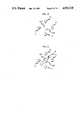
- FIG. 1is a schematic diagram of a three-port optical switching arrangement in accordance with a specific embodiment of the invention
- FIG. 2is a schematic diagram of the embodiment shown in FIG. 1 with a mirror moved into the optical path;
- FIG. 3is an assembly view of a switching assembly, comprising the embodiment shown in FIGS. 1 and 2, integrated in silicon workbench technology, in accordance with another specific embodiment in the invention;
- FIG. 4is a cross section view of a portion of the embodiment shown in FIGS. 1 and 2 (with optical fibers not in place, only for the sake of clarity) in accordance with a specific embodiment of the invention;
- FIG. 5is an assembly view of a four-port optical switching assembly suitable for use in a LAN, in accordance with another specific embodiment of the invention.
- FIG. 6is a top view of the embodiment shown in FIG. 6 with the mirror out of the optical path;
- FIG. 7is a top view of the embodiment shown in FIG. 6 with the mirror in the optical path;
- FIG. 8is a diagram of a LAN in accordance with another embodiment of the invention.
- FIG. 9is a diagram of a typical local station which is off-line in the LAN shown in FIG. 8;
- FIG. 10is a diagram of a typical local station which is on-line in the LAN shown in FIG. 8;
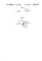
- FIG. 11is a cross-section diagram of an optical coupler in accordance with another embodiment of the invention.
- FIGS. 12-13are top views a part of a four-port optical switching assembly, in accordance with yet another specific embodiment of the invention.
- FIG. 14is a perspective view, partially in cross section, of a mirror suitable for use in a four-port optical switching assembly, in accordance with still another specific embodiment.
- FIGS. 15-16are top views of a four-port optical switching assembly, in accordance with yet another specific embodiment of the invention.
- FIGS. 17-18are top views of part of a three-port optical switching assembly, in accordance with still another specific embodiment of the invention.
- FIGS. 19-20are top views of part of a four-port optical switching assembly, in accordance with still another specific embodiment of the invention.
- a three-port (one input, two output) optical switching arrangement 10(FIG. 1) or 20 (FIG. 2) has a mirror M which is positioned either out of the optical path (FIG. 1) or in the optical path (FIG. 2).
- the switching arrangement 10, 20has first, second and third optical ports P1, P2, and P3, which are formed by respective proximate ends of first, second, and third optical fiber segments F1, F2, and F3.
- the switching arrangement 10, 20further comprises first, second and third lenslets L1, L2, and L3 which serve to collimate the respective optical beams emanating from the first fiber F1, entering into the second fiber F2 (FIG. 1), or entering into the third fiber F3 (FIG.
- Optical radiation for the optical beamsis supplied by a light source L and is collected by utilization means U1 (FIG. 1) or U2 (FIG. 2).
- the mirror M(FIG. 2) has a frontal planar reflecting surface MSI and may also have another reflecting surface parallel thereto, such as rear planar reflecting surface MS2.
- the switching arrangement 10, 20can advantageously be integrated in a silicon workbench technology assembly, to form an optical switching assembly 30 (FIG. 3).
- FIGS. 1 and 2the same reference labels are used as were used in FIGS. 1 and 2 to refer to the same or similar elements or piece-parts.
- a major planar surface PS of a silicon substrate Sfor alignment purposes there is a plurality of recesses (indentations or grooves) that are cut into the substrate S, including a mirror recess MR into which fits the mirror M.
- Other recesses cut into the substrate Sinclude: first, second, and third fiber recesses FR1, FR2, FR3; first, second, and third lenslet recesses LR1, LR2, and LR3; and first and second substrate ball recesses SBR1 and SBR2 for receiving and holding in place a pair of identical ball-bearings B1 and B2.
- the mirror Mis integral with a silicon header (holder) H.
- This headerhas a pair of mirror ball-bearing recesses MBR1 and MBR2 that are registerable with a pair of identical substrate ball-bearing recesses SBR1 and SBR2 for receiving and holding in place the ball-bearings B1 and B2.
- the mirror recess MRis made sufficiently wide to prevent the reflecting surface(s) of the mirror from touching the sides of this mirror recess MR especially when the mirror moves in and out of this recess.
- the mirror recess MR and the ball-bearing recesses SBR1, SBR2, MBR1, and MBR2are all mutually located for desired mutual alignment of the mirror surface MS1, the lenslets L1, L2, and L3, and the fiber segments F1, F2, and F3.
- FIG. 4is a cross section view of the portion the header H and substrate S indicated by the line 4-4 in FIG. 3.
- the front header surface cross section FHSis typically a ⁇ 110> plane of a mono-crystalline silicon body of which the header H is composed, and the mirror M is an integral part of the same silicon body, as formed by known lithographic masking and anisotropic etching techniques.
- the front substrate surface FSS cross section of the substrate Sis typically a ⁇ 100> plane of a monocrystalline silicon body of which the substrate S is composed.
- the header Hcan move in a rotary motion about the axis formed by joining the centers of the ball-bearings B1 and B2.
- the planar surface MS1 (and MS2) of the mirror Mis constrained to move parallel to itself, i.e., with no lateral displacement.
- the right-hand edge of the mirror M(FIGS. 3 and 4) can move smoothly into an out of the mirror recess MR, depending upon a suitable force G (or distribution of forces) applied at a point (or region) at the top of the header H located to the left of the aforementioned axis through the ball-bearings B1 and B2.
- This force Gis applied in accordance with a function of time that is suitable for the desired switching.
- the force Ggives rise to a counterclockwise torque when G is directed downward as shown in FIG. 4, and hence tends to move the relevant part of the mirror M (where the light beam is incident) out of the optical path in the switching arrangement 10, 20; and this force G gives rise to a clockwise torque when G is directed upward (not shown), and hence tends to move the mirror M into the optical path.
- the direction of Gdetermines the movement of the mirror M to produce the condition of the switching arrangement 10 vs. 20 (FIG. 1 vs. FIG. 2).
- jittering (random) motion of the mirror M upward or downwarddoes not impair optical alignment, because the alignment is completely determined by the identical ball-bearings B1 and B2 fitting into the identical recesses SBR1 and SBR2 which are located and aligned such that the mirror is constrained to move in a direction perpendicular to the place defined by the fibers F1, F2, and F3.
- mechanical vibrations which tend to produce relative motion between the substrate and the mirrordo not adversely affect the optical transmission, because the otherwise adverse transverse relative motion is suppressed by the rigidity of ball-bearings B1 and B2 in the recesses SBR1 and SBR2.
- the ball bearings B1 and B2are conveniently made of the same material as are the lenslets.
- FIG. 5shows an assembly view of a four-port (two input, two output) optical switching assembly 50 suitable for use in a LAN.
- the assembly 50can be viewed as being derived from the previously described optical switching assembly 30 by the addition of a fourth port formed by fiber segment F4 fitting into fiber recess FR4, together with lenslet L4 fitting into lenslet recess LR4, plus a second mirror surface MS2 of the mirror M parallel to the first surface MS1.
- FIG. 6shows a top view of the assembly 50 when the mirror M is out of the optical path (off-line, by-pass mode).
- optical radiation exiting from the first fiber segment F1then passes the switching arrangement 60 into the second fiber F2.
- an optical beam propagating in the fourth fiber segment F4 from another light sourcepasses into the fiber segment F3 but with an attenuated optical intensity (indicated by a dotted line), owing to a deliberately selected offset distance d of fiber segment F3 relative to fiber segment F4 (together with the same offset in their respective lenslets L3 and L4).
- the thus attenuated beam entering into the fiber segment F3,is useful for self-testing operations as more fully described below.
- An absorber Acan be added, if need be, to absorb the (excess) light coming from the fiber segment F4, i.e., to absorb the light which does not enter into the fiber segment F3.
- FIG. 7shows a top view of the switching assembly 50 (FIG. 5) when the mirror is in the path of the optical beam (active mode).
- the optical beam exiting from the fiber segment F1is passed into the switching arrangement 70 where it is reflected by the first surface MS1 of the mirror M and directed into the third fiber segment F3.
- light exiting from the fiber segment F4is reflected by the second surface MS2 of the mirror M and enters into the fiber segment F2.
- FIG. 8shows a LAN loop 800 composed of a plurality of similar local stations exemplified by a typical local station composed of node 80 together with the four-port optical switching assembly 50 described above. For example, there are a total of six such local stations interconnected by six fiber segments. One of the stations may typically function as a main station, but in any event it operates in similar manner as the others insofar as relevant here.
- FIG. 9shows a typical local station which is in the off-line condition (by-pass mode).
- a transmitter Txsuch as a light emitting diode (LED)
- a utilization meanssuch as a PIN photodiode receiver Rx
- optical radiation propagating through fiber segment F1passes through the switch 50 undisturbed and enters into the fiber segment F2.
- the beam thus propagating from F1 to F2goes on to the next local station, whereas the beam propagating from F4 to F3 can be used for testing the photo-electronics of the node 80.
- the situation of the node 80 in FIG. 9is the off-line (by-pass) mode.
- FIG. 10shows the typical local station in its on-line condition (active mode), i.e., with the mirror in the optical path.
- active modei.e., with the mirror in the optical path.
- the optical beam emanating from fiber segment F1enters into the receiver Rx, whereas the optical beam emanating from the transmitter Tx enters into the fiber segment F2.
- the situation depicted in FIG. 10is the on-line mode of the node 80, wherein the electronics of the node 80 utilizes and processes the information on the beam emanating from the fiber segment F1, and in response thereto the node 80 then transmits its own processed information to the fiber segment F4.
- FIG. 11is a design of an optical coupling arrangement, for coupling together a pair of fiber segments, such as F1 and F2, to their respective lenslets L1 and L2 in the above-described switching arrangements.
- a transparent medium R1such as silicone rubber, having a refractive index which is approximately equal to that of the segment F1, typically about 1.5.
- R1transparent medium
- the more desirable collimated beam opticsparallel beam between L1 and L2
- converging beam opticsrays coming to a focus between L1 and L2
- the space between L2 and F2is filled with a similar transparent medium R2.
- the offset distance darises in the switching assembly 60 because of the non-vanishing thickness of the mirror M.
- This offsetcauses optical loss into the absorber A, which can be undesirable in cases where the redirection of optical intensity, as is desired in self-testing, is not desired.
- the optics of the assemblycan be modified, for example, as shown in FIGS. 12-13 or 14 or 15-16 or 17-18 or 19-20.
- the same reference labelsare used to denote elements that are similar to those described above.
- all the lensletsare set in respective recesses in the substrate S (FIG. 5) as are the associated fibers, the recesses being located at respective positions that are determined by silicon workbench technology.
- FIGS. 12-13depict the lenslets L1, L2, L3, and L4 in a configuration for use in a switching assembly of the kind described above (FIG. 5).
- the remainder of the assemblyshould be understood to be the same as the switching assembly 50 shown in FIG. 5.
- a pair of auxiliary mirrors AM1 and AM2are fixedly attached either to the substrate S (FIG. 5) or to the header H and are oriented parallel to the mirror M, whereby the optical path between the fibers F4 and F3 does not suffer from any offset, as is desired.
- FIG. 14depicts a mirror 140 which, when used as the mirror M attached to the header H in the switching assembly 50 (FIG. 5), likewise avoids the offset.
- the mirror 140includes a silicon parallel slab 144 having its front surface MS1 coated with a thin layer 141 made of suitable transparent material, typically silicon dioxide, having a thickness such that it acts as an anti-reflection coating.
- the bottom half of the rear surface MS2 of the slab 144is likewise coated with a similarly thin layer 142 of the transparent material, whereas the top half of the rear surface MS2 is coated with a thin reflecting layer 143, made of suitable optically reflecting material, such as a metal having a thickness of about 100 nm.
- This mirror 140can then be used in the switching assembly 50 in the following manner.
- the mirror 140is moved upward into a position such that the optical paths among the lenslets pass through bottom (transparent) half of the mirror 140. In this way, the dielectric portion of merely the mirror deflects (refracts) the beam slightly and directs the beam along the appropriate optical path.
- the mirror 140is moved downward such that the optical paths pass through the top (reflecting) half of the mirror 140--while the bottom half of the mirror is situated in the mirror recess MR (FIG. 5). In this way the mirror 140 reflects the optical beams incident upon the front and rear surfaces of the reflecting layer 142, which has negligible thickness and hence introduces negligible offset.
- FIGS. 15-16depict an arrangement of lenslets and fibers to avoid the offset, in accordance with yet another embodiment.
- the fibers F1, F2, F3, and F4serve the same respective functions as in FIGS. 6-7, but they are all located on the same (front) side of mirror M.
- auxiliary fibers AF1, AF2, and AF3--together with auxiliary lenslets AL1, AL2, and AL3--are locatedFIG. 16) in respective alignment with these fibers F1, F2, and F3. Note that only three main lenslets L1, L2, and L3 are required, the lenslet L1 doing double duty by passing two mutually orthogonal beams simultaneously.
- the auxiliary fiber AF1is connected at its rear end by a connecting fiber CF1 to the rear end of the auxiliary fiber AF3, and the auxiliary fiber AF2 is connected at its rear end by a connecting fiber CF4 to the rear end of the auxiliary fiber AF4.
- the by-pass (off-line) modeis obtained.
- light exiting from F1goes to F2 by way of path through L1, reflection by mirror M, and through L2; and light exiting from F4 goes to F3 by way of a path through L1, reflection by mirror M, and through L3.
- the active (on-line) modeis achieved. That is, light exiting from F1 goes to F3 via L1, AL1, AF1, CF1, AF3, AL2, and L3; and light exiting from F4 goes to F2 via L1, AL4, AF4, CF2, AF2, AL2, and L2.
- FIGS. 15-16again are determined by recesses in the substrate S (FIG. 5), advantageously in accordance with silicon workbench technology, and that the position of the mirror M in FIGS. 15-16 is determined by ball-bearings (not shown in FIGS. 15-16) located in recesses, i.e., in the same way as the position of the mirror M in FIG. 5.
- FIGS. 15-16the positions of the fibers F2 and F3 can be interchanged, and at the same time the respective lenslets L2 and L3 are interchanged.
- the active (on-line) modeis obtained in the configuration shown in FIG. 15, whereas the by-pass (off-line) mode is obtained in the configuration shown in FIG. 16.
- an optically refracting elementcan be used, for example, in the form of a parallel refracting slab (plate) RS, i.e., a parallel plate composed of an optically refracting medium--as illustrated, for example, in the three-port configuration shown in FIGS. 17-18 (fibers F1, F2, F3 not shown) and in the four-port configuration shown in FIGS. 19-20 (fibers F1, F2, F3, F4 not shown). It should be understood here that optical fibers (not shown in FIGS. 17-18 or FIGS. 19-20) should be aligned as shown in FIGS. 3 and 5. In particular (FIGS.
- refracting slab RSis designed--for example, as to thickness and refractive index--such that, when it is moved into the optical path as constrained by ball-bearings B1 and B2 in their respective recesses (FIG. 4), it refracts the optical beam by an amount sufficient to deliver the beam to a different lenslet--e.g., to the lenslet L3 (FIG. 18) instead of L2 (FIG. 17).
- the front and rear planar surfaces of the refracting slab RSare both constrained to move parallel to themselves, respectively.
- AL1 and AL2are auxiliary lenslets connected by a connecting fiber CF, whereby the arrangement (FIGS. 19-20) can be used in a four-port optical switching assembly similar to the one depicted in FIG. 6-7.
- the position and orientation of the mirror M or 140 (FIG. 14), or of the parallel refracting slab RS (FIG. 18),is determined by the positions of ball-bearings B1 and B2 which fit into the recesses SBR1 and SBR2. These positions of these ball-bearings in these recesses reliably determine an axis around which the mirror M rotates in response to the applied force(s) G indicated in FIG. 4.
- the silicon workbench technologyin which the recesses for the mirror, ball-bearings, fibers, and lenslets are all simultaneously formed by reliable lithography, ensures precise relative alignment of all fibers, lenslets, and the mirror on a mass productive basis--i.e., the simultaneous manufacture of a plurality of substrates with all their recesses aligned by means of conventional lithographic techniques.
- the position and orientation of the refracting slab RS(FIGS. 18 and 20) is similarly determined by ball bearings (not shown) which fit into recesses in the substrate S as depicted in FIGS. 3-5, for example.
- the lensletscan be omitted by making the edges of the fiber segments spherical, rather than flat, to collimate the exiting optical beam.
- a single mirror M or refracting slab RScan simultaneously be used in conjuction with more than the single set of three (or four) ports--i.e., with an array of fibers containing a plurality of sets of such fibers, each set comprising three (or four) fibers operating similarly to F1, F2, F3 (and F4).
- the (center of the) mirrorcould be offset, in order to reduce the amount of optical radiation entering into the fiber segment F3 from the fiber segment F4 during the off-line mode.
- the header Hcan be a stamped metal or molded plastic body having projections that fit into recesses in the silicon substrate, while the ball-bearings are omitted.
- optical signalsinstead of optical signals, other forms of electromagnetic radiation signals can be used, spanning from optical to millimeter waves with appropriate changes in the materials of the lenslets, mirror, and waveguides.
Landscapes
- Physics & Mathematics (AREA)
- General Physics & Mathematics (AREA)
- Optics & Photonics (AREA)
- Mechanical Light Control Or Optical Switches (AREA)
- Optical Couplings Of Light Guides (AREA)
- Optical Communication System (AREA)
- Variable-Direction Aerials And Aerial Arrays (AREA)
Abstract
Description
Claims (19)
Priority Applications (6)
| Application Number | Priority Date | Filing Date | Title |
|---|---|---|---|
| US07/385,331US4932745A (en) | 1989-07-25 | 1989-07-25 | Radiation switching arrangement with moving deflecting element |
| CA002020219ACA2020219C (en) | 1989-07-25 | 1990-06-29 | Radiation switching arrangement with moving deflecting element |
| EP90307774AEP0410619B1 (en) | 1989-07-25 | 1990-07-17 | Radiation switching arrangement with moving deflecting element |
| DE69026876TDE69026876T2 (en) | 1989-07-25 | 1990-07-17 | Beam switching arrangement with movable deflection component |
| JP2190940AJP2594377B2 (en) | 1989-07-25 | 1990-07-20 | Electromagnetic radiation switching device and communication system using the same |
| HK179696AHK179696A (en) | 1989-07-25 | 1996-09-26 | Radiation switching arrangement with moving deflecting element |
Applications Claiming Priority (1)
| Application Number | Priority Date | Filing Date | Title |
|---|---|---|---|
| US07/385,331US4932745A (en) | 1989-07-25 | 1989-07-25 | Radiation switching arrangement with moving deflecting element |
Publications (1)
| Publication Number | Publication Date |
|---|---|
| US4932745Atrue US4932745A (en) | 1990-06-12 |
Family
ID=23520973
Family Applications (1)
| Application Number | Title | Priority Date | Filing Date |
|---|---|---|---|
| US07/385,331Expired - LifetimeUS4932745A (en) | 1989-07-25 | 1989-07-25 | Radiation switching arrangement with moving deflecting element |
Country Status (6)
| Country | Link |
|---|---|
| US (1) | US4932745A (en) |
| EP (1) | EP0410619B1 (en) |
| JP (1) | JP2594377B2 (en) |
| CA (1) | CA2020219C (en) |
| DE (1) | DE69026876T2 (en) |
| HK (1) | HK179696A (en) |
Cited By (55)
| Publication number | Priority date | Publication date | Assignee | Title |
|---|---|---|---|---|
| US5042889A (en)* | 1990-04-09 | 1991-08-27 | At&T Bell Laboratories | Magnetic activation mechanism for an optical switch |
| EP0490304A1 (en)* | 1990-12-14 | 1992-06-17 | ANT Nachrichtentechnik GmbH | Optical commutator |
| EP0510628A1 (en)* | 1991-04-26 | 1992-10-28 | Texas Instruments Incorporated | Optical crossbar switch |
| US5181263A (en)* | 1990-05-21 | 1993-01-19 | Motorola, Inc. | Wave-guide I/O for optical or electro-optical components |
| US5317198A (en)* | 1990-06-26 | 1994-05-31 | The Mitre Corporation | Optically controlled remote by-pass switch |
| US5345521A (en)* | 1993-07-12 | 1994-09-06 | Texas Instrument Incorporated | Architecture for optical switch |
| US5361315A (en)* | 1993-03-31 | 1994-11-01 | The Whitaker Corporation | Refractive element optical transmission switch |
| EP0826992A3 (en)* | 1996-08-28 | 1998-04-01 | Hewlett-Packard Company | Mounting a planar optical component on a mounting member |
| WO1998045740A1 (en)* | 1997-04-08 | 1998-10-15 | Paul Scherrer Institut | Device for connecting optical elements and method for producing the same |
| US5940552A (en)* | 1997-10-14 | 1999-08-17 | The Whitaker Corporation | Optical switch with multiple refractive elements pivoted into respective binary states |
| US6086776A (en)* | 1996-08-12 | 2000-07-11 | Maynard; Ronald S. | Hybrid optical multi-axis beam steering apparatus |
| US6097858A (en)* | 1998-06-05 | 2000-08-01 | Astarte Fiber Networks, Inc. | Sensing configuration for fiber optic switch control system |
| US6097860A (en)* | 1998-06-05 | 2000-08-01 | Astarte Fiber Networks, Inc. | Compact optical matrix switch with fixed location fibers |
| US6101299A (en)* | 1998-06-05 | 2000-08-08 | Astarte Fiber Networks, Inc. | Optical switch targeting system |
| US6108466A (en)* | 1998-09-17 | 2000-08-22 | Lucent Technologies | Micro-machined optical switch with tapered ends |
| US6320993B1 (en) | 1998-06-05 | 2001-11-20 | Astarte Fiber Networks, Inc. | Optical switch pathway configuration using control signals |
| US20020025104A1 (en)* | 2000-05-02 | 2002-02-28 | Steinberg Dan A. | Optical waveguide switch |
| US20020025107A1 (en)* | 2000-08-28 | 2002-02-28 | Noel Heiks | Optical switch assembly and method for making |
| US20020028037A1 (en)* | 2000-05-19 | 2002-03-07 | Steinberg Dan A. | Optical waveguide devices and methods of fabricating the same |
| US6389189B1 (en) | 1998-10-23 | 2002-05-14 | Corning Incorporated | Fluid-encapsulated MEMS optical switch |
| US6404942B1 (en) | 1998-10-23 | 2002-06-11 | Corning Incorporated | Fluid-encapsulated MEMS optical switch |
| US6445841B1 (en) | 1999-05-28 | 2002-09-03 | Omm, Inc. | Optomechanical matrix switches including collimator arrays |
| US6445840B1 (en) | 1999-05-28 | 2002-09-03 | Omm, Inc. | Micromachined optical switching devices |
| US6449407B1 (en) | 2000-03-03 | 2002-09-10 | Orix Microsystems, Inc. | Optical switch having equalized beam spreading in all connections |
| US6449406B1 (en) | 1999-05-28 | 2002-09-10 | Omm, Inc. | Micromachined optomechanical switching devices |
| US6453083B1 (en) | 1999-05-28 | 2002-09-17 | Anis Husain | Micromachined optomechanical switching cell with parallel plate actuator and on-chip power monitoring |
| US6456751B1 (en) | 2000-04-13 | 2002-09-24 | Calient Networks, Inc. | Feedback stabilization of a loss optimized switch |
| US6466711B1 (en) | 1998-06-05 | 2002-10-15 | Afn, Llc | Planar array optical switch and method |
| US20020172465A1 (en)* | 2001-05-18 | 2002-11-21 | Riza Nabeel Agha | Fault-tolerant fiber-optical multiwavelength processor |
| US20020181854A1 (en)* | 2000-04-13 | 2002-12-05 | Steinberg Dan A. | Fiber array switch having micromachined front face with roller balls |
| US6498870B1 (en) | 1998-04-20 | 2002-12-24 | Omm, Inc. | Micromachined optomechanical switches |
| US6542656B1 (en)* | 2000-04-05 | 2003-04-01 | Jds Uniphase Corporation | Add-drop optical switches including parallel fixed and movable reflectors and methods of fabricating same |
| US6546162B1 (en)* | 1999-06-17 | 2003-04-08 | Jds Fitel Inc. | 1½×2 optical switch with a transmissive switching element |
| US6544863B1 (en) | 2001-08-21 | 2003-04-08 | Calient Networks, Inc. | Method of fabricating semiconductor wafers having multiple height subsurface layers |
| US6563106B1 (en) | 2000-02-01 | 2003-05-13 | Calient Networks, Inc. | Micro-electro-mechanical-system (MEMS) mirror device and methods for fabricating the same |
| US6567574B1 (en) | 2000-10-06 | 2003-05-20 | Omm, Inc. | Modular three-dimensional optical switch |
| US20030108272A1 (en)* | 2000-12-20 | 2003-06-12 | Sherrer David W. | Optical switch assembly with flex plate and method for making |
| US6591027B2 (en) | 2001-02-27 | 2003-07-08 | Litton Systems, Inc. | Bi-stable micro-actuator and optical switch |
| US20030194172A1 (en)* | 2002-04-11 | 2003-10-16 | Memscap | Optical switching matrix and method of fabricating such a matrix |
| US6643426B1 (en) | 1999-10-19 | 2003-11-04 | Corning Incorporated | Mechanically assisted release for MEMS optical switch |
| US6665461B1 (en) | 2001-04-05 | 2003-12-16 | Richard H. Laughlin | Total internal reflection optical switch and method of operating the same |
| US6672732B1 (en)* | 1999-08-28 | 2004-01-06 | Robert Bosch Gmbh | Micromechanical oscillating device |
| US6747793B1 (en)* | 1999-11-15 | 2004-06-08 | Axsun Technologies, Inc. | System with integrated semiconductor optical amplifier array and switching matrix |
| US6751369B1 (en) | 2000-07-28 | 2004-06-15 | Moog Components Group Inc. | Fiber lens assembly for singlemode optical switches |
| US6749346B1 (en)* | 1995-11-07 | 2004-06-15 | The Board Of Trustees Of The Leland Stanford Junior University | Miniature scanning confocal microscope |
| US6771859B2 (en)* | 2001-07-24 | 2004-08-03 | 3M Innovative Properties Company | Self-aligning optical micro-mechanical device package |
| US6788840B2 (en) | 2001-02-27 | 2004-09-07 | Northrop Grumman Corporation | Bi-stable micro-actuator and optical switch |
| US6798954B2 (en)* | 2001-07-24 | 2004-09-28 | 3M Innovative Properties Company | Packaged optical micro-mechanical device |
| US6798933B2 (en)* | 2000-04-14 | 2004-09-28 | Shipley Company, L.L.C. | Fiber optic array switch |
| US6826324B2 (en)* | 2000-04-13 | 2004-11-30 | Shipley Company, L.L.C. | Optical waveguide switch |
| US6825967B1 (en) | 2000-09-29 | 2004-11-30 | Calient Networks, Inc. | Shaped electrodes for micro-electro-mechanical-system (MEMS) devices to improve actuator performance and methods for fabricating the same |
| US20040240794A1 (en)* | 2001-11-08 | 2004-12-02 | Heiks Noel A | Optical fiber right angle transition |
| US6834154B2 (en) | 2001-07-24 | 2004-12-21 | 3M Innovative Properties Co. | Tooling fixture for packaged optical micro-mechanical devices |
| US6842552B1 (en) | 2000-04-13 | 2005-01-11 | Shipley Company, L.L.C. | Optical waveguide switch |
| US6870981B2 (en) | 2000-08-24 | 2005-03-22 | Shipley Company, L.L.C. | Optical switch and method for making |
Families Citing this family (5)
| Publication number | Priority date | Publication date | Assignee | Title |
|---|---|---|---|---|
| US5178723A (en)* | 1991-11-04 | 1993-01-12 | At&T Bell Laboratories | Method and apparatus for making optical devices |
| FR2805092A1 (en)* | 2000-02-10 | 2001-08-17 | Corning Inc | LASER SOURCE THAT CAN BE SELECTED BY MEMS |
| US6445842B1 (en)* | 2000-04-05 | 2002-09-03 | Jds Uniphase, Inc. | Microelectromechanical optical cross-connect switches including mechanical actuators and methods of operating same |
| US6768830B1 (en)* | 2000-06-09 | 2004-07-27 | Agilent Technologies, Inc. | Optical add/drop switch utilizing a minimal number of switching crosspoints |
| US6526197B2 (en)* | 2001-04-09 | 2003-02-25 | Adc Telecommunications, Inc. | MEMS optical balanced path switch |
Citations (6)
| Publication number | Priority date | Publication date | Assignee | Title |
|---|---|---|---|---|
| US3870396A (en)* | 1973-07-05 | 1975-03-11 | Corning Glass Works | Optical coupler |
| US3874779A (en)* | 1973-07-05 | 1975-04-01 | Corning Glass Works | Variable ratio light coupler |
| US4239331A (en)* | 1977-12-15 | 1980-12-16 | Nippon Electric Co., Ltd. | Mechanical optical switching device |
| US4497536A (en)* | 1979-07-09 | 1985-02-05 | Post Office | Coupling of dielectric optical waveguides |
| US4580873A (en)* | 1983-12-30 | 1986-04-08 | At&T Bell Laboratories | Optical matrix switch |
| US4789228A (en)* | 1983-10-21 | 1988-12-06 | Thomson-Csf | Electrically controlled optical switching device |
Family Cites Families (4)
| Publication number | Priority date | Publication date | Assignee | Title |
|---|---|---|---|---|
| JPS55130505A (en)* | 1979-03-30 | 1980-10-09 | Ryohei Itaya | Photoswitch |
| JPS5618902U (en)* | 1979-07-19 | 1981-02-19 | ||
| CA1193477A (en)* | 1981-02-24 | 1985-09-17 | Tetsuya Yamasaki | Fixing substrate for optical fibers |
| FR2588386B1 (en)* | 1985-10-04 | 1989-02-03 | Socapex | OPTICAL SWITCH WITH ELECTROMAGNETIC CONTROL |
- 1989
- 1989-07-25USUS07/385,331patent/US4932745A/ennot_activeExpired - Lifetime
- 1990
- 1990-06-29CACA002020219Apatent/CA2020219C/ennot_activeExpired - Lifetime
- 1990-07-17EPEP90307774Apatent/EP0410619B1/ennot_activeExpired - Lifetime
- 1990-07-17DEDE69026876Tpatent/DE69026876T2/ennot_activeExpired - Lifetime
- 1990-07-20JPJP2190940Apatent/JP2594377B2/ennot_activeExpired - Lifetime
- 1996
- 1996-09-26HKHK179696Apatent/HK179696A/ennot_activeIP Right Cessation
Patent Citations (6)
| Publication number | Priority date | Publication date | Assignee | Title |
|---|---|---|---|---|
| US3870396A (en)* | 1973-07-05 | 1975-03-11 | Corning Glass Works | Optical coupler |
| US3874779A (en)* | 1973-07-05 | 1975-04-01 | Corning Glass Works | Variable ratio light coupler |
| US4239331A (en)* | 1977-12-15 | 1980-12-16 | Nippon Electric Co., Ltd. | Mechanical optical switching device |
| US4497536A (en)* | 1979-07-09 | 1985-02-05 | Post Office | Coupling of dielectric optical waveguides |
| US4789228A (en)* | 1983-10-21 | 1988-12-06 | Thomson-Csf | Electrically controlled optical switching device |
| US4580873A (en)* | 1983-12-30 | 1986-04-08 | At&T Bell Laboratories | Optical matrix switch |
Non-Patent Citations (4)
| Title |
|---|
| Electro Optic Products Siecor Corporation, Application Note 102, Moving Fiber Switches Permit Greater System Predictability and Reliability, 7 pages, no date.* |
| Electro-Optic Products-Siecor Corporation, Application Note 102, "Moving Fiber" Switches Permit Greater System Predictability and Reliability, 7 pages, no date. |
| Optics Letters, vol. 4, No. 1, Jan. 1979, "Optical Switch For Multimode Optical-Fiber Systems", by Masahiro Nunoshita, Yoshinori Nomura, Teruhito Matsui and Takashi Nakayama, pp. 27-28. |
| Optics Letters, vol. 4, No. 1, Jan. 1979, Optical Switch For Multimode Optical Fiber Systems , by Masahiro Nunoshita, Yoshinori Nomura, Teruhito Matsui and Takashi Nakayama, pp. 27 28.* |
Cited By (76)
| Publication number | Priority date | Publication date | Assignee | Title |
|---|---|---|---|---|
| US5042889A (en)* | 1990-04-09 | 1991-08-27 | At&T Bell Laboratories | Magnetic activation mechanism for an optical switch |
| US5181263A (en)* | 1990-05-21 | 1993-01-19 | Motorola, Inc. | Wave-guide I/O for optical or electro-optical components |
| US5317198A (en)* | 1990-06-26 | 1994-05-31 | The Mitre Corporation | Optically controlled remote by-pass switch |
| EP0490304A1 (en)* | 1990-12-14 | 1992-06-17 | ANT Nachrichtentechnik GmbH | Optical commutator |
| EP0510628A1 (en)* | 1991-04-26 | 1992-10-28 | Texas Instruments Incorporated | Optical crossbar switch |
| US5361315A (en)* | 1993-03-31 | 1994-11-01 | The Whitaker Corporation | Refractive element optical transmission switch |
| US5345521A (en)* | 1993-07-12 | 1994-09-06 | Texas Instrument Incorporated | Architecture for optical switch |
| US6749346B1 (en)* | 1995-11-07 | 2004-06-15 | The Board Of Trustees Of The Leland Stanford Junior University | Miniature scanning confocal microscope |
| US6137926A (en)* | 1996-08-12 | 2000-10-24 | Maynard; Ronald S. | Hybrid optical multi-axis beam steering apparatus |
| US6086776A (en)* | 1996-08-12 | 2000-07-11 | Maynard; Ronald S. | Hybrid optical multi-axis beam steering apparatus |
| EP0826992A3 (en)* | 1996-08-28 | 1998-04-01 | Hewlett-Packard Company | Mounting a planar optical component on a mounting member |
| US5862283A (en)* | 1996-08-28 | 1999-01-19 | Hewlett-Packard Company | Mounting a planar optical component on a mounting member |
| WO1998045740A1 (en)* | 1997-04-08 | 1998-10-15 | Paul Scherrer Institut | Device for connecting optical elements and method for producing the same |
| US5940552A (en)* | 1997-10-14 | 1999-08-17 | The Whitaker Corporation | Optical switch with multiple refractive elements pivoted into respective binary states |
| US6526198B1 (en) | 1998-04-20 | 2003-02-25 | Omm, Inc. | Micromachined optomechanical switches |
| US6498870B1 (en) | 1998-04-20 | 2002-12-24 | Omm, Inc. | Micromachined optomechanical switches |
| US6466711B1 (en) | 1998-06-05 | 2002-10-15 | Afn, Llc | Planar array optical switch and method |
| US6101299A (en)* | 1998-06-05 | 2000-08-08 | Astarte Fiber Networks, Inc. | Optical switch targeting system |
| US6320993B1 (en) | 1998-06-05 | 2001-11-20 | Astarte Fiber Networks, Inc. | Optical switch pathway configuration using control signals |
| US6097858A (en)* | 1998-06-05 | 2000-08-01 | Astarte Fiber Networks, Inc. | Sensing configuration for fiber optic switch control system |
| US7483602B2 (en) | 1998-06-05 | 2009-01-27 | Afn, Llc | Planar array optical switch and method |
| US20070053630A1 (en)* | 1998-06-05 | 2007-03-08 | Herzel Laor | Planar array optical switch and method |
| US6754409B2 (en) | 1998-06-05 | 2004-06-22 | Afn, Llc | Planar array optical switch and method |
| US6097860A (en)* | 1998-06-05 | 2000-08-01 | Astarte Fiber Networks, Inc. | Compact optical matrix switch with fixed location fibers |
| US6108466A (en)* | 1998-09-17 | 2000-08-22 | Lucent Technologies | Micro-machined optical switch with tapered ends |
| US6404942B1 (en) | 1998-10-23 | 2002-06-11 | Corning Incorporated | Fluid-encapsulated MEMS optical switch |
| US6389189B1 (en) | 1998-10-23 | 2002-05-14 | Corning Incorporated | Fluid-encapsulated MEMS optical switch |
| US6445841B1 (en) | 1999-05-28 | 2002-09-03 | Omm, Inc. | Optomechanical matrix switches including collimator arrays |
| US6453083B1 (en) | 1999-05-28 | 2002-09-17 | Anis Husain | Micromachined optomechanical switching cell with parallel plate actuator and on-chip power monitoring |
| US6449406B1 (en) | 1999-05-28 | 2002-09-10 | Omm, Inc. | Micromachined optomechanical switching devices |
| US6445840B1 (en) | 1999-05-28 | 2002-09-03 | Omm, Inc. | Micromachined optical switching devices |
| US6546162B1 (en)* | 1999-06-17 | 2003-04-08 | Jds Fitel Inc. | 1½×2 optical switch with a transmissive switching element |
| US6672732B1 (en)* | 1999-08-28 | 2004-01-06 | Robert Bosch Gmbh | Micromechanical oscillating device |
| US6643426B1 (en) | 1999-10-19 | 2003-11-04 | Corning Incorporated | Mechanically assisted release for MEMS optical switch |
| US6747793B1 (en)* | 1999-11-15 | 2004-06-08 | Axsun Technologies, Inc. | System with integrated semiconductor optical amplifier array and switching matrix |
| US6563106B1 (en) | 2000-02-01 | 2003-05-13 | Calient Networks, Inc. | Micro-electro-mechanical-system (MEMS) mirror device and methods for fabricating the same |
| US6449407B1 (en) | 2000-03-03 | 2002-09-10 | Orix Microsystems, Inc. | Optical switch having equalized beam spreading in all connections |
| US6542656B1 (en)* | 2000-04-05 | 2003-04-01 | Jds Uniphase Corporation | Add-drop optical switches including parallel fixed and movable reflectors and methods of fabricating same |
| US20020181854A1 (en)* | 2000-04-13 | 2002-12-05 | Steinberg Dan A. | Fiber array switch having micromachined front face with roller balls |
| US6826324B2 (en)* | 2000-04-13 | 2004-11-30 | Shipley Company, L.L.C. | Optical waveguide switch |
| US6832016B2 (en) | 2000-04-13 | 2004-12-14 | Shipley Company, L.L.C. | Fiber array switch having micromachined front face with roller balls |
| US6842552B1 (en) | 2000-04-13 | 2005-01-11 | Shipley Company, L.L.C. | Optical waveguide switch |
| US6456751B1 (en) | 2000-04-13 | 2002-09-24 | Calient Networks, Inc. | Feedback stabilization of a loss optimized switch |
| US6728433B1 (en) | 2000-04-13 | 2004-04-27 | Calient Networks, Inc. | Feedback stabilization of a loss optimized switch |
| US6798933B2 (en)* | 2000-04-14 | 2004-09-28 | Shipley Company, L.L.C. | Fiber optic array switch |
| US20020025104A1 (en)* | 2000-05-02 | 2002-02-28 | Steinberg Dan A. | Optical waveguide switch |
| US20040228600A1 (en)* | 2000-05-19 | 2004-11-18 | Steinberg Dan A. | Optical waveguide devices and methods of fabricating the same |
| US20040208469A1 (en)* | 2000-05-19 | 2004-10-21 | Steinberg Dan A. | Optical waveguide devices and methods of fabricating the same |
| US6973253B2 (en) | 2000-05-19 | 2005-12-06 | Shipley Company, L.L.C. | Optical waveguide devices and methods of fabricating the same |
| US6748131B2 (en) | 2000-05-19 | 2004-06-08 | Shipley Company, L.L.C. | Optical waveguide devices and methods of fabricating the same |
| US20020028037A1 (en)* | 2000-05-19 | 2002-03-07 | Steinberg Dan A. | Optical waveguide devices and methods of fabricating the same |
| US20060275012A1 (en)* | 2000-05-19 | 2006-12-07 | Shipley Company, L.L.C. | Optical waveguide devices and methods of fabricating the same |
| US7065283B2 (en) | 2000-05-19 | 2006-06-20 | Shipley Company, L.L.C. | Optical waveguide devices and methods of fabricating the same |
| US6751369B1 (en) | 2000-07-28 | 2004-06-15 | Moog Components Group Inc. | Fiber lens assembly for singlemode optical switches |
| US6870981B2 (en) | 2000-08-24 | 2005-03-22 | Shipley Company, L.L.C. | Optical switch and method for making |
| US20020025107A1 (en)* | 2000-08-28 | 2002-02-28 | Noel Heiks | Optical switch assembly and method for making |
| US6853764B2 (en) | 2000-08-28 | 2005-02-08 | Shipley Company, L.L.C. | Optical switch assembly and method for making |
| US6825967B1 (en) | 2000-09-29 | 2004-11-30 | Calient Networks, Inc. | Shaped electrodes for micro-electro-mechanical-system (MEMS) devices to improve actuator performance and methods for fabricating the same |
| US6567574B1 (en) | 2000-10-06 | 2003-05-20 | Omm, Inc. | Modular three-dimensional optical switch |
| US7079725B2 (en) | 2000-12-20 | 2006-07-18 | Shipley Company, L.L.C. | Optical switch assembly with flex plate and method for making |
| US6810162B2 (en) | 2000-12-20 | 2004-10-26 | Shipley Company, L.L.C. | Optical switch assembly with flex plate and method for making |
| US20030108272A1 (en)* | 2000-12-20 | 2003-06-12 | Sherrer David W. | Optical switch assembly with flex plate and method for making |
| US20050074201A1 (en)* | 2000-12-20 | 2005-04-07 | Sherrer David W. | Optical switch assembly with flex plate and method for making |
| US6591027B2 (en) | 2001-02-27 | 2003-07-08 | Litton Systems, Inc. | Bi-stable micro-actuator and optical switch |
| US6788840B2 (en) | 2001-02-27 | 2004-09-07 | Northrop Grumman Corporation | Bi-stable micro-actuator and optical switch |
| US6665461B1 (en) | 2001-04-05 | 2003-12-16 | Richard H. Laughlin | Total internal reflection optical switch and method of operating the same |
| US20020172465A1 (en)* | 2001-05-18 | 2002-11-21 | Riza Nabeel Agha | Fault-tolerant fiber-optical multiwavelength processor |
| US6859578B2 (en) | 2001-05-18 | 2005-02-22 | Nuonics, Inc. | Fault-tolerant fiber-optical multiwavelength processor |
| US6834154B2 (en) | 2001-07-24 | 2004-12-21 | 3M Innovative Properties Co. | Tooling fixture for packaged optical micro-mechanical devices |
| US6798954B2 (en)* | 2001-07-24 | 2004-09-28 | 3M Innovative Properties Company | Packaged optical micro-mechanical device |
| US6771859B2 (en)* | 2001-07-24 | 2004-08-03 | 3M Innovative Properties Company | Self-aligning optical micro-mechanical device package |
| US6544863B1 (en) | 2001-08-21 | 2003-04-08 | Calient Networks, Inc. | Method of fabricating semiconductor wafers having multiple height subsurface layers |
| US20040240794A1 (en)* | 2001-11-08 | 2004-12-02 | Heiks Noel A | Optical fiber right angle transition |
| US7410304B2 (en) | 2001-11-08 | 2008-08-12 | Rohm And Haas Electronic Materials Llc | Optical fiber right angle transition |
| US6847756B2 (en)* | 2002-04-11 | 2005-01-25 | Memscap | Optical switching matrix and method of fabricating such a matrix |
| US20030194172A1 (en)* | 2002-04-11 | 2003-10-16 | Memscap | Optical switching matrix and method of fabricating such a matrix |
Also Published As
| Publication number | Publication date |
|---|---|
| DE69026876D1 (en) | 1996-06-13 |
| HK179696A (en) | 1996-10-04 |
| CA2020219C (en) | 1995-02-28 |
| EP0410619A3 (en) | 1992-05-13 |
| EP0410619B1 (en) | 1996-05-08 |
| DE69026876T2 (en) | 1996-12-05 |
| JP2594377B2 (en) | 1997-03-26 |
| JPH0359611A (en) | 1991-03-14 |
| CA2020219A1 (en) | 1991-01-26 |
| EP0410619A2 (en) | 1991-01-30 |
Similar Documents
| Publication | Publication Date | Title |
|---|---|---|
| US4932745A (en) | Radiation switching arrangement with moving deflecting element | |
| US5943454A (en) | Freespace optical bypass-exchange switch | |
| US6163643A (en) | Micro-mechanical variable optical attenuator | |
| US4927225A (en) | 2×2 Optical bypass switch | |
| US6618519B2 (en) | Switch and variable optical attenuator for single or arrayed optical channels | |
| US6415067B1 (en) | N x M optical switch | |
| US6081635A (en) | Microoptical module with a WDM filter and an optical isolator for fiber-optic amplifier systems | |
| US6400858B1 (en) | 1×N reflector switch | |
| CA2339397A1 (en) | Optical fiber-lens array | |
| US6591032B2 (en) | Optical switching and attenuation systems and methods therefor | |
| US6751369B1 (en) | Fiber lens assembly for singlemode optical switches | |
| CN210514694U (en) | 2 XN's MEMS photoswitch | |
| EP0965868B1 (en) | 2 x 2 optical fiber switch | |
| US4854660A (en) | Linear translation switch with optical fibers | |
| US20030138210A1 (en) | Optical fiber with collimated output having low back-reflection | |
| US6678438B2 (en) | Apparatus and method for switching an optical path | |
| US6912335B2 (en) | Optical switch with reduced beam divergence | |
| US6970615B1 (en) | Compact high-stability optical switches | |
| US7181102B1 (en) | Optical switching systems and methods | |
| US20020146199A1 (en) | Mems optical balanced path switch | |
| US6363186B1 (en) | X-cube integrated solid optics component | |
| US6591031B2 (en) | Optical switch with movable mirror | |
| EP1245976A1 (en) | Optical switch configuration | |
| US6909820B2 (en) | 2×2 fiber optic switch with reflective element | |
| JP3782318B2 (en) | Optical switching device and optical switching method |
Legal Events
| Date | Code | Title | Description |
|---|---|---|---|
| AS | Assignment | Owner name:BELL TELEPHONE LABORATORIES, INCORPORATED, 600 MOU Free format text:ASSIGNMENT OF ASSIGNORS INTEREST.;ASSIGNOR:BLONDER, GREG E.;REEL/FRAME:005104/0829 Effective date:19890725 Owner name:AMERICAN TELEPHONE AND TELEGRAPH COMPANY, 550 MADI Free format text:ASSIGNMENT OF ASSIGNORS INTEREST.;ASSIGNOR:BLONDER, GREG E.;REEL/FRAME:005104/0829 Effective date:19890725 | |
| STCF | Information on status: patent grant | Free format text:PATENTED CASE | |
| CC | Certificate of correction | ||
| FEPP | Fee payment procedure | Free format text:PAYOR NUMBER ASSIGNED (ORIGINAL EVENT CODE: ASPN); ENTITY STATUS OF PATENT OWNER: LARGE ENTITY | |
| FPAY | Fee payment | Year of fee payment:4 | |
| FEPP | Fee payment procedure | Free format text:PAYER NUMBER DE-ASSIGNED (ORIGINAL EVENT CODE: RMPN); ENTITY STATUS OF PATENT OWNER: LARGE ENTITY Free format text:PAYOR NUMBER ASSIGNED (ORIGINAL EVENT CODE: ASPN); ENTITY STATUS OF PATENT OWNER: LARGE ENTITY | |
| FEPP | Fee payment procedure | Free format text:PAYOR NUMBER ASSIGNED (ORIGINAL EVENT CODE: ASPN); ENTITY STATUS OF PATENT OWNER: LARGE ENTITY Free format text:PAYER NUMBER DE-ASSIGNED (ORIGINAL EVENT CODE: RMPN); ENTITY STATUS OF PATENT OWNER: LARGE ENTITY | |
| FPAY | Fee payment | Year of fee payment:8 | |
| FPAY | Fee payment | Year of fee payment:12 |