US4932022A - Integrated voice and data telephone system - Google Patents
Integrated voice and data telephone systemDownload PDFInfo
- Publication number
- US4932022A US4932022AUS07/326,405US32640589AUS4932022AUS 4932022 AUS4932022 AUS 4932022AUS 32640589 AUS32640589 AUS 32640589AUS 4932022 AUS4932022 AUS 4932022A
- Authority
- US
- United States
- Prior art keywords
- data
- telephone
- menu
- displaying
- softkey
- Prior art date
- Legal status (The legal status is an assumption and is not a legal conclusion. Google has not performed a legal analysis and makes no representation as to the accuracy of the status listed.)
- Expired - Lifetime
Links
- 230000006870functionEffects0.000claimsabstractdescription62
- 238000004891communicationMethods0.000claimsabstractdescription47
- 230000002452interceptive effectEffects0.000claimsabstractdescription5
- 230000005540biological transmissionEffects0.000claimsdescription13
- 238000000034methodMethods0.000description116
- 230000008569processEffects0.000description105
- 239000000872bufferSubstances0.000description24
- 238000013461designMethods0.000description23
- 238000010586diagramMethods0.000description19
- 230000011664signalingEffects0.000description18
- 230000004044responseEffects0.000description13
- 238000000354decomposition reactionMethods0.000description9
- 238000011161developmentMethods0.000description8
- 230000018109developmental processEffects0.000description8
- 238000003860storageMethods0.000description8
- 230000007704transitionEffects0.000description8
- 238000013459approachMethods0.000description7
- 230000010354integrationEffects0.000description7
- 230000008901benefitEffects0.000description6
- 230000007246mechanismEffects0.000description6
- 238000012545processingMethods0.000description6
- 238000012360testing methodMethods0.000description6
- 238000009826distributionMethods0.000description5
- 238000009434installationMethods0.000description5
- 239000000203mixtureSubstances0.000description5
- 238000007726management methodMethods0.000description4
- 238000004519manufacturing processMethods0.000description4
- 230000003068static effectEffects0.000description4
- 230000026676system processEffects0.000description4
- 230000001419dependent effectEffects0.000description3
- 239000004973liquid crystal related substanceSubstances0.000description3
- 238000012544monitoring processMethods0.000description3
- 230000001960triggered effectEffects0.000description3
- 230000002457bidirectional effectEffects0.000description2
- 230000000903blocking effectEffects0.000description2
- 230000008859changeEffects0.000description2
- 230000006378damageEffects0.000description2
- 238000005516engineering processMethods0.000description2
- 238000009499grossingMethods0.000description2
- 238000010348incorporationMethods0.000description2
- 238000012423maintenanceMethods0.000description2
- 230000001343mnemonic effectEffects0.000description2
- 238000003825pressingMethods0.000description2
- 230000033772system developmentEffects0.000description2
- 238000013519translationMethods0.000description2
- 101150108015STR6 geneProteins0.000description1
- 101100386054Saccharomyces cerevisiae (strain ATCC 204508 / S288c) CYS3 geneProteins0.000description1
- 230000009471actionEffects0.000description1
- 230000003466anti-cipated effectEffects0.000description1
- 238000003491arrayMethods0.000description1
- 230000015572biosynthetic processEffects0.000description1
- 238000004422calculation algorithmMethods0.000description1
- 239000003990capacitorSubstances0.000description1
- 230000003750conditioning effectEffects0.000description1
- 239000013078crystalSubstances0.000description1
- 230000003247decreasing effectEffects0.000description1
- 230000001934delayEffects0.000description1
- 238000012938design processMethods0.000description1
- 230000000694effectsEffects0.000description1
- 238000011156evaluationMethods0.000description1
- 238000001914filtrationMethods0.000description1
- 230000003993interactionEffects0.000description1
- 230000007774longtermEffects0.000description1
- 238000013507mappingMethods0.000description1
- 239000011159matrix materialSubstances0.000description1
- 230000003340mental effectEffects0.000description1
- 238000001465metallisationMethods0.000description1
- 230000002093peripheral effectEffects0.000description1
- 238000004886process controlMethods0.000description1
- 238000011165process developmentMethods0.000description1
- 238000011867re-evaluationMethods0.000description1
- 239000012925reference materialSubstances0.000description1
- 230000008439repair processEffects0.000description1
- 238000011160researchMethods0.000description1
- 230000004043responsivenessEffects0.000description1
- 230000000630rising effectEffects0.000description1
- 238000005070samplingMethods0.000description1
- 238000013515scriptMethods0.000description1
- 101150035983str1 geneProteins0.000description1
- 230000001360synchronised effectEffects0.000description1
- 210000003371toeAnatomy0.000description1
- 238000012546transferMethods0.000description1
- XLYOFNOQVPJJNP-UHFFFAOYSA-NwaterSubstancesOXLYOFNOQVPJJNP-UHFFFAOYSA-N0.000description1
Images


Classifications
- H—ELECTRICITY
- H04—ELECTRIC COMMUNICATION TECHNIQUE
- H04Q—SELECTING
- H04Q11/00—Selecting arrangements for multiplex systems
- H04Q11/04—Selecting arrangements for multiplex systems for time-division multiplexing
- H04Q11/0428—Integrated services digital network, i.e. systems for transmission of different types of digitised signals, e.g. speech, data, telecentral, television signals
- Y—GENERAL TAGGING OF NEW TECHNOLOGICAL DEVELOPMENTS; GENERAL TAGGING OF CROSS-SECTIONAL TECHNOLOGIES SPANNING OVER SEVERAL SECTIONS OF THE IPC; TECHNICAL SUBJECTS COVERED BY FORMER USPC CROSS-REFERENCE ART COLLECTIONS [XRACs] AND DIGESTS
- Y10—TECHNICAL SUBJECTS COVERED BY FORMER USPC
- Y10S—TECHNICAL SUBJECTS COVERED BY FORMER USPC CROSS-REFERENCE ART COLLECTIONS [XRACs] AND DIGESTS
- Y10S379/00—Telephonic communications
- Y10S379/914—Programmable telephone component
- Y10S379/915—Soft key
Definitions
- the present iventionrelates to a integrated voice and data telephone system for use in a business environment. Communications are undergoing rapid and dramatic change with the incorporation of display terminals, personal computers, and word processors.
- the computer controlled systemsrequire, in general, processing of data in digital format, as contrasted to conventional telephone systems which operate in an analog or analog-to-digital format. Consequently, one problem which has faced business communication systems is the incorporation of data and voice inforamtion into a compatible fashion.
- a more particular object of the present inventionis to provide integration of voice and data communications which employs a distributed architecture scheme.
- an object of the present inventionis to provide an improved telephone station set which provides compact and efficient interaction of voice, data and messages for a user.
- These capabilitiesinclude interactive messaging, access to personnel directories, the ability to handle both voice and data traffic simultaneously, full choice of call routing, user administration of features and the like.
- the telephone station setis connected to a pair of telephone subscriber lines for transmitting and receiving voice and data information on those subscriber lines.
- the telephone station setprovides the capability of converting analog voice information to a digital format and includes a two-line by forty character interactive liquid crystal display which guides a user with an orderly flow of information, on-call status, prompts, menus, caller identity, a speed dialing directory and messages, depending on the need at any particular moment.
- the menu driven displaysare softkey selectible so that a plurality of changeable menu functions can be displayed on an as-needed basis.
- the telephone station setis responsive to a selected one of the displayed menu functions for enabling that selected menu function, such as indicated above. Functions or commands which are invalid at the moment are not presented as a choice or selection, thus reducing the possibility of user error.
- FIG. 1depicts a block diagram of the present invention.
- FIG. 1Adepicts a block diagram of an expanded version of the present invention.
- FIG. 2depicts a perspective view of a telephone station set, which forms a part of FIG. 1.
- FIG. 3depicts a more detailed view of the telephone station set of FIG. 2, illustrating the liquid crystal display and softkeys.
- FIG. 4depicts a block diagram of a bus interface chip, which forms a portion of FIG. 1.
- FIGS. 5-7depict timing diagrams for the bus interface chip of FIG. 4.
- FIG. 8depicts a block diagram of a station link encoder-decoder which forms a portion of FIG. 1.
- FIGS. 9A-9D and 10depict timing diagrams for the station link encoder-decoder of FIG. 8.
- FIG. 11depicts a diagram illustrating the major components of the network operating system (NOS) according to the present invention.
- NOSnetwork operating system
- FIG. 12depicts the NOS name and address formats.
- FIG. 13depicts the NOS standard message format.
- FIG. 14depicts a block diagram illustrating the NOS architecture.
- FIG. 15depicts a block diagram of a universal codec board, which forms part of the present invention.
- FIG. 16depicts a fabrication outline of the UCB of FIG. 15.
- FIG. 17depicts an assembly drawing for the UCB of FIG. 16.
- FIG. 18depicts a schematic diagram of one UCB.
- FIG. 19depicts a schematic diagram of another UCB, different from that of FIG. 18.
- the design of the improved business communications systemreflects a new architectural approach that contrasts with the conventional designs of most PBXs and local area networks (LANs). Rather than relying on a central call processor to oversee or perform every operating detail in the system, the present invention incorporates a strongly hierachical approach.
- the control moduleincludes the central processor, mass storage devices, and control processor switch. It also contains 18 slots for any mix of interface units (IU's) which provide connection to the Central Office trunks, several kinds of station instruments and a variety of data devices.
- IU'sinterface units
- the basic system 10comprises a central module 12 linked over two separate high-speed buses 14, 16 to a series of specialized interface units (IU's) 20-28.
- the IUsare circuit cards that interpret and pass on command messages between the Module 12 and lower level devices and facilities, such as telephone stations sets, computers and outside trunks.
- the interface units of FIG. 1are described below.
- the Station Interface Unit (SIU) 20serves up to eight Telephone Station Sets 30. SIU 20 provides eight voice ports and, with the addition of a Data Adapter Device inside each Station Set, eight asynchronous RS-232C data ports.
- the Data Interface Unit (DIU) 22permits use of up to four stand-alone RS-232C devices (such as computer 32, a printer, a digital facsimile machine or modem) without associated voice facilities. In one embodiment, data rates up to 19.2 kilobits per second (kb/s) asynchronous are supported.
- the Central Office Interface Unit (COIU) 24serves any mix of up to four incoming, outgoing or two-way central office loop-start lines or ground-start trunks.
- Each Pair Interface Unit 26provides eight voice ports for conventional rotary-dial and pushbutton telephones, such as telephone 34, over single-pair station wire 36. This unit also provides interfaces with any or all of the many devices such as answering machines or alarm systems which connect with telephone lines.
- IUscould interface with LANs, T1 Pulse Code Modulation (PCM) trunks, video transmission facilities, Circuit, Switched Digital Circuits (CSDC), and packetswitched networks such as X.25 and others.
- PCMPulse Code Modulation
- CSDCSwitched Digital Circuits
- Module 12incorporates an 8086-based processor 40 and, in one embodiment, up to 16 megabytes (MB) of random access memory (RAM). As little as 0.5 MB of RAM is possible, but small installations typically would employ about 1 MB.
- MBmegabytes
- the Module 12also houses a 5 MB Winchester-type hard disk drive 42 for mass storage of various system data such as call processing software, diagnostics, directories, specialized applications, features, and the like (up to 300 MB of mass storage is possible in other embodiments).
- a 360 kilobyte floppy disk drive 44is provided for convenient loading of new software, such as program upgrades or new feature sets.
- the disk drivescan be purchased with more capacity in the same physical sizes and with the same electronic interfaces.
- the Module 12provides a circuit bus 16 with 256 Time Division Multiplexed (TDM) time slots with which it can provide full duplex, non-blocked service up to 120 physical ports.
- a porthere is defined as a station with the potential of both voice and data, a CO trunk or other physical wired input.
- the physical housing of the Moduole 12provides 18 card slots into which the IUs and a service unit card 28 are mounted in any combination.
- the modulewill accommodate 256 logical ports in a non-blocking mode.
- a logical portis a voice or data input from a TSS, a CO trunk, a DIU data input, a POTS phone input or a SU tone, for example.
- the service unit 28supplies digital tones and ringing signals for the local stations as well as conference and maintenance capabilities.
- the actual number of ports which can be served by a single moduledepends on the mix of IUs employed in each configuration, i.e., the mix of central office trunks, data terminals, Station Sets, modems and the like.
- Module Control Processor Switch 46provides the system for adding a redundant Module Processor in other applications.
- the internal backbone of the system 10is a very flexible circuit bus 16 with dynamically allocated bandwidth totaling 18 megabits per second (Mb/s).
- time slots on this busmay be allocated from 256 to 2000 in number.
- the minimum time slot element of 9 kb/sincludes one 8-kb/s digital channel plus one 1-kb/s in-band supervisory channel, so that a dual-dynamic bus allocation capability is provided.
- a 72-kb/s bandwidthis assigned and composed of eight of these 9-kb/s channels. Since each 9-kb channel is built up out of an 8-kb digital channel and a 1-kb supervisory channel, the North American and ISDN standards of 64 kb/s are embedded.
- the transaction bus 14 of FIG. 1transmits control messages in packet-type format between the Module 12 and the various IUs.
- Each packet message at the NOS levelis labeled with the name of its addressee, which may be located anywhere in the system 10. This tenchnique gives the system 10 immense flexibility and frees it of constraints imposed by any particular configuration.
- Typical examples of transaction messagesinclude the equivalent of: "Seize an outgoing WATS trunk and dial this telephone number. . . ,” and “Put this tone out and write this message on the display.”
- Each messageis sent in an efficient packet format including the destination name, the message or command and a checksum.
- the bandwidth of transaction bus 14is 670 kilobytes per second, which assures ample capacity for a avoiding delays in call set-up or message passing, even in very busy systems.
- each of the IUs(except the SIU 20) contain its own 8085 processor which receives and implements commands or queries from the Module processor 40 and originates messages of its own to the Module processor 40.
- the SIU 20does not require its own processor because it interfaces with up to eight Telephone Station Sets 30, each having its own 8085 processor, and in addition a second 8048 microprocessor when equipped with a Data Adapter Device. These 8085's manage the communications protocol, the display and the keyboard; the 8048 manages data transmission between the station processor and circuit bus subsystem via the SLED.
- the SIU 20serves primarily as an interface between the system buses 14, 16 and the station wiring over which it transmits and receives a continuous 256 kb/s full duplex stream up to a distance of one-half mile. This includes 72 kb/s each for data and voice, plus 16 kb/s for control, supervision and display messages.
- a gate array chip, the Station Link Encoder-Decoder (SLED)is located in each SIU 20 and Station Set 30.
- the SLED chippackages the digital voice, data and control bit stream for transmission over the station wiring at 256 kb/s.
- a second chipis resident on each IU of FIG. 1. This chip is the Bus Interface Circuit (BIC) and controls communication between the IU and the Circuit Bus 16.
- BICBus Interface Circuit
- LSIlarge scale integrated
- FIG. 1Athere is depicted therein a block diagram of a business communication system (BCS) which illustrates in more detail the functional interconnections of a control processor module (CPM).
- BCSbusiness communication system
- CCMcontrol processor module
- an interface unitconnects to the telephone station set (TSS), a pair interface unit (PIU), a data interface unit (DIU), or central office interface unit (COIU), as illustrated in FIG. 1.
- TSStelephone station set
- POUpair interface unit
- DIUdata interface unit
- COIUcentral office interface unit
- FIG. 1AThe system illustrated in block diagram form in FIG. 1A is provided as a further aid in illustrating the aspects of the present invention.
- a mnemonic tableis set forth below to provide an indication of the various acronums illustrated in FIG. 1A.
- the Telephone Station Set (TSS) 30is a simple and compact user terminal which provides many functional capabilities.
- a perspective view of an improved telephone station set 30is illustrated in FIG. 2.
- the TSS 30 in FIG. 2has relatively few keys--25--, but commands all the capabilities for which other station sets require 40 to 60 keys or even more.
- the unintimidating simplicity of the TSS 30combined with its unusual versatility and intuitive ease of use encourage its use without requiring that novice users be trained or keep reference material on hand, e.g., lists of speed dial numbers or keystroke protocols for invoking features. This aspect serves as a mental reminder of choices currently at hand.
- the displayprovides an English language display as contrasted with current codes, such as "#", "*" and the like.
- FIG. 3depicts a more detailed view of the TSS 30 of FIG. 2.
- a telephone callcould be set up as a conference call by pressing softkey 52, or in the alternative, the call could be transferred by pressing softkey 54.
- the TSS 30 of FIGS. 2 and 3incorporates a North American standard mu-law codec to digitally encode analog speech signals into standard PCM format. Up to 24 KB of memory (RAM and ROM) are included within the set for local features.
- the TSS 30may contain an optional RS-232C port which allows terminals personal computers (such as computer 36 of FIG. 1) and the like to be connected to the station and become part of the system. This capability is obtained by the addition of the Data Adapter Device (DAD), a small printed circuit board within the TSS 30.
- DADData Adapter Device
- the TSS of FIGS. 2 and 3also incorporates a speakerphone 62 and controls for adjusting the viewing angle of the LCD 50 and the volume settings of the ringer and speakerphone.
- the bus interface chipprovides an interface between two serial I/O lines and a parallel, timeslotted module bus.
- the BICis a high performance CMOS semi-custom gate array.
- the BICis utilized on all BUS IUs. It is designed to be particulary efficient interfacing to a Station Link Encoder-Decoder (SLED, to be described later), but is also useful for interfacing virtually any type of IU to the module circuit bus 16.
- SLEDStation Link Encoder-Decoder
- the functions performed by the BICcould be performed by discrete LSTTL logic.
- the advantages of using a gate array insteadare lower cost in high production volumes, less physical size, lower power, less heat, and improved reliability through decreased parts count.
- CMOS LSI deviceswith between 500 and 10,000 uncommitted gates on an unmetalized water. Customizing involves creating the metalization layer or layers in order to define the specific function of the device. For conceptual purposes, the device can be looked upon as a "board" of conventional TTL devices condensed to a single chip. The only devices which must still be provided off-chip are drivers and buffers which provide board I/Os; conventional LSTTL devices in these applications are considerably more robust against transients and static discharge.
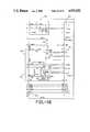
- the BIC illustrated in FIG. 4replaces most of the digital circuitry on a typical IU. It interfaces between a station link encoder-decoder on a station IU, or two codecs on a POTS/CC IU, and the module bus. Two serial input channels and two serial output channels are provided which can send or receive on any of 256 timeslots of a 10 bit wide parallel bus. A processor interface is provided to allow the module processor to control timeslot selection, commands, and status information to and from the BIC.
- two channels of serial input dataenter two serial to parallel converters 100, 102.
- Datais clocked into both inputs on the rising edge of a common data clock. Separate eneable inputs define the period of the eight valid data bits. Data may be clocked in a virtually any rate between 64 KHz and 2 MHz providing that the entire new 8 bit word is ready before frame sync.
- the ninth "signaling" bitenters separately, and is strobed into one of two latches 104, 106, simultaneously with the first bit of serial data per frame.
- a data selector 110chooses one of the two latch outputs which will apply data to the bus during the next timeslot.
- Parityis generated by parity generator 112 on the combination of the eight bit parallel data and the signaling data.
- Frame synccauses the parallel data, the signalling bit data, and the parity bit to be latched in latch 114.
- the latch outputsare connected to bidirectional output drivers 116, which place the latched data on to the output pins of the device when enabled by the control generator circuit 120 (to be described later).
- Two 10 bit latches 130, 132can sample data from the device's circuit bus pins. Again, the control circuit 120 issues enable signals during the appropriate time slots to latch the correct data.
- Parityis checked on the received data by parity check circuits 134, 136.
- a signalis sent to the status/control register 130 and the processor interface and control 140 if there is a received parity error.
- the parallel data latched during the previous frameis loaded into the parallel to serial converters 142, 144.
- the converters 142,144output two serial data channels. Signaling bits are latched at the beginning of each data enable so that new signaling information is available concurrently with the new data.
- the processorcan command the loopback circuit to attach the serial output to the serial input.
- the timeslot registersare correctly set, this causes data received on one timeslot to be placed back on another timeslot.
- the firstare independent of the timeslots which are being read or written. These are generally dependent on frame sync and are used to move data between latches and the serial-parallel interfaces.
- the secondare those which enable latches or buffers during a particular timeslot and frame.
- the specific timeslot and frameare under the control of an external processor via a set of registers which it loads with the appropriate time-slot/frame information.
- a counter 150keeps track of the current timeslot and frame, and a set of comparators checks the counter output versus each register's contents. When the current timeslot/frame matches that loaded into a register, the appropriate control signal is invoked.
- Either of the two channelscan be set up to send and receive on any timeslot pair.
- datacan be sent on any combination of frames within the superframe.
- the receiveris always enabled on all frames of the superframe for a given timeslot.
- the reset inputis a special control signal which sets the BIC to a known state. With a reset input, all error registers are cleared and the transmit submux registers are cleared so that no data will be placed on the parallel circuit bus.
- the processor interface 140allows loading of any of the timeslot/frame registers via an 8 bit processor I/O bus 160. Data formats are specified below.
- timeslot/frame registers 154When timeslot/frame registers 154 are loaded, the actual information is not transferred to the registers until a control register is loaded by processor 140. Loading will be arbitrated by processor interface control 140 relative to framesync and the bus clock to insure that the enabling or disabling of a timeslot/frame combination will not result in glitches on either the parallel or serial outputs.
- Timing requirements for input signals and timing specifications for output signals from the BIC of FIG. 4will be described in conjunction with FIGS. 5-7. Timing specifications are given in two parts: first, for those signals which interface to the circuit system, and second for those which interface to the processor system.
- This timing for the serial data inputs/outputs, signaling bit input/outputs, and enable signal inputs relative to the serial data clockare applicable to either the A or B channels.
- Table IV belowdescribed the timing signals illustrated in FIG. 5.
- the timing for the parallel module bus interface signalsincluding the driver enable outputs, referenced to the bus clock inputs, are illustrated in FIG. 6 and set forth in Table V below.
- the timing for the processor bus interface signalsis illustrated in FIG. 7 and set forth in Table VI below.
- the ter, tdv, tdz and tew signalsare taken to be from the latest of RS1, RS0 or DSL.
- the BICis controlled by the module processor. There are four ports which can be read from or written to. One port is used as a status/control port. The other three are used to write a three byte sequence to control the timeslot and sub-multiplex frame assignments.
- the status/control portis addressed when RS0 and RS1 are both logical zero. Reading the BIC status/control port returns a single byte of status and eror information decoded as follows. ##STR1##
- a processor write errorindicates that bad parity was received from the processor. Reading the port clears the error registers.
- Resetperforms the same functions as the hardware reset.
- the timeslot/submux portsare written to in a three byte sequence. They should be written in the correct sequence: first the timeslot and submux registers, then the command register. Writing the command register causes the timeslot and frame register data to be transferred to the actual timeslot/frame register pair specified in the command register.
- the command byteis written with RS1-0. It is coded as follows: ##STR3##
- a read of the timeslot or frame portsallows the register contents to be checked.
- FIG. 8a block diagram of the station link encoder-decoder (SLED) is illustrated.
- the SLEDprovides three digital communication channels between the BCS central equipment and the Telephone Station Set (SS) of FIG. 1.
- SSTelephone Station Set
- the station setis the primary user interface to the BCS of FIG. 1, interfacing with the BCS central equipment via standard office telephone wiring.
- a station linkprovides a digital communication channel between the central equipment and a station set. It is submultiplexed into three digital channels to allow the transmission of digitized voice, data, and station to central equipment control information.
- the data coding formatSince the digital channel is ultimately sent via 24 gauge twisted pair telephone grade wire, the data coding format must have sufficient robustness to avoid errors caused by noise "hits" on the line. The coding must also be able to provide sufficient clock information at the receiving end to decode the data, as there is no facility for sending separate clock.
- the Station Link Encoder-Decoderis a semi-custom CMOS integrated circuit which is installed at both ends of the station link.
- the SLEDperforms multiplexing and demultiplexing, data encoding and decoding, and a processor interface.
- Three two-way digital channelsare provided in the station link. These three channels are:
- a 72 kilobit/sec channel used for transmission of digitized voice(utilized as a 64 kb/sec voice channel and a simultaneous 8 kb/sec channel for signaling).
- a 72 kilobit/sec channel used for data transmission(utilization to be defined in the specification for the station set data interface option).
- a 16 kilobit/sec channel used for communication between the station set processor and the module processor(the "control channel").
- the SLEDis installed on both the station interface unit (SIU) and at the station set.
- SIUstation interface unit
- the SLEDperforms two basic functions:
- Each 72 kB/s channelis further broken down into a 64 kB/s and an 8 kB/s channel.
- the two 64 kB/s channelshave serial I/O interfaces.
- the inputsare separate for the two channels, and the outputs are combined on a multiplexed output line.
- the signaling channelsuse completely separate input and output lines to allow maximum flexibility when installed in station or central equipment.
- Datais then routed to the data encoder 206 through delay 204.
- the encoder 206converts the serial data into Manchester II encoded data minus the required synchronization sequences.
- the data encoder 206 outputis sent to the sync encoder 210; which applies Manchester II synchronization sequences at the beginning of each data packet under control of the sync controller.
- the sync encoder 206 outputis sent through an I/O buffer 212 and out of the device.
- Received datais sent via buffer 214 to an integrator 220, which serves to prevent noise hits from being improperly detected as data transitions.
- received datais sent to a transition detector 222 which has outputs indicating whether a high-to-low or low-to-high transition has occurred on the input.
- Transition detector 22 outputis routed to a set of latches 230, 232, which, by means of the control and timing circuits 202 latch the high-to-low transistion detector output. By selecting which transitions are latched, the data and signaling information is extracted from the transition detector output.
- the SLEDcontains a processor interface 240 which is used both for control channel information I/O and a status/control register.
- the interface controllerenables the correct buffers and latches at the appropriate times to read and write data on the processor data bus 250. It also has an interrupt generator which will cause a processor interrupt when the control channel requires processor service.
- serial datais strobed into a 16 bit serial to parallel converter 252 by the data clock when enabled by the control and timing circuit 202.
- the received datais transferred to a set of two holding buffers 254, 256. These hold the data until the processor can read it.
- the output buffersplace the received data on the bus 250.
- datais latched from the processor bus 250 by the interface controller.
- the datais transferred to a 16 bit parallel to serial converter 260 so long as the flow control bit has not been sent from the opposite end.
- the serial outputis multiplexed into the serial output stream at the appropriate time by data selector 200.
- Message controlconsists of two bits sent along in each frame, indicating one of four states of the data in the control channel. The actual utilization of these two bits is not defined here. The only requirement which the hardware imposes on their use is that 00 (neither bit set) indicates that there is no data present on the control channel.
- the message control bitsare sent and received in a separate register pair; when sending from the processor to the link, the message control bits are written last, and their being written causes the write sequence to begin upon the next frame sync. They must also be read last, as a read of the message control bits causes received control channel data to ripple through the holding buffers and the data currently in the holding buffers to be discarded.
- Flow controlis a single bit which is triggered by both of the receive data buffers being full; it is sent back to the transmitting end to stop further transmission until the receive buffers can be serviced.
- the flow control bitcan be read to check whether flow control is being performed.
- the status register 244has several one bit indications (such as receive data ready, receive data error, etc.) which are placed on the bus when the port is read.
- the control register 242is used to allow the processor to issure various commands to the SLED circuitry, such as to disable, interrupts, perform loopback tests, and reset.
- Parityis checked by parity checker 246 and generated on processor data whenever the SLED is installed in the central equipment. Parity is ignored in the station set.
- the control circuituses the 4.096 MHz bus clock for timing.
- a 4.09 MHz crystal oscillatoris used instead.
- the SLEDreceives frame and superframe sync from the module bus when installed in the SIU, and receives frame and superframe sync from the incoming link data when installed in the SS.
- the timing and control circuitsalso provide a 256 KHz output clock and voice and data enable signals. These are used to strobe serial data in and out of external devices interfacing to the SLED. Framesync is provided as a SLED output when the device is installed in a station set.
- Table VIII belowlists the I/O signals of FIG. 8. (PDP is only available in the IU installation.)
- Table IXlists the output signals of FIG. 8. (CCLK is only available in the station set installation.)
- Data on the station linkwill be transmitted using a modified Manchester II coding format.
- a complete packet of datais transmitted: a synchronization sequence, eight voice bits, eight data bits, two signaling bits, and five control channel bits.
- Datais sent at a 256 kB/s rate. With 23 data bits and 6 bit positions used for synchronization, this leaves 3 bit positions, or approximately 11 microseconds, between packets.
- the synchronization sequenceis sent at the beginning of each packet of data.
- the sequenceis used to define the packet, to define the multiplexing of data within the packet, and to define the transitions which contain data.
- the sequenceconsists of three Manchester zeros followed by a sync pulse. (The use of only three zeros is what makes this a "modified" Manchester II scheme, as conventional Manchester II uses a sequence of 8 zeros in the synchronization sequence.)
- a command sync pulsedefines the beginning of every supeframe, while a data sync pulse is used to define the beginning of the other seven frames.
- the synchronization sequenceis triggered by frame sync received from the module.
- the synchronization sequence(and therefore the next packet of data) is triggered to be sent by the reception of a synchronization sequence from the central equipment. This insures that the receive and transmit data rates are synchronized to each other.
- Data and voice bitsare sent in the same order as they are received.
- the data and voice signal bitsare sent at the beginning of each packet.
- the message control bitsindicate what type of control channel data is present. They are set by writing to the command register, and cleared when the word has been sent. Data must be written to the data register first; the subsequent write of these two bits will cause data to be transferred to the output register at the beginning of the next superframe.
- the SLEDitself uses the presence of a logical one in either or both bit positions to indicate data present, and therefore to issue an interrupt. Otherwise, the SLED's operation is independent of these bits, and they are merely passed through to the receiving end where they can be read in the status register.
- the flow control bitis set whenever further data being sent to the opposite end of the link would cause the old data to be lost. As soon as the registers at the opposite end are read, the flow control bit is cleared and subsequent data transfers can take place.
- Control channel data orderis high order bits of data written to register 11 are sent frame 0, then the rest of register 11, then high order bits of register 10, and finally the remaining bits of register 10. With two bits sent per frame, a total of 16 bits are sent per superframe.
- FIG. 9A-9DThis timing requirement for input signals to and timing specifications for output signals from the SLED are illustrated in FIG. 9A-9D and 10. Timing information is divided into two parts: first, for those signals which interface to the serial I/O system, and second for those which interface to the processor system.
- the enable and clock polaritiesare shown for a station set installation (EVAPOL LOW).
- the ter, tdv, tdz, and teware taken to be from the latest of RSL or DSL.
- Processor interface with the SLEDis via four read/write ports. One port is used for status information during read and command information during write. Another is used for sending and receiving message control bits. The last two are used for sending and receiving control channel data.
- the command (write) registeris coded as follows: ##STR7##
- the status (read) registeris coded as follows: ##STR8##
- Link shutdownis used in order to allow the central equipment to reset a station processor.
- Message control registeris used to send and receive the message control bits, and to determine whether flow control is in effect on the control channel.
- the MCRis read as follows: ##STR10##
- control channel data registersare written and read to send and receive control channel information. Data sent on a register at one SLED will be received on the same register at the other SLED. Transmission will not begin until the message control bits have been written to the MCR. Once the message control bits have been set, further writes to the MCR will not affect the control channel information until xmit register emply is true.
- the network operating system (NOS) of the present inventionwill now be described in conjunction with FIGS. 11-14.
- Techniques to solve this dilemmavary, but one solution is the object model decomposition technique. This technique calls for the system to be divided into "objects,” each of which is responsible for a specific system capability. Examples of the highest level objects include the system's switching matrix, control subsystems, and signaling subsystem.
- This processformally defines an object as a unique entity that receives a specifiable input, performs an operation, and generates an output to another object.
- Objects defined at the beginning of the processare then successively decomposed into the next level, or "moved to another level of abstraction.”
- services and requirements common to the objectsare pursued. These shared services and needs are gathered together to form the operating system software requirements.
- this techniqueis instrumental in realizing an appropriate decomposition level to implement different communication system capabilities.
- the decomposition processreveals that the basic path services required in a communication system (i.e., making, monitoring and breaking down paths) have the software form of an application, just as an electronic directory is an application.
- This processcan be implemented by the computer system designer for a variety of operating systems, including communication or process control computers. It also enables the operating system, rather than the hardware, to control expansion and upgrading. All this facilitates the speedy and efficient design of a variety of computer systems.
- the present inventionuses this technique to solve the voice and data handling communication problem.
- the NOSsupports private branch exchange (PBX) features for easy telephony.
- PBXprivate branch exchange
- itis compatible with the data generated by many computer types regardless of vendor, operating system or size.
- the systemclosely models the techniques used on operating system research, rather than classical communication system design methods.
- switching hardware and softwareare the system's heart, and the operating system is designed to support these switching requirements.
- object model decomposition approachpresupposes that all system requirements can be analyzed in the beginning of the design and that all common design elements can be isolated at each design step.
- Critical to the system's developmentis an architectural design that accommodates all of the system's anticipated functions and degrees of freedom.
- the technique used to generate this designinvolves four steps. These include agreeing on the model of the connecting devices, selecting the future growth paths or degrees of freedom, establishing maintainability, availability and reliability goals (e.g., wait no more than 150 ms for a dial tone), and recursively decomposing the problem into finer and finer objects.
- the systemincludes a module that contains a digital backbone, interface units, a module processor subsystem and a storage subsystem, as illustrated in FIG. 1.
- a wide range of special-interface unitscan be attached to the digital time division multiplexed backbone.
- Each of these interface unitsis an intelligent, distributed partner in system operation. Note that voice is converted from analog to digital form in a station set with a display and keyboard using industry standard mulaw codecs to permit the entire switching unit to operate digitally.
- the communication software developers' freedomis limited.
- developersselected a realtime operating system model.
- a limited priority systemcan be set up, and it is usually run from a master interrupt.
- system processesare created and given a priority level when the system is initially designed. When an interrupt occurs, the interrupt handler calls the appropriate process and it begins to run. Each process is designed to be complete in a very short time, or to "call" a process at a much lower priority level for additional processing.
- Throughputcan be considered a measure of transactions per unit time, and is a function of both the hardware and the software system design.
- NOSconstraints are defined for the number of messages per second that can be delivered to applications, and for the scheduling overhead. This is a typical design approach for computer-controlled communications.
- the primary resources managed by the operating systemare buffers (quantity, size, by what process, and number per process) and messages (number outstanding on a specific port of a process).
- processesneed to communicate with each other. This is possible by passing values on a shared stack, sharing data bases, or message passing. Selection of the process communication mechanism affects the "cost" of communicationns betwen cooperating processes and the case of moving the processes to different machines. In this system, message passing is used for flexibility. There is also an optional buffer that is "given" away to the message receiver.
- the message-passing structuredoes not require the process developer to know the internal structure of other processes. In addition, it also allows the hardware design to implement a memory protection mechanism, and facilitates network communication by hiding the real location of other processes that may later be housed in other modules. Thus, the message-passing structure facilitates process development.
- object model decompositiongenerates a set of objects, each object a separate abstraction with its own input operations and outputs. Consequently, the order of operation execution is determinate between any two objects.
- a mechanismis required to give priority to different processes servicing sets of objects. Normally, a priority structure contains the processes and is evaluated after every message transmission. A timeslicing scheduler driven by a hardware clock interrupt is also used.
- NOSsupports synchronization by allowing a process to perform a blocking read on a specific port when it requires a message. This means posting a read for a specific message to arrive on a specific input port, and dismissing until it arrives (or a timer goes off).
- a model processis selected to study how processes communicate among themselves.
- the operating systemsupplies an environment for the rapid development and efficient execution of processes that closely follow the model. In fact, its interface allows the solution of many problem classes. These include single object per process, multiple object per process, hierarchical object addressing to two levels, hierarchical function addressing to two levels, and channel orientation addressing. Processes communicate via a protocol that is given a unique number and revision level to allow elements of the system to evolve in a controlled manner, and to supply a first level dispatching method.
- the model process and environmenthas six major components: the static build region, runtime support, context region, execution region, data region and message structure, as illustrated in FIG. 11. In FIG. 11, the network operating system's (TNOS) model process environment has the six parts shown. These help the computer system designer determine the best method of communication between the operating system software process and the operating system kernel.
- TNOSnetwork operating system's
- the statis build parametersform a set of information given to the communication system and a generation process to define the initialization specifics. These include the process name, resource requirements and runtime limits.
- the runtime support backagesupplies a set of system services, group libraries and system libraries, as well as resource requirements and limits that can be dynamically set.
- the system servicesinclude a timer that can send a process-defined message to the process at an appointed or relative time, and a region archiving service that can store and retrieve regions by name on a rotating storage device.
- the context regioncontains the per process information NOS requires to properly manage the process and to protect it from inadvertent damage.
- Each context blockis evaluated on a scheduling cycle to determine the appropriateness of allowing a process to execute.
- the operational sectioncontains a message dispatcher, execution and message sender.
- the message dispatcheris coded to fit the developer's model of how the work is to be managed or scheduled inside the process. This allows for development of an internal per process operating system that fits a specific need or processing model.
- the execution sectionperforms the object database manipulations, and determines if additional processing is required from outside this process. From here, the message sender section, which packages a response to the caller and/or a message to another object (process) in the correct form and sends it out, is called. Then the process loops to the message dispatcher and sets up to get the next message.
- the database sectioncontains all the data base required to operate the process. Because code and data are separated, code segments can be shared between multiple instantiations of a specific process.
- the model processmaniulates four kinds of data bases plus local variables stored on the stack.
- the processhas the message protocol header available as it processes the incoming message. This database is special because of its general usefulness throughout the execution of the process, and is globally available inside the process.
- the mapped buffersare dynamically allocated buffers gotten by the process to keep a "per something" database at startup or may have been passed to the process during a message receipt. Each process may "look" at up to two of these buffers at once.
- each processhas a static data area in which global and static variables can be located and accessed.
- the last component of the modelis the message structure. This is a set of 16 message queues per process that have implicit and explicit definition.
- the systemmanages the message ports as queues in a priority manner. Thus, if one message is waiting on message port 3 and another on message port 5, the system will give the process the message on port 3 before the next read of the message ports by the process, then the next read will return the newer message on port 3.
- the systemuses message ports 0 and 15 for supplying acknowledgements as well as negative acknowledgements for system services, and these are neither accessible nor controllable by the process. Ports 2 and 3 are used by the control and configuration subsystem to communicate to all processes in a like manner and to assure that its commands receive the highest priority.
- the example processis called the user interface process and is responsible for the syntactic and limited semantic parsing of commands for the application set. It also masks the applications from device idiosyncracies. It is a multichannel process, handles multiple protocols and uses an interpreter with loadable scripts to isolate the application-specific command sequences from the user interface environment. At system initialization time, the process is created and awaits configuration.
- the configuration systemdetermines both hardware and software availability and then proceeds to inform the applications and user interface of the sytem resources they are to know about. This is done by means of a configuration protocol and is sent to a "configuration" message port. At any time during the operation of the sytem, additional configuration messages may arrive that can perform functions such as install, activate, pause, continue, deactivate or deinstall on an object or object set.
- the user interfacebegins to communicate with the applications via application-specific protocols and with the appropriate drivers via driver-specific protocols. These messages are sent to the message port as specified by the protocol, but responses are returned to the message port of choice as specified by the user interface.
- a voice or data connection, or some kind of asynchronous eventsoon occurs and a work sequence is started. This will cause a message or a set of messages to start traveling through the system.
- Each of the messagesupdates data bases, causes more messages, or has the user's display updated until the transaction requested has been supplied.
- the user interfaceis only one of many processes, but it is typical in that it uses many of the available NOS interfaces.
- NOS's naming conventionmakes processing location-independent and provides two levels of names--named by service and absolute name.
- the flexible naming systemprovides enhanced fault tolerance by letting processes request what they need instead of to whom they wish to communicate.
- processeshave a logical name, or system-unique identifier (UID), and a network address.
- the NOS UIDis a 48 bit ID whose uniqueness is guaranteed across the entire network, and is assigned at process creation time, as illustrated in FIG. 12.
- the network operating system processeshave specific name and address formats.
- the unique identifier (UID in (a)is included in both the logical name (b), and the network address (c). It is 48 bits long, guaranteed to be unique and is assigned at process creation time.
- Processesare not allowed to take advantage of the contents of the name, except the remote interprocess communication (IPC) system, which uses the name information as a hint to optimize the access time to locate the process. Since processes may not know the UID of other processes with which they wish to communicate, a mechanism of logical names and logical name translation is created.
- IPCremote interprocess communication
- the logical part of the nameis assembled by the sending process by selecting a class, is typically a service of some type (e.g., file or directory server), and a class qualifier (e.g., local, offnode, all, named).
- a special class qualifier(named) allows a process to communicate with a specific process and uses the supplied UID as a communication handle. This approach allows very efficient addressing once two processes locate each other because no evaluation or re-evaluation is necessary.
- Network addressesare formed by concatenating the local UID to the current location of the process. This new, larger form is also guaranteed to be unique and absolute. Network addresses are moved through the network on a need-to-know basis by a group of processes called Name-to-Address Mappers.
- FIG. 13illustrates the standard message format including the User Protocol Block (UPB). Processes are required to abide by all the fields of the standard message format, by the protocol number field, and the response port field of the UPB. Remaining UPB fields are advisory and may be overridden by explicit definition in the appropriate protocol definition file.
- the TNOS standard message format (SMF) in (a)includes the user protocol block (UPB) in (b). Part of the UPB is optional and may be suppressed by the particular protocol in use. Similarly, there is an optional user-supplied buffer in the standard message format.
- UPBUser Protocol Block
- the Standard Message Formathas six fields: source address, destination address, destination message port, delivery flags and services, user protocol block and optional user buffer.
- the user protocol blockconsists of 20 bytes and contains fields for protocol type, response key, response port or response status, function 1, function 2, object 1, object 2, message length, userdata 1, and userdata 2.
- the protocol type fieldindicates whether the data at hand is a command or a response, and the protocol number.
- the response keyis a transaction code that returns with the response to assist the caller in locating the original request.
- Response portis also used by the process in returning the response; in this case it is the destination message port.
- the function and object wordsare used for dispatching and are generally protocol-dependent. Message length tells the receiver the length of the message in the buffer. Note that the buffer is optional and most protocols do not send one. Finally, the user data words are a mini-buffer for sending data between processes.
- FIG. 14shows its software architecture decomposition.
- the opeating system architectureis centered around its kernel, which is written in assembler, and performs classic kernel functions. Higher level processes communicate by message passing, so special software treatment is needed. The most fundamental element is the kernel. It is very small and contains the message passing software, a basic resource control and hardware-dependent code. It is written in assembler for fastest performance. Kernel processes cover the classical elements of operating room services. These include buffer management, process management and swap management. Each of these processes has a special status because it can share memory with the kernal itself. System processes supply the higher level services, which are sent messages just like any standard application process, and receive no special treatment.
- Drivershave a special place in the system because of their ability to have interrupt handlers placed in their address space and to connect and disconnect from the interrupts.
- Driver interrupt handlersdo not handle real interrupts. They are code segments that are executed after the system interrupt handler processes the "real" interrupt.
- User interface modulesare the device-independent portion of the system. They are interpreter-based, multichannel processes that perform the syntactic and some semantic processing of the user requests for service. Finally, the system contains a significant set of applications. These are grouped into two sets; those that pertain to switching and those that pertain to office productivity.
- NOSnode decomposition output and implement processes without changing its basic form.
- the advantageis less development time.
- the development processis broken into five segments and consists of the conception stage as described above, specification state, development and unit test, integration, and monitoring logging.
- the process of subsystemis specified by an internal specification, which is the developer'guide book, and a protocol document with external interface and operation descriptions.
- the protocol document or DOTPCL fileis a controlled document. Its standard form documents the specific use of the standard message form as implemented by NOS and the executing process.
- NOSDuring development and unit test, NOS also plays an important role. First as a host environment, processes can be brought into a subset runable system and use the runtime resources as if they were in a complete system. Processes that do not yet exist are simulated by "message generators" which impersonate the other pieces that are still under development. Taking the notion of machine-independent operating systems literally, NOS not only runs on the module processor, but also on other types of equipment, such as the IBM PC. This feature allows each developer to test design independently and conveniently.
- the design integration phaseis always one of the trickiest phases in any project; NOS can assist here as well.
- processesrun with protection turn on, and developers have access to a debugger.
- this systemhas a common logger and monitoring subsystem that allows ongoing event tracking.
- the Universal Codec Boardperforms a function within the system which converts analog voice signals to digital form and conversely coverts digital received signals to analog form. It s common practice now for the manufacturers of integrated circuits to produce single chips which perform these functions and meet the standards set by the Bell System, Electronic Industries Association and others.
- the present systemincorporates these Large Scale Integrated (LSI) codec-filter IC's in the Telephone Station Set (TSS), in the Central Office Interface Unit (COIU) and in the Pair Interface Unit (PIU).
- LSILarge Scale Integrated
- the Universal Codec Boardwas designed in such a way that all mother boards mentioned above could utilize a single hole pattern and each UCB would be functionally identical regardless of which supplier of the Codec-Filter IC was used.
- the UCB'scan therefore be used interchangeably in productin and in repair with no requirement to inspect or change the outboard components. They can also be stocked in a storeroom with no regard to the actual Manufacturer of the IC. Any UCB will then plug in to any mother board.
- the voice signals coming from the analog circuitry of the telephone handset or microphoneare applied to the input of the IC.
- the ICperforms band limiting on the signals to eliminate those frequencies which are not appropriate for transmission to the telephone network.
- the filter network 301 and the Analog to Digital converter 302are part of the single chip IC.
- the outboard component section 303is specified by the IC manufacturer and these components are assembled into the UCB adjacent to the IC.
- the A/D converter 302 outputthen sends a clocked, digitized series of voice samples to the circuit bus via the BIC, or in the case of the TSS the samples are first sent to the station link via the SLED.
- the outboard componentsallow proper operation of the IC and provide appropriate power conditioning for the IC.
- the digitized voice samplesare received by the IC, changed to analog form by the D/A converter 305 and then sent to a smoothing filter 304, which removes the sampling frequency component.
- the smoothing filtersalso interact with outboard components 306 in such a way that the output meets the above mentioned standards. These outboard components also vary with the manufacturer of the IC. The components are once again accommodated by the UCB so that each UCB, regardless of the IC manufacturer, will be identical in the receive function.
- FIG. 16is an assembly drawing of one embodiment of the UCB which shows the IC, the circuit board 312, groups of outboard passive components 313 and 314, and transistor 315.
- the schematic diagram for the UCB version of FIG. 17is shown in FIG. 18 and shows details of the circuit implementation.
- the transistor Q1is used to buffer a clock signal for proper operation with IC 322.
- Transistor Q1is installed lying down with the flat side up.
- the r/c networks 323are used for filtering the 5 volt power to the IC.
- Other components 324are used to allow the IC to operate according to the specific manufacturer's specifications.
- a different manufacturer's ICcan be employed by using the circuit shown in FIG. 20. It can be seen that the transistor Q1 which was required by the version of FIG. 19 is not required by this IC. Also the capacitor 331 is employed in this arrangement and is not required by the version of FIG. 18. The resistor network 332 used in this second version is different than that used in the first. Other versions of the UCB can be implemented.
Landscapes
- Engineering & Computer Science (AREA)
- Computer Networks & Wireless Communication (AREA)
- Time-Division Multiplex Systems (AREA)
Abstract
Description
TABLE __________________________________________________________________________MNEMONIC TABLE GENERAL: "IU" REPRESENTS INTERFACE UNIT __________________________________________________________________________CBIU CIRCUIT BUS IU MTB MODULE TRANSACTION BUS CCB CLUSTER CIRCUIT BUS NCIU NETWORK COMMUNICATION IU COIU CENTRAL OFFICE IU NCL NETWORK COMMUNICATION LINK CP CONTROL PROCESSOR PIU POTS IU CPM CONTROL PROCESSOR MODULE RIU RESOURCE IU CPS CONTROL PROCESSOR SWITCH RP RESOURCE PROCESSOR CTB CLUSTER TRANSACTION BUS RPM RESOURCE PROCESSOR MODULE DAD DATA ADAPTOR DEVICE SLA SYSTEM LEVEL ALARM DDF DATA DISTRIBUTION FRAME SIU STATION IU DIU DATA IU SU SERVICE UNIT ETP EMERGENCY TELEPHONE PROTECTION TAP TSS APPLICATION PROCESSOR MC MASTER CLOCK TBIU TRANSACTION BUS IU MCB MODULE CIRCUIT BUS TDF TELENOVA DISTRIBUTION FRAME MDF MAIN DISTRIBUTION FRAME TSS TELENOVA STATION SET MSD MASS STORAGE DEVICE UPS UNINTERRUPTABLE POWER SUPPLY MSI MASS STORAGE INTERFACE POTS PLAIN OLD TELEPHONE SET CSB CLUSTER SYNCHRONIZATION BUS TSL TELENOVA STATION LINK MCI MASTER CLOCK INTERFACE __________________________________________________________________________
TABLE I ______________________________________ Sig Name Signal Description ______________________________________ ADATIN Serial data input, channel A ASIGIN Signal (ninth) bit input, channel A ADINEN Input enable, channel A ADOPEN Output enable, channel A BDATIN Serial data input, channel B BSIGIN Signal (ninth) bit input, channel B BDINEN Input enable, channel B BDOPEN Output enable, channel B DATCLK Data i/o clock, ch A & b BUSCLK Module bus clock, 4.096 MHz. FRMSYN Module bus frame sync. RS1-RS0 Register address 0-3. DSL Device processor select, select low. PREN Processor read enable, enable low. PWEN Processor write enable, enable low. RESETL BIC reset. ______________________________________
TABLE II ______________________________________ Sig name Signal Description ______________________________________ CDC - CDB + CCP Module circuit bus (10 lines) PDC - PD7 + PDP Processor data bus (9 lines) ______________________________________
TABLE III ______________________________________ Sig name Signal Description ______________________________________ ADATOUT Serial data output, ch A ASIGOUT Signal bit output, ch A BDATOUT Serial data output, ch B BSIGOUT Signal bit output, ch B OPDREN Output driver enable low IPDREN Input driver enable low ______________________________________
TABLE IV ______________________________________ Param Description Value ______________________________________ tclk Data clock period 450 nS min tfe End frame sync to begin data enable 1000 nS min tef End data enable to begin frame sync 1000 nS min tes Data enable setup before clock falls 100 nS min teh Data enable hold afterclock 100 nS min tdsu Data in setup beforeclock 100 nS min tdh Data in hold afterclock 100 nS min tssu Signal in setup beforeclock 100 nS min tsh Signal in hold afterclock 100 nS min tcd Clock until data out stable 75 nS max tdc Clock until data invalid 15 nS min tsoh Signal out valid afterclock 15 nS min tcs Clock until signal out stable 150 nS max ______________________________________
TABLE V ______________________________________ Param Description Value ______________________________________ toes Output driver enable output setup 80 nS min before clock toeh Output driver enable hold afterclock 140 nS min tcze Clock until circuit drivers enabled 11 nS min tcez Clock until circuit drivers disabled 11nS min 60 nS max tcxd Clock until circuit data valid 70 nS max tcie Input driver enable after beginning timeslot 70 nS max tieh Input driver enable hold intonext timeslot 10 nS min 70 nS max tras Circuit input data setup beforeclock 30 nS min trdh Circuit input data hold afterclock 30 nS min tfs Framesync input setup beforeclock 30 nS min tfh Framesync input hold after clock 90 nS min ______________________________________
TABLE VI ______________________________________ Param Description Value ______________________________________ ter Selects and read before drivers enabled 50 nS max tdv Selects and read before data valid 75 nS max tcd Busclk until data stable (read reg00 only) 50 nS max tdz Drivers disabled after select or read 100nS max 20 nS min tew Write strobe after select 25 nS min twd End write strobe before select 25 nS min tpds Data setup before end write 50 nS min tpdh Data hold after end write 50 nS min ______________________________________
TABLE VII ______________________________________ Sig Name Signal Description ______________________________________ VDAT Digitized voice bits in VSIG Signaling bit in for voice channel DDAT Digitized data bits in DSIG Signaling bit in for data channel MANIN Manchester encoded data in from link rcvr MCLK 4.096 MHz clock in FSYN Frame sync in (IU only) SIU Selects SS or IU installation ENPOL Selects polarity of DATCLK and enable signals PREN Processor read enable PREN Processor write enable DSL Processor device select RS0-RS1 Processor register select RST Reset SLED ______________________________________
TABLE VIII ______________________________________ Sig Name Signal Description ______________________________________ PD0-PD7 & PDP Processor data bus ______________________________________
TABLE IX ______________________________________ Sig Name Signal Description ______________________________________ DATOUT Serial voice and data bits out DATCLK 256 kHz clock out for serial data I/O VIPEN Input data enable for voice bits VOPEN Output data enable for voice bits DIPEN Input data enable for data bits DOPEN Output data enable for data bits VSO Signaling bit output for voice channel DSO Signaling bit output for data channel MANOUT Manchester encoded data out FSYN Frame sync out (SS only) INT Control channel data ready interrupt CCLK Coded clock, 2.048 MHz ______________________________________
TABLE X ______________________________________ Param Description Value ______________________________________ tbclk Period of 4.096MHz clock 244 nS +/- 1 nS tdclk Period of DATCLK tbclk × 16 tnclk high portion of DATCLK tdclk + 100 nS max tdclk - 100 nS min tiec Input enable setup beforeclock 250 nS min tdclk/2 - 25 nS max tcie Input enable hold afterclock 250 nS min tdclk/2 + 250 nS max tdsu Data in setup beforeclock 250 nS min tdh Data in hold afterclock 250 nS min tss Signal bit setup beforeclock 250 nS min tsh Signal bit hold afterclock 250 nS min tfss Framesync valid beforeclock 1 uS min tfsh Framesync valid afterclock 1 uS min tssh Superframe sync valid after 1 uS min clock toec Output enable setup beforeclock 250 nS min tcoe Output enable hold afterclock 250 nS min tdc Data output valid beforeclock 1 uS min tcd Data output valid afterclock 1 uS min tjt Jitter on any edge relative to 600 nS max sync tct Manchester transition afterclock 200 nS min 500 nS max ______________________________________
TABLE XI ______________________________________ Param Description Value ______________________________________ ter Selects and read before drivers enabled 100 nS max tdv Selects and read before data valid 150 nS max tdz Drivers disabled after select or read 100nS max 20 nS min tew Write strobe after select 25 nS min twd End write strobe before select 25 nS min tpds Data setup before end write 50 nS min tpdh Data hold after end write 50 nS min ______________________________________
Claims (14)
Priority Applications (1)
| Application Number | Priority Date | Filing Date | Title |
|---|---|---|---|
| US07/326,405US4932022A (en) | 1987-10-07 | 1989-03-20 | Integrated voice and data telephone system |
Applications Claiming Priority (2)
| Application Number | Priority Date | Filing Date | Title |
|---|---|---|---|
| US10786387A | 1987-10-07 | 1987-10-07 | |
| US07/326,405US4932022A (en) | 1987-10-07 | 1989-03-20 | Integrated voice and data telephone system |
Related Parent Applications (1)
| Application Number | Title | Priority Date | Filing Date |
|---|---|---|---|
| US10786387AContinuation | 1987-10-07 | 1987-10-07 |
Publications (1)
| Publication Number | Publication Date |
|---|---|
| US4932022Atrue US4932022A (en) | 1990-06-05 |
Family
ID=26805249
Family Applications (1)
| Application Number | Title | Priority Date | Filing Date |
|---|---|---|---|
| US07/326,405Expired - LifetimeUS4932022A (en) | 1987-10-07 | 1989-03-20 | Integrated voice and data telephone system |
Country Status (1)
| Country | Link |
|---|---|
| US (1) | US4932022A (en) |
Cited By (104)
| Publication number | Priority date | Publication date | Assignee | Title |
|---|---|---|---|---|
| US5193089A (en)* | 1988-12-01 | 1993-03-09 | Canon Kabushiki Kaisha | Key telephone system |
| US5199029A (en)* | 1989-11-25 | 1993-03-30 | U.S. Philips Corporation | Circuit arrangement for establishing conference connections |
| US5285494A (en)* | 1992-07-31 | 1994-02-08 | Pactel Corporation | Network management system |
| US5293575A (en)* | 1990-04-05 | 1994-03-08 | Matsushita Electric Industrial Co., Ltd. | Facsimile apparatus with audio response function |
| US5315647A (en)* | 1991-07-31 | 1994-05-24 | Teleos Communications, Inc. | Private branch exchange adapted for telemarketing |
| US5317736A (en)* | 1989-07-07 | 1994-05-31 | Bowen Frederic W | System for managing information using codes and coded objects |
| US5373551A (en)* | 1993-01-04 | 1994-12-13 | At&T Corp. | Selectable display for a telephone terminal |
| US5377261A (en)* | 1992-05-04 | 1994-12-27 | At&T Corp. | Apparatus and method for accessing both local and network-based features at a telephone terminal |
| US5420973A (en)* | 1992-12-31 | 1995-05-30 | At&T Corp. | Abridgment of text-based display information |
| US5448635A (en)* | 1993-06-30 | 1995-09-05 | International Business Machines Corporation | Wiring scheme and network adapter with digital and analog outputs to allow old pots coexistence with ISDN |
| US5581608A (en)* | 1992-08-28 | 1996-12-03 | Rolm Systems | Method and apparatus for masking the reporting of network telephony events to a computer |
| US5757803A (en)* | 1995-11-27 | 1998-05-26 | Analog Devices, Inc. | Pots splitter assembly with improved transhybrid loss for digital subscriber loop transmission |
| US5768262A (en)* | 1994-06-27 | 1998-06-16 | International Business Machines Corp. | Methods for performing intelligent network services with an ISDN network terminator located at a subscriber's premise |
| US5767825A (en)* | 1992-12-31 | 1998-06-16 | Lucent Technologies Inc. | Abridgment of text-based display information |
| US5875242A (en)* | 1996-07-26 | 1999-02-23 | Glaser; Lawrence F. | Telecommunications installation and management system and method |
| US6034953A (en)* | 1997-03-12 | 2000-03-07 | Nortel Networks Corporation | System for local voice distribution by an ISDN communications controller |
| US6049711A (en)* | 1995-08-23 | 2000-04-11 | Teletrac, Inc. | Method and apparatus for providing location-based information services |
| US6088332A (en)* | 1995-06-15 | 2000-07-11 | U.S. Philips Corporation | Data bus system with resource control compensating for limited transmission capacity |
| US6125127A (en)* | 1996-03-12 | 2000-09-26 | Nortel Networks Corporation | Method of convenient call acceptance for an ISDN communications controller |
| US6215796B1 (en) | 1996-03-12 | 2001-04-10 | Nortel Networks Limited | Process for subchannel bandwidth allocation and extraction by an ISDN communications controller |
| US6243390B1 (en)* | 1996-03-12 | 2001-06-05 | Nortel Networks Limited | ISDN communications controller |
| US6266404B1 (en) | 1997-12-31 | 2001-07-24 | Nortel Networks Limited | Method and apparatus for controlling characteristics of distributed telephone sets from a central telephone switch |
| US6298128B1 (en) | 1999-03-11 | 2001-10-02 | Thomson Licensing S.A. | Unified directory for caller ID and electronic mail addresses |
| US6301344B1 (en)* | 1997-11-05 | 2001-10-09 | Protel, Inc. | Intelligent public telephone system and method |
| US6343290B1 (en) | 1999-12-22 | 2002-01-29 | Celeritas Technologies, L.L.C. | Geographic network management system |
| US20020071531A1 (en)* | 1989-07-14 | 2002-06-13 | Inline Connections Corporation, A Virginia Corporation | Video transmission and control system utilizing internal telephone lines |
| US6442169B1 (en) | 1998-11-20 | 2002-08-27 | Level 3 Communications, Inc. | System and method for bypassing data from egress facilities |
| DE10121009A1 (en)* | 2001-04-28 | 2002-11-07 | Tenovis Gmbh & Co Kg | Telephone terminal, switching system and method for providing a help function |
| DE10126600A1 (en)* | 2001-05-31 | 2002-12-12 | Tenovis Gmbh & Co Kg | Method for controlling different functions of a telecommunication device as well as a telecommunication device and telecommunication system |
| EP0767566A3 (en)* | 1995-10-06 | 2003-01-02 | Siemens Aktiengesellschaft | Method and circuit for controlling a display device for visual information |
| US20030147513A1 (en)* | 1999-06-11 | 2003-08-07 | Goodman David D. | High-speed data communication over a residential telephone wiring network |
| US6614781B1 (en) | 1998-11-20 | 2003-09-02 | Level 3 Communications, Inc. | Voice over data telecommunications network architecture |
| DE10205576A1 (en)* | 2002-02-11 | 2003-09-04 | Siemens Ag | Method and system for the flexible definition of graphic information on communication terminals |
| US20030165220A1 (en)* | 1989-07-14 | 2003-09-04 | Goodman David D. | Distributed splitter for data transmission over twisted wire pairs |
| US6654845B1 (en)* | 2000-07-06 | 2003-11-25 | Intel Corporation | System and method implementing a secondary bus to avoid read data latency |
| US20040030706A1 (en)* | 1999-12-22 | 2004-02-12 | Evans Scott A. | Spatial data portal |
| US20040052343A1 (en)* | 1999-02-16 | 2004-03-18 | Glaser Lawrence F. | Telecommunications installation and management system and method |
| USRE38596E1 (en)* | 1994-06-27 | 2004-09-21 | International Business Machines Corporation | Methods for performing intelligent network services with an ISDN network terminator located at a subscriber's premise |
| US20040199909A1 (en)* | 1999-07-27 | 2004-10-07 | Inline Connection Corporation | Universal serial bus adapter with automatic installation |
| US20040202193A1 (en)* | 2003-03-10 | 2004-10-14 | Dongtai Liu | Low noise hybrid circuit for communications systems using time division mulitiplexing |
| US20040230710A1 (en)* | 1999-07-27 | 2004-11-18 | Inline Connection Corporation | System and method of automatic installation of computer peripherals |
| US20040260720A1 (en)* | 1999-12-22 | 2004-12-23 | Cossins Robert N. | Geographic management system |
| US20050246412A1 (en)* | 1998-10-27 | 2005-11-03 | Murrell Stephen J | Uniform network access |
| US7082141B2 (en) | 1993-01-08 | 2006-07-25 | Multi-Tech Systems, Inc. | Computer implemented voice over data communication apparatus and method |
| US20060167937A1 (en)* | 2005-01-18 | 2006-07-27 | Timothy Tierney | Internet based geographic information system |
| US20060239437A1 (en)* | 2000-05-04 | 2006-10-26 | Telemaze Llc | Tandem Access Controller Within the Public Switched Telephone Network |
| US7149208B2 (en) | 1995-09-25 | 2006-12-12 | Net2Phone, Inc. | Method and apparatus for providing caller identification based responses in a computer telephony environment |
| US7216348B1 (en) | 1999-01-05 | 2007-05-08 | Net2Phone, Inc. | Method and apparatus for dynamically balancing call flow workloads in a telecommunications system |
| US20070152176A1 (en)* | 2006-01-05 | 2007-07-05 | Virgin Islands Microsystems, Inc. | Selectable frequency light emitter |
| US7274688B2 (en) | 2000-04-18 | 2007-09-25 | Serconet Ltd. | Telephone communication system over a single telephone line |
| US20070258690A1 (en)* | 2006-05-05 | 2007-11-08 | Virgin Islands Microsystems, Inc. | Integration of electromagnetic detector on integrated chip |
| US7317793B2 (en) | 2003-01-30 | 2008-01-08 | Serconet Ltd | Method and system for providing DC power on local telephone lines |
| US7436842B2 (en) | 2001-10-11 | 2008-10-14 | Serconet Ltd. | Outlet with analog signal adapter, a method for use thereof and a network using said outlet |
| US7483524B2 (en) | 1999-07-20 | 2009-01-27 | Serconet, Ltd | Network for telephony and data communication |
| US7522714B2 (en) | 2000-03-20 | 2009-04-21 | Serconet Ltd. | Telephone outlet for implementing a local area network over telephone lines and a local area network using such outlets |
| US20090129574A1 (en)* | 2007-11-16 | 2009-05-21 | Paul Andrew Erb | Method of configuring telephone softkeys |
| US7542554B2 (en) | 2001-07-05 | 2009-06-02 | Serconet, Ltd | Telephone outlet with packet telephony adapter, and a network using same |
| US7558490B2 (en) | 2006-04-10 | 2009-07-07 | Virgin Islands Microsystems, Inc. | Resonant detector for optical signals |
| US7557647B2 (en) | 2006-05-05 | 2009-07-07 | Virgin Islands Microsystems, Inc. | Heterodyne receiver using resonant structures |
| US7557365B2 (en) | 2005-09-30 | 2009-07-07 | Virgin Islands Microsystems, Inc. | Structures and methods for coupling energy from an electromagnetic wave |
| US7560716B2 (en) | 2006-09-22 | 2009-07-14 | Virgin Islands Microsystems, Inc. | Free electron oscillator |
| US7569836B2 (en) | 2006-05-05 | 2009-08-04 | Virgin Islands Microsystems, Inc. | Transmission of data between microchips using a particle beam |
| US7573045B2 (en) | 2006-05-15 | 2009-08-11 | Virgin Islands Microsystems, Inc. | Plasmon wave propagation devices and methods |
| US7579609B2 (en) | 2005-12-14 | 2009-08-25 | Virgin Islands Microsystems, Inc. | Coupling light of light emitting resonator to waveguide |
| US7583370B2 (en) | 2006-05-05 | 2009-09-01 | Virgin Islands Microsystems, Inc. | Resonant structures and methods for encoding signals into surface plasmons |
| US7586167B2 (en) | 2006-05-05 | 2009-09-08 | Virgin Islands Microsystems, Inc. | Detecting plasmons using a metallurgical junction |
| US7587001B2 (en) | 2006-01-11 | 2009-09-08 | Serconet Ltd. | Apparatus and method for frequency shifting of a wireless signal and systems using frequency shifting |
| US7586097B2 (en) | 2006-01-05 | 2009-09-08 | Virgin Islands Microsystems, Inc. | Switching micro-resonant structures using at least one director |
| US7605835B2 (en) | 2006-02-28 | 2009-10-20 | Virgin Islands Microsystems, Inc. | Electro-photographic devices incorporating ultra-small resonant structures |
| US7626179B2 (en) | 2005-09-30 | 2009-12-01 | Virgin Island Microsystems, Inc. | Electron beam induced resonance |
| US7633966B2 (en) | 2000-04-19 | 2009-12-15 | Mosaid Technologies Incorporated | Network combining wired and non-wired segments |
| US7646991B2 (en) | 2006-04-26 | 2010-01-12 | Virgin Island Microsystems, Inc. | Selectable frequency EMR emitter |
| US7655934B2 (en) | 2006-06-28 | 2010-02-02 | Virgin Island Microsystems, Inc. | Data on light bulb |
| US7656094B2 (en) | 2006-05-05 | 2010-02-02 | Virgin Islands Microsystems, Inc. | Electron accelerator for ultra-small resonant structures |
| US7659513B2 (en) | 2006-12-20 | 2010-02-09 | Virgin Islands Microsystems, Inc. | Low terahertz source and detector |
| US7679067B2 (en) | 2006-05-26 | 2010-03-16 | Virgin Island Microsystems, Inc. | Receiver array using shared electron beam |
| US7686653B2 (en) | 2003-09-07 | 2010-03-30 | Mosaid Technologies Incorporated | Modular outlet |
| US7688274B2 (en) | 2006-02-28 | 2010-03-30 | Virgin Islands Microsystems, Inc. | Integrated filter in antenna-based detector |
| US7710040B2 (en) | 2006-05-05 | 2010-05-04 | Virgin Islands Microsystems, Inc. | Single layer construction for ultra small devices |
| US7718977B2 (en) | 2006-05-05 | 2010-05-18 | Virgin Island Microsystems, Inc. | Stray charged particle removal device |
| US7723698B2 (en) | 2006-05-05 | 2010-05-25 | Virgin Islands Microsystems, Inc. | Top metal layer shield for ultra-small resonant structures |
| US7728702B2 (en) | 2006-05-05 | 2010-06-01 | Virgin Islands Microsystems, Inc. | Shielding of integrated circuit package with high-permeability magnetic material |
| US7728397B2 (en) | 2006-05-05 | 2010-06-01 | Virgin Islands Microsystems, Inc. | Coupled nano-resonating energy emitting structures |
| US7732786B2 (en) | 2006-05-05 | 2010-06-08 | Virgin Islands Microsystems, Inc. | Coupling energy in a plasmon wave to an electron beam |
| US7741934B2 (en) | 2006-05-05 | 2010-06-22 | Virgin Islands Microsystems, Inc. | Coupling a signal through a window |
| US7746532B2 (en) | 2006-05-05 | 2010-06-29 | Virgin Island Microsystems, Inc. | Electro-optical switching system and method |
| US7791291B2 (en) | 2005-09-30 | 2010-09-07 | Virgin Islands Microsystems, Inc. | Diamond field emission tip and a method of formation |
| US7791053B2 (en) | 2007-10-10 | 2010-09-07 | Virgin Islands Microsystems, Inc. | Depressed anode with plasmon-enabled devices such as ultra-small resonant structures |
| US20100252514A1 (en)* | 2009-04-03 | 2010-10-07 | Min-Ju Chung | Foldable baseball equipment rack |
| US7873058B2 (en) | 2004-11-08 | 2011-01-18 | Mosaid Technologies Incorporated | Outlet with analog signal adapter, a method for use thereof and a network using said outlet |
| US7876793B2 (en) | 2006-04-26 | 2011-01-25 | Virgin Islands Microsystems, Inc. | Micro free electron laser (FEL) |
| US7986113B2 (en) | 2006-05-05 | 2011-07-26 | Virgin Islands Microsystems, Inc. | Selectable frequency light emitter |
| US7990336B2 (en) | 2007-06-19 | 2011-08-02 | Virgin Islands Microsystems, Inc. | Microwave coupled excitation of solid state resonant arrays |
| US20110194569A1 (en)* | 2010-02-08 | 2011-08-11 | Sander Wendell B | Digital communications system with variable-bandwidth traffic channels |
| US8175649B2 (en) | 2008-06-20 | 2012-05-08 | Corning Mobileaccess Ltd | Method and system for real time control of an active antenna over a distributed antenna system |
| US8188431B2 (en) | 2006-05-05 | 2012-05-29 | Jonathan Gorrell | Integration of vacuum microelectronic device with integrated circuit |
| US8238328B2 (en) | 2003-03-13 | 2012-08-07 | Mosaid Technologies Incorporated | Telephone system having multiple distinct sources and accessories therefor |
| US8270430B2 (en) | 1998-07-28 | 2012-09-18 | Mosaid Technologies Incorporated | Local area network of serial intelligent cells |
| US8325759B2 (en) | 2004-05-06 | 2012-12-04 | Corning Mobileaccess Ltd | System and method for carrying a wireless based signal over wiring |
| US8594133B2 (en) | 2007-10-22 | 2013-11-26 | Corning Mobileaccess Ltd. | Communication system using low bandwidth wires |
| US8897215B2 (en) | 2009-02-08 | 2014-11-25 | Corning Optical Communications Wireless Ltd | Communication system using cables carrying ethernet signals |
| US9184960B1 (en) | 2014-09-25 | 2015-11-10 | Corning Optical Communications Wireless Ltd | Frequency shifting a communications signal(s) in a multi-frequency distributed antenna system (DAS) to avoid or reduce frequency interference |
| US9338823B2 (en) | 2012-03-23 | 2016-05-10 | Corning Optical Communications Wireless Ltd | Radio-frequency integrated circuit (RFIC) chip(s) for providing distributed antenna system functionalities, and related components, systems, and methods |
| US10986165B2 (en) | 2004-01-13 | 2021-04-20 | May Patents Ltd. | Information device |
Citations (5)
| Publication number | Priority date | Publication date | Assignee | Title |
|---|---|---|---|---|
| US4291198A (en)* | 1979-06-28 | 1981-09-22 | Bell Telephone Laboratories, Incorporated | General-purpose electronic telephone station set |
| US4425627A (en)* | 1981-02-23 | 1984-01-10 | Sperry Corporation | Intelligent prompting terminal apparatus |
| US4449218A (en)* | 1980-10-24 | 1984-05-15 | Siemens Aktiengesellschaft | Analog/digital telecommunication subscriber station |
| US4535448A (en)* | 1982-12-10 | 1985-08-13 | At&T Bell Laboratories | Dual bus communication system |
| US4631364A (en)* | 1984-02-23 | 1986-12-23 | At&T Information Systems Inc. | Communication system having dynamically assigned station set buttons |
- 1989
- 1989-03-20USUS07/326,405patent/US4932022A/ennot_activeExpired - Lifetime
Patent Citations (5)
| Publication number | Priority date | Publication date | Assignee | Title |
|---|---|---|---|---|
| US4291198A (en)* | 1979-06-28 | 1981-09-22 | Bell Telephone Laboratories, Incorporated | General-purpose electronic telephone station set |
| US4449218A (en)* | 1980-10-24 | 1984-05-15 | Siemens Aktiengesellschaft | Analog/digital telecommunication subscriber station |
| US4425627A (en)* | 1981-02-23 | 1984-01-10 | Sperry Corporation | Intelligent prompting terminal apparatus |
| US4535448A (en)* | 1982-12-10 | 1985-08-13 | At&T Bell Laboratories | Dual bus communication system |
| US4631364A (en)* | 1984-02-23 | 1986-12-23 | At&T Information Systems Inc. | Communication system having dynamically assigned station set buttons |
Non-Patent Citations (8)
| Title |
|---|
| Adkins et al., "Disphlaphone: Telephone and Terminal", Bell Northern Research, 1982. |
| Adkins et al., Disphlaphone: Telephone and Terminal , Bell Northern Research, 1982.* |
| Bayer et al., "Experimental Teleterminal--The Software Strategy", Bell System Technical Journal, Jan. 1983, vol. 62, No. 1, pp. 120-144. |
| Bayer et al., Experimental Teleterminal The Software Strategy , Bell System Technical Journal, Jan. 1983, vol. 62, No. 1, pp. 120 144.* |
| Hagelbarger et al., "Experimental Teleterminals--Hardware", Bell System Technical Journal, Jan. 1983, vol. 62, No. 1, pp. 145-152. |
| Hagelbarger et al., Experimental Teleterminals Hardware , Bell System Technical Journal, Jan. 1983, vol. 62, No. 1, pp. 145 152.* |
| Krepick, William, "Smart Phones Aren't Coming--They're Here", Telephony, Feb. 26, 1979, pp. 45-52. |
| Krepick, William, Smart Phones Aren t Coming They re Here , Telephony, Feb. 26, 1979, pp. 45 52.* |
Cited By (229)
| Publication number | Priority date | Publication date | Assignee | Title |
|---|---|---|---|---|
| US5193089A (en)* | 1988-12-01 | 1993-03-09 | Canon Kabushiki Kaisha | Key telephone system |
| US5317736A (en)* | 1989-07-07 | 1994-05-31 | Bowen Frederic W | System for managing information using codes and coded objects |
| US7224780B2 (en) | 1989-07-14 | 2007-05-29 | Inline Connection Corporation | Multichannel transceiver using redundant encoding and strategic channel spacing |
| US20020071531A1 (en)* | 1989-07-14 | 2002-06-13 | Inline Connections Corporation, A Virginia Corporation | Video transmission and control system utilizing internal telephone lines |
| US6970537B2 (en) | 1989-07-14 | 2005-11-29 | Inline Connection Corporation | Video transmission and control system utilizing internal telephone lines |
| US7149289B2 (en) | 1989-07-14 | 2006-12-12 | Inline Connection Corporation | Interactive data over voice communication system and method |
| US20050117722A1 (en)* | 1989-07-14 | 2005-06-02 | Inline Connection Corporation | Video transmission and control system utilizing internal telephone lines |
| US7577240B2 (en) | 1989-07-14 | 2009-08-18 | Inline Connection Corporation | Two-way communication over a single transmission line between one or more information sources and a group of telephones, computers, and televisions |
| US20050117721A1 (en)* | 1989-07-14 | 2005-06-02 | Goodman David D. | Video transmission and control system utilizing internal telephone lines |
| US7227932B2 (en) | 1989-07-14 | 2007-06-05 | Inline Connection Corporation | Multi-band data over voice communication system and method |
| US20030165220A1 (en)* | 1989-07-14 | 2003-09-04 | Goodman David D. | Distributed splitter for data transmission over twisted wire pairs |
| US5199029A (en)* | 1989-11-25 | 1993-03-30 | U.S. Philips Corporation | Circuit arrangement for establishing conference connections |
| US5293575A (en)* | 1990-04-05 | 1994-03-08 | Matsushita Electric Industrial Co., Ltd. | Facsimile apparatus with audio response function |
| US5315647A (en)* | 1991-07-31 | 1994-05-24 | Teleos Communications, Inc. | Private branch exchange adapted for telemarketing |
| US20080284840A1 (en)* | 1991-12-05 | 2008-11-20 | Inline Connection Corporation | Method, System and Apparatus for Voice and Data Transmission Over A Conductive Path |
| US5377261A (en)* | 1992-05-04 | 1994-12-27 | At&T Corp. | Apparatus and method for accessing both local and network-based features at a telephone terminal |
| WO1994003992A1 (en)* | 1992-07-31 | 1994-02-17 | Pactel Corporation | Network management system |
| US5285494A (en)* | 1992-07-31 | 1994-02-08 | Pactel Corporation | Network management system |
| US5581608A (en)* | 1992-08-28 | 1996-12-03 | Rolm Systems | Method and apparatus for masking the reporting of network telephony events to a computer |
| US5767825A (en)* | 1992-12-31 | 1998-06-16 | Lucent Technologies Inc. | Abridgment of text-based display information |
| US5420973A (en)* | 1992-12-31 | 1995-05-30 | At&T Corp. | Abridgment of text-based display information |
| US5373551A (en)* | 1993-01-04 | 1994-12-13 | At&T Corp. | Selectable display for a telephone terminal |
| US7082106B2 (en) | 1993-01-08 | 2006-07-25 | Multi-Tech Systems, Inc. | Computer-based multi-media communications system and method |
| US7092406B2 (en) | 1993-01-08 | 2006-08-15 | Multi-Tech Systems, Inc. | Computer implemented communication apparatus and method |
| US7542555B2 (en) | 1993-01-08 | 2009-06-02 | Multi-Tech Systems, Inc. | Computer-based multifunctional personal communication system with caller ID |
| US7082141B2 (en) | 1993-01-08 | 2006-07-25 | Multi-Tech Systems, Inc. | Computer implemented voice over data communication apparatus and method |
| US5448635A (en)* | 1993-06-30 | 1995-09-05 | International Business Machines Corporation | Wiring scheme and network adapter with digital and analog outputs to allow old pots coexistence with ISDN |
| USRE38596E1 (en)* | 1994-06-27 | 2004-09-21 | International Business Machines Corporation | Methods for performing intelligent network services with an ISDN network terminator located at a subscriber's premise |
| US5768262A (en)* | 1994-06-27 | 1998-06-16 | International Business Machines Corp. | Methods for performing intelligent network services with an ISDN network terminator located at a subscriber's premise |
| US5812535A (en)* | 1994-06-27 | 1998-09-22 | International Business Machines Corporation | Methods for performing intelligent network services with an ISDN network terminator located at a subscriber's premise |
| US5818819A (en)* | 1994-06-27 | 1998-10-06 | International Business Machines Corporation | Methods for performing intellignet network services with an ISDN network terminator located at a subscriber's premises |
| US6088332A (en)* | 1995-06-15 | 2000-07-11 | U.S. Philips Corporation | Data bus system with resource control compensating for limited transmission capacity |
| US6049711A (en)* | 1995-08-23 | 2000-04-11 | Teletrac, Inc. | Method and apparatus for providing location-based information services |
| US7149208B2 (en) | 1995-09-25 | 2006-12-12 | Net2Phone, Inc. | Method and apparatus for providing caller identification based responses in a computer telephony environment |
| EP0767566A3 (en)* | 1995-10-06 | 2003-01-02 | Siemens Aktiengesellschaft | Method and circuit for controlling a display device for visual information |
| US5757803A (en)* | 1995-11-27 | 1998-05-26 | Analog Devices, Inc. | Pots splitter assembly with improved transhybrid loss for digital subscriber loop transmission |
| US6243390B1 (en)* | 1996-03-12 | 2001-06-05 | Nortel Networks Limited | ISDN communications controller |
| US6215796B1 (en) | 1996-03-12 | 2001-04-10 | Nortel Networks Limited | Process for subchannel bandwidth allocation and extraction by an ISDN communications controller |
| US6125127A (en)* | 1996-03-12 | 2000-09-26 | Nortel Networks Corporation | Method of convenient call acceptance for an ISDN communications controller |
| US5875242A (en)* | 1996-07-26 | 1999-02-23 | Glaser; Lawrence F. | Telecommunications installation and management system and method |
| US6034953A (en)* | 1997-03-12 | 2000-03-07 | Nortel Networks Corporation | System for local voice distribution by an ISDN communications controller |
| US6301344B1 (en)* | 1997-11-05 | 2001-10-09 | Protel, Inc. | Intelligent public telephone system and method |
| US6850607B2 (en)* | 1997-11-05 | 2005-02-01 | Protel, Inc. | Intelligent vending system and method |
| US6266404B1 (en) | 1997-12-31 | 2001-07-24 | Nortel Networks Limited | Method and apparatus for controlling characteristics of distributed telephone sets from a central telephone switch |
| US8885659B2 (en) | 1998-07-28 | 2014-11-11 | Conversant Intellectual Property Management Incorporated | Local area network of serial intelligent cells |
| US8325636B2 (en) | 1998-07-28 | 2012-12-04 | Mosaid Technologies Incorporated | Local area network of serial intelligent cells |
| US8908673B2 (en) | 1998-07-28 | 2014-12-09 | Conversant Intellectual Property Management Incorporated | Local area network of serial intelligent cells |
| US8885660B2 (en) | 1998-07-28 | 2014-11-11 | Conversant Intellectual Property Management Incorporated | Local area network of serial intelligent cells |
| US8867523B2 (en) | 1998-07-28 | 2014-10-21 | Conversant Intellectual Property Management Incorporated | Local area network of serial intelligent cells |
| US8270430B2 (en) | 1998-07-28 | 2012-09-18 | Mosaid Technologies Incorporated | Local area network of serial intelligent cells |
| US20100180030A1 (en)* | 1998-10-27 | 2010-07-15 | Sociocybernetics, Inc. | Apparatus and method for uniform network access |
| US8612603B2 (en) | 1998-10-27 | 2013-12-17 | Peer Communications Corporation | Method for uniform network access |
| US8260920B2 (en) | 1998-10-27 | 2012-09-04 | Peer Communications Corporation | Method for uniform network access |
| US9026660B2 (en) | 1998-10-27 | 2015-05-05 | Peer Communications Corporation | Method for uniform network access |
| US20100211683A1 (en)* | 1998-10-27 | 2010-08-19 | Murrell Stephen J | Method for uniform network access |
| US7860921B2 (en) | 1998-10-27 | 2010-12-28 | Peer Communications Corporation | Uniform network access |
| US20050246412A1 (en)* | 1998-10-27 | 2005-11-03 | Murrell Stephen J | Uniform network access |
| US8037125B2 (en) | 1998-10-27 | 2011-10-11 | Peer Communications Corporation | Method for uniform network access |
| US7941536B2 (en) | 1998-10-27 | 2011-05-10 | Peer Communications Corporation | Apparatus and method for uniform network access |
| US7941540B2 (en) | 1998-10-27 | 2011-05-10 | Peer Communications Corporation | Method for uniform network access |
| US20110208798A1 (en)* | 1998-10-27 | 2011-08-25 | Murrell Stephen J | Method for uniform network access |
| US8693347B2 (en) | 1998-11-20 | 2014-04-08 | Level 3 Communications, Llc | Voice over data telecommunications network architecture |
| US6614781B1 (en) | 1998-11-20 | 2003-09-02 | Level 3 Communications, Inc. | Voice over data telecommunications network architecture |
| US8416769B2 (en) | 1998-11-20 | 2013-04-09 | Level 3 Communications, Llc | System and method for bypassing data from egress facilities |
| US7564840B2 (en) | 1998-11-20 | 2009-07-21 | Level 3 Communications, Llc | Voice over data telecommunications network architecture |
| US8953585B2 (en) | 1998-11-20 | 2015-02-10 | Level 3 Communications, Llc | System and method for bypassing data from egress facilities |
| US20030198216A1 (en)* | 1998-11-20 | 2003-10-23 | Level 3 Communications, Inc. | System and method for bypassing data from egress facilities |
| US7200150B2 (en) | 1998-11-20 | 2007-04-03 | Level 3 Communications, Inc. | System and method for bypassing data from egress facilities |
| US8270421B2 (en) | 1998-11-20 | 2012-09-18 | Level 3 Communications, Llc | Voice over data telecommunications network architecture |
| US6442169B1 (en) | 1998-11-20 | 2002-08-27 | Level 3 Communications, Inc. | System and method for bypassing data from egress facilities |
| US8089958B2 (en) | 1998-11-20 | 2012-01-03 | Level 3 Communications, Llc | Voice over data telecommunications network architecture |
| US20100296508A1 (en)* | 1998-11-20 | 2010-11-25 | Lewis Shawn M | System and method for bypassing data from egress facilities |
| US8036214B2 (en) | 1998-11-20 | 2011-10-11 | Level 3 Communications, Llc | Voice over data telecommunications network architecture |
| US8085761B2 (en) | 1998-11-20 | 2011-12-27 | Level 3 Communications, Llc | Voice over data telecommunications network architecture |
| US7216348B1 (en) | 1999-01-05 | 2007-05-08 | Net2Phone, Inc. | Method and apparatus for dynamically balancing call flow workloads in a telecommunications system |
| US20040052343A1 (en)* | 1999-02-16 | 2004-03-18 | Glaser Lawrence F. | Telecommunications installation and management system and method |
| US6298128B1 (en) | 1999-03-11 | 2001-10-02 | Thomson Licensing S.A. | Unified directory for caller ID and electronic mail addresses |
| US7145990B2 (en) | 1999-06-11 | 2006-12-05 | Inline Connection Corporation | High-speed data communication over a residential telephone wiring network |
| US20030147513A1 (en)* | 1999-06-11 | 2003-08-07 | Goodman David D. | High-speed data communication over a residential telephone wiring network |
| US7522713B2 (en) | 1999-07-20 | 2009-04-21 | Serconet, Ltd. | Network for telephony and data communication |
| US8929523B2 (en) | 1999-07-20 | 2015-01-06 | Conversant Intellectual Property Management Inc. | Network for telephony and data communication |
| US8351582B2 (en) | 1999-07-20 | 2013-01-08 | Mosaid Technologies Incorporated | Network for telephony and data communication |
| US7483524B2 (en) | 1999-07-20 | 2009-01-27 | Serconet, Ltd | Network for telephony and data communication |
| US7492875B2 (en) | 1999-07-20 | 2009-02-17 | Serconet, Ltd. | Network for telephony and data communication |
| US20040199909A1 (en)* | 1999-07-27 | 2004-10-07 | Inline Connection Corporation | Universal serial bus adapter with automatic installation |
| US20040230710A1 (en)* | 1999-07-27 | 2004-11-18 | Inline Connection Corporation | System and method of automatic installation of computer peripherals |
| US20050004944A1 (en)* | 1999-12-22 | 2005-01-06 | Cossins Robert N. | Geographic management system |
| US7447509B2 (en) | 1999-12-22 | 2008-11-04 | Celeritasworks, Llc | Geographic management system |
| US8452776B2 (en) | 1999-12-22 | 2013-05-28 | Celeritasworks, Llc | Spatial data portal |
| US7469247B2 (en) | 1999-12-22 | 2008-12-23 | Celeritasworks, Llc | Geographic management system |
| US6343290B1 (en) | 1999-12-22 | 2002-01-29 | Celeritas Technologies, L.L.C. | Geographic network management system |
| US20040260720A1 (en)* | 1999-12-22 | 2004-12-23 | Cossins Robert N. | Geographic management system |
| US20040030706A1 (en)* | 1999-12-22 | 2004-02-12 | Evans Scott A. | Spatial data portal |
| US20070294284A1 (en)* | 1999-12-22 | 2007-12-20 | Celeritasworks, Llc | Spatial Data Portal |
| US10187268B2 (en) | 1999-12-22 | 2019-01-22 | Celeritasworks, Llc | Geographic management system |
| US20090055719A1 (en)* | 1999-12-22 | 2009-02-26 | Celeritasworks, Llc | Geographic Management System |
| US9118579B2 (en) | 1999-12-22 | 2015-08-25 | Celeritas Works, LLC | Geographic management system |
| US8224867B2 (en) | 1999-12-22 | 2012-07-17 | Celeritasworks, Llc | Spatial data portal |
| US20050004945A1 (en)* | 1999-12-22 | 2005-01-06 | Cossins Robert N. | Geographic management system |
| US9363146B2 (en) | 1999-12-22 | 2016-06-07 | Celeritasworks, Llc | Geographic management system for determining and displaying network data and geospatial data |
| US8363797B2 (en) | 2000-03-20 | 2013-01-29 | Mosaid Technologies Incorporated | Telephone outlet for implementing a local area network over telephone lines and a local area network using such outlets |
| US7715534B2 (en) | 2000-03-20 | 2010-05-11 | Mosaid Technologies Incorporated | Telephone outlet for implementing a local area network over telephone lines and a local area network using such outlets |
| US7522714B2 (en) | 2000-03-20 | 2009-04-21 | Serconet Ltd. | Telephone outlet for implementing a local area network over telephone lines and a local area network using such outlets |
| US8855277B2 (en) | 2000-03-20 | 2014-10-07 | Conversant Intellectual Property Managment Incorporated | Telephone outlet for implementing a local area network over telephone lines and a local area network using such outlets |
| US7593394B2 (en) | 2000-04-18 | 2009-09-22 | Mosaid Technologies Incorporated | Telephone communication system over a single telephone line |
| US7274688B2 (en) | 2000-04-18 | 2007-09-25 | Serconet Ltd. | Telephone communication system over a single telephone line |
| US7466722B2 (en) | 2000-04-18 | 2008-12-16 | Serconet Ltd | Telephone communication system over a single telephone line |
| US8223800B2 (en) | 2000-04-18 | 2012-07-17 | Mosaid Technologies Incorporated | Telephone communication system over a single telephone line |
| US7397791B2 (en) | 2000-04-18 | 2008-07-08 | Serconet, Ltd. | Telephone communication system over a single telephone line |
| US8559422B2 (en) | 2000-04-18 | 2013-10-15 | Mosaid Technologies Incorporated | Telephone communication system over a single telephone line |
| US8000349B2 (en) | 2000-04-18 | 2011-08-16 | Mosaid Technologies Incorporated | Telephone communication system over a single telephone line |
| US7633966B2 (en) | 2000-04-19 | 2009-12-15 | Mosaid Technologies Incorporated | Network combining wired and non-wired segments |
| US8848725B2 (en) | 2000-04-19 | 2014-09-30 | Conversant Intellectual Property Management Incorporated | Network combining wired and non-wired segments |
| US8867506B2 (en) | 2000-04-19 | 2014-10-21 | Conversant Intellectual Property Management Incorporated | Network combining wired and non-wired segments |
| US8982904B2 (en) | 2000-04-19 | 2015-03-17 | Conversant Intellectual Property Management Inc. | Network combining wired and non-wired segments |
| US8873586B2 (en) | 2000-04-19 | 2014-10-28 | Conversant Intellectual Property Management Incorporated | Network combining wired and non-wired segments |
| US8873575B2 (en) | 2000-04-19 | 2014-10-28 | Conversant Intellectual Property Management Incorporated | Network combining wired and non-wired segments |
| US8175240B2 (en) | 2000-05-04 | 2012-05-08 | Telemaze Llc | Tandem access controller within the public switched telephone network |
| US8718252B2 (en) | 2000-05-04 | 2014-05-06 | Focal Ip, Llc | Tandem access controller within the public switched telephone network |
| US8457113B2 (en) | 2000-05-04 | 2013-06-04 | Telemaze Llc | Branch calling and caller ID based call routing telephone features |
| US8848894B2 (en) | 2000-05-04 | 2014-09-30 | Focal Ip, Llc | Tandem access controller within the public switched telephone network |
| US7587036B2 (en) | 2000-05-04 | 2009-09-08 | Telemaze Llc | Tandem access controller within the public switched telephone network |
| US9083719B2 (en) | 2000-05-04 | 2015-07-14 | Focal Ip, Llc | Controller for the intelligent interconnection of two communication networks, and method of use for same |
| US8155298B2 (en) | 2000-05-04 | 2012-04-10 | Telemaze Llc | Tandem access controller within the public switched telephone network |
| US7764777B2 (en) | 2000-05-04 | 2010-07-27 | Telemaze Llc | Branch calling and caller ID based call routing telephone features |
| US20060239438A1 (en)* | 2000-05-04 | 2006-10-26 | Telemaze Llc | Tandem Access Controller Within the Public Switched Telephone Network |
| US20060239437A1 (en)* | 2000-05-04 | 2006-10-26 | Telemaze Llc | Tandem Access Controller Within the Public Switched Telephone Network |
| US7324635B2 (en) | 2000-05-04 | 2008-01-29 | Telemaze Llc | Branch calling and caller ID based call routing telephone features |
| US6654845B1 (en)* | 2000-07-06 | 2003-11-25 | Intel Corporation | System and method implementing a secondary bus to avoid read data latency |
| DE10121009C2 (en)* | 2001-04-28 | 2003-04-17 | Tenovis Gmbh & Co Kg | Telephone terminal and switching system for providing a help function |
| DE10121009A1 (en)* | 2001-04-28 | 2002-11-07 | Tenovis Gmbh & Co Kg | Telephone terminal, switching system and method for providing a help function |
| DE10126600C2 (en)* | 2001-05-31 | 2003-10-23 | Tenovis Gmbh & Co Kg | Method for controlling selectable functions of telecommunication devices and telecommunication system |
| DE10126600A1 (en)* | 2001-05-31 | 2002-12-12 | Tenovis Gmbh & Co Kg | Method for controlling different functions of a telecommunication device as well as a telecommunication device and telecommunication system |
| US8472593B2 (en) | 2001-07-05 | 2013-06-25 | Mosaid Technologies Incorporated | Telephone outlet with packet telephony adaptor, and a network using same |
| US8761186B2 (en) | 2001-07-05 | 2014-06-24 | Conversant Intellectual Property Management Incorporated | Telephone outlet with packet telephony adapter, and a network using same |
| US7769030B2 (en) | 2001-07-05 | 2010-08-03 | Mosaid Technologies Incorporated | Telephone outlet with packet telephony adapter, and a network using same |
| US7680255B2 (en) | 2001-07-05 | 2010-03-16 | Mosaid Technologies Incorporated | Telephone outlet with packet telephony adaptor, and a network using same |
| US7542554B2 (en) | 2001-07-05 | 2009-06-02 | Serconet, Ltd | Telephone outlet with packet telephony adapter, and a network using same |
| US7889720B2 (en) | 2001-10-11 | 2011-02-15 | Mosaid Technologies Incorporated | Outlet with analog signal adapter, a method for use thereof and a network using said outlet |
| US7953071B2 (en) | 2001-10-11 | 2011-05-31 | Mosaid Technologies Incorporated | Outlet with analog signal adapter, a method for use thereof and a network using said outlet |
| US7860084B2 (en) | 2001-10-11 | 2010-12-28 | Mosaid Technologies Incorporated | Outlet with analog signal adapter, a method for use thereof and a network using said outlet |
| US7453895B2 (en) | 2001-10-11 | 2008-11-18 | Serconet Ltd | Outlet with analog signal adapter, a method for use thereof and a network using said outlet |
| US7436842B2 (en) | 2001-10-11 | 2008-10-14 | Serconet Ltd. | Outlet with analog signal adapter, a method for use thereof and a network using said outlet |
| DE10205576B4 (en)* | 2002-02-11 | 2004-04-15 | Siemens Ag | Method and system for the flexible definition of graphic information on communication terminals |
| DE10205576A1 (en)* | 2002-02-11 | 2003-09-04 | Siemens Ag | Method and system for the flexible definition of graphic information on communication terminals |
| US7702095B2 (en) | 2003-01-30 | 2010-04-20 | Mosaid Technologies Incorporated | Method and system for providing DC power on local telephone lines |
| US8107618B2 (en) | 2003-01-30 | 2012-01-31 | Mosaid Technologies Incorporated | Method and system for providing DC power on local telephone lines |
| US7317793B2 (en) | 2003-01-30 | 2008-01-08 | Serconet Ltd | Method and system for providing DC power on local telephone lines |
| US8787562B2 (en) | 2003-01-30 | 2014-07-22 | Conversant Intellectual Property Management Inc. | Method and system for providing DC power on local telephone lines |
| US20040202193A1 (en)* | 2003-03-10 | 2004-10-14 | Dongtai Liu | Low noise hybrid circuit for communications systems using time division mulitiplexing |
| WO2004082193A3 (en)* | 2003-03-10 | 2005-06-09 | Utstarcom Inc | Low noise hybrid circuit for communications systems using time division multiplexing |
| US6901059B2 (en)* | 2003-03-10 | 2005-05-31 | Utstarcom, Inc. | Low noise hybrid circuit for communications systems using time division multiplexing |
| US8238328B2 (en) | 2003-03-13 | 2012-08-07 | Mosaid Technologies Incorporated | Telephone system having multiple distinct sources and accessories therefor |
| US7867035B2 (en) | 2003-07-09 | 2011-01-11 | Mosaid Technologies Incorporated | Modular outlet |
| US8235755B2 (en) | 2003-09-07 | 2012-08-07 | Mosaid Technologies Incorporated | Modular outlet |
| US7686653B2 (en) | 2003-09-07 | 2010-03-30 | Mosaid Technologies Incorporated | Modular outlet |
| US8360810B2 (en) | 2003-09-07 | 2013-01-29 | Mosaid Technologies Incorporated | Modular outlet |
| US8591264B2 (en) | 2003-09-07 | 2013-11-26 | Mosaid Technologies Incorporated | Modular outlet |
| US8092258B2 (en) | 2003-09-07 | 2012-01-10 | Mosaid Technologies Incorporated | Modular outlet |
| US11095708B2 (en) | 2004-01-13 | 2021-08-17 | May Patents Ltd. | Information device |
| US11032353B2 (en) | 2004-01-13 | 2021-06-08 | May Patents Ltd. | Information device |
| US10986164B2 (en) | 2004-01-13 | 2021-04-20 | May Patents Ltd. | Information device |
| US10986165B2 (en) | 2004-01-13 | 2021-04-20 | May Patents Ltd. | Information device |
| US8325759B2 (en) | 2004-05-06 | 2012-12-04 | Corning Mobileaccess Ltd | System and method for carrying a wireless based signal over wiring |
| US7758739B2 (en) | 2004-08-13 | 2010-07-20 | Virgin Islands Microsystems, Inc. | Methods of producing structures for electron beam induced resonance using plating and/or etching |
| US7873058B2 (en) | 2004-11-08 | 2011-01-18 | Mosaid Technologies Incorporated | Outlet with analog signal adapter, a method for use thereof and a network using said outlet |
| US20060167937A1 (en)* | 2005-01-18 | 2006-07-27 | Timothy Tierney | Internet based geographic information system |
| US7714513B2 (en) | 2005-09-30 | 2010-05-11 | Virgin Islands Microsystems, Inc. | Electron beam induced resonance |
| US7626179B2 (en) | 2005-09-30 | 2009-12-01 | Virgin Island Microsystems, Inc. | Electron beam induced resonance |
| US7557365B2 (en) | 2005-09-30 | 2009-07-07 | Virgin Islands Microsystems, Inc. | Structures and methods for coupling energy from an electromagnetic wave |
| US7791291B2 (en) | 2005-09-30 | 2010-09-07 | Virgin Islands Microsystems, Inc. | Diamond field emission tip and a method of formation |
| US7791290B2 (en) | 2005-09-30 | 2010-09-07 | Virgin Islands Microsystems, Inc. | Ultra-small resonating charged particle beam modulator |
| US7579609B2 (en) | 2005-12-14 | 2009-08-25 | Virgin Islands Microsystems, Inc. | Coupling light of light emitting resonator to waveguide |
| US7586097B2 (en) | 2006-01-05 | 2009-09-08 | Virgin Islands Microsystems, Inc. | Switching micro-resonant structures using at least one director |
| US7619373B2 (en) | 2006-01-05 | 2009-11-17 | Virgin Islands Microsystems, Inc. | Selectable frequency light emitter |
| US8384042B2 (en) | 2006-01-05 | 2013-02-26 | Advanced Plasmonics, Inc. | Switching micro-resonant structures by modulating a beam of charged particles |
| US20070152176A1 (en)* | 2006-01-05 | 2007-07-05 | Virgin Islands Microsystems, Inc. | Selectable frequency light emitter |
| US7587001B2 (en) | 2006-01-11 | 2009-09-08 | Serconet Ltd. | Apparatus and method for frequency shifting of a wireless signal and systems using frequency shifting |
| US7813451B2 (en) | 2006-01-11 | 2010-10-12 | Mobileaccess Networks Ltd. | Apparatus and method for frequency shifting of a wireless signal and systems using frequency shifting |
| US8184681B2 (en) | 2006-01-11 | 2012-05-22 | Corning Mobileaccess Ltd | Apparatus and method for frequency shifting of a wireless signal and systems using frequency shifting |
| US7605835B2 (en) | 2006-02-28 | 2009-10-20 | Virgin Islands Microsystems, Inc. | Electro-photographic devices incorporating ultra-small resonant structures |
| US7688274B2 (en) | 2006-02-28 | 2010-03-30 | Virgin Islands Microsystems, Inc. | Integrated filter in antenna-based detector |
| US7558490B2 (en) | 2006-04-10 | 2009-07-07 | Virgin Islands Microsystems, Inc. | Resonant detector for optical signals |
| US7646991B2 (en) | 2006-04-26 | 2010-01-12 | Virgin Island Microsystems, Inc. | Selectable frequency EMR emitter |
| US7876793B2 (en) | 2006-04-26 | 2011-01-25 | Virgin Islands Microsystems, Inc. | Micro free electron laser (FEL) |
| US7656094B2 (en) | 2006-05-05 | 2010-02-02 | Virgin Islands Microsystems, Inc. | Electron accelerator for ultra-small resonant structures |
| US7723698B2 (en) | 2006-05-05 | 2010-05-25 | Virgin Islands Microsystems, Inc. | Top metal layer shield for ultra-small resonant structures |
| US7710040B2 (en) | 2006-05-05 | 2010-05-04 | Virgin Islands Microsystems, Inc. | Single layer construction for ultra small devices |
| US7746532B2 (en) | 2006-05-05 | 2010-06-29 | Virgin Island Microsystems, Inc. | Electro-optical switching system and method |
| US20070258690A1 (en)* | 2006-05-05 | 2007-11-08 | Virgin Islands Microsystems, Inc. | Integration of electromagnetic detector on integrated chip |
| US7718977B2 (en) | 2006-05-05 | 2010-05-18 | Virgin Island Microsystems, Inc. | Stray charged particle removal device |
| US7554083B2 (en) | 2006-05-05 | 2009-06-30 | Virgin Islands Microsystems, Inc. | Integration of electromagnetic detector on integrated chip |
| US8188431B2 (en) | 2006-05-05 | 2012-05-29 | Jonathan Gorrell | Integration of vacuum microelectronic device with integrated circuit |
| US7557647B2 (en) | 2006-05-05 | 2009-07-07 | Virgin Islands Microsystems, Inc. | Heterodyne receiver using resonant structures |
| US7583370B2 (en) | 2006-05-05 | 2009-09-01 | Virgin Islands Microsystems, Inc. | Resonant structures and methods for encoding signals into surface plasmons |
| US7986113B2 (en) | 2006-05-05 | 2011-07-26 | Virgin Islands Microsystems, Inc. | Selectable frequency light emitter |
| US7569836B2 (en) | 2006-05-05 | 2009-08-04 | Virgin Islands Microsystems, Inc. | Transmission of data between microchips using a particle beam |
| US7728702B2 (en) | 2006-05-05 | 2010-06-01 | Virgin Islands Microsystems, Inc. | Shielding of integrated circuit package with high-permeability magnetic material |
| US7728397B2 (en) | 2006-05-05 | 2010-06-01 | Virgin Islands Microsystems, Inc. | Coupled nano-resonating energy emitting structures |
| US7732786B2 (en) | 2006-05-05 | 2010-06-08 | Virgin Islands Microsystems, Inc. | Coupling energy in a plasmon wave to an electron beam |
| US7741934B2 (en) | 2006-05-05 | 2010-06-22 | Virgin Islands Microsystems, Inc. | Coupling a signal through a window |
| US7586167B2 (en) | 2006-05-05 | 2009-09-08 | Virgin Islands Microsystems, Inc. | Detecting plasmons using a metallurgical junction |
| US7573045B2 (en) | 2006-05-15 | 2009-08-11 | Virgin Islands Microsystems, Inc. | Plasmon wave propagation devices and methods |
| US7679067B2 (en) | 2006-05-26 | 2010-03-16 | Virgin Island Microsystems, Inc. | Receiver array using shared electron beam |
| US7655934B2 (en) | 2006-06-28 | 2010-02-02 | Virgin Island Microsystems, Inc. | Data on light bulb |
| US7560716B2 (en) | 2006-09-22 | 2009-07-14 | Virgin Islands Microsystems, Inc. | Free electron oscillator |
| US7659513B2 (en) | 2006-12-20 | 2010-02-09 | Virgin Islands Microsystems, Inc. | Low terahertz source and detector |
| US7990336B2 (en) | 2007-06-19 | 2011-08-02 | Virgin Islands Microsystems, Inc. | Microwave coupled excitation of solid state resonant arrays |
| US7791053B2 (en) | 2007-10-10 | 2010-09-07 | Virgin Islands Microsystems, Inc. | Depressed anode with plasmon-enabled devices such as ultra-small resonant structures |
| US8594133B2 (en) | 2007-10-22 | 2013-11-26 | Corning Mobileaccess Ltd. | Communication system using low bandwidth wires |
| US9813229B2 (en) | 2007-10-22 | 2017-11-07 | Corning Optical Communications Wireless Ltd | Communication system using low bandwidth wires |
| US20090129574A1 (en)* | 2007-11-16 | 2009-05-21 | Paul Andrew Erb | Method of configuring telephone softkeys |
| US9549301B2 (en) | 2007-12-17 | 2017-01-17 | Corning Optical Communications Wireless Ltd | Method and system for real time control of an active antenna over a distributed antenna system |
| US8175649B2 (en) | 2008-06-20 | 2012-05-08 | Corning Mobileaccess Ltd | Method and system for real time control of an active antenna over a distributed antenna system |
| US8897215B2 (en) | 2009-02-08 | 2014-11-25 | Corning Optical Communications Wireless Ltd | Communication system using cables carrying ethernet signals |
| US20100252514A1 (en)* | 2009-04-03 | 2010-10-07 | Min-Ju Chung | Foldable baseball equipment rack |
| CN102812653A (en)* | 2010-02-08 | 2012-12-05 | 苹果公司 | Digital communications system with variable-bandwidth traffic channels |
| CN102812653B (en)* | 2010-02-08 | 2016-08-03 | 苹果公司 | Digital communication system with variable bandwidth traffic channels |
| US20120155491A1 (en)* | 2010-02-08 | 2012-06-21 | Sander Wendell B | Digital communications system with variable-bandwidth traffic channels |
| US8130790B2 (en)* | 2010-02-08 | 2012-03-06 | Apple Inc. | Digital communications system with variable-bandwidth traffic channels |
| US8457157B2 (en)* | 2010-02-08 | 2013-06-04 | Apple Inc. | Digital communications system with variable-bandwidth traffic channels |
| KR101411794B1 (en)* | 2010-02-08 | 2014-06-24 | 애플 인크. | Digital communications system with variable-bandwidth traffic channels |
| US20110194569A1 (en)* | 2010-02-08 | 2011-08-11 | Sander Wendell B | Digital communications system with variable-bandwidth traffic channels |
| US9338823B2 (en) | 2012-03-23 | 2016-05-10 | Corning Optical Communications Wireless Ltd | Radio-frequency integrated circuit (RFIC) chip(s) for providing distributed antenna system functionalities, and related components, systems, and methods |
| US9948329B2 (en) | 2012-03-23 | 2018-04-17 | Corning Optical Communications Wireless, LTD | Radio-frequency integrated circuit (RFIC) chip(s) for providing distributed antenna system functionalities, and related components, systems, and methods |
| US10141959B2 (en) | 2012-03-23 | 2018-11-27 | Corning Optical Communications Wireless Ltd | Radio-frequency integrated circuit (RFIC) chip(s) for providing distributed antenna system functionalities, and related components, systems, and methods |
| US9515855B2 (en) | 2014-09-25 | 2016-12-06 | Corning Optical Communications Wireless Ltd | Frequency shifting a communications signal(s) in a multi-frequency distributed antenna system (DAS) to avoid or reduce frequency interference |
| US9253003B1 (en) | 2014-09-25 | 2016-02-02 | Corning Optical Communications Wireless Ltd | Frequency shifting a communications signal(S) in a multi-frequency distributed antenna system (DAS) to avoid or reduce frequency interference |
| US9184960B1 (en) | 2014-09-25 | 2015-11-10 | Corning Optical Communications Wireless Ltd | Frequency shifting a communications signal(s) in a multi-frequency distributed antenna system (DAS) to avoid or reduce frequency interference |
Similar Documents
| Publication | Publication Date | Title |
|---|---|---|
| US4932022A (en) | Integrated voice and data telephone system | |
| US5291479A (en) | Modular user programmable telecommunications system with distributed processing | |
| JP3007907B2 (en) | A communication switching mechanism that provides programmable communication services | |
| US4972183A (en) | Method for transmitting terminal-specifying program parameter data from a communications installaton to communications terminal equipment | |
| US5268903A (en) | Multichannel telephonic switching network with different signaling formats and cross connect/PBX treatment selectable for each channel | |
| EP0231630B1 (en) | Transmission equipment | |
| US6338130B1 (en) | Adaptive method and apparatus for allocation of DSP resources in a communication system | |
| JP3745365B2 (en) | Service platform | |
| US4339633A (en) | Modular telecommunications system | |
| KR19980701797A (en) | Telecommunication switch with universal application program interface for standardized interactive call processing communication | |
| WO1992005643A1 (en) | Modular digital telephone system with fully distributed local switching and control | |
| US5043884A (en) | Communications installation with communications terminal equipment provided with prescribed functions defined and controlled by a communications installation with information transmission | |
| US6549945B1 (en) | Multi-purpose WAN driver for DSP resource adapter | |
| US5088089A (en) | Apparatus for programmably accessing and assigning time slots in a time division multiplexed communication system | |
| WO2000062578A1 (en) | A universal application programming interface having generic message format | |
| CA2051895C (en) | A message arrangement and method for implementing a digital telephone system | |
| US6058120A (en) | System and apparatus for controlling telecommunications components | |
| US4852157A (en) | Multi-task state machine signalling translator | |
| US5592484A (en) | Telecommunication network having a number of stations which are connected to a token ring network, and station for such a network | |
| US7042895B1 (en) | Method and apparatus for interfacing multiple communication devices to a time division multiplexing bus | |
| EP0040046A1 (en) | Modular telecommunications system | |
| JP2579428B2 (en) | Method and apparatus for initializing an ISDN adapter card plugged into a workstation operating as an ISDN primary gateway | |
| KR0151931B1 (en) | Private Telephone Switching Device Using Personal Computer | |
| KR820001039B1 (en) | Microprocessor control complex for a telecommurication switching system | |
| Kasson | The ROLM computerized branch exchange: An advanced digital PBX |
Legal Events
| Date | Code | Title | Description |
|---|---|---|---|
| AS | Assignment | Owner name:FIRST NATIONAL BANK OF BOSTON, MASSACHUSETTS Free format text:SECURITY INTEREST;ASSIGNOR:WANG LABORATORIES, INC.;REEL/FRAME:005296/0001 Effective date:19890915 | |
| FPAY | Fee payment | Year of fee payment:4 | |
| AS | Assignment | Owner name:CONGRESS FINANCIAL CORPORATION (NEW ENGLAND), MASS Free format text:SECURITY INTEREST;ASSIGNOR:WANG LABORATORIES, INC.;REEL/FRAME:006932/0047 Effective date:19931220 Owner name:WANG LABORATORIES, INC., MASSACHUSETTS Free format text:TERMINATION OF SECURITY INTEREST;ASSIGNOR:FIRST NATIONAL BANK OF BOSTON, AS TRUSTEE;REEL/FRAME:006932/0001 Effective date:19930830 | |
| AS | Assignment | Owner name:BT COMMERCIAL CORPORATION (AS AGENT), NEW YORK Free format text:SECURITY INTEREST;ASSIGNOR:WANG LABORATORIES, INC.;REEL/FRAME:007377/0072 Effective date:19950130 | |
| AS | Assignment | Owner name:BT COMMERICAL CORPORATION, NEW YORK Free format text:SECURITY AGREEMENT;ASSIGNOR:WANG LABORATORIES, INC.;REEL/FRAME:008246/0001 Effective date:19960828 | |
| FEPP | Fee payment procedure | Free format text:PAYOR NUMBER ASSIGNED (ORIGINAL EVENT CODE: ASPN); ENTITY STATUS OF PATENT OWNER: SMALL ENTITY Free format text:PAT HOLDER CLAIMS SMALL ENTITY STATUS - SMALL BUSINESS (ORIGINAL EVENT CODE: SM02); ENTITY STATUS OF PATENT OWNER: SMALL ENTITY | |
| REFU | Refund | Free format text:REFUND - PAYMENT OF MAINTENANCE FEE, 8TH YEAR, LARGE ENTITY (ORIGINAL EVENT CODE: R184); ENTITY STATUS OF PATENT OWNER: SMALL ENTITY | |
| FPAY | Fee payment | Year of fee payment:8 | |
| AS | Assignment | Owner name:BT COMMERICAL CORPORATION, NEW YORK Free format text:RELEASE BY SECURED PARTY;ASSIGNOR:WANG LABORATORIES, INC.;REEL/FRAME:011783/0679 Effective date:20010417 | |
| AS | Assignment | Owner name:INTER-TEL, INC., ARIZONA Free format text:ASSIGNMENT OF ASSIGNORS INTEREST;ASSIGNOR:WANG LABORATORIES, INC.;REEL/FRAME:011742/0940 Effective date:19980320 Owner name:WANG LABORATORIES, INC., MASSACHUSETTS Free format text:RELEASE;ASSIGNOR:BT COMMERCIAL CORPORATION;REEL/FRAME:011742/0947 Effective date:20010417 | |
| AS | Assignment | Owner name:WANG LABORATORIES, INC., MASSACHUSETTS Free format text:RELEASE OF SECURITY INTEREST;ASSIGNOR:CONGRESS FINANCIAL CORPORATION;REEL/FRAME:012002/0702 Effective date:20010716 | |
| FEPP | Fee payment procedure | Free format text:PETITION RELATED TO MAINTENANCE FEES FILED (ORIGINAL EVENT CODE: PMFP); ENTITY STATUS OF PATENT OWNER: SMALL ENTITY | |
| FEPP | Fee payment procedure | Free format text:PETITION RELATED TO MAINTENANCE FEES DENIED/DISMISSED (ORIGINAL EVENT CODE: PMFD); ENTITY STATUS OF PATENT OWNER: SMALL ENTITY | |
| REMI | Maintenance fee reminder mailed | ||
| REIN | Reinstatement after maintenance fee payment confirmed | ||
| FP | Lapsed due to failure to pay maintenance fee | Effective date:20020605 | |
| FPAY | Fee payment | Year of fee payment:12 | |
| SULP | Surcharge for late payment | ||
| FEPP | Fee payment procedure | Free format text:PETITION RELATED TO MAINTENANCE FEES FILED (ORIGINAL EVENT CODE: PMFP); ENTITY STATUS OF PATENT OWNER: SMALL ENTITY | |
| FEPP | Fee payment procedure | Free format text:PETITION RELATED TO MAINTENANCE FEES GRANTED (ORIGINAL EVENT CODE: PMFG); ENTITY STATUS OF PATENT OWNER: SMALL ENTITY | |
| PRDP | Patent reinstated due to the acceptance of a late maintenance fee | Effective date:20030313 | |
| STCF | Information on status: patent grant | Free format text:PATENTED CASE | |
| AS | Assignment | Owner name:MORGAN STANLEY & CO. INCORPORATED, NEW YORK Free format text:SECURITY AGREEMENT;ASSIGNOR:INTER-TEL (DELAWARE), INC. F/K/A INTER-TEL, INC.;REEL/FRAME:019825/0303 Effective date:20070816 Owner name:MORGAN STANLEY & CO. INCORPORATED, NEW YORK Free format text:SECURITY AGREEMENT;ASSIGNOR:INTER-TEL (DELAWARE), INC. F/K/A INTER-TEL, INC.;REEL/FRAME:019825/0322 Effective date:20070816 Owner name:MORGAN STANLEY & CO. INCORPORATED,NEW YORK Free format text:SECURITY AGREEMENT;ASSIGNOR:INTER-TEL (DELAWARE), INC. F/K/A INTER-TEL, INC.;REEL/FRAME:019825/0303 Effective date:20070816 Owner name:MORGAN STANLEY & CO. INCORPORATED,NEW YORK Free format text:SECURITY AGREEMENT;ASSIGNOR:INTER-TEL (DELAWARE), INC. F/K/A INTER-TEL, INC.;REEL/FRAME:019825/0322 Effective date:20070816 | |
| AS | Assignment | Owner name:WILMINGTON TRUST FSB, DELAWARE Free format text:NOTICE OF PATENT ASSIGNMENT;ASSIGNOR:MORGAN STANLEY & CO. INCORPORATED;REEL/FRAME:023119/0766 Effective date:20070816 Owner name:WILMINGTON TRUST FSB,DELAWARE Free format text:NOTICE OF PATENT ASSIGNMENT;ASSIGNOR:MORGAN STANLEY & CO. INCORPORATED;REEL/FRAME:023119/0766 Effective date:20070816 |