US4924191A - Amplifier having digital bias control apparatus - Google Patents
Amplifier having digital bias control apparatusDownload PDFInfo
- Publication number
- US4924191A US4924191AUS07/340,385US34038589AUS4924191AUS 4924191 AUS4924191 AUS 4924191AUS 34038589 AUS34038589 AUS 34038589AUS 4924191 AUS4924191 AUS 4924191A
- Authority
- US
- United States
- Prior art keywords
- amplifier
- bias
- bias signal
- amplifying
- signal
- Prior art date
- Legal status (The legal status is an assumption and is not a legal conclusion. Google has not performed a legal analysis and makes no representation as to the accuracy of the status listed.)
- Expired - Lifetime
Links
- 230000005669field effectEffects0.000claimsdescription29
- 238000012360testing methodMethods0.000claimsdescription18
- 238000000034methodMethods0.000claimsdescription12
- 230000007613environmental effectEffects0.000claimsdescription9
- 230000001105regulatory effectEffects0.000claimsdescription9
- 238000012544monitoring processMethods0.000claimsdescription8
- 230000004044responseEffects0.000claimsdescription8
- 239000003990capacitorSubstances0.000description16
- 230000006870functionEffects0.000description11
- 238000002595magnetic resonance imagingMethods0.000description5
- 238000010586diagramMethods0.000description3
- 238000003384imaging methodMethods0.000description3
- 230000032683agingEffects0.000description2
- 230000003321amplificationEffects0.000description2
- 230000001276controlling effectEffects0.000description2
- 238000012937correctionMethods0.000description2
- 238000013461designMethods0.000description2
- 238000004519manufacturing processMethods0.000description2
- 238000003199nucleic acid amplification methodMethods0.000description2
- 230000008569processEffects0.000description2
- 238000012163sequencing techniqueMethods0.000description2
- 230000003750conditioning effectEffects0.000description1
- 238000009826distributionMethods0.000description1
- 230000000694effectsEffects0.000description1
- 230000001788irregularEffects0.000description1
- 238000002955isolationMethods0.000description1
- 238000005259measurementMethods0.000description1
- 238000012986modificationMethods0.000description1
- 230000004048modificationEffects0.000description1
- 230000000737periodic effectEffects0.000description1
- 238000002360preparation methodMethods0.000description1
- 238000012545processingMethods0.000description1
Images


Classifications
- H—ELECTRICITY
- H03—ELECTRONIC CIRCUITRY
- H03F—AMPLIFIERS
- H03F1/00—Details of amplifiers with only discharge tubes, only semiconductor devices or only unspecified devices as amplifying elements
- H03F1/02—Modifications of amplifiers to raise the efficiency, e.g. gliding Class A stages, use of an auxiliary oscillation
- H03F1/0205—Modifications of amplifiers to raise the efficiency, e.g. gliding Class A stages, use of an auxiliary oscillation in transistor amplifiers
- H03F1/0211—Modifications of amplifiers to raise the efficiency, e.g. gliding Class A stages, use of an auxiliary oscillation in transistor amplifiers with control of the supply voltage or current
- H03F1/0244—Stepped control
Definitions
- This inventionrelates to amplifiers and, in particular, to a high frequency power amplifier that includes a digital control system to precisely regulate the operating point of the various amplifying elements in the high frequency power amplifier.
- a problem typically encountered in amplifiersis that the amplifying elements, whether vacuum tubes or transistors, exhibit a fairly significant variation in their characteristics as received from the factory.
- variations in operating temperaturecause a shift in the operating point of these elements as does aging of the amplifying elements. Therefore changes in the quiescent point in an amplifying element can be caused by dynamic changes in the operating environment, such as temperature shift or aging, or can be caused by the inherent diversity of the devices as produced by the manufacturing process. It is a typical procedure to fine tune the amplifier operation during the amplifier manufacturing process to compensate for the diversity of amplifying elements as received from the factory. This leaves the dynamic changes in operating environment to be compensated for by analog feedback circuitry that is typically found in an amplifier.
- This analog feedback circuitrycan provide some rudimentary control over the quiescent point of the amplifying element, although these feedback schemes typically can not compensate for variation in the operating characteristics of the devices. Therefore, when an amplifying element is replaced in the field, the craftsperson must perform a complicated calibration procedure to compensate for the variation in device characteristics. This calibration process is time consuming, expensive and prone to error.
- U.S. Pat. No. 4,751,472 issued Jun. 14, 1988 to K. H. Knobbe and assigned on its face to Herfurth GmbHdiscloses a high frequency amplifier that includes a set point adjuster for regulating the anode voltage. This set point adjuster monitors the screen grid current as a variable to limit the anode power dissipation.
- U.S. Pat. No. 4,623,786 issued Nov. 16, 1986 to M. J. W. Rodwell and assigned on its face to AT&T Bell Laboratoriesdiscloses a transimpedance amplifier for a light guide system.
- This FET amplifierincludes a feedback resistor (32) connected between the amplifier output and the source of a FET shunt device to prevent the d.c. component of large photocurrents from significantly changing the input bias voltage level of the amplifier.
- U.S. Pat. No. 4,458,213issued Jul. 3, 1984 R. Wuan and assigned on its face to Sony Corporation discloses a class AB amplifier that uses a zero crossing detector to sample the voltage across a collector resistor when the amplifier output is zero. The sampled signal is used to control the base bias voltage of the output transistor.
- U.S. Pat. No. 4,435,652 issued Mar. 6, 1984 to E. H. Stevens and assigned on its face to Honeywell, Inc.discloses a voltage control circuit for controlling the threshold voltages of FET transistors.
- a reference FETis used to determine the gate signal requirements of the other FET devices in the circuit.
- U.S. Pat. No. 4,345,215issued Aug. 17, 1982 to N. Amada et al. and assigned on its face to Hitachi, Ltd. discloses an audio frequency power amplifier operating in class B push-pull configuration.
- This amplifierincludes a bias control circuit that varies the bias voltage in accordance with the input signal voltage to prevent cut off of the push-pull transistors.
- U.S. Pat. No. 4,414,577 issued Nov. 8, 1983 to J. C. Tallant, II et al. and assigned on its face to RCA Corporationdiscloses a kinescope driver with an automatic bias control circuit.
- the automatic bias control circuitmaintains the desired cathode black image current level by monitoring cathode current during image retrace blanking intervals. The monitored current is used to generate a correction voltage representing the difference between measured and desired cathode currents. The correction voltage is applied to the kinescope drive amplifier to thereby modify the cathode bias voltage.
- all of the above feedback apparatusprovide some elemental control over the quiescent point of the amplifying elements as provided by a fixed feedback configuration. None of these arrangements provide flexibility in the control of the operating point of the amplifying elements. In addition, none of these arrangements enable a user to simply vary the quiescent point or operating conditions of the amplifier and none of these arrangements provide for digital control of the operating point of the amplifying elements.
- the above described problemsare solved and a technical advance achieved in the field by the present amplifier having digital bias control apparatus that uses a processor to provide precise, dynamic control over the operating point of a plurality of amplifying elements in an amplifier.
- This processorcontrols each amplifying element to optimize the operating point of each individual amplifying element as a function of the amplifying element characteristics, the operating environment and the applied input signal.
- the use of a processoralso enables the user to remotely program the operating point of each individual amplifying element in the amplifier.
- the processorfurther enables dynamic changes in the operating characteristics of the amplifier as the operating environment of these amplifying elements changes.
- the processoralso generates an alarm signal if any particular amplifying element is operating out of its nominal specifications.
- This digital bias control apparatuscan function in class A, AB, B or C type of amplifiers whether they are tuned or untuned and whether the amplifier operates in a pulsed or continuous mode.
- the digital bias control apparatus in the amplifieroperates by sequencing through the plurality of amplifying elements contained in the amplifier. Each individual amplifying element is selected by the digital bias control apparatus and placed into a test mode in which the amplifying element is forward biased in the active mode with no input signal applied to the amplifying element. If the amplifier operates in a pulsed mode of operation, the test mode is activated in the intervals between applied input pulse signals. If the amplifier operates in the continuous mode, a forced idle condition is imposed on this amplifying element in order to initiate the test mode. In the test mode, the processor reads a bias value from memory indicative of the desired bias for this particular amplifying element. The power source is regulated to supply this predefined bias signal to the selected amplifying element.
- the output signal from the amplifying elementis monitored to identify the operating point of this amplifying element in the active, forward biased, no input signal condition. If the measured values of bias signal and output signal do not match predetermined desired values as stored in the processor memory, the processor updates the predefined bias value that is stored in memory to therefore shift the nominal operating point of this amplifying element to compensate for dynamic changes in the operating environment or the operating characteristics inherent in this particular device.
- the use of a processor programmed with a control algorithmprovides both dynamic and precise control over the operating point of every amplifying element in an amplifier.
- the processorcontrols the bias signal applied to each amplifying element individually rather than according to a nominal and simplistic arrangement such as is obtained by the use of analog feedback circuitry found in the prior art.
- the processoralso controls the operating point of both vacuum tube and transistor amplifying elements.
- the processoris equipped with a remote access port that enables a user to reprogram the desired operating point or operating characteristics of the amplifying devices from a remote location or from a test panel in the amplifier circuit to compensate for changes in the code of the amplifying element used or to compensate for variations in the desired operating characteristics of the amplifier as a whole.
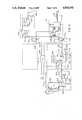
- FIG. 1illustrates the amplifier having digital bias control apparatus in block diagram form
- FIGS. 2-3illustrate various amplifying elements that can be used in the amplifier of FIG. 1;
- FIG. 4illustrates in flow diagram form the operational steps taken by the control processor to regulate the operating point of the amplifying elements.
- the amplifier having digital bias control apparatususes a processor to provide precise, dynamic control over the operating point of a plurality of amplifying elements in an amplifier.
- This processorcontrols each amplifying element to optimize the operating point of each individual amplifying element as a function of the amplifying element characteristics, the operating environment and the applied input signal.
- the use of a processorenables the user to remotely program the operating point of each individual amplifying element in the amplifier.
- the processorfurther enables dynamic changes in the operating characteristics of the amplifier as the operating environment of these amplifying elements changes.
- the processoralso can generate an alarm signal if any particular amplifying element is operating out of its nominal specifications.
- This digital bias control apparatuscan function in class A, AB, B or C type of amplifiers whether they are tuned or untuned and whether the amplifier operates in a pulsed or continuous mode.
- the digital bias control apparatus in the amplifieroperates by sequencing through the plurality of amplifying elements contained in the amplifier. Each individual amplifying element is selected by the digital bias control circuit and placed into a test mode in which the amplifying element is forward biased in the active mode with no input signal applied to the amplifying element. If the amplifier operates in a pulsed mode of operation, the test mode is activated in the intervals between applied input pulse signals. If the amplifier operates in the continuous mode a forced idle condition is imposed on this amplifying element in order to initiate the test mode. In the test mode, the processor reads a bias value from memory indicative of the desired bias for this particular amplifying element. The power source is regulated to supply this predefined bias signal to the selected amplifying element.
- the output signal from the amplifying elementis monitored to identify the operating point of this amplifying element in the active, forward biased, no input signal condition. If the measured values of bias signal and output signal do not match predetermined desired values as stored in the processor memory, the processor updates the predefined bias value that is stored in memory to therefore shift the nominal operating point of this amplifying element to compensate for dynamic changes in the operating environment or the operating characteristics inherent in this particular device.
- the use of a processor programmed with a control algorithmprovides both dynamic and precise control over the operating point of every amplifying element in an amplifier.
- the processorcontrols the bias signal applied to each amplifying element individually rather than according to a nominal and simplistic arrangement such as is obtained by the use of analog feedback circuitry found in the prior art.
- the processoralso controls the operating point of both vacuum tube and transistor amplifying elements.
- the processoris equipped with a remote access port that enables a user to reprogram the desired operating point or operating characteristics of the amplifying devices from a remote location or from a test panel in the amplifier circuit to compensate for changes in the code of the amplifying element used or to compensate for variations in the desired operating characteristics of the amplifier as a whole.
- a class A amplifieris one in which the operating point and the input signal are such that the current flows at all times in the output circuit of the amplifier, whether the collector, plate or drain electrode of the amplifying element.
- a class A amplifieroperates essentially over a linear portion of the amplifying element characteristic.
- a class B amplifieris one in which the operating point of the amplifying element is at an extreme end of its characteristic, so the quiescent power is very small and either the quiescent current or the quiescent voltage is approximately zero. If the input signal is sinusoidal, amplification takes place for only one-half a cycle of the sinusoidal input signal.
- a class AB amplifieris one operating between the two extremes defined for class A and class B amplifiers. Hence the output signal is zero for part but less than one half of an input sinusoidal signal cycle.
- a class C amplifieris one in which the operating point of the amplifying element is selected so that output current or voltage is zero for more than one half of an input sinusoidal signal cycle.
- a tuned amplifieris one in which the load placed on the amplifier is a tuned circuit that operates near its resonant frequency.
- a pulsed amplifier mode of operationis one in which a signal is only periodically applied to the input of the amplifier and the periods between pulse signals are ones in which no signal is applied to the amplifier.
- Continuous mode of operationis where the amplifier continually receives an input signal, which input signal is amplified by the amplifier. Even though an input signal in continuously applied to the amplifier, this input signal may be invariant for a significant period of time or may even be absent for periods of time. However the very nature of continuous mode of operation is that the absence of an input signal is irregular at best.
- the frequency classification for an amplifierindicates the range of frequencies that are amplified by this circuit.
- the circuit described belowis a radio frequency amplifier which is defined as covering input signals from a few kilohertz to hundreds of megahertz, therefore spanning a tremendous range of input signal frequencies.
- FIG. 1illustrates in block diagram form the general architecture of an amplifier equipped with the digital bias control apparatus of the present invention.
- This amplifieris a two stage amplifier consisting of: low power amplifier 102 and high power amplifier 103.
- the low power amplifier 102receives an input signal on lead 121 from a signal source (not shown) and amplifies this signal to a predefined output level and applies this amplified signal via lead 151 to the input of high power amplifier 103.
- the signal received from low power amplifier 102is amplified by high power amplifier 103 into a predetermined high power output signal which is output on lead 152 to a load (not shown).
- FIG. 1A typical use of such an amplifier as is illustrated in FIG. 1 is in the field of linear pulse amplifier applications, such as magnetic resonance imaging (MRI) systems.
- MRImagnetic resonance imaging
- Such a systemis the MRI-20K Series Magnetic Resonance Imaging Amplifier manufactured by Erbtec Engineering, Inc.
- the MRI systemtypically has three imaging modes of operation.
- the MRI systemrequires the amplifier to output a tune-up signal to align the antenna circuitry within the magnet core in preparation for imaging.
- a second mode of operationis called the head mode which requires a much higher power level output to perform imaging on the head of the individual being tested.
- the final or third mode of operationis the body mode where still higher power levels are required to obtain an image of the denser, more complicated body of the individual being tested by this apparatus. It is obvious that the output power of the MRI amplifier must be precisely controlled in order to obtain the requisite data output required of this system.
- the amplifier illustrated in FIG. 1 as the preferred embodiment of the inventionconsists of a radio frequency, tuned high power amplifier system operating in the pulsed mode.
- the amplifying elements in low power amplifier 102are typically field effect transistor devices, while the high power amplifier 103 is equipped with vacuum tube devices to obtain the high levels of radio frequency power required for this application.
- Controller 101In order to precisely control the operating point of each amplifying element in this amplifier, controller 101 is provided to test, monitor and regulate the bias signal applied to the amplifying elements in low power amplifier 102 and high power amplifier 103 as disclosed in detail herein below.
- Controller 101consists of a control processor 111 having a remote access port 119 that is connected to an optional control panel (not shown) or that can be accessed via a remote dial up telephone link that is well known in the art.
- Control processor 111outputs control, data and address signals on bus 116 to regulate the operation of digital input/output circuit 112, analog interface 113 and bias control circuit 114 which are all connected to bus 116.
- Digital input/output circuit 112contains a plurality of digital interface circuits that exchange control signals with the various elements in low power amplifier 102 and high power amplifier 103 to control the operation of these two amplifier stages.
- Analog interface 113obtains analog data from the amplifier stages in order to measure and monitor the various environmental and operational characteristics of low power amplifier 102 and high power amplifier 103. Included in the characteristics monitored by analog interface 113 are the temperature of operation of the various amplifying elements, the power output of the amplifier stages, the output signal from the various amplifying elements as well as power supply voltages, environmental conditions, etc.
- Bias control circuit 114produces the bias control signal for each amplifying element in low power amplifier 102 and high power amplifier 103 under the control of control processor 111.
- Control processor 111stores data in memory 115 indicative of the desired operating point of each amplifying element in the amplifier as well as data concerning the environmental and operating conditions of the amplifier.
- Memory 115is typically implemented using several different types of devices.
- a ROMis used to store the operating program and an electrically alterable ROM (EPROM) stores the amplifying element target bias values.
- EPROMelectrically alterable ROM
- Low power amplifier 102receives high frequency, pulsed input signals on signal lead 121 from an input source (not shown). Resistors 122-124 and operational amplifier 125 perform a well-known input signal conditioning function and applied the modified input signal to the power amplifying segment 161 of low power amplifier 102.
- the function of power amplifying segment 161is to amplify the applied input signal and output this signal via impedance matching circuit 128 to output lead 151.
- the operation of the power amplifying segment 161is controlled by bias generator 117.
- Monitor 129measures various operational parameters of power amplifying segment 161 as well as environmental conditions within low power amplifier 102.
- FIG. 1illustrates an amplifier configuration that consists of two series connected amplifier stages 126, 127 located within power amplifying segment 161. Each of these two amplifier stages 126, 127 includes two active amplifying elements 224, 226, each driven by associated bias generators 117-1, 117-2, respectively.
- bias generator 117-1is provided since it is identical in structure to bias generator 117-2.
- the bias generator functionis divided into two parts, a first segment designated bias control 114 that is part of the circuitry in controller 101 and bias generator 117-1 which is contained in low power amplifier 102. It is obvious that the distribution of elements shown in FIG. 2 is an arbitrary selection for design convenience and in no way should limit the concepts embodied therein.
- Bias control circuit 114contains a digital to analog converter circuit 201 which is connected to bus 116 and is responsive to a bias signal value, typically in the form of an eight bit digital signal, applied thereto by control processor 111 to generate an analog signal that is indicative of the bias signal applied to amplifying element 224.
- Digital to analog convertor 201also contains a clock input labeled C which receives a select signal from processor 111 that enables control processor 111 to specifically activate amplifying element 224.
- input OC on digital to analog converter 201is used as an on/off switch, again under the control of control processor 111, to switch amplifying element 224 on or off.
- the analog signal produced by digital to analog converter 201 in response to the bias value signals applied to bus 116 by control processor 111is applied to the non-inverting input of differential amplifier 203.
- a filter capacitor 202is provided between the digital to analog convertor 201 and amplifier 203 to reduce transients on this signal lead.
- Differential amplifier 203includes feedback resistor 204 and bias resistor 205 to produce a bias drive signal that is applied through an RC filter consisting of resistors 206, 208 and capacitor 207 to output lead 143-1. This analog signal applied to signal lead 143-1 travels from bias control 114 of controller 101 to bias generator 117-1 contained in low power amplifier 102.
- the analog drive signal appearing on lead 143-1is applied through an RC filter consisting of resistors 209, 211 and capacitor 210 to the non-inverting input of comparator 212.
- the inverting input of comparator 212is connected via lead 141-1 to control processor 111.
- Comparator 212activates bias generator 117-1 in response to signals applied to the inverting and noninverting inputs of comparator 212.
- Comparator 212, amplifier 217 and their associated resistors 213, 215, 216convert the received bias signal into a bias signal that is applied through an RC filter consisting of resistors 219, 221 and capacitor 220 to the gate input of field effect transistor device 224.
- Amplifying element 127consists of field effect transistor devices 224, 226 and their associated AC bias devices (resistor 222, capacitor 223 and resistor 228, capacitor 227, respectively).
- Field effect transistors 224 and 226are interconnected with each other, the power source, and the RF output lead 151 via a transformer circuit consisting of impedance matching element 128.
- the impedance matching element 128consists of transformers 236, 237 and 238 interconnected as shown in FIG. 2. This is a well known tuned circuit output configuration for matching the impedance of the amplifier stage 127 with the output load.
- Bias circuit 117-1applies a predesignated bias to the gate terminal of field effect transistor 224 to bias this device in the active region at a predetermined operating point.
- the signal to be amplifiedis applied from the previous amplifying stage 126 via an impedance matching circuit 236.
- Field effect transistors 224 and 226amplify the signal applied through impedance matching circuit 236 and output the amplified signal over the RF output signal lead 151.
- the power drawn by field effect transistors 224 and 226 through impedance matching circuit 128is monitored by a current monitor circuit 240 that is part of monitor circuit 129.
- the current monitor circuit 240consists of a sense resistor 230 connected in series between the power source Vd and the power lead that is connected to impedance matching circuit 128.
- the voltage generated across sense resistor 230 by the current flowing therethroughis sensed by differential amplifier 233 with its associated resistors 231, 232.
- the amount of current drawn by the amplifier 127 through resistor 230is converted into a sense signal by differential amplifier 233 and applied to field effect transistor 234 which generates a voltage by the application of current to resistor 235, which voltage is indicative of the amount of current drawn by the amplifier 127 through sense resistor 230.
- bias circuits 117-1 and 117-2apply a bias signal to field effect transistors 224, 226 to establish the operating point of this device.
- the AC input signalwhich is an RF frequency signal, is applied through impedance matching circuit 236 to the gate of transistors 224, 226.
- Transistor 224in conjunction with transistor 226, amplifies the input signal applied through the impedance matching circuit 236 and outputs the amplified signal on lead 151.
- Current monitoring circuit 240provides a voltage on lead 142-1 to analog interface 113 that is indicative of the current drawn by the amplifier circuit 127 at any instant in time.
- the dynamic bias level set operationcan be divided into two steps: dynamic bias set and dynamic bias refresh.
- the dynamic bias set steptakes place for vacuum tube amplifying elements just as the amplifier is about to enter the full readiness state (OPERATE mode) and for FET amplifying elements as the amplifier enters STANDBY mode.
- processor 111loads a target bias signal value from the ROM device in memory 115 to the RAM device in memory 115 for each amplifying element.
- the bias control operationillustrated in FIG. 4, is then implemented to establish the optimum or selected operating point for each amplifying element in sequence.
- the dynamic bias refresh stepis analogous to the dynamic bias set step and is used for FET amplifying elements to continually finely adjust their operating point. Any fluctuation in FET operation affects amplifier performance and these devices are very sensitive to temperature and voltage fluctuations. Therefore, processor 111 periodically monitors and finely adjusts the bias of these devices.
- the dynamic bias refresh stepis invoked on a periodic basis during the STANDBY mode and between externally generated UNBLANK signals during the OPERATE mode.
- UNBLANKrefers to a signal that enables an amplifying element to amplify an RF pulse input signal, although it does not imply the presence of an RF pulse on the input of the amplifying element.
- FIG. 4In order to illustrate the functioning of the Bias Level Set Operation, the flowchart of FIG. 4 is used to describe, on a step by step basis, the operation of the circuitry of FIGS. 1-3. The following description is of a typical dynamic bias set step for the FET amplifying elements of FIG. 2.
- control processor 111initiates the bias control routine at step 401 and initializes a counter at step 402, so that each of the n amplifying elements located in the amplifier are screened in sequence.
- processor 111reads a predetermined operating point value from memory 115 that is indicative of the bias signal that must be applied to the gate terminal of field effect transistor 224 to bias this device at the designated operating point.
- processor 111determines whether the amplifier is in the STANDBY mode or in an intrapulse interval in the OPERATE mode. If not, the amplifier is processing an input signal and a bias set or refresh operation cannot take place so the processor must exit this process. If processor 111 determines that this operation can proceed, it disables the external RF signal at step 405 by deactivating input amplifier 125.
- Control processor 111at step 406 outputs an eight bit digital signal on bus 116 that is indicative of the drive signal that must be applied to the gate terminal of field effect transistor 224. This eight bit signal is converted by digital to analog converter 201 into an analog signal that is proportional to the bias signal that must be applied to the gate of field effect transistor 224. Control processor 111 selects digital to analog converter 201 by placing a signal on the clock input of this device to cause the eight bit signal on bus 116 to be loaded therein. Control processor 111 also unblanks this amplifying element at step 407 by applying an enable signal on lead 141-1.
- control processor 111can select digital to analog converter 201 by the use of this select signal while disabling all the other bias generator circuits so that only the operating point of field effect transistor 224 is established during this test cycle.
- the analog signal output by digital to analog converter 201is transformed and transmitted by bias control circuit 114 and bias generator circuit 117-1 and applied to the gate terminal of field effect transistor 224.
- the current drawn by field effect transistor 224 as a result of the application of this predetermined bias signalis measured at step 408 by current monitor circuit 240.
- processor 111can specifically enable, in very controlled fashion, the amplifying element 224 contained within amplifier stage 127 and monitor the operation of this device with all of the other amplifying elements in the amplifier placed in an inactive or cutoff mode.
- the current measured by current monitoring circuit 240 at step 408is transmitted to control processor 111 via bus 142 through analog interface circuit 113.
- Control processor 111 BLANKSthis amplifying element at step 409.
- the analog signal output by current monitor circuit 240is converted by analog interface 113 into an eight bit digital signal in well known fashion. This eight bit digital signal is read by control processor 111 via bus 116 at step 410 and compared to device characteristic information that is stored in memory 115.
- This device characteristic informationis indicative of the current drawn by a field effect transistor of the type used to implement device 224 in response to a predetermined bias signal.
- Control processor 111can therefore drive the exact operating point of field effect transistor 224 based on the bias signal applied to the gate terminal thereof and the measured drain current drawn by this device in response to that bias signal.
- processor 111changes the input bias at step 411. This is accomplished by processor 111 modifying the eight bit digital input bias signal value stored in memory 115. Therefore, the input bias generated by bias control 114 and bias generator 117-1 is adjusted to control the operating point of amplifying element 224.
- the variable iis incremented and compared with n at step 413 to determine whether all of the amplifying elements have been tested and the bias signal values refreshed.
- the periodically revised bias signal valuesare written into the RAM portion of memory 115. Any revision of these values that is of a permanent nature can be accomplished via the remote access port 119. These revisions activate memory control circuitry (not shown) that changes the data stored in the EPROM device in memory 115.
- Control processor 111in response to the measured drain current and applied bias signal as well as other operational parameters that are measured by various sensors within the system (such as operating temperature, power supply voltages, etc.), can determine whether the operating point of field effect transistor 224 is to be adjusted. If the measured operating point and associated environmental parameters differ from a desired set of values by greater than a predesignated amount, control processor 111 generates a new value for the bias signal that is applied to field effect transistor 224.
- This new valueis written into memory 115 in place of the originally stored value and also transmitted to digital to analog converter 201 where it is stored for use by amplifier 127 in maintaining field effect transistor 224 in its desired operating point.
- the other amplifying elements contained within power amplifier segment 161are controlled in this fashion.
- the above described low power amplifier 102used field effect transistors as the amplifying elements although bipolar transistor could have been used in a similar configuration.
- the digital bias control apparatusalso functions in an environment where the amplifying element consists of a vacuum tube.
- FIG. 3illustrates the application of this digital bias control apparatus to a vacuum tube amplifying element.
- High power amplifier 103serves to provide a second level of amplification to the input signals applied to input lead 121.
- the once amplified input signals, output by low power amplifier 102 on lead 151,are amplified by power amplifying segment 162 and output via impedance matching circuit 134 to the RF output lead 152.
- the operation of the amplifying elements 132-1 to 132-6 contained within power amplifying segment 162are regulated by bias generator 118.
- Monitor circuit 135measures various operational parameters of power amplifying segment 162 as well as environmental conditions within high power amplifier 103.
- Power amplifying segment 162is illustrated as containing a plurality of parallel connected amplifying elements 131-1 to 131-6 6.
- the input signal on lead 151is divided by power splitter 131 and applied equally to each of the amplifying elements 131-1 to 131-6.
- the output of the amplifying elements 131-1 to 131-6are combined by power combiner 133 and applied to impedance matching circuit 134.
- all of power amplifying segment 162is illustrated as a two amplifying element embodiment shown in FIG. 3.
- bias control circuitry labeled 114is identical in function to that described above with respect to FIG. 2.
- a bias signal value in the form of a digital eight bit signalis applied to the input of digital to analog converter 331 and an analog signal representative of the bias signal is output therefrom to bias generator 118 contained within high power amplifier 103.
- This analog signalis applied through RC filter consisting of resistors 339, 341 and capacitor 340 to the inverting input of differential amplifier 344.
- An AC feedback RC combinationconsisting of resistor 342 and capacitor 343 connects the output of differential amplifier 344 with the inverting input in well known fashion.
- the non-inverting input of differential amplifier 344is connected to a bias source V.
- the voltage Vis applied through resistor 349, capacitor 348 and the scaling resistors 345, 346 to the non-inverting input of differential amplifier 344.
- Thisestablishes a DC feedback level for differential amplifier 344 and results in a regulated tube bias voltage stored on capacitor 348.
- Amplifier 344controls FET 353 to regulate the tube bias voltage on capacitor 348.
- the bias voltage capacitor 348does not vary with the application of the UNBLANK signal to isolation driver circuit 350, but is set by bias control circuit 114.
- FET 347when enabled by the signal appearing on lead 143-2, FET 347 applies the cathode/grid bias signal derived from bias control circuit 114 and stored on capacitor 348 to the cathode of this amplifying vacuum tube.
- Transistor 353regulates the voltage on capacitor 348.
- Field effect transistor 347is driven by the un-blank signal on lead 141-2 through isolated drive circuit 350 and switches the bias to vacuum tube amplifier 371.
- field effect transistor 347controls the amount of bias current applied to the cathode terminal of vacuum tube amplifier 371.
- the RF drive signalis applied through input matching impedance 351 to the cathode terminal of vacuum tube amplifier 371.
- Floating high voltage power supply 301applies a high level voltage signal through impedance transformer and power combiner circuit 133 to the anode terminal of vacuum tube 371.
- the other terminal of power supply 301is connected through sense resistor 311 to the cathode terminal of vacuum tube 371.
- the grid terminal of vacuum tube 371is grounded.
- Bias switch transistor 347applies a controllable amount of bias voltage on capacitor 348 voltage on the cathode terminal therefore controlling the vacuum tube's plate current.
- the amount of current drawn by vacuum tube 371is monitored by current monitor circuit 135.
- This circuitfunctions in similar fashion the current monitor circuit 240 disclosed above.
- the current drawn by the vacuum tube 371 through current sense resistor 311is monitored by differential amplifier 321.
- the voltage on either side of resistor 311is applied to the inverting input of differential amplifier 321 by devices 312-316 and to the non-inverting input of differential amplifier 321 by devices 317-320.
- Feedback resistors 322 and 323set the operating point of differential amplifier 321.
- the voltage across sense resistor 311is amplified by differential amplifier 321 and applied through resistor 324 and clamping diodes 325, 326 to an RC filter consisting of resistor 327 and capacitor 328.
- the output of this RC filteris applied through analog to digital converter 329 which is part of analog interface 113 where it is converted into an eight bit digital signal and read at the control processor over its I/0 bus 116.
- this vacuum tube amplifiercan be placed in a test mode in the interval between signal pulses by the use of the enable select lead controlled by UNBLANK.
- a predetermined bias signal valuehas been read out of memory 115 by control processor 111 and transmitted over bus 116 to digital to analog converter 331.
- the digital bias signal value so obtained from control processor 111is converted to an analog signal and transmitted to vacuum tube 371 by bias generator 118.
- the current drawn by vacuum tube 371 in the no input signal modeis sensed by current monitor 303 and this value is returned to control processor 111 via the analog interface 113.
- the bias applied to the cathode terminal of vacuum tube 371is sensed by floating grid current monitor circuit 135 and is transmitted to the analog interface circuit 114 where it is converted to a digital signal and output on bus 116 to control processor 111.
- monitor circuits 129, 135are described in part above. These circuits not only monitor the output signals of the amplifying elements but also measure various environmental parameters within low and high power amplifiers 102, 103. For example, the operating temperature of the field effect transistor devices in low power amplifier 102 can be measured in well known fashion. Memory 115 can include temperature/operating point data that indicates to processor 111 the modifications required to the operating point of the field effect transistors as a function of variations in operating temperature. Similar environmental factors can be considered by processor 111 in regulating the operating point of all of the amplifier elements.
Landscapes
- Engineering & Computer Science (AREA)
- Power Engineering (AREA)
- Amplifiers (AREA)
Abstract
Description
Claims (11)
Priority Applications (1)
| Application Number | Priority Date | Filing Date | Title |
|---|---|---|---|
| US07/340,385US4924191A (en) | 1989-04-18 | 1989-04-18 | Amplifier having digital bias control apparatus |
Applications Claiming Priority (1)
| Application Number | Priority Date | Filing Date | Title |
|---|---|---|---|
| US07/340,385US4924191A (en) | 1989-04-18 | 1989-04-18 | Amplifier having digital bias control apparatus |
Publications (1)
| Publication Number | Publication Date |
|---|---|
| US4924191Atrue US4924191A (en) | 1990-05-08 |
Family
ID=23333140
Family Applications (1)
| Application Number | Title | Priority Date | Filing Date |
|---|---|---|---|
| US07/340,385Expired - LifetimeUS4924191A (en) | 1989-04-18 | 1989-04-18 | Amplifier having digital bias control apparatus |
Country Status (1)
| Country | Link |
|---|---|
| US (1) | US4924191A (en) |
Cited By (66)
| Publication number | Priority date | Publication date | Assignee | Title |
|---|---|---|---|---|
| US5060294A (en)* | 1990-07-05 | 1991-10-22 | Motorola, Inc. | Dual mode power amplifier for radiotelephone |
| US5093667A (en)* | 1989-10-16 | 1992-03-03 | Itt Corporation | T/R module with error correction |
| US5179332A (en)* | 1991-08-16 | 1993-01-12 | General Electric Company | NMR radio frequency coil with disable circuit |
| US5278404A (en)* | 1992-07-20 | 1994-01-11 | At&T Bell Laboratories | Optical sub-system utilizing an embedded micro-controller |
| US5281925A (en)* | 1992-11-17 | 1994-01-25 | Acrodyne Industries, Inc. | RF amplifier providing reduced drive response rise times and fall times |
| DE4228833A1 (en)* | 1992-08-29 | 1994-03-03 | Thomson Brandt Gmbh | Signal processing circuit balancing method - using circuit with one stage always operating normally, while another stage is balanced |
| US5361403A (en)* | 1990-11-14 | 1994-11-01 | Ericsson Ge Mobile Communication Holding, Inc. | AM-FM transmitter power amplifier |
| GB2282291A (en)* | 1989-10-16 | 1995-03-29 | Int Standard Electric Corp | Amplifier circuit |
| US5423078A (en)* | 1993-03-18 | 1995-06-06 | Ericsson Ge Mobile Communications Inc. | Dual mode power amplifier for analog and digital cellular telephones |
| US5432473A (en)* | 1993-07-14 | 1995-07-11 | Nokia Mobile Phones, Limited | Dual mode amplifier with bias control |
| US5451907A (en)* | 1994-05-16 | 1995-09-19 | Eni, Div. Of Astec America, Inc. | Active bias for a pulsed power amplifier |
| US5479499A (en)* | 1993-12-15 | 1995-12-26 | Murata Manufacturing Co., Ltd. | Sensor circuit for voice/fax switch with cascaded amplifier circuit |
| US5493255A (en)* | 1995-03-21 | 1996-02-20 | Nokia Mobile Phones Ltd. | Bias control circuit for an RF power amplifier |
| US5530923A (en)* | 1994-03-30 | 1996-06-25 | Nokia Mobile Phones Ltd. | Dual mode transmission system with switched linear amplifier |
| US5537080A (en)* | 1995-06-06 | 1996-07-16 | Chawla; Yogendra K. | Gain stability arrangement for HV MOSFET power amplifier |
| US5548616A (en)* | 1994-09-09 | 1996-08-20 | Nokia Mobile Phones Ltd. | Spread spectrum radiotelephone having adaptive transmitter gain control |
| US5589796A (en)* | 1994-11-01 | 1996-12-31 | Motorola, Inc | Method and apparatus for increasing amplifier efficiency |
| WO1998038733A1 (en)* | 1997-02-26 | 1998-09-03 | Ericsson Inc. | Flexible current control in power amplifiers |
| US5831476A (en)* | 1996-12-02 | 1998-11-03 | Motorola, Inc. | Voltage-tuned millimeter-wave amplifier and method for tuning |
| GB2334167A (en)* | 1998-02-07 | 1999-08-11 | Motorola Ltd | Drain current control circuit for RF MOSFET amplifier |
| US5994955A (en)* | 1998-06-26 | 1999-11-30 | Maxim Integrated Products, Inc. | Driver amplifiers with low noise standby mode characteristics |
| US6006109A (en)* | 1996-05-07 | 1999-12-21 | Samsung Electronics Co., Ltd. | Wireless data communication system using a microphone/headphone jack of a portable phone |
| US6160449A (en)* | 1999-07-22 | 2000-12-12 | Motorola, Inc. | Power amplifying circuit with load adjust for control of adjacent and alternate channel power |
| US6166598A (en)* | 1999-07-22 | 2000-12-26 | Motorola, Inc. | Power amplifying circuit with supply adjust to control adjacent and alternate channel power |
| US6349216B1 (en) | 1999-07-22 | 2002-02-19 | Motorola, Inc. | Load envelope following amplifier system |
| US20020055349A1 (en)* | 2000-09-11 | 2002-05-09 | Xytrans, Inc. | Self-tuned millimeter wave RF Transceiver module |
| US6438360B1 (en) | 1999-07-22 | 2002-08-20 | Motorola, Inc. | Amplifier system with load control to produce an amplitude envelope |
| US6480061B2 (en) | 1999-01-13 | 2002-11-12 | Nortel Networks Limited | Amplifier having digital micro processor control apparatus |
| US6556084B2 (en)* | 2000-12-18 | 2003-04-29 | Koninklijke Philips Electronics N.V. | Linearized class C amplifier with dynamic biasing |
| EP1367710A1 (en)* | 2002-05-31 | 2003-12-03 | Telefonaktiebolaget L M Ericsson (Publ) | Power amplifiers |
| US6661394B1 (en)* | 1999-04-17 | 2003-12-09 | Lg Electronics Inc. | Driving circuit for radio frequency plasma display panel |
| EP1387485A1 (en)* | 2002-08-01 | 2004-02-04 | Telefonaktiebolaget L M Ericsson (Publ) | Circuit for power amplification |
| US6716677B2 (en) | 2000-09-11 | 2004-04-06 | Xytrans, Inc. | Microwave monolithic integrated circuit package |
| WO2004013957A3 (en)* | 2002-08-01 | 2004-05-21 | Ericsson Telefon Ab L M | Circuit for power amplification |
| US6990682B1 (en)* | 1999-06-29 | 2006-01-24 | Fujitsu Limited | Two-way CATV system |
| US20070026812A1 (en)* | 2005-07-27 | 2007-02-01 | Harris Corporation | Power level control for RF transmitters |
| US20080042744A1 (en)* | 2006-08-15 | 2008-02-21 | Soung Whan Chung | Output circuit of vacuum-tube amplifier |
| US20090021414A1 (en)* | 2005-05-18 | 2009-01-22 | Bosch Rexroth D.S.I. | Remote Control for Mobile Machine, In Particular for Public Works Machine, Agricultural or Load-Handling Machine |
| US20090036171A1 (en)* | 2007-07-30 | 2009-02-05 | Telefonaktiebolaget Lm Ericsson (Publ) | Efficient Storing of Backoff and Crestcomp Values |
| CZ303920B6 (en)* | 2009-06-26 | 2013-06-26 | Ceské vysoké ucení technické v Praze | Device for automatic control and adjustment of power active elements, particularly in power solid-state amplifiers |
| US20140191807A1 (en)* | 2013-01-08 | 2014-07-10 | Aviat U.S., Inc. | Systems and methods for biasing amplifiers with adaptive closed loop control |
| US20150117667A1 (en)* | 2013-10-30 | 2015-04-30 | Harman Becker Automotive Systems Gmbh | Infotainment system |
| US9059666B2 (en) | 2013-01-08 | 2015-06-16 | Aviat U.S., Inc. | Systems and methods for biasing amplifiers during high-power operation with adaptive closed-loop control |
| US9160284B2 (en) | 2013-01-08 | 2015-10-13 | Aviat U.S., Inc. | Systems and methods for biasing amplifiers using adaptive closed-loop control and adaptive predistortion |
| EP3599719A1 (en)* | 2018-07-25 | 2020-01-29 | Rohde & Schwarz GmbH & Co. KG | A broadband high power amplifier |
| US11101108B2 (en) | 2018-07-27 | 2021-08-24 | Eagle Harbor Technologies Inc. | Nanosecond pulser ADC system |
| US11159156B2 (en) | 2013-11-14 | 2021-10-26 | Eagle Harbor Technologies, Inc. | High voltage nanosecond pulser |
| US11171568B2 (en) | 2017-02-07 | 2021-11-09 | Eagle Harbor Technologies, Inc. | Transformer resonant converter |
| US11222767B2 (en)* | 2018-07-27 | 2022-01-11 | Eagle Harbor Technologies, Inc. | Nanosecond pulser bias compensation |
| US11227745B2 (en) | 2018-08-10 | 2022-01-18 | Eagle Harbor Technologies, Inc. | Plasma sheath control for RF plasma reactors |
| US11302518B2 (en) | 2018-07-27 | 2022-04-12 | Eagle Harbor Technologies, Inc. | Efficient energy recovery in a nanosecond pulser circuit |
| US11387076B2 (en) | 2017-08-25 | 2022-07-12 | Eagle Harbor Technologies, Inc. | Apparatus and method of generating a waveform |
| US11404246B2 (en) | 2019-11-15 | 2022-08-02 | Eagle Harbor Technologies, Inc. | Nanosecond pulser bias compensation with correction |
| US11430635B2 (en) | 2018-07-27 | 2022-08-30 | Eagle Harbor Technologies, Inc. | Precise plasma control system |
| US11502672B2 (en) | 2013-11-14 | 2022-11-15 | Eagle Harbor Technologies, Inc. | High voltage nanosecond pulser with variable pulse width and pulse repetition frequency |
| US11527383B2 (en) | 2019-12-24 | 2022-12-13 | Eagle Harbor Technologies, Inc. | Nanosecond pulser RF isolation for plasma systems |
| US11532457B2 (en) | 2018-07-27 | 2022-12-20 | Eagle Harbor Technologies, Inc. | Precise plasma control system |
| US11539352B2 (en) | 2013-11-14 | 2022-12-27 | Eagle Harbor Technologies, Inc. | Transformer resonant converter |
| US11631573B2 (en) | 2014-02-28 | 2023-04-18 | Eagle Harbor Technologies, Inc. | High voltage resistive output stage circuit |
| US11646176B2 (en) | 2019-01-08 | 2023-05-09 | Eagle Harbor Technologies, Inc. | Efficient nanosecond pulser with source and sink capability for plasma control applications |
| US11670484B2 (en) | 2018-11-30 | 2023-06-06 | Eagle Harbor Technologies, Inc. | Variable output impedance RF generator |
| US11689107B2 (en) | 2014-02-28 | 2023-06-27 | Eagle Harbor Technologies, Inc. | Nanosecond pulser bias compensation |
| US12230477B2 (en) | 2018-07-27 | 2025-02-18 | Eagle Harbor Technologies, Inc. | Nanosecond pulser ADC system |
| US12348228B2 (en) | 2022-06-29 | 2025-07-01 | EHT Ventures LLC | Bipolar high voltage pulser |
| US12354832B2 (en) | 2022-09-29 | 2025-07-08 | Eagle Harbor Technologies, Inc. | High voltage plasma control |
| US12437967B2 (en) | 2020-07-09 | 2025-10-07 | Eagle Harbor Technologies, Inc. | Ion current droop compensation |
Citations (10)
| Publication number | Priority date | Publication date | Assignee | Title |
|---|---|---|---|---|
| US3497822A (en)* | 1968-05-10 | 1970-02-24 | Bell Telephone Labor Inc | Bias control circuit for pulse power transistor amplifiers to stabilize the quiescent current therein |
| US4345215A (en)* | 1979-08-31 | 1982-08-17 | Hitachi, Ltd. | Audio frequency power amplifier circuit |
| US4366447A (en)* | 1981-01-22 | 1982-12-28 | Pioneer Electronic Corporation | Push-pull amplifier circuit |
| US4414477A (en)* | 1981-09-09 | 1983-11-08 | Mewburn Crook Anthony J S | Wind energy convertor |
| US4435652A (en)* | 1981-05-26 | 1984-03-06 | Honeywell, Inc. | Threshold voltage control network for integrated circuit field-effect trransistors |
| US4458213A (en)* | 1982-12-13 | 1984-07-03 | Sony Corporation | Constant quiescent current, class AB amplifier output stage |
| US4459553A (en)* | 1982-02-11 | 1984-07-10 | Tektronix, Inc. | D.C. Stabilization circuit for a follower-type amplifier |
| US4538114A (en)* | 1982-09-03 | 1985-08-27 | Hitachi, Ltd. | Differential amplifier |
| US4623786A (en)* | 1984-11-07 | 1986-11-18 | At&T Bell Laboratories | Transimpedance amplifier with overload protection |
| US4751472A (en)* | 1985-11-19 | 1988-06-14 | Herfurth Gmbh | High frequency amplifier |
- 1989
- 1989-04-18USUS07/340,385patent/US4924191A/ennot_activeExpired - Lifetime
Patent Citations (10)
| Publication number | Priority date | Publication date | Assignee | Title |
|---|---|---|---|---|
| US3497822A (en)* | 1968-05-10 | 1970-02-24 | Bell Telephone Labor Inc | Bias control circuit for pulse power transistor amplifiers to stabilize the quiescent current therein |
| US4345215A (en)* | 1979-08-31 | 1982-08-17 | Hitachi, Ltd. | Audio frequency power amplifier circuit |
| US4366447A (en)* | 1981-01-22 | 1982-12-28 | Pioneer Electronic Corporation | Push-pull amplifier circuit |
| US4435652A (en)* | 1981-05-26 | 1984-03-06 | Honeywell, Inc. | Threshold voltage control network for integrated circuit field-effect trransistors |
| US4414477A (en)* | 1981-09-09 | 1983-11-08 | Mewburn Crook Anthony J S | Wind energy convertor |
| US4459553A (en)* | 1982-02-11 | 1984-07-10 | Tektronix, Inc. | D.C. Stabilization circuit for a follower-type amplifier |
| US4538114A (en)* | 1982-09-03 | 1985-08-27 | Hitachi, Ltd. | Differential amplifier |
| US4458213A (en)* | 1982-12-13 | 1984-07-03 | Sony Corporation | Constant quiescent current, class AB amplifier output stage |
| US4623786A (en)* | 1984-11-07 | 1986-11-18 | At&T Bell Laboratories | Transimpedance amplifier with overload protection |
| US4751472A (en)* | 1985-11-19 | 1988-06-14 | Herfurth Gmbh | High frequency amplifier |
Cited By (99)
| Publication number | Priority date | Publication date | Assignee | Title |
|---|---|---|---|---|
| GB2282291A (en)* | 1989-10-16 | 1995-03-29 | Int Standard Electric Corp | Amplifier circuit |
| US5093667A (en)* | 1989-10-16 | 1992-03-03 | Itt Corporation | T/R module with error correction |
| WO1992016048A1 (en)* | 1989-10-16 | 1992-09-17 | Itt Corporation | T/r module with error correction |
| GB2258763A (en)* | 1989-10-16 | 1993-02-17 | Int Standard Electric Corp | T/r module with error correction |
| GB2258763B (en)* | 1989-10-16 | 1995-08-09 | Int Standard Electric Corp | T/R Module with error correction |
| GB2282291B (en)* | 1989-10-16 | 1995-08-09 | Int Standard Electric Corp | Amplifier circuit |
| US5060294A (en)* | 1990-07-05 | 1991-10-22 | Motorola, Inc. | Dual mode power amplifier for radiotelephone |
| US5361403A (en)* | 1990-11-14 | 1994-11-01 | Ericsson Ge Mobile Communication Holding, Inc. | AM-FM transmitter power amplifier |
| US5423074A (en)* | 1990-11-14 | 1995-06-06 | Ericsson Ge Mobile Communications Inc. | AM-FM transmitter power amplifier |
| US5179332A (en)* | 1991-08-16 | 1993-01-12 | General Electric Company | NMR radio frequency coil with disable circuit |
| US5396059A (en)* | 1992-07-20 | 1995-03-07 | At&T Corp. | Digital processor-controlled arrangement for monitoring and modifying system operating parameters |
| US5278404A (en)* | 1992-07-20 | 1994-01-11 | At&T Bell Laboratories | Optical sub-system utilizing an embedded micro-controller |
| DE4228833A1 (en)* | 1992-08-29 | 1994-03-03 | Thomson Brandt Gmbh | Signal processing circuit balancing method - using circuit with one stage always operating normally, while another stage is balanced |
| DE4228833B4 (en)* | 1992-08-29 | 2006-03-30 | Deutsche Thomson-Brandt Gmbh | Signal processing circuit |
| US5281925A (en)* | 1992-11-17 | 1994-01-25 | Acrodyne Industries, Inc. | RF amplifier providing reduced drive response rise times and fall times |
| US5423078A (en)* | 1993-03-18 | 1995-06-06 | Ericsson Ge Mobile Communications Inc. | Dual mode power amplifier for analog and digital cellular telephones |
| US5432473A (en)* | 1993-07-14 | 1995-07-11 | Nokia Mobile Phones, Limited | Dual mode amplifier with bias control |
| US5479499A (en)* | 1993-12-15 | 1995-12-26 | Murata Manufacturing Co., Ltd. | Sensor circuit for voice/fax switch with cascaded amplifier circuit |
| US5530923A (en)* | 1994-03-30 | 1996-06-25 | Nokia Mobile Phones Ltd. | Dual mode transmission system with switched linear amplifier |
| US5451907A (en)* | 1994-05-16 | 1995-09-19 | Eni, Div. Of Astec America, Inc. | Active bias for a pulsed power amplifier |
| US5548616A (en)* | 1994-09-09 | 1996-08-20 | Nokia Mobile Phones Ltd. | Spread spectrum radiotelephone having adaptive transmitter gain control |
| US5589796A (en)* | 1994-11-01 | 1996-12-31 | Motorola, Inc | Method and apparatus for increasing amplifier efficiency |
| CN1074609C (en)* | 1994-11-01 | 2001-11-07 | 摩托罗拉公司 | Method and device for improving efficiency of amplitude |
| US5493255A (en)* | 1995-03-21 | 1996-02-20 | Nokia Mobile Phones Ltd. | Bias control circuit for an RF power amplifier |
| US5537080A (en)* | 1995-06-06 | 1996-07-16 | Chawla; Yogendra K. | Gain stability arrangement for HV MOSFET power amplifier |
| US6006109A (en)* | 1996-05-07 | 1999-12-21 | Samsung Electronics Co., Ltd. | Wireless data communication system using a microphone/headphone jack of a portable phone |
| US5831476A (en)* | 1996-12-02 | 1998-11-03 | Motorola, Inc. | Voltage-tuned millimeter-wave amplifier and method for tuning |
| US6072995A (en)* | 1997-02-26 | 2000-06-06 | Ericsson Inc. | Flexible current control in power amplifiers |
| WO1998038733A1 (en)* | 1997-02-26 | 1998-09-03 | Ericsson Inc. | Flexible current control in power amplifiers |
| GB2334167A (en)* | 1998-02-07 | 1999-08-11 | Motorola Ltd | Drain current control circuit for RF MOSFET amplifier |
| GB2334167B (en)* | 1998-02-07 | 2002-09-11 | Motorola Ltd | Amplifying circuit and method for determining optimal bias voltages therein |
| WO2000001064A1 (en)* | 1998-06-26 | 2000-01-06 | Maxim Integrated Products, Inc. | Driver amplifiers with low noise standby mode characteristics |
| US5994955A (en)* | 1998-06-26 | 1999-11-30 | Maxim Integrated Products, Inc. | Driver amplifiers with low noise standby mode characteristics |
| US6480061B2 (en) | 1999-01-13 | 2002-11-12 | Nortel Networks Limited | Amplifier having digital micro processor control apparatus |
| US6661394B1 (en)* | 1999-04-17 | 2003-12-09 | Lg Electronics Inc. | Driving circuit for radio frequency plasma display panel |
| US6990682B1 (en)* | 1999-06-29 | 2006-01-24 | Fujitsu Limited | Two-way CATV system |
| US6349216B1 (en) | 1999-07-22 | 2002-02-19 | Motorola, Inc. | Load envelope following amplifier system |
| US6438360B1 (en) | 1999-07-22 | 2002-08-20 | Motorola, Inc. | Amplifier system with load control to produce an amplitude envelope |
| US6160449A (en)* | 1999-07-22 | 2000-12-12 | Motorola, Inc. | Power amplifying circuit with load adjust for control of adjacent and alternate channel power |
| US6166598A (en)* | 1999-07-22 | 2000-12-26 | Motorola, Inc. | Power amplifying circuit with supply adjust to control adjacent and alternate channel power |
| US20060135103A1 (en)* | 2000-09-11 | 2006-06-22 | Xytrans, Inc. | Self-tuned millimeter wave RF transceiver module |
| US7257381B2 (en) | 2000-09-11 | 2007-08-14 | Xytrans, Inc. | Self-tuned millimeter wave RF transceiver module |
| US6716677B2 (en) | 2000-09-11 | 2004-04-06 | Xytrans, Inc. | Microwave monolithic integrated circuit package |
| US20020055349A1 (en)* | 2000-09-11 | 2002-05-09 | Xytrans, Inc. | Self-tuned millimeter wave RF Transceiver module |
| WO2002023718A3 (en)* | 2000-09-11 | 2002-10-17 | Xytrans Inc | Self-tuned millimeter wave rf transceiver module |
| US6556084B2 (en)* | 2000-12-18 | 2003-04-29 | Koninklijke Philips Electronics N.V. | Linearized class C amplifier with dynamic biasing |
| KR100998101B1 (en) | 2002-05-31 | 2010-12-02 | 텔레폰악티에볼라겟엘엠에릭슨(펍) | Power amplifier |
| WO2003103109A3 (en)* | 2002-05-31 | 2004-05-21 | Ericsson Telefon Ab L M | Power amplifiers |
| CN100440725C (en)* | 2002-05-31 | 2008-12-03 | 艾利森电话股份有限公司 | power amplifier |
| US20050212601A1 (en)* | 2002-05-31 | 2005-09-29 | Per-Olof Brandt | Power amplifiers |
| US7268618B2 (en) | 2002-05-31 | 2007-09-11 | Telefonktiebolaget Lm Ericsson (Publ) | Power amplifiers |
| EP1367710A1 (en)* | 2002-05-31 | 2003-12-03 | Telefonaktiebolaget L M Ericsson (Publ) | Power amplifiers |
| WO2004013957A3 (en)* | 2002-08-01 | 2004-05-21 | Ericsson Telefon Ab L M | Circuit for power amplification |
| US20060066396A1 (en)* | 2002-08-01 | 2006-03-30 | Per-Olof Brandt | Circuit for power amplification |
| US7330072B2 (en) | 2002-08-01 | 2008-02-12 | Telefonaktiebolaget Lm Ericsson (Publ) | Circuit for power amplification |
| EP1387485A1 (en)* | 2002-08-01 | 2004-02-04 | Telefonaktiebolaget L M Ericsson (Publ) | Circuit for power amplification |
| US20090021414A1 (en)* | 2005-05-18 | 2009-01-22 | Bosch Rexroth D.S.I. | Remote Control for Mobile Machine, In Particular for Public Works Machine, Agricultural or Load-Handling Machine |
| US20070026812A1 (en)* | 2005-07-27 | 2007-02-01 | Harris Corporation | Power level control for RF transmitters |
| US7355475B2 (en)* | 2006-08-15 | 2008-04-08 | Averd Labs Co., Ltd. | Output circuit of vacuum-tube amplifier |
| US20080042744A1 (en)* | 2006-08-15 | 2008-02-21 | Soung Whan Chung | Output circuit of vacuum-tube amplifier |
| US20090036171A1 (en)* | 2007-07-30 | 2009-02-05 | Telefonaktiebolaget Lm Ericsson (Publ) | Efficient Storing of Backoff and Crestcomp Values |
| WO2009015928A1 (en) | 2007-07-30 | 2009-02-05 | Telefonaktiebolaget Lm Ericsson (Publ) | Efficient storing of backoff and crestcomp values |
| US8687676B2 (en) | 2007-07-30 | 2014-04-01 | Telefonaktiebolaget L M Ericsson (Publ) | Efficient storing of backoff and crestcomp values |
| CZ303920B6 (en)* | 2009-06-26 | 2013-06-26 | Ceské vysoké ucení technické v Praze | Device for automatic control and adjustment of power active elements, particularly in power solid-state amplifiers |
| US9143098B2 (en)* | 2013-01-08 | 2015-09-22 | Aviat U.S., Inc. | Systems and methods for biasing amplifiers with adaptive closed loop control |
| US9160284B2 (en) | 2013-01-08 | 2015-10-13 | Aviat U.S., Inc. | Systems and methods for biasing amplifiers using adaptive closed-loop control and adaptive predistortion |
| US9059666B2 (en) | 2013-01-08 | 2015-06-16 | Aviat U.S., Inc. | Systems and methods for biasing amplifiers during high-power operation with adaptive closed-loop control |
| US20140191807A1 (en)* | 2013-01-08 | 2014-07-10 | Aviat U.S., Inc. | Systems and methods for biasing amplifiers with adaptive closed loop control |
| US20150117667A1 (en)* | 2013-10-30 | 2015-04-30 | Harman Becker Automotive Systems Gmbh | Infotainment system |
| US10522124B2 (en)* | 2013-10-30 | 2019-12-31 | Harman Becker Automotive Systems Gmbh | Infotainment system |
| US11502672B2 (en) | 2013-11-14 | 2022-11-15 | Eagle Harbor Technologies, Inc. | High voltage nanosecond pulser with variable pulse width and pulse repetition frequency |
| US11539352B2 (en) | 2013-11-14 | 2022-12-27 | Eagle Harbor Technologies, Inc. | Transformer resonant converter |
| US11558048B2 (en) | 2013-11-14 | 2023-01-17 | Eagle Harbor Technologies, Inc. | High voltage nanosecond pulser |
| US11159156B2 (en) | 2013-11-14 | 2021-10-26 | Eagle Harbor Technologies, Inc. | High voltage nanosecond pulser |
| US11689107B2 (en) | 2014-02-28 | 2023-06-27 | Eagle Harbor Technologies, Inc. | Nanosecond pulser bias compensation |
| US11631573B2 (en) | 2014-02-28 | 2023-04-18 | Eagle Harbor Technologies, Inc. | High voltage resistive output stage circuit |
| US11171568B2 (en) | 2017-02-07 | 2021-11-09 | Eagle Harbor Technologies, Inc. | Transformer resonant converter |
| US11387076B2 (en) | 2017-08-25 | 2022-07-12 | Eagle Harbor Technologies, Inc. | Apparatus and method of generating a waveform |
| US11456702B2 (en)* | 2018-07-25 | 2022-09-27 | Rohde & Schwarz Gmbh & Co. Kg | Broadband high power amplifier |
| CN110784184A (en)* | 2018-07-25 | 2020-02-11 | 罗德施瓦兹两合股份有限公司 | Broadband high-power amplifier |
| US20200036334A1 (en)* | 2018-07-25 | 2020-01-30 | Rohde & Schwarz Gmbh & Co. Kg | Broadband high power amplifier |
| EP3599719A1 (en)* | 2018-07-25 | 2020-01-29 | Rohde & Schwarz GmbH & Co. KG | A broadband high power amplifier |
| US11101108B2 (en) | 2018-07-27 | 2021-08-24 | Eagle Harbor Technologies Inc. | Nanosecond pulser ADC system |
| US12230477B2 (en) | 2018-07-27 | 2025-02-18 | Eagle Harbor Technologies, Inc. | Nanosecond pulser ADC system |
| US11430635B2 (en) | 2018-07-27 | 2022-08-30 | Eagle Harbor Technologies, Inc. | Precise plasma control system |
| US11532457B2 (en) | 2018-07-27 | 2022-12-20 | Eagle Harbor Technologies, Inc. | Precise plasma control system |
| US11875971B2 (en) | 2018-07-27 | 2024-01-16 | Eagle Harbor Technologies, Inc. | Efficient energy recovery in a nanosecond pulser circuit |
| US11302518B2 (en) | 2018-07-27 | 2022-04-12 | Eagle Harbor Technologies, Inc. | Efficient energy recovery in a nanosecond pulser circuit |
| US11587768B2 (en) | 2018-07-27 | 2023-02-21 | Eagle Harbor Technologies, Inc. | Nanosecond pulser thermal management |
| US11222767B2 (en)* | 2018-07-27 | 2022-01-11 | Eagle Harbor Technologies, Inc. | Nanosecond pulser bias compensation |
| US11227745B2 (en) | 2018-08-10 | 2022-01-18 | Eagle Harbor Technologies, Inc. | Plasma sheath control for RF plasma reactors |
| US11670484B2 (en) | 2018-11-30 | 2023-06-06 | Eagle Harbor Technologies, Inc. | Variable output impedance RF generator |
| US12198898B2 (en) | 2018-11-30 | 2025-01-14 | Eagle Harbor Technologies, Inc. | Variable output impedance RF generator |
| US11646176B2 (en) | 2019-01-08 | 2023-05-09 | Eagle Harbor Technologies, Inc. | Efficient nanosecond pulser with source and sink capability for plasma control applications |
| US11404246B2 (en) | 2019-11-15 | 2022-08-02 | Eagle Harbor Technologies, Inc. | Nanosecond pulser bias compensation with correction |
| US11527383B2 (en) | 2019-12-24 | 2022-12-13 | Eagle Harbor Technologies, Inc. | Nanosecond pulser RF isolation for plasma systems |
| US12437967B2 (en) | 2020-07-09 | 2025-10-07 | Eagle Harbor Technologies, Inc. | Ion current droop compensation |
| US12348228B2 (en) | 2022-06-29 | 2025-07-01 | EHT Ventures LLC | Bipolar high voltage pulser |
| US12354832B2 (en) | 2022-09-29 | 2025-07-08 | Eagle Harbor Technologies, Inc. | High voltage plasma control |
Similar Documents
| Publication | Publication Date | Title |
|---|---|---|
| US4924191A (en) | Amplifier having digital bias control apparatus | |
| US5404585A (en) | Power detector that employs a feedback circuit to enable class B operation of a detector transistor | |
| CA2298928C (en) | Linear power control loop | |
| US6765443B2 (en) | Dynamic bias controller for power amplifier circuits | |
| CA1053924A (en) | Calibrating a measurement system including bridge circuit | |
| CN109660219B (en) | Calibration circuit, method, device, equipment and storage medium for power amplifier | |
| EP0420508B1 (en) | Logic controlled adjustment and compensation of signal levels and deviations in a radio telephone | |
| EP0398712A2 (en) | An amplification circuit | |
| US7514997B2 (en) | Common mode regulation for thermal tail compensation | |
| US4556841A (en) | Measurement system for characterizing power amplifier and other device performance | |
| CN110646756B (en) | A static current elimination circuit and method for a nuclear magnetic resonance gradient power amplifier | |
| US6232834B1 (en) | Calibrated compensation for an operational amplifier | |
| US4367437A (en) | Reference voltage generator | |
| GB2301248A (en) | Determining optimal bias voltages in amplifying circuit | |
| EP1192711A1 (en) | Biasing circuit for v gs? drift and thermal compensation of a power device | |
| US2970266A (en) | Self-zeroing amplifier | |
| US6642780B2 (en) | Variable frequency filter circuit | |
| GB2282502A (en) | Correction for non-linearity in an amplifier output detector in a feedback loop | |
| US6756807B2 (en) | Modular ATE power supply architecture | |
| US4701701A (en) | Apparatus for measuring characteristics of circuit elements | |
| US4965529A (en) | High current, very wide band transconductance amplifier | |
| US6194910B1 (en) | Relayless voltage measurement in automatic test equipment | |
| US4733173A (en) | Electronic component measurement apparatus | |
| US6556254B1 (en) | Black and white level stabilization | |
| US6545539B1 (en) | Amplifier for use in a mobile phone |
Legal Events
| Date | Code | Title | Description |
|---|---|---|---|
| AS | Assignment | Owner name:ERBTEC ENGINEERING, INC., A CO CORP., COLORADO Free format text:ASSIGNMENT OF ASSIGNORS INTEREST.;ASSIGNORS:ERB, LEE A.;CARR, ALAN R.;BEATY, PAUL G.;AND OTHERS;REEL/FRAME:005078/0042;SIGNING DATES FROM 19890411 TO 19890413 | |
| FEPP | Fee payment procedure | Free format text:PAYOR NUMBER ASSIGNED (ORIGINAL EVENT CODE: ASPN); ENTITY STATUS OF PATENT OWNER: SMALL ENTITY | |
| STCF | Information on status: patent grant | Free format text:PATENTED CASE | |
| FPAY | Fee payment | Year of fee payment:4 | |
| FPAY | Fee payment | Year of fee payment:8 | |
| AS | Assignment | Owner name:COLORADO MEDTECH, INC., COLORADO Free format text:ASSIGNMENT OF ASSIGNORS INTEREST;ASSIGNOR:ERBTEC ENGINEERING, INC.;REEL/FRAME:008811/0400 Effective date:19971001 | |
| FPAY | Fee payment | Year of fee payment:12 | |
| AS | Assignment | Owner name:HEI, INC., MINNESOTA Free format text:ASSIGNMENT OF ASSIGNORS INTEREST;ASSIGNOR:COLORADO MEDTECH, INC.;REEL/FRAME:013974/0523 Effective date:20030124 | |
| AS | Assignment | Owner name:COLORADO MEDTECH, LLC, IOWA Free format text:CERTIFICATE OF CONVERSION;ASSIGNOR:COLORADO MED TECH, INC.;REEL/FRAME:014609/0591 Effective date:20031016 | |
| AS | Assignment | Owner name:MKS INSTRUMENTS, INC., MASSACHUSETTS Free format text:ASSIGNMENT OF ASSIGNORS INTEREST;ASSIGNOR:HEI, INC.;REEL/FRAME:014178/0035 Effective date:20031031 |