US4920917A - Reactor for depositing a layer on a moving substrate - Google Patents
Reactor for depositing a layer on a moving substrateDownload PDFInfo
- Publication number
- US4920917A US4920917AUS07/166,689US16668988AUS4920917AUS 4920917 AUS4920917 AUS 4920917AUS 16668988 AUS16668988 AUS 16668988AUS 4920917 AUS4920917 AUS 4920917A
- Authority
- US
- United States
- Prior art keywords
- reaction chamber
- substrate
- layer
- reactor
- electrodes
- Prior art date
- Legal status (The legal status is an assumption and is not a legal conclusion. Google has not performed a legal analysis and makes no representation as to the accuracy of the status listed.)
- Expired - Lifetime
Links
- 239000000758substrateSubstances0.000titleclaimsabstractdescription132
- 238000000151depositionMethods0.000titleclaimsabstractdescription46
- 238000006243chemical reactionMethods0.000claimsabstractdescription168
- 239000012495reaction gasSubstances0.000claimsabstractdescription49
- 239000000203mixtureSubstances0.000claimsabstractdescription24
- 230000005684electric fieldEffects0.000claimsabstractdescription21
- 238000009826distributionMethods0.000claimsabstractdescription17
- 229910052751metalInorganic materials0.000claimsabstractdescription11
- 239000002184metalSubstances0.000claimsabstractdescription11
- 239000007789gasSubstances0.000claimsdescription54
- 239000004065semiconductorSubstances0.000claimsdescription43
- XUIMIQQOPSSXEZ-UHFFFAOYSA-NSiliconChemical compound[Si]XUIMIQQOPSSXEZ-UHFFFAOYSA-N0.000claimsdescription29
- 229910052710siliconInorganic materials0.000claimsdescription28
- 239000010703siliconSubstances0.000claimsdescription28
- 229910021417amorphous siliconInorganic materials0.000claimsdescription25
- 238000004519manufacturing processMethods0.000claimsdescription16
- 238000009792diffusion processMethods0.000claimsdescription6
- 230000004888barrier functionEffects0.000claimsdescription4
- 229910021424microcrystalline siliconInorganic materials0.000claimsdescription3
- 230000008021depositionEffects0.000abstractdescription24
- 238000000623plasma-assisted chemical vapour depositionMethods0.000abstractdescription4
- 238000000034methodMethods0.000description17
- BLRPTPMANUNPDV-UHFFFAOYSA-NSilaneChemical group[SiH4]BLRPTPMANUNPDV-UHFFFAOYSA-N0.000description8
- 238000005229chemical vapour depositionMethods0.000description8
- 238000002474experimental methodMethods0.000description8
- 229910000077silaneInorganic materials0.000description8
- ZOXJGFHDIHLPTG-UHFFFAOYSA-NBoronChemical compound[B]ZOXJGFHDIHLPTG-UHFFFAOYSA-N0.000description7
- 229910052796boronInorganic materials0.000description7
- 229910001220stainless steelInorganic materials0.000description7
- 239000010935stainless steelSubstances0.000description7
- 239000002019doping agentSubstances0.000description6
- 238000005096rolling processMethods0.000description6
- XYFCBTPGUUZFHI-UHFFFAOYSA-NPhosphineChemical compoundPXYFCBTPGUUZFHI-UHFFFAOYSA-N0.000description5
- 230000003247decreasing effectEffects0.000description5
- 239000000463materialSubstances0.000description5
- 238000010276constructionMethods0.000description4
- 230000006866deteriorationEffects0.000description4
- 239000010408filmSubstances0.000description4
- 239000012535impuritySubstances0.000description4
- 239000011148porous materialSubstances0.000description4
- 230000000694effectsEffects0.000description3
- 229910052782aluminiumInorganic materials0.000description2
- XAGFODPZIPBFFR-UHFFFAOYSA-NaluminiumChemical compound[Al]XAGFODPZIPBFFR-UHFFFAOYSA-N0.000description2
- 230000000052comparative effectEffects0.000description2
- 238000011109contaminationMethods0.000description2
- 238000000354decomposition reactionMethods0.000description2
- 230000007423decreaseEffects0.000description2
- ZOCHARZZJNPSEU-UHFFFAOYSA-NdiboronChemical compoundB#BZOCHARZZJNPSEU-UHFFFAOYSA-N0.000description2
- 238000011835investigationMethods0.000description2
- 238000002955isolationMethods0.000description2
- 150000002739metalsChemical class0.000description2
- 239000002245particleSubstances0.000description2
- 229910000073phosphorus hydrideInorganic materials0.000description2
- 238000001004secondary ion mass spectrometryMethods0.000description2
- ZOKXTWBITQBERF-UHFFFAOYSA-NMolybdenumChemical compound[Mo]ZOKXTWBITQBERF-UHFFFAOYSA-N0.000description1
- OAICVXFJPJFONN-UHFFFAOYSA-NPhosphorusChemical compound[P]OAICVXFJPJFONN-UHFFFAOYSA-N0.000description1
- 239000004698PolyethyleneSubstances0.000description1
- RTAQQCXQSZGOHL-UHFFFAOYSA-NTitaniumChemical compound[Ti]RTAQQCXQSZGOHL-UHFFFAOYSA-N0.000description1
- 230000015572biosynthetic processEffects0.000description1
- 239000012141concentrateSubstances0.000description1
- 239000004020conductorSubstances0.000description1
- 238000007796conventional methodMethods0.000description1
- 229920005570flexible polymerPolymers0.000description1
- 229910052739hydrogenInorganic materials0.000description1
- 239000001257hydrogenSubstances0.000description1
- 125000004435hydrogen atomChemical class[H]*0.000description1
- 239000011810insulating materialSubstances0.000description1
- 238000012986modificationMethods0.000description1
- 230000004048modificationEffects0.000description1
- 229910052750molybdenumInorganic materials0.000description1
- 239000011733molybdenumSubstances0.000description1
- 229910052698phosphorusInorganic materials0.000description1
- 239000011574phosphorusSubstances0.000description1
- 230000000704physical effectEffects0.000description1
- 229920001225polyester resinPolymers0.000description1
- 239000004645polyester resinSubstances0.000description1
- -1polyethylenePolymers0.000description1
- 229920000573polyethylenePolymers0.000description1
- 229920006254polymer filmPolymers0.000description1
- 239000010409thin filmSubstances0.000description1
- 239000010936titaniumSubstances0.000description1
- 229910052719titaniumInorganic materials0.000description1
- WFKWXMTUELFFGS-UHFFFAOYSA-NtungstenChemical compound[W]WFKWXMTUELFFGS-UHFFFAOYSA-N0.000description1
- 229910052721tungstenInorganic materials0.000description1
- 239000010937tungstenSubstances0.000description1
- 238000011144upstream manufacturingMethods0.000description1
- 230000003313weakening effectEffects0.000description1
Images


Classifications
- H—ELECTRICITY
- H01—ELECTRIC ELEMENTS
- H01J—ELECTRIC DISCHARGE TUBES OR DISCHARGE LAMPS
- H01J37/00—Discharge tubes with provision for introducing objects or material to be exposed to the discharge, e.g. for the purpose of examination or processing thereof
- H01J37/32—Gas-filled discharge tubes
- H01J37/32431—Constructional details of the reactor
- H01J37/32623—Mechanical discharge control means
- C—CHEMISTRY; METALLURGY
- C23—COATING METALLIC MATERIAL; COATING MATERIAL WITH METALLIC MATERIAL; CHEMICAL SURFACE TREATMENT; DIFFUSION TREATMENT OF METALLIC MATERIAL; COATING BY VACUUM EVAPORATION, BY SPUTTERING, BY ION IMPLANTATION OR BY CHEMICAL VAPOUR DEPOSITION, IN GENERAL; INHIBITING CORROSION OF METALLIC MATERIAL OR INCRUSTATION IN GENERAL
- C23C—COATING METALLIC MATERIAL; COATING MATERIAL WITH METALLIC MATERIAL; SURFACE TREATMENT OF METALLIC MATERIAL BY DIFFUSION INTO THE SURFACE, BY CHEMICAL CONVERSION OR SUBSTITUTION; COATING BY VACUUM EVAPORATION, BY SPUTTERING, BY ION IMPLANTATION OR BY CHEMICAL VAPOUR DEPOSITION, IN GENERAL
- C23C16/00—Chemical coating by decomposition of gaseous compounds, without leaving reaction products of surface material in the coating, i.e. chemical vapour deposition [CVD] processes
- C23C16/44—Chemical coating by decomposition of gaseous compounds, without leaving reaction products of surface material in the coating, i.e. chemical vapour deposition [CVD] processes characterised by the method of coating
- C23C16/52—Controlling or regulating the coating process
- H—ELECTRICITY
- H01—ELECTRIC ELEMENTS
- H01J—ELECTRIC DISCHARGE TUBES OR DISCHARGE LAMPS
- H01J37/00—Discharge tubes with provision for introducing objects or material to be exposed to the discharge, e.g. for the purpose of examination or processing thereof
- H01J37/32—Gas-filled discharge tubes
- H01J37/32431—Constructional details of the reactor
- H01J37/32623—Mechanical discharge control means
- H01J37/32633—Baffles
- H—ELECTRICITY
- H01—ELECTRIC ELEMENTS
- H01J—ELECTRIC DISCHARGE TUBES OR DISCHARGE LAMPS
- H01J37/00—Discharge tubes with provision for introducing objects or material to be exposed to the discharge, e.g. for the purpose of examination or processing thereof
- H01J37/32—Gas-filled discharge tubes
- H01J37/32431—Constructional details of the reactor
- H01J37/32697—Electrostatic control
- H—ELECTRICITY
- H10—SEMICONDUCTOR DEVICES; ELECTRIC SOLID-STATE DEVICES NOT OTHERWISE PROVIDED FOR
- H10F—INORGANIC SEMICONDUCTOR DEVICES SENSITIVE TO INFRARED RADIATION, LIGHT, ELECTROMAGNETIC RADIATION OF SHORTER WAVELENGTH OR CORPUSCULAR RADIATION
- H10F71/00—Manufacture or treatment of devices covered by this subclass
- H10F71/10—Manufacture or treatment of devices covered by this subclass the devices comprising amorphous semiconductor material
- H10F71/103—Manufacture or treatment of devices covered by this subclass the devices comprising amorphous semiconductor material including only Group IV materials
- H—ELECTRICITY
- H10—SEMICONDUCTOR DEVICES; ELECTRIC SOLID-STATE DEVICES NOT OTHERWISE PROVIDED FOR
- H10F—INORGANIC SEMICONDUCTOR DEVICES SENSITIVE TO INFRARED RADIATION, LIGHT, ELECTROMAGNETIC RADIATION OF SHORTER WAVELENGTH OR CORPUSCULAR RADIATION
- H10F71/00—Manufacture or treatment of devices covered by this subclass
- H10F71/10—Manufacture or treatment of devices covered by this subclass the devices comprising amorphous semiconductor material
- H10F71/107—Continuous treatment of the devices, e.g. roll-to roll processes or multi-chamber deposition
- H—ELECTRICITY
- H10—SEMICONDUCTOR DEVICES; ELECTRIC SOLID-STATE DEVICES NOT OTHERWISE PROVIDED FOR
- H10F—INORGANIC SEMICONDUCTOR DEVICES SENSITIVE TO INFRARED RADIATION, LIGHT, ELECTROMAGNETIC RADIATION OF SHORTER WAVELENGTH OR CORPUSCULAR RADIATION
- H10F77/00—Constructional details of devices covered by this subclass
- H10F77/10—Semiconductor bodies
- H10F77/16—Material structures, e.g. crystalline structures, film structures or crystal plane orientations
- H10F77/169—Thin semiconductor films on metallic or insulating substrates
- H10F77/1692—Thin semiconductor films on metallic or insulating substrates the films including only Group IV materials
- Y—GENERAL TAGGING OF NEW TECHNOLOGICAL DEVELOPMENTS; GENERAL TAGGING OF CROSS-SECTIONAL TECHNOLOGIES SPANNING OVER SEVERAL SECTIONS OF THE IPC; TECHNICAL SUBJECTS COVERED BY FORMER USPC CROSS-REFERENCE ART COLLECTIONS [XRACs] AND DIGESTS
- Y02—TECHNOLOGIES OR APPLICATIONS FOR MITIGATION OR ADAPTATION AGAINST CLIMATE CHANGE
- Y02E—REDUCTION OF GREENHOUSE GAS [GHG] EMISSIONS, RELATED TO ENERGY GENERATION, TRANSMISSION OR DISTRIBUTION
- Y02E10/00—Energy generation through renewable energy sources
- Y02E10/50—Photovoltaic [PV] energy
- Y—GENERAL TAGGING OF NEW TECHNOLOGICAL DEVELOPMENTS; GENERAL TAGGING OF CROSS-SECTIONAL TECHNOLOGIES SPANNING OVER SEVERAL SECTIONS OF THE IPC; TECHNICAL SUBJECTS COVERED BY FORMER USPC CROSS-REFERENCE ART COLLECTIONS [XRACs] AND DIGESTS
- Y02—TECHNOLOGIES OR APPLICATIONS FOR MITIGATION OR ADAPTATION AGAINST CLIMATE CHANGE
- Y02P—CLIMATE CHANGE MITIGATION TECHNOLOGIES IN THE PRODUCTION OR PROCESSING OF GOODS
- Y02P70/00—Climate change mitigation technologies in the production process for final industrial or consumer products
- Y02P70/50—Manufacturing or production processes characterised by the final manufactured product
Definitions
- the present inventionrelates to a reactor for manufacturing a semiconductor device, and particularly, to a reactor for depositing a layer on a moving substrate by plasma assisted chemical vapor deposition (PACVD), which is especially suitable for manufacturing a solar cell.
- PSVDplasma assisted chemical vapor deposition
- the processes for manufacturing a semiconductor device by depositing a single or a plurality of thin semiconductor layers onto a substrate in a plasma atmosphere by chemical vapor deposition (CVD)are well known; for example, a process for manufacturing an amorphous silicon solar cell by a glow discharge decomposition of silane (SiH 4 ) gas.
- a typical amorphous silicon solar cellhas a substrate/n-type microcrystalline silicon/i-type amorphous silicon/p-type microcrystalline silicon structure.
- a process in which a substrate is continuously moved in a CVD plasma discharge atmosphereis considered suitable for the efficient manufacture of a thin semiconductor layer on a large scale.
- the firstis the load lock method in which a single, or if necessary a plurality of, completely isolated reaction chamber(s) for plasma discharge is (are) arranged between a loading chamber and a take-up chamber, and substrates are carried on a carriage and transferred through each chamber, including the reaction chamber, and a layer is deposited onto the substrates during the stay in the reaction chamber(s).
- the secondis the roll-to-roll method in which a substrate is supplied as a form of a rolled-up strip which is transferred from a supply roll chamber to a take-up-roll chamber, between which a single, or if necessary a plurality of, reaction chamber(s) for plasma discharge is (are) arranged and a layer is deposited onto the substrate while it is continuously moved through the reaction chamber(s).
- a p-i-n structure of a solar cellis manufactured in successively connected reaction chambers through which a substrate, preferably a rolled-up strip, is continuously moved, and in which p-type, i-type, and n-type layers are successively deposited.
- a process for depositing semiconductor layers onto a substrate by plasma discharge CVDplasma discharge CVD (plasma assisted CVD)
- the reaction gasis changed for each layer in a reaction chamber, or a plurality of reaction chambers, in which different reaction gases are used, and a substrate is transferred successively through the reaction chambers. This is because a single reaction chamber involves an almost uniform composition of plasma gas and does not allow an appropriate spacial distribution of the composition of the plasma gas.
- a desired spacial distribution of the composition of the plasma gascould be formed in a single reaction chamber, a plurality of layers having different composition or levels of doping impurity could be formed only by moving a substrate through a plasma gas having such a desired spacial distribution of the compositions in a single reaction chamber, thus allowing the process and apparatus of manufacturing the plurality of layers to be simplified.
- One object of the present inventionis to solve the above-mentioned problems of the prior art and to allow the control of a spacial distribution of a reaction gas in a single reaction chamber during plasma discharge CVD.
- Another object of the present inventionis to provide, for example, layers having a desired interface profile such as a graded or stepped junction.
- the deposition rateshould be increased.
- the glow discharge poweris increased under the supply of sufficient reaction gas to increase the concentration of the active species.
- the increase of the glow discharge powercauses an increase of the kinetic energies of the charged particles, causing so-called plasma damage, for example, damage to the surface of the substrate or the layer deposited on the substrate by bombardment of the charged particles, and as a result, deterioration of the characteristics of a device comprising a deposited layer.
- plasma damagefor example, damage to the surface of the substrate or the layer deposited on the substrate by bombardment of the charged particles, and as a result, deterioration of the characteristics of a device comprising a deposited layer.
- This disadvantageis particularly noticeable when an i-type semiconductor layer is formed on a p-type or n-type semiconductor layer in the manufacture of an amorphous silicon solar cell.
- a further object of the present inventionis to solve this problem of the prior art and to allow a fast deposition of a layer by plasma discharge CVD without plasma damage.
- An arrangement of the thickness of a layeris necessary in the deposition of a layer on a moving substrate in plasma discharge CVD.
- a maskis sometimes provided to control the amount of plasma reaching the surface of a substrate so that the thickness of a deposited layer is arranged.
- a maskis also used for depositing a layer in a desired pattern.
- this arrangement of a maskcauses variations in the quality of the deposited semiconductor layer, between the edge portion and the central portion of the opening of the mask.
- an object of the present inventionis to solve this problem and to allow a deposition of a uniform layer even when a mask is used to control the quality or thickness of a layer to be deposited.
- a reactor for depositing a layer on a moving-substratecomprising: a reaction chamber having opposite ends; opposite electrodes for electric discharge arranged in the reaction chamber, the substrate being moved between the opposite electrodes from one end to the other end of the reaction chamber; a means for feeding a reaction gas to the reaction chamber; a means for separating at least the space between the moving substrate and one of the opposite electrodes into a plurality of regions and substantially preventing a diffusion of a gas between the separated regions; and a power source for supplying a power between the opposite electrodes to excite the reaction gas to a plasma state; whereby a layer having a modified depth composition profile is deposited on the substrate.
- This aspect of the present inventionwas accomplished by finding that arranging of the separators perpendicularly between discharge electrodes for preventing an interdiffusion of gases in the separated regions does not disturb the glow discharge, thus allowing a stable deposition, and that by restriction of the passage of a reaction gas between the separated regions to a narrow area adjacent to the surface of a substrate, and by locating a gas inlet and a gas outlet in a direction of movement of the substrate, the distribution of the composition of the gas can be controlled in the direction of movement of the substrate.
- the separating means used in the present inventionis not particularly limited as long as it acts as a barrier to a gas, but is preferably made of a material which is not damaged by plasma, including, for example, stainless steel.
- the separatoris generally electrically grounded together with the reaction chamber, but may be electrically floating or biased.
- the shape of the separatoris not limited as long as it prevents a diffusion of a gas in a direction of movement of a substrate but is normally selected so that a complete barrier is provided for all cross-sections of the reaction chamber except for a gap between the separating means and the moving substrate. If a member is located in the reaction chamber, the separator may have a shape by which only a passage of a gas left by that member is blocked. Usually however, the gap must include a slit for diffusing a gas therethrough.
- the number of separating plates and the distances therebetweendepend on a desired profile in the direction of a layer thickness, of the composition of a layer to be deposited and is determined by experiment.
- the locations of the gas inlet and outlet portsare also determined experimentally, depending on a desired profile, in the direction of a layer thickness, of the composition of a layer to be deposited. For example, if two layers having different compositions are desired, gas inlet ports for the respective reaction gases may be located at both ends of the reaction chamber in the direction of movement of a substrate, respectively, and a common evacuation port located therebetween. If a layer having a gradually changing composition profile is desired, the gas inlet ports for the respective reaction gases may be located at both ends of the reaction chamber in the direction of movement of a substrate, respectively, and a common evacuation port located at one of the ends of reaction chamber. In this case, one reaction gas may be a doping gas, so that a layer having a gradually changing concentration of a dopant in a direction of layer thickness can be obtained.
- a remarkable simplification of a system for forming a plurality of layers using the roll-to-roll methodmay be advantageously attained. Also, it becomes advantageously possible to provide a reactor for forming a layer in which the composition profile is controlled.
- a reactor for depositing a layer on a moving substratecomprising: a reaction chamber having opposite ends; opposite electrodes for electric discharge arranged in the reaction chamber, said substrate being moved between the opposite electrodes from one end to the other end of the reaction chamber; means for feeding a reaction gas into the reaction chamber; a power source for supplying a power between the opposite electrodes to excite the reaction gas to a plasma state, and a grid electrode disposed between one of the opposite electrodes and the moving substrate at a given length from an end of the opposite electrodes near said one end of the reaction chamber toward another end of the opposite electrodes near said other end of the reaction chamber, said grid electrode having a width larger than the width of the moving substrate; whereby damage to the interface of the substrate and the deposited layer by plasma bombardment is prevented.
- This aspect of the present inventionis based on the following findings. If the high discharge power is applied to prepare a layer at a high deposition rate, the energy conversion efficiency of the resultant solar cell is usually decreased. This is due to a deterioration of an i-type amorphous silicon layer caused by contamination of this layer by a material sputtered from the underlying layer at the beginning of the deposition of the i-type layer. This contamination is caused by plasma bombardment of the underlying layer at the beginning of the deposition of the i-type layer.
- arrangement of a grid electrode between discharge electrodes near the entrance thereofmay decrease the plasma energy in the vicinity of the grid electrode and prevent the above-mentioned plasma damage while allowing a fast deposition at a portion other than in the vicinity of the grid electrode without being affected by the grid electrode.
- This aspect of the present inventionwas accomplished in connection with the manufacture of an amorphous silicon solar cell, but it is clear that the present invention can be applied to other processes for depositing a layer on a substrate. That is, this aspect of the present invention is applicable to a thin film device having a layer on a substrate (the substrate may have another layer on the top thereof). It is the fact that a damage to an interface between the layer and the substrate markedly deteriorates the characteristics of the device while an exposure of the inner portion of the layer to such a high energy plasma has an effect of accelerating the decomposition of a reaction gas without affecting the characteristics of the device.
- the grid electrode of the present inventionis arranged at only a portion of the parallel electrodes for glow discharge near the entrance of a substrate.
- the length of the grid electrodeshould be determined by experiment because the role of grid electrode depends on the semiconductor layer desired and bias voltage to be applied to the grid electrode. However, in practice, the length of the grid electrode is appropriately selected to be within a half, for example, one third or less, of the entire length of the parallel electrodes for glow discharge for obtaining a desired rate of deposition of a semiconductor layer.
- the type of grid electrodeis selected from those comprising perforated sheets having many pores throughout the entire sheet, including mesh or net and comb forms. The size of the pore is selected such that plasma can be enclosed,, but the passage of the activated species is maximized. The size of the pores can be practically selected to be within 50 mesh in the case of a mesh or net form sheet.
- a reactor for depositing a layer on a moving substratecomprising: a reaction chamber having opposite ends; opposite electrodes for electric discharge in the reaction chamber, the substrate being moved between the opposite electrodes from one end to the other end of the reaction chamber; means for feeding a reaction gas to the reaction chamber; a power source for supplying a power between the opposite electrodes to excite the reaction gas to a plasma state; a mask having an opening, disposed between one of the opposite electrodes and the moving substrate, to limit an area whereat the layer is deposited on the moved substrate, the mask being provided with a means for adjusting an electric field in the opening of the mask, whereby a layer having a modified distribution of the quality thereof is deposited on the substrate.
- This aspect of the present inventionwas attained by the following. From an investigation of the reasons why the quality of the layer is nonuniform when a mask is used, it was found that the electric field is concentrated near the edge of the opening of the mask and a local discharge is generated between the substrate and the edge portion of the mask, resulting in a weakening of the discharge intensity near the center of the opening or the substrate.
- the inventorsexperimented with various measures to level the distribution of the electric field in a portion of the mask opening, including: changing the shape of the edge of the mask opening, placing the mask as near as possible to the substrate, and suppressing the applied power, etc., not so as to disturb the profile of isoelectric plane.
- these measureswere not satisfactory.
- an electric-field-adjusting meanswhich levels an applied potential profile was provided at the center portion of the mask opening, so that the electric field distribution had a uniform profile in the mask opening, and the problem was solved.
- the electric field adjusting means used in the present inventionis not particularly limited as long as it makes the electric field profile uniform in the mask opening while maintaining the function of the mask opening, but wire members are preferable since they do not affect the layer thickness distribution etc. but allow an effective adjustification of the electric field.
- the wire membermay be arranged in a simple central position in the opening, a parallel arrangement, a grid arrangement, with an appropriate space, etc., and preferably it is selected by experiment depending on the size and shape of the mask opening.
- the material of the electric-field-adjusting memberis not limited as long as it can concentrate an electric field in plasma discharge and adjust an electric field in a mask opening, but electrically conductive materials which can be easily machined are preferable and metals with a low emission of a gas are more preferable, including stainless steel, tungsten, titanium, molybdenum, etc., which are metals resistant to plasma.
- the, electric-field-adjusting meanspreferably comprises a wire member (including a filament and yarn) having a diameter of 0.5 to 2 mm, more preferably 1 to 1.5 mm.
- the electric field intensitymay be selectively controlled by varying a distance between the electric-field-adjusting means and the substrate.
- the shape of the discharge electrodes to which a mask provided with the above electric-field-adjusting means can be appliedmay be the parallel plane type, the parallel curved plane type including a can, and non-parallel electrodes.
- the shape, location, material, etc., of an electric-field-adjusting meansmay be selected to make the electric field profile uniform.
- the present inventionprovides a system for manufacturing a semiconductor device by depositing a first layer on a substrate in a first reactor, and depositing a second layer on the first layer on the substrate in a second reactor, and then depositing a third layer on the second layer above the substrate in a third reactor, the substrate being transferred from the first to the second to the third reactors,
- a first mask meanshaving an opening, disposed between the second electrode and the moving substrate, for limiting an area whereat the first layer is deposited on the moving substrate;
- a second mask meanshaving an opening, disposed between the sixth electrode and the moving substrate, for limiting an area whereat the third layer is deposited on the moving substrate, at least one of said first and second mask means being provided with means for adjusting an electric field in the opening of the mask;
- a third power sourcefor supplying a power between the fifth and sixth electrodes to excite the third reaction gas to a plasma state.
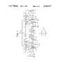
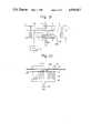
- FIG. 1is a schematic sectional view of a system for manufacturing a solar cell having a p-i-n structure in the roll-to-roll method in accordance with the present invention
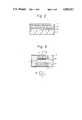
- FIG. 2is a sectional view of the solar cell manufactured by the system of FIG. 1;
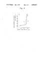
- FIG. 3is a view of a separator provided in the system of FIG. 1;
- FIG. 4illustrates a profile of boron in an i-type layer obtained by experiments
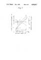
- FIG. 5is a perspective view of an example of a construction of the electrodes and separators
- FIG. 6is a sectional view of a reactor having a grid electrode between discharge electrodes
- FIG. 7illustrates the relationships of the deposition rate and energy conversion efficiency to the discharge power
- FIGS. 8 and 9are sectional views of reactors provided with separators and a grid electrode
- FIG. 10is a schematic view of a construction of discharge electrodes with a mask having an opening
- FIG. 11illustrates a mask having an opening without an electric-field-adjusting means
- FIG. 12illustrates a mask having an opening and provided with an electric-field-adjusting means
- FIG. 13shows a relationship of the conductivity of a deposited layer obtained in an experiment to the applied discharge power.
- FIG. 1illustrates a system for continuously manufacturing an amorphous silicon solar cell, as an example of the present invention.
- reaction chambers 1, 2 and 3are used for depositing p-type, i-type (intrinsic), and n-type amorphous silicon semiconductor layers.
- Reference numerals 4 to 9denote discharge electrodes
- reference numeral 10denotes a radio frequency power source for supplying a radio frequency power, typically 13, 56 MHz, to the discharge electrodes 4 to 9.
- silane (SiH 4 ) gasis fed from a gas inlet port 15 and decomposed at a given temperature in a plasma discharge atmosphere to deposit silicon onto the substrate 17.
- a p-type doping gase.g., diborane (B 2 H 6 )
- B 2 H 6diborane
- boronp-type dopant
- an n-type doping gase.g., phosphine (PH 3 ) is fed to form a silicon layer doped with phosphorus, an n-type dopant.
- a p-type amorphous silicon layer 31is transferred from a supply roll 20 in the supply roll chamber 18 to a take-up roll 21 in the take-up chamber 19, through the reaction chambers 1, 2 and 3, a p-type amorphous silicon layer 31, an i-type amorphous silicon layer 32, and an n-type amorphous silicon layer 33 are successively deposited on the substrate 17, thus forming a p-i-n layered structure of a solar cell (see FIG. 2).
- a mask 22is placed between the discharge electrodes 5 and 9 and the substrate 17 in the first and third reaction chambers 1 and 3 to control the layer thickness of the p-type and n-type silicon layers in this roll-to-roll method.
- control of a p-type dopant in an i-type silicon layeris preferably to attain a high efficiency of energy conversion of a solar cell, which should be done in the second reaction chamber 2.
- the problem of plasma damage of the interface between the i-type and underlying p-type silicon layersoccurs in the reaction chamber 2.
- the problem concerning the use of a mask to control the quality and layer thickness of a deposited layeroccurs in the first and third reaction chambers 1 and 3, when such a mask is used.
- separators 11are arranged between the discharge electrodes 6 and 7 in the second reaction chamber 2 to attain a desired profile of a dopant concentration in an i-type silicon layer.
- a grid electrode 23is preferably arranged between the discharge electrodes 6 and 7 only at a portion near the first reaction chamber 1, so that a high power can be applied to the discharge electrodes 6 and 7 to increase the deposition rate of silicon without causing plasma damage to the interface between the i-type and p-type silicon layers.
- An electric-field-adjusting meanssuch as a metal wire is provided for the mask 22 in the first and third reaction chambers 1 and 3, to make the electric field profile uniform in an opening of the mask 22.
- an amorphous silicon solar cell having an improved energy conversion efficiencycan be manufactured at a high deposition rate.
- FIG. 3is a sectional view of the reaction chamber 2 and illustrates the shape of the separator 11.
- the separator 11separated a space between the discharge electrodes 6 and 7 into a plurality of regions and acted as a barrier for the regions in all of the sections of the reaction chamber 2 except for slight gaps 14 between the separators 11 and the substrate 17 or the discharge electrodes 6 and 7.
- a reaction gas fed from an gas inlet port 15 at the downstream end, in the direction of movement of the substrate, of the reaction chamber 2must have passed through the gaps 14 to reach an outlet port 16 at the opposite upstream end of the reaction chamber 2.
- the separators 11were arranged at a slight distance from the respective discharge electrodes 6 and 7 to form gaps 14 therebetween.
- the gaps 14were formed to allow the passage of a reaction gas, to insulate the separators 11 from the power electrode 7, and to allow the passage of the substrate 17 near the electrically grounded electrode 6.
- the 14provided a distance of 3 mm between the separators 11 and the respective electrodes 6 and 7.
- the separators 11may be made of either an electrically conductive or insulating material but should be a material which does not release an impurity in the plasma. In this example, the separators 11 were made of stainless steel and were electrically grounded to the earth.
- the substrate 17was a 100 ⁇ m-thick polyethylene telephthalate film on which a 300 nm-thick aluminum layer and a 5 nm-thick stainless steel layer were laminated.
- a p-type amorphous silicon layer 31had been already deposited in the first reaction chamber 1 from a reaction gas of silane mixed with diboran (B 2 H 6 ) and the p-type silicon layer 31 had a thickness of 26 to 30 nm on the substrate 17.
- An n-type amorphous silicon layer 33 to be deposited in the third reaction chamber 3 from a reaction gas of silane mixed with phosphine (PH 3 ) and the n-type silicon layer 33would have the same thickness as that of the p-type silicon layer 31.
- An i-type or intrinsic amorphous silicon layer 32was deposited in the second reaction chamber 2 from silane gas without any doping gas and had a thickness of about 500 nm.
- the thickness of the layers 31 to 33 to be depositedwere different but the speed of movement of the substrate should be the same in the system in FIG. 1, the power output of the radio frequency power source, the size of the discharge electrodes, the amount of feed gas, the temperatures of the discharge electrodes, and the pressures in the reaction chambers, etc., were adjusted to attain the desired thicknesses of the layers deposited.
- the reaction gas of silanewas fed to the reaction chamber 2 from the gas inlet port 15 near the third reaction chamber 3 and evacuated from the gas outlet port 16 near the first reaction chamber 1.
- a solar cell having a p-i-n structurewas manufactured under the conditions described above, but a grid electrode 23 was not used in this example.
- the depth profile of boron atom of the thus-obtained solar cellwas examined by secondary ion mass spectroscopy (SIMS).
- SIMSsecondary ion mass spectroscopy
- the composition of the reaction gasmay be controlled such as having a distribution or profile in a reaction chamber from one end to another end thereof.
- a desired distribution of a reaction gascan be attained.
- FIG. 5illustrates a modification of a reaction chamber 2 in the system shown in FIG. 1.
- a reaction gasis fed through a discharge electrode 7' into respective separated regions between the discharge electrodes 6 and 7'.
- the electrode 7'has many pores 25 at the surface thereof, through which a reaction gas is fed to the respective regions, and contains a gas diffusing plate 26 by which the reaction gas fed from a gas inlet port 16' is distributed throughout the electrode 7'.
- FIG. 6shows a part of the reaction chamber 2' of the system of FIG. 1.
- the separators 11were not used and a discharge electrode 7' as shown in FIG. 5 was used in place of the discharge electrode 7 in FIG. 1.
- a grid electrode 23was arranged between the discharge electrodes 6 and 7'.
- the grid electrode 23was disposed along a substrate 17 and covered the full width of the substrate 17 and about one third of the length of the discharge electrodes 6 and 7' in the direction of movement of a substrate 17 from the end of the electrodes 6 and 7' where the substrate 17 was introduced.
- the grid electrode 23was capable of being supplied with a bias voltage (e.g., +200 V to -200 V) by a DC power source 12.
- the grid electrode 23was made of stainless steel and was a mesh having a mesh size of 200.
- the substrate 17was the same as that used in the former example.
- the structure of the layers of a solar cellwas also the same as in the former example. But the discharge power, the speed of movements of a substrate, and the pressure of the reaction gases, etc., were controlled to obtain the same structure of the layers.
- the grid electrode 23was spaced from the substrate 17 by a distance of 25 mm and the distance between the discharge electrodes 6 and 7' was 50 mm.
- the energy conversion efficiency of the solar cellwas not decreased although the discharge power or the deposition rate was increased.
- the energy conversion efficiency of the solar cellwas decreased with an increase of the discharge power or the deposition rate.
- the grid electrode covering the entire width and length of the discharge electrodethe deposition rate was not increased even if the discharge power was increased.
- FIGS. 8 and 9illustrate examples of a reactor for depositing a semiconductor layer, in which a combination of separators and a grid electrode described above is used.
- separators 11are arranged between the discharge electrodes 6 and 7' as in FIG. 1, i.e., throughout the space between the discharge electrodes 6 and 7' and a grid electrode 23 is arranged as in FIG. 6, i.e., between the discharge electrodes 6 and 7' only at a portion (one third) of the discharge electrodes 6 and 7' near the entrance of a substrate 17.
- the grid electrode 23overlaps some of the separators and generally should be electrically insulated from the separators, usually by spacing the grid electrode 23 from the separators 11.
- a grid electrode 23is arranged as in FIG. 6 and separators 11' are arranged only at the remaining portion of the space between the discharge electrodes, i.e., following the grid electrode 23 in the direction of movement of a substrate.
- FIG. 10shows an inner construction of a reactor used in the experiments, in which reference numeral 41 denotes an electrode which is electrically grounded, reference numeral 42 denotes a substrate of a polymer film which is continuously moved in the direction of the arrow, reference numeral 43 denotes a mask having an opening 43a (50 mm long and 250 mm wide) for controlling the thickness of a deposited layer, reference numeral 44 denotes a plasma, reference numeral 45 denotes a high frequency discharge electrode, and reference numeral 46 denotes a radio frequency power source for the electrodes 41 and 45, the frequency of the radio frequency discharge power being 13.56 MHz.
- an n-type amorphous silicon semiconductor layerwas deposited from a reaction gas of a mixture of hydrogen, silane and phosphine.
- the pressure in the reaction chamberwas 1 Torr
- the temperature of the substrate 42was 160° C.
- the discharge power appliedwas 0.05 W/cm 2
- the substrate 42was stopped for 30 minutes.
- the applied discharge powervaried from 0.01 to 0.04 W/cm 2 .
- the wirewas stainless steel and had a diameter of 1 mm.
- FIG. 13shows the conductivity of the resultant deposited silicon semiconductor layer at the center portion of the opening 43a.
- white circlesindicates a value measured under a light and black circles indicate a value measured in the dark. From these results, it was confirmed that even the central portion of the deposited silicon semiconductor layer was completely microcrystallized when a metal wire is provided at the mask opening. It was also confirmed that the deposited silicon semiconductor layer was a uniform microcrystalline film throughout the mask opening. As a result, the characteristics of the silicon semiconductor layer were desirably improved in comparison with those obtained in a conventional reactor.
- a deposited layercan be microcrystallized by a low power density, such as about 0.02 W/cm 2 , one half of a conventionally used power density. Note that distribution of the thickness obtained by this method were very uniform as compared with a conventional method, and thus no problem arose.
- a solar cell having a p-i-n structurecan be continuously manufactured on a flexible polymer film with an increased deposition rate without deterioration of the characteristics of a solar cell, but with an improved characteristic such as an energy conversion efficiency of a solar cell.
- the present inventionapparently may be also applied to a solar cell having an n-i-p structure, a p-i-n/p-i-n tandem structure or other structures, as well as any other multilayer semiconductor device. Note that the present invention is advantageous when a reactor is provided with any of separators and a grid electrode and, when the reactor includes a mask having an opening and an electric-field-adjusting means.
Landscapes
- Chemical & Material Sciences (AREA)
- Engineering & Computer Science (AREA)
- Physics & Mathematics (AREA)
- Plasma & Fusion (AREA)
- Analytical Chemistry (AREA)
- General Chemical & Material Sciences (AREA)
- Chemical Kinetics & Catalysis (AREA)
- Materials Engineering (AREA)
- Mechanical Engineering (AREA)
- Metallurgy (AREA)
- Organic Chemistry (AREA)
- Photovoltaic Devices (AREA)
Abstract
Description
TABLE ______________________________________ Value Invention Comparison (with (without Performance separators) separators) ______________________________________ Open circuit voltage 0.90 0.89 V.sub.OC [V] Short-circuit current 14.0 12.7 density [mA/cm.sup.2 ] Fill factor 0.71 0.65 Energy conversion 9.0 7.4 efficiency [%] ______________________________________
Claims (31)
Applications Claiming Priority (4)
| Application Number | Priority Date | Filing Date | Title |
|---|---|---|---|
| JP62061193AJPS63228676A (en) | 1987-03-18 | 1987-03-18 | Manufacture of thin film semiconductor device |
| JP62-61193 | 1987-03-18 | ||
| JP62-76384 | 1987-03-31 | ||
| JP62076384AJPS63244731A (en) | 1987-03-31 | 1987-03-31 | Plasma vapor growth device |
Publications (1)
| Publication Number | Publication Date |
|---|---|
| US4920917Atrue US4920917A (en) | 1990-05-01 |
Family
ID=26402235
Family Applications (1)
| Application Number | Title | Priority Date | Filing Date |
|---|---|---|---|
| US07/166,689Expired - LifetimeUS4920917A (en) | 1987-03-18 | 1988-03-11 | Reactor for depositing a layer on a moving substrate |
Country Status (3)
| Country | Link |
|---|---|
| US (1) | US4920917A (en) |
| DE (1) | DE3808974A1 (en) |
| FR (1) | FR2613535B1 (en) |
Cited By (69)
| Publication number | Priority date | Publication date | Assignee | Title |
|---|---|---|---|---|
| US5090356A (en)* | 1991-06-28 | 1992-02-25 | United Solar Systems Corporation | Chemically active isolation passageway for deposition chambers |
| US5224441A (en)* | 1991-09-27 | 1993-07-06 | The Boc Group, Inc. | Apparatus for rapid plasma treatments and method |
| US5378639A (en)* | 1992-07-24 | 1995-01-03 | Fuji Electric Co., Ltd. | Method for manufacturing a thin-film photovoltaic conversion device |
| US5393563A (en)* | 1991-10-29 | 1995-02-28 | Ellis, Jr.; Frank B. | Formation of tin oxide films on glass substrates |
| US5423971A (en)* | 1993-01-19 | 1995-06-13 | Leybold Aktiengesellschaft | Arrangement for coating substrates |
| US5468521A (en)* | 1991-10-28 | 1995-11-21 | Canon Kabushiki Kaisha | Method for forming a photoelectric deposited film |
| US5470784A (en)* | 1977-12-05 | 1995-11-28 | Plasma Physics Corp. | Method of forming semiconducting materials and barriers using a multiple chamber arrangement |
| US5547512A (en)* | 1989-07-21 | 1996-08-20 | Minnesota Mining And Manufacturing Company | Continuous atomspheric pressure CVD coating of fibers |
| US5578130A (en)* | 1990-12-12 | 1996-11-26 | Semiconductor Energy Laboratory Co., Ltd. | Apparatus and method for depositing a film |
| US5679167A (en)* | 1994-08-18 | 1997-10-21 | Sulzer Metco Ag | Plasma gun apparatus for forming dense, uniform coatings on large substrates |
| US5796116A (en)* | 1994-07-27 | 1998-08-18 | Sharp Kabushiki Kaisha | Thin-film semiconductor device including a semiconductor film with high field-effect mobility |
| US5879741A (en)* | 1993-03-24 | 1999-03-09 | Semiconductor Energy Laboratory Co., Ltd. | Apparatus and method for forming film |
| EP0828301A3 (en)* | 1996-09-05 | 1999-07-14 | Canon Kabushiki Kaisha | Photovoltaic element and method of and apparatus for manufacturing the same |
| EP0829910A3 (en)* | 1996-09-12 | 1999-08-11 | Canon Kabushiki Kaisha | Method and device for forming semiconductor thin films, and photovoltaic elements |
| US6001431A (en)* | 1992-12-28 | 1999-12-14 | Semiconductor Energy Laboratory Co., Ltd. | Process for fabricating a magnetic recording medium |
| US6001432A (en)* | 1992-11-19 | 1999-12-14 | Semiconductor Energy Laboratory Co., Ltd. | Apparatus for forming films on a substrate |
| US6168698B1 (en) | 1995-10-27 | 2001-01-02 | Balzers Und Leybold Deutschland Holding Ag | Apparatus for coating a substrate |
| US20020025389A1 (en)* | 2000-08-17 | 2002-02-28 | Yasuo Matsuzawa | Lens plasma coating system |
| KR100304766B1 (en)* | 1997-05-21 | 2002-03-08 | 가네꼬 히사시 | Silicon Oxide Film, Method of Forming the Same and Apparatus for Depositing the Same |
| US6490402B1 (en) | 2000-08-02 | 2002-12-03 | Sony Corporation | Flexible flat color display |
| AU756358B2 (en)* | 1996-09-05 | 2003-01-09 | Canon Kabushiki Kaisha | Photovoltaic element and method of and apparatus for manufacturing the same |
| US20030033982A1 (en)* | 2001-08-16 | 2003-02-20 | First Solar, Llc | Chemical vapor deposition system |
| US6564743B1 (en)* | 1996-05-27 | 2003-05-20 | Sony Corporation | Method for forming oxide film of semiconductor device, and oxide film forming apparatus capable of shortening pre-processing time for concentration measurement |
| US6620288B2 (en)* | 2000-03-22 | 2003-09-16 | Semiconductor Energy Laboratory Co., Ltd. | Substrate treatment apparatus |
| US6645573B2 (en)* | 1998-03-03 | 2003-11-11 | Canon Kabushiki Kaisha | Process for forming a microcrystalline silicon series thin film and apparatus suitable for practicing said process |
| US20040058199A1 (en)* | 2000-06-28 | 2004-03-25 | Mitsubishi Heavy Industries Ltd. | Hexagonal boron nitride film with low dielectric constant, layer dielectric film and method of production thereof, and plasma CVD apparatus |
| US7264850B1 (en) | 1992-12-28 | 2007-09-04 | Semiconductor Energy Laboratory Co., Ltd. | Process for treating a substrate with a plasma |
| US20090081441A1 (en)* | 2007-09-20 | 2009-03-26 | Lockheed Martin Corporation | Fiber Tow Comprising Carbon-Nanotube-Infused Fibers |
| US20090081383A1 (en)* | 2007-09-20 | 2009-03-26 | Lockheed Martin Corporation | Carbon Nanotube Infused Composites via Plasma Processing |
| US20100075455A1 (en)* | 2005-09-27 | 2010-03-25 | Semiconductor Energy Laboratory Co., Ltd. | Film formation apparatus, method for forming film, and method for manufacturing photoelectric conversion device |
| US20100159240A1 (en)* | 2007-01-03 | 2010-06-24 | Lockheed Martin Corporation | Cnt-infused metal fiber materials and process therefor |
| US20100178825A1 (en)* | 2007-01-03 | 2010-07-15 | Lockheed Martin Corporation | Cnt-infused carbon fiber materials and process therefor |
| US20100221424A1 (en)* | 2009-02-27 | 2010-09-02 | Lockheed Martin Corporation | Low temperature cnt growth using gas-preheat method |
| US20100227134A1 (en)* | 2009-03-03 | 2010-09-09 | Lockheed Martin Corporation | Method for the prevention of nanoparticle agglomeration at high temperatures |
| US20100260935A1 (en)* | 2009-04-09 | 2010-10-14 | Tokyo Electron Limited | Film deposition apparatus, film deposition method, and computer readable storage medium |
| US20100260933A1 (en)* | 2009-04-10 | 2010-10-14 | Lockheed Martin Corporation | Apparatus and method for the production of carbon nanotubes on a continuously moving substrate |
| US20100260998A1 (en)* | 2009-04-10 | 2010-10-14 | Lockheed Martin Corporation | Fiber sizing comprising nanoparticles |
| US20100271253A1 (en)* | 2009-04-24 | 2010-10-28 | Lockheed Martin Corporation | Cnt-based signature control material |
| US20100279569A1 (en)* | 2007-01-03 | 2010-11-04 | Lockheed Martin Corporation | Cnt-infused glass fiber materials and process therefor |
| US20100276072A1 (en)* | 2007-01-03 | 2010-11-04 | Lockheed Martin Corporation | CNT-Infused Fiber and Method Therefor |
| US20100279010A1 (en)* | 2009-04-30 | 2010-11-04 | Lockheed Martin Corporation | Method and system for close proximity catalysis for carbon nanotube synthesis |
| US20110028308A1 (en)* | 2009-08-03 | 2011-02-03 | Lockheed Martin Corporation | Incorporation of nanoparticles in composite fibers |
| US20110124483A1 (en)* | 2009-11-23 | 2011-05-26 | Applied Nanostructured Solutions, Llc | Ceramic composite materials containing carbon nanotube-infused fiber materials and methods for production thereof |
| US20110132245A1 (en)* | 2009-11-23 | 2011-06-09 | Applied Nanostructured Solutions, Llc | Cnt-tailored composite sea-based structures |
| US20110143019A1 (en)* | 2009-12-14 | 2011-06-16 | Amprius, Inc. | Apparatus for Deposition on Two Sides of the Web |
| US20110171469A1 (en)* | 2009-11-02 | 2011-07-14 | Applied Nanostructured Solutions, Llc | Cnt-infused aramid fiber materials and process therefor |
| US20110168083A1 (en)* | 2007-01-03 | 2011-07-14 | Lockheed Martin Corporation | Cnt-infused ceramic fiber materials and process therefor |
| CN102244152A (en)* | 2010-05-12 | 2011-11-16 | 吉林庆达新能源电力股份有限公司 | Method for depositing amorphous silicon thin film in production of solar cells |
| US8545963B2 (en) | 2009-12-14 | 2013-10-01 | Applied Nanostructured Solutions, Llc | Flame-resistant composite materials and articles containing carbon nanotube-infused fiber materials |
| US8585934B2 (en) | 2009-02-17 | 2013-11-19 | Applied Nanostructured Solutions, Llc | Composites comprising carbon nanotubes on fiber |
| US8665581B2 (en) | 2010-03-02 | 2014-03-04 | Applied Nanostructured Solutions, Llc | Spiral wound electrical devices containing carbon nanotube-infused electrode materials and methods and apparatuses for production thereof |
| US8664573B2 (en) | 2009-04-27 | 2014-03-04 | Applied Nanostructured Solutions, Llc | CNT-based resistive heating for deicing composite structures |
| US8780526B2 (en) | 2010-06-15 | 2014-07-15 | Applied Nanostructured Solutions, Llc | Electrical devices containing carbon nanotube-infused fibers and methods for production thereof |
| US8784937B2 (en) | 2010-09-14 | 2014-07-22 | Applied Nanostructured Solutions, Llc | Glass substrates having carbon nanotubes grown thereon and methods for production thereof |
| US8787001B2 (en) | 2010-03-02 | 2014-07-22 | Applied Nanostructured Solutions, Llc | Electrical devices containing carbon nanotube-infused fibers and methods for production thereof |
| US8815341B2 (en) | 2010-09-22 | 2014-08-26 | Applied Nanostructured Solutions, Llc | Carbon fiber substrates having carbon nanotubes grown thereon and processes for production thereof |
| US8999453B2 (en) | 2010-02-02 | 2015-04-07 | Applied Nanostructured Solutions, Llc | Carbon nanotube-infused fiber materials containing parallel-aligned carbon nanotubes, methods for production thereof, and composite materials derived therefrom |
| US9005755B2 (en) | 2007-01-03 | 2015-04-14 | Applied Nanostructured Solutions, Llc | CNS-infused carbon nanomaterials and process therefor |
| US9017854B2 (en) | 2010-08-30 | 2015-04-28 | Applied Nanostructured Solutions, Llc | Structural energy storage assemblies and methods for production thereof |
| US9085464B2 (en) | 2012-03-07 | 2015-07-21 | Applied Nanostructured Solutions, Llc | Resistance measurement system and method of using the same |
| US9111658B2 (en) | 2009-04-24 | 2015-08-18 | Applied Nanostructured Solutions, Llc | CNS-shielded wires |
| US9163354B2 (en) | 2010-01-15 | 2015-10-20 | Applied Nanostructured Solutions, Llc | CNT-infused fiber as a self shielding wire for enhanced power transmission line |
| US9167736B2 (en) | 2010-01-15 | 2015-10-20 | Applied Nanostructured Solutions, Llc | CNT-infused fiber as a self shielding wire for enhanced power transmission line |
| US20160002785A1 (en)* | 2013-02-28 | 2016-01-07 | Mitsui Engineering & Shipbuilding Co., Ltd. | Layer-forming device and layer-forming method |
| US20180174800A1 (en)* | 2016-12-15 | 2018-06-21 | Toyota Jidosha Kabushiki Kaisha | Plasma device |
| US20190112708A1 (en)* | 2014-02-11 | 2019-04-18 | Kenneth Scott Alexander Butcher | Electrostatic control of metal wetting layers during deposition |
| US20200083452A1 (en)* | 2017-02-24 | 2020-03-12 | Applied Materials, Inc. | Apparatus for vacuum processing of a substrate, system for vacuum processing of a substrate, and method for transportation of a substrate carrier and a mask carrier in a vacuum chamber |
| US11315767B2 (en) | 2017-09-25 | 2022-04-26 | Toyota Jidosha Kabushiki Kaisha | Plasma processing apparatus |
| CN114622183A (en)* | 2020-12-11 | 2022-06-14 | 湖南红太阳光电科技有限公司 | Method for preparing silicon oxide film |
Families Citing this family (3)
| Publication number | Priority date | Publication date | Assignee | Title |
|---|---|---|---|---|
| DE19500964A1 (en)* | 1995-01-14 | 1996-07-18 | Leybold Ag | Cathode sputtering appts. for coating flat substrates, esp. optical components |
| DE19540255A1 (en)* | 1995-10-28 | 1997-04-30 | Leybold Ag | Apparatus for film coating a substrate |
| DE19540053A1 (en)* | 1995-10-27 | 1997-04-30 | Leybold Ag | Substrate coating device for application of non-conductive layers using magnetron sputtering |
Citations (3)
| Publication number | Priority date | Publication date | Assignee | Title |
|---|---|---|---|---|
| JPS55125681A (en)* | 1979-03-22 | 1980-09-27 | Sanyo Electric Co Ltd | Manufacture of photovoltaic device |
| US4438723A (en)* | 1981-09-28 | 1984-03-27 | Energy Conversion Devices, Inc. | Multiple chamber deposition and isolation system and method |
| US4450787A (en)* | 1982-06-03 | 1984-05-29 | Rca Corporation | Glow discharge plasma deposition of thin films |
Family Cites Families (6)
| Publication number | Priority date | Publication date | Assignee | Title |
|---|---|---|---|---|
| JPS5694749A (en)* | 1979-12-28 | 1981-07-31 | Matsushita Electronics Corp | Plasma heaping device |
| DE3272239D1 (en)* | 1981-03-16 | 1986-09-04 | Energy Conversion Devices Inc | Apparatus including improved cathode for continuous deposition of amorphous material |
| US4492181A (en)* | 1982-03-19 | 1985-01-08 | Sovonics Solar Systems | Apparatus for continuously producing tandem amorphous photovoltaic cells |
| US4423701A (en)* | 1982-03-29 | 1984-01-03 | Energy Conversion Devices, Inc. | Glow discharge deposition apparatus including a non-horizontally disposed cathode |
| US4438724A (en)* | 1982-08-13 | 1984-03-27 | Energy Conversion Devices, Inc. | Grooved gas gate |
| US4608943A (en)* | 1984-10-24 | 1986-09-02 | Sovonics Solar Systems | Cathode assembly with localized profiling capabilities |
- 1988
- 1988-03-11USUS07/166,689patent/US4920917A/ennot_activeExpired - Lifetime
- 1988-03-17DEDE3808974Apatent/DE3808974A1/enactiveGranted
- 1988-03-18FRFR8803589Apatent/FR2613535B1/ennot_activeExpired - Fee Related
Patent Citations (3)
| Publication number | Priority date | Publication date | Assignee | Title |
|---|---|---|---|---|
| JPS55125681A (en)* | 1979-03-22 | 1980-09-27 | Sanyo Electric Co Ltd | Manufacture of photovoltaic device |
| US4438723A (en)* | 1981-09-28 | 1984-03-27 | Energy Conversion Devices, Inc. | Multiple chamber deposition and isolation system and method |
| US4450787A (en)* | 1982-06-03 | 1984-05-29 | Rca Corporation | Glow discharge plasma deposition of thin films |
Non-Patent Citations (2)
| Title |
|---|
| Technical Digest P I 16 1st Photovoltaic Science and Engineering Conference Nov. 13 16/1984 pp. 187 190.* |
| Technical Digest P-I-16 1st Photovoltaic Science and Engineering Conference Nov. 13-16/1984 pp. 187-190. |
Cited By (110)
| Publication number | Priority date | Publication date | Assignee | Title |
|---|---|---|---|---|
| US5470784A (en)* | 1977-12-05 | 1995-11-28 | Plasma Physics Corp. | Method of forming semiconducting materials and barriers using a multiple chamber arrangement |
| US5547512A (en)* | 1989-07-21 | 1996-08-20 | Minnesota Mining And Manufacturing Company | Continuous atomspheric pressure CVD coating of fibers |
| US5578130A (en)* | 1990-12-12 | 1996-11-26 | Semiconductor Energy Laboratory Co., Ltd. | Apparatus and method for depositing a film |
| WO1993000455A1 (en)* | 1991-06-28 | 1993-01-07 | United Solar Systems Corporation | Chemically active isolation passageway for deposition chambers |
| US5090356A (en)* | 1991-06-28 | 1992-02-25 | United Solar Systems Corporation | Chemically active isolation passageway for deposition chambers |
| US5224441A (en)* | 1991-09-27 | 1993-07-06 | The Boc Group, Inc. | Apparatus for rapid plasma treatments and method |
| US5364665A (en)* | 1991-09-27 | 1994-11-15 | The Boc Group, Inc. | Method for rapid plasma treatments |
| US5468521A (en)* | 1991-10-28 | 1995-11-21 | Canon Kabushiki Kaisha | Method for forming a photoelectric deposited film |
| US5393563A (en)* | 1991-10-29 | 1995-02-28 | Ellis, Jr.; Frank B. | Formation of tin oxide films on glass substrates |
| US5487784A (en)* | 1991-10-29 | 1996-01-30 | Ellis, Jr.; Frank B. | Formation of tin oxide films on glass substrates |
| US5378639A (en)* | 1992-07-24 | 1995-01-03 | Fuji Electric Co., Ltd. | Method for manufacturing a thin-film photovoltaic conversion device |
| US6001432A (en)* | 1992-11-19 | 1999-12-14 | Semiconductor Energy Laboratory Co., Ltd. | Apparatus for forming films on a substrate |
| US6001431A (en)* | 1992-12-28 | 1999-12-14 | Semiconductor Energy Laboratory Co., Ltd. | Process for fabricating a magnetic recording medium |
| US7264850B1 (en) | 1992-12-28 | 2007-09-04 | Semiconductor Energy Laboratory Co., Ltd. | Process for treating a substrate with a plasma |
| US5423971A (en)* | 1993-01-19 | 1995-06-13 | Leybold Aktiengesellschaft | Arrangement for coating substrates |
| US6261634B1 (en) | 1993-03-24 | 2001-07-17 | Semiconductor Energy Laboratory Co., Ltd. | Apparatus and method for forming film |
| US5879741A (en)* | 1993-03-24 | 1999-03-09 | Semiconductor Energy Laboratory Co., Ltd. | Apparatus and method for forming film |
| US6271062B1 (en) | 1994-07-27 | 2001-08-07 | Sharp Kabushiki Kaisha | Thin film semiconductor device including a semiconductor film with high field-effect mobility |
| US5796116A (en)* | 1994-07-27 | 1998-08-18 | Sharp Kabushiki Kaisha | Thin-film semiconductor device including a semiconductor film with high field-effect mobility |
| US5853815A (en)* | 1994-08-18 | 1998-12-29 | Sulzer Metco Ag | Method of forming uniform thin coatings on large substrates |
| US5679167A (en)* | 1994-08-18 | 1997-10-21 | Sulzer Metco Ag | Plasma gun apparatus for forming dense, uniform coatings on large substrates |
| US6168698B1 (en) | 1995-10-27 | 2001-01-02 | Balzers Und Leybold Deutschland Holding Ag | Apparatus for coating a substrate |
| US6564743B1 (en)* | 1996-05-27 | 2003-05-20 | Sony Corporation | Method for forming oxide film of semiconductor device, and oxide film forming apparatus capable of shortening pre-processing time for concentration measurement |
| US20050161077A1 (en)* | 1996-09-05 | 2005-07-28 | Canon Kabushiki Kaisha | Apparatus for manufacturing photovoltaic elements |
| AU756358B2 (en)* | 1996-09-05 | 2003-01-09 | Canon Kabushiki Kaisha | Photovoltaic element and method of and apparatus for manufacturing the same |
| EP0828301A3 (en)* | 1996-09-05 | 1999-07-14 | Canon Kabushiki Kaisha | Photovoltaic element and method of and apparatus for manufacturing the same |
| US6162988A (en)* | 1996-09-05 | 2000-12-19 | Canon Kabushiki Kaisha | Photovoltaic element |
| US6368944B1 (en) | 1996-09-05 | 2002-04-09 | Canon Kabushiki Kaisha | Method of manufacturing photovoltaic element and apparatus therefor |
| AU745938B2 (en)* | 1996-09-05 | 2002-04-11 | Canon Kabushiki Kaisha | Photovoltaic element and method of and apparatus for manufacturing the same |
| US6159763A (en)* | 1996-09-12 | 2000-12-12 | Canon Kabushiki Kaisha | Method and device for forming semiconductor thin film, and method and device for forming photovoltaic element |
| EP0829910A3 (en)* | 1996-09-12 | 1999-08-11 | Canon Kabushiki Kaisha | Method and device for forming semiconductor thin films, and photovoltaic elements |
| US6444327B1 (en) | 1997-05-21 | 2002-09-03 | Nec Corporation | Silicon oxide film, method of forming the silicon oxide film, and apparatus for depositing the silicon oxide film |
| US6383299B1 (en) | 1997-05-21 | 2002-05-07 | Nec Corporation | Silicon oxide film, method of forming the silicon oxide film, and apparatus for depositing the silicon oxide film |
| KR100304766B1 (en)* | 1997-05-21 | 2002-03-08 | 가네꼬 히사시 | Silicon Oxide Film, Method of Forming the Same and Apparatus for Depositing the Same |
| US6830786B2 (en) | 1997-05-21 | 2004-12-14 | Nec Corporation | Silicon oxide film, method of forming the silicon oxide film, and apparatus for depositing the silicon oxide film |
| US20040045505A1 (en)* | 1998-03-03 | 2004-03-11 | Makoto Higashikawa | Process for forming a microcrystalline silicon series thin film and apparatus suitable for practicing said process |
| US6645573B2 (en)* | 1998-03-03 | 2003-11-11 | Canon Kabushiki Kaisha | Process for forming a microcrystalline silicon series thin film and apparatus suitable for practicing said process |
| US6620288B2 (en)* | 2000-03-22 | 2003-09-16 | Semiconductor Energy Laboratory Co., Ltd. | Substrate treatment apparatus |
| US20040058199A1 (en)* | 2000-06-28 | 2004-03-25 | Mitsubishi Heavy Industries Ltd. | Hexagonal boron nitride film with low dielectric constant, layer dielectric film and method of production thereof, and plasma CVD apparatus |
| US6490402B1 (en) | 2000-08-02 | 2002-12-03 | Sony Corporation | Flexible flat color display |
| US20020025389A1 (en)* | 2000-08-17 | 2002-02-28 | Yasuo Matsuzawa | Lens plasma coating system |
| US6881269B2 (en)* | 2000-08-17 | 2005-04-19 | Novartis Ag | Lens plasma coating system |
| US6719848B2 (en)* | 2001-08-16 | 2004-04-13 | First Solar, Llc | Chemical vapor deposition system |
| US20030033982A1 (en)* | 2001-08-16 | 2003-02-20 | First Solar, Llc | Chemical vapor deposition system |
| US20110232571A1 (en)* | 2005-09-27 | 2011-09-29 | Semiconductor Energy Laboratory Co., Ltd. | Film formation apparatus, method for forming film, and method for manufacturing photoelectric conversion device |
| US8192545B2 (en) | 2005-09-27 | 2012-06-05 | Semiconductor Energy Laboratory Co., Ltd. | Film formation apparatus, method for forming film, and method for manufacturing photoelectric conversion device |
| US20100075455A1 (en)* | 2005-09-27 | 2010-03-25 | Semiconductor Energy Laboratory Co., Ltd. | Film formation apparatus, method for forming film, and method for manufacturing photoelectric conversion device |
| US7985664B2 (en)* | 2005-09-27 | 2011-07-26 | Semiconductor Energy Laboratory Co., Ltd. | Film formation apparatus, method for forming film, and method for manufacturing photoelectric conversion device |
| US20110168083A1 (en)* | 2007-01-03 | 2011-07-14 | Lockheed Martin Corporation | Cnt-infused ceramic fiber materials and process therefor |
| US20100178825A1 (en)* | 2007-01-03 | 2010-07-15 | Lockheed Martin Corporation | Cnt-infused carbon fiber materials and process therefor |
| US20100159240A1 (en)* | 2007-01-03 | 2010-06-24 | Lockheed Martin Corporation | Cnt-infused metal fiber materials and process therefor |
| US8158217B2 (en) | 2007-01-03 | 2012-04-17 | Applied Nanostructured Solutions, Llc | CNT-infused fiber and method therefor |
| US20110168089A1 (en)* | 2007-01-03 | 2011-07-14 | Lockheed Martin Corporation | Cnt-infused carbon fiber materials and process therefor |
| US8951632B2 (en) | 2007-01-03 | 2015-02-10 | Applied Nanostructured Solutions, Llc | CNT-infused carbon fiber materials and process therefor |
| US9574300B2 (en) | 2007-01-03 | 2017-02-21 | Applied Nanostructured Solutions, Llc | CNT-infused carbon fiber materials and process therefor |
| US20100279569A1 (en)* | 2007-01-03 | 2010-11-04 | Lockheed Martin Corporation | Cnt-infused glass fiber materials and process therefor |
| US20100276072A1 (en)* | 2007-01-03 | 2010-11-04 | Lockheed Martin Corporation | CNT-Infused Fiber and Method Therefor |
| US9573812B2 (en) | 2007-01-03 | 2017-02-21 | Applied Nanostructured Solutions, Llc | CNT-infused metal fiber materials and process therefor |
| US9005755B2 (en) | 2007-01-03 | 2015-04-14 | Applied Nanostructured Solutions, Llc | CNS-infused carbon nanomaterials and process therefor |
| US8951631B2 (en) | 2007-01-03 | 2015-02-10 | Applied Nanostructured Solutions, Llc | CNT-infused metal fiber materials and process therefor |
| US20090081383A1 (en)* | 2007-09-20 | 2009-03-26 | Lockheed Martin Corporation | Carbon Nanotube Infused Composites via Plasma Processing |
| US20090081441A1 (en)* | 2007-09-20 | 2009-03-26 | Lockheed Martin Corporation | Fiber Tow Comprising Carbon-Nanotube-Infused Fibers |
| US8585934B2 (en) | 2009-02-17 | 2013-11-19 | Applied Nanostructured Solutions, Llc | Composites comprising carbon nanotubes on fiber |
| US20100221424A1 (en)* | 2009-02-27 | 2010-09-02 | Lockheed Martin Corporation | Low temperature cnt growth using gas-preheat method |
| US8580342B2 (en) | 2009-02-27 | 2013-11-12 | Applied Nanostructured Solutions, Llc | Low temperature CNT growth using gas-preheat method |
| US10138128B2 (en) | 2009-03-03 | 2018-11-27 | Applied Nanostructured Solutions, Llc | System and method for surface treatment and barrier coating of fibers for in situ CNT growth |
| US20100227134A1 (en)* | 2009-03-03 | 2010-09-09 | Lockheed Martin Corporation | Method for the prevention of nanoparticle agglomeration at high temperatures |
| US8882915B2 (en)* | 2009-04-09 | 2014-11-11 | Tokyo Electron Limited | Film deposition apparatus, film deposition method, and computer readable storage medium |
| US20100260935A1 (en)* | 2009-04-09 | 2010-10-14 | Tokyo Electron Limited | Film deposition apparatus, film deposition method, and computer readable storage medium |
| US20100260998A1 (en)* | 2009-04-10 | 2010-10-14 | Lockheed Martin Corporation | Fiber sizing comprising nanoparticles |
| US20100260933A1 (en)* | 2009-04-10 | 2010-10-14 | Lockheed Martin Corporation | Apparatus and method for the production of carbon nanotubes on a continuously moving substrate |
| US9111658B2 (en) | 2009-04-24 | 2015-08-18 | Applied Nanostructured Solutions, Llc | CNS-shielded wires |
| US8325079B2 (en) | 2009-04-24 | 2012-12-04 | Applied Nanostructured Solutions, Llc | CNT-based signature control material |
| US9241433B2 (en) | 2009-04-24 | 2016-01-19 | Applied Nanostructured Solutions, Llc | CNT-infused EMI shielding composite and coating |
| US20100271253A1 (en)* | 2009-04-24 | 2010-10-28 | Lockheed Martin Corporation | Cnt-based signature control material |
| US8664573B2 (en) | 2009-04-27 | 2014-03-04 | Applied Nanostructured Solutions, Llc | CNT-based resistive heating for deicing composite structures |
| US20100279010A1 (en)* | 2009-04-30 | 2010-11-04 | Lockheed Martin Corporation | Method and system for close proximity catalysis for carbon nanotube synthesis |
| US20110028308A1 (en)* | 2009-08-03 | 2011-02-03 | Lockheed Martin Corporation | Incorporation of nanoparticles in composite fibers |
| US8969225B2 (en) | 2009-08-03 | 2015-03-03 | Applied Nano Structured Soultions, LLC | Incorporation of nanoparticles in composite fibers |
| US20110171469A1 (en)* | 2009-11-02 | 2011-07-14 | Applied Nanostructured Solutions, Llc | Cnt-infused aramid fiber materials and process therefor |
| US20110132245A1 (en)* | 2009-11-23 | 2011-06-09 | Applied Nanostructured Solutions, Llc | Cnt-tailored composite sea-based structures |
| US8662449B2 (en) | 2009-11-23 | 2014-03-04 | Applied Nanostructured Solutions, Llc | CNT-tailored composite air-based structures |
| US20110124483A1 (en)* | 2009-11-23 | 2011-05-26 | Applied Nanostructured Solutions, Llc | Ceramic composite materials containing carbon nanotube-infused fiber materials and methods for production thereof |
| US8601965B2 (en) | 2009-11-23 | 2013-12-10 | Applied Nanostructured Solutions, Llc | CNT-tailored composite sea-based structures |
| US8168291B2 (en) | 2009-11-23 | 2012-05-01 | Applied Nanostructured Solutions, Llc | Ceramic composite materials containing carbon nanotube-infused fiber materials and methods for production thereof |
| US11695125B2 (en) | 2009-12-14 | 2023-07-04 | Amprius Technologies, Inc. | Deposition on two sides of a web |
| US20110143019A1 (en)* | 2009-12-14 | 2011-06-16 | Amprius, Inc. | Apparatus for Deposition on Two Sides of the Web |
| US10044046B2 (en)* | 2009-12-14 | 2018-08-07 | Amprius, Inc. | Deposition on two sides of a web |
| US8545963B2 (en) | 2009-12-14 | 2013-10-01 | Applied Nanostructured Solutions, Llc | Flame-resistant composite materials and articles containing carbon nanotube-infused fiber materials |
| US9163354B2 (en) | 2010-01-15 | 2015-10-20 | Applied Nanostructured Solutions, Llc | CNT-infused fiber as a self shielding wire for enhanced power transmission line |
| US9167736B2 (en) | 2010-01-15 | 2015-10-20 | Applied Nanostructured Solutions, Llc | CNT-infused fiber as a self shielding wire for enhanced power transmission line |
| US8999453B2 (en) | 2010-02-02 | 2015-04-07 | Applied Nanostructured Solutions, Llc | Carbon nanotube-infused fiber materials containing parallel-aligned carbon nanotubes, methods for production thereof, and composite materials derived therefrom |
| US8787001B2 (en) | 2010-03-02 | 2014-07-22 | Applied Nanostructured Solutions, Llc | Electrical devices containing carbon nanotube-infused fibers and methods for production thereof |
| US8665581B2 (en) | 2010-03-02 | 2014-03-04 | Applied Nanostructured Solutions, Llc | Spiral wound electrical devices containing carbon nanotube-infused electrode materials and methods and apparatuses for production thereof |
| CN102244152A (en)* | 2010-05-12 | 2011-11-16 | 吉林庆达新能源电力股份有限公司 | Method for depositing amorphous silicon thin film in production of solar cells |
| CN102244152B (en)* | 2010-05-12 | 2013-09-04 | 吉林庆达新能源电力股份有限公司 | Method for depositing amorphous silicon thin film in production of solar cells |
| US8780526B2 (en) | 2010-06-15 | 2014-07-15 | Applied Nanostructured Solutions, Llc | Electrical devices containing carbon nanotube-infused fibers and methods for production thereof |
| US9017854B2 (en) | 2010-08-30 | 2015-04-28 | Applied Nanostructured Solutions, Llc | Structural energy storage assemblies and methods for production thereof |
| US9907174B2 (en) | 2010-08-30 | 2018-02-27 | Applied Nanostructured Solutions, Llc | Structural energy storage assemblies and methods for production thereof |
| US8784937B2 (en) | 2010-09-14 | 2014-07-22 | Applied Nanostructured Solutions, Llc | Glass substrates having carbon nanotubes grown thereon and methods for production thereof |
| US8815341B2 (en) | 2010-09-22 | 2014-08-26 | Applied Nanostructured Solutions, Llc | Carbon fiber substrates having carbon nanotubes grown thereon and processes for production thereof |
| US9085464B2 (en) | 2012-03-07 | 2015-07-21 | Applied Nanostructured Solutions, Llc | Resistance measurement system and method of using the same |
| US20160002785A1 (en)* | 2013-02-28 | 2016-01-07 | Mitsui Engineering & Shipbuilding Co., Ltd. | Layer-forming device and layer-forming method |
| US10246776B2 (en)* | 2013-02-28 | 2019-04-02 | Mitsui E&S Machinery Co., Ltd | Layer-forming device and layer-forming method |
| US20190112708A1 (en)* | 2014-02-11 | 2019-04-18 | Kenneth Scott Alexander Butcher | Electrostatic control of metal wetting layers during deposition |
| US20180174800A1 (en)* | 2016-12-15 | 2018-06-21 | Toyota Jidosha Kabushiki Kaisha | Plasma device |
| US11251019B2 (en)* | 2016-12-15 | 2022-02-15 | Toyota Jidosha Kabushiki Kaisha | Plasma device |
| US20200083452A1 (en)* | 2017-02-24 | 2020-03-12 | Applied Materials, Inc. | Apparatus for vacuum processing of a substrate, system for vacuum processing of a substrate, and method for transportation of a substrate carrier and a mask carrier in a vacuum chamber |
| US11315767B2 (en) | 2017-09-25 | 2022-04-26 | Toyota Jidosha Kabushiki Kaisha | Plasma processing apparatus |
| CN114622183A (en)* | 2020-12-11 | 2022-06-14 | 湖南红太阳光电科技有限公司 | Method for preparing silicon oxide film |
Also Published As
| Publication number | Publication date |
|---|---|
| DE3808974C2 (en) | 1991-04-18 |
| FR2613535A1 (en) | 1988-10-07 |
| DE3808974A1 (en) | 1988-09-29 |
| FR2613535B1 (en) | 1996-01-12 |
Similar Documents
| Publication | Publication Date | Title |
|---|---|---|
| US4920917A (en) | Reactor for depositing a layer on a moving substrate | |
| US6100465A (en) | Solar battery having a plurality of I-type layers with different hydrogen densities | |
| US5927994A (en) | Method for manufacturing thin film | |
| US7030313B2 (en) | Thin film solar cell and method of manufacturing the same | |
| US7238545B2 (en) | Method for fabricating tandem thin film photoelectric converter | |
| US6268235B1 (en) | Method for manufacturing a photoelectric conversion device | |
| JP3437386B2 (en) | Photovoltaic element and manufacturing method thereof | |
| EP0829910A2 (en) | Method and device for forming semiconductor thin films, and photovoltaic elements | |
| US4462333A (en) | Process gas introduction, confinement and evacuation system for glow discharge deposition apparatus | |
| EP0179569B1 (en) | Improved cathode for glow discharge deposition apparatus | |
| US6057005A (en) | Method of forming semiconductor thin film | |
| EP0109148A2 (en) | Substrate shield for preventing the deposition of nonhomogeneous films | |
| US20060219170A1 (en) | Pore cathode for the mass production of photovoltaic devices having increased conversion efficiency | |
| JPH10209479A (en) | Apparatus for producing semiconductor thin film and photovoltaic element | |
| US20040250763A1 (en) | Fountain cathode for large area plasma deposition | |
| JPH0227775A (en) | Manufacture of solar cell | |
| JP3403039B2 (en) | Apparatus and method for manufacturing thin film semiconductor by plasma CVD method | |
| JP3554314B2 (en) | Deposition film formation method | |
| JPH10229213A (en) | Method of forming semiconductor thin film | |
| JPS62262419A (en) | Plasma CVD equipment | |
| JP3690772B2 (en) | Photovoltaic element forming apparatus and forming method | |
| JPH0365653B2 (en) | ||
| JP3403001B2 (en) | Apparatus and method for manufacturing thin film semiconductor by plasma CVD method | |
| EP0087479A1 (en) | Method and device producing amorphous silicon solar battery | |
| JP3403038B2 (en) | Apparatus and method for manufacturing thin film semiconductor by plasma CVD method |
Legal Events
| Date | Code | Title | Description |
|---|---|---|---|
| AS | Assignment | Owner name:TEIJIN LIMITED, 11, MINAMIHONMACHI 1-CHOME, HIGASH Free format text:ASSIGNMENT OF ASSIGNORS INTEREST.;ASSIGNORS:NAKATANI, KENJI;OKANIWA, HIROSHI;YANO, MITSUAKI;REEL/FRAME:004857/0702 Effective date:19880301 Owner name:TEIJIN LIMITED, JAPAN Free format text:ASSIGNMENT OF ASSIGNORS INTEREST;ASSIGNORS:NAKATANI, KENJI;OKANIWA, HIROSHI;YANO, MITSUAKI;REEL/FRAME:004857/0702 Effective date:19880301 | |
| STCF | Information on status: patent grant | Free format text:PATENTED CASE | |
| FEPP | Fee payment procedure | Free format text:PAYOR NUMBER ASSIGNED (ORIGINAL EVENT CODE: ASPN); ENTITY STATUS OF PATENT OWNER: LARGE ENTITY | |
| CC | Certificate of correction | ||
| FPAY | Fee payment | Year of fee payment:4 | |
| AS | Assignment | Owner name:NEW ENERGY AND INDUSTRIAL TECHNOLOGY DEVELOPMENT O Free format text:ASSIGNMENT OF ASSIGNORS INTEREST;ASSIGNOR:TEIJIN LIMITED;REEL/FRAME:008313/0696 Effective date:19961127 | |
| FPAY | Fee payment | Year of fee payment:8 | |
| FPAY | Fee payment | Year of fee payment:12 |