US4920073A - Selective silicidation process using a titanium nitride protective layer - Google Patents
Selective silicidation process using a titanium nitride protective layerDownload PDFInfo
- Publication number
- US4920073A US4920073AUS07/350,429US35042989AUS4920073AUS 4920073 AUS4920073 AUS 4920073AUS 35042989 AUS35042989 AUS 35042989AUS 4920073 AUS4920073 AUS 4920073A
- Authority
- US
- United States
- Prior art keywords
- titanium
- layer
- integrated circuit
- titanium nitride
- silicon
- Prior art date
- Legal status (The legal status is an assumption and is not a legal conclusion. Google has not performed a legal analysis and makes no representation as to the accuracy of the status listed.)
- Expired - Lifetime
Links
Images

Classifications
- H—ELECTRICITY
- H10—SEMICONDUCTOR DEVICES; ELECTRIC SOLID-STATE DEVICES NOT OTHERWISE PROVIDED FOR
- H10D—INORGANIC ELECTRIC SEMICONDUCTOR DEVICES
- H10D30/00—Field-effect transistors [FET]
- H10D30/01—Manufacture or treatment
- H10D30/021—Manufacture or treatment of FETs having insulated gates [IGFET]
- H10D30/0212—Manufacture or treatment of FETs having insulated gates [IGFET] using self-aligned silicidation
- H—ELECTRICITY
- H01—ELECTRIC ELEMENTS
- H01L—SEMICONDUCTOR DEVICES NOT COVERED BY CLASS H10
- H01L21/00—Processes or apparatus adapted for the manufacture or treatment of semiconductor or solid state devices or of parts thereof
- H01L21/02—Manufacture or treatment of semiconductor devices or of parts thereof
- H01L21/04—Manufacture or treatment of semiconductor devices or of parts thereof the devices having potential barriers, e.g. a PN junction, depletion layer or carrier concentration layer
- H01L21/18—Manufacture or treatment of semiconductor devices or of parts thereof the devices having potential barriers, e.g. a PN junction, depletion layer or carrier concentration layer the devices having semiconductor bodies comprising elements of Group IV of the Periodic Table or AIIIBV compounds with or without impurities, e.g. doping materials
- H01L21/30—Treatment of semiconductor bodies using processes or apparatus not provided for in groups H01L21/20 - H01L21/26
- H01L21/31—Treatment of semiconductor bodies using processes or apparatus not provided for in groups H01L21/20 - H01L21/26 to form insulating layers thereon, e.g. for masking or by using photolithographic techniques; After treatment of these layers; Selection of materials for these layers
- H01L21/3205—Deposition of non-insulating-, e.g. conductive- or resistive-, layers on insulating layers; After-treatment of these layers
- H01L21/321—After treatment
- H01L21/3211—Nitridation of silicon-containing layers
- Y—GENERAL TAGGING OF NEW TECHNOLOGICAL DEVELOPMENTS; GENERAL TAGGING OF CROSS-SECTIONAL TECHNOLOGIES SPANNING OVER SEVERAL SECTIONS OF THE IPC; TECHNICAL SUBJECTS COVERED BY FORMER USPC CROSS-REFERENCE ART COLLECTIONS [XRACs] AND DIGESTS
- Y10—TECHNICAL SUBJECTS COVERED BY FORMER USPC
- Y10S—TECHNICAL SUBJECTS COVERED BY FORMER USPC CROSS-REFERENCE ART COLLECTIONS [XRACs] AND DIGESTS
- Y10S148/00—Metal treatment
- Y10S148/113—Nitrides of boron or aluminum or gallium
- Y—GENERAL TAGGING OF NEW TECHNOLOGICAL DEVELOPMENTS; GENERAL TAGGING OF CROSS-SECTIONAL TECHNOLOGIES SPANNING OVER SEVERAL SECTIONS OF THE IPC; TECHNICAL SUBJECTS COVERED BY FORMER USPC CROSS-REFERENCE ART COLLECTIONS [XRACs] AND DIGESTS
- Y10—TECHNICAL SUBJECTS COVERED BY FORMER USPC
- Y10S—TECHNICAL SUBJECTS COVERED BY FORMER USPC CROSS-REFERENCE ART COLLECTIONS [XRACs] AND DIGESTS
- Y10S148/00—Metal treatment
- Y10S148/147—Silicides
Definitions
- the present inventionrelates to integrated circuits and to methods for manufacturing them.
- the present inventionrelates to the field of integrated circuit technology. More specifically, the present invention relates to a method for providing highly conductive regions in integrated circuitry.
- direct react silicidationOne technique for increasing the conductivity of regions integrated circuitry is direct react silicidation.
- direct react silicidationa layer of metal, such as titanium, is deposited on the surface of an integrated circuit. The structure is then heated to cause the metal to react with the exposed silicon surfaces of the integrated circuit to product titanium silicide. The unreacted metal is then removed by etching. This process is shown in Tasch, et al., U.S. Pat. No. 4,384,301, issued May 17, 1983 and assigned to the assignee of this application. This technique suffers from a shorting problem. During the direct react process, silicon out diffuses into the layer of titanium to provide a titanium silicide bridge between adjacent conductive regions. This causes an unwanted short.
- Titanium nitride local interconnectis particularly helpful in the connection of diffused regions of opposite conductivity type.
- One problem with the use of this local interconnect methodis the unequal thicknesses of the local interconnect layer.
- the titanium layermust be thin enough so that substantial out diffusion and thus shorting between silicided regions does not occur.
- this layeris thin, the titanium nitride layer is relatively thin and develops problems with coverage over topography on the integrated circuit.
- Titanium oxideis a very stable molecule and thus is difficult to etch. Oxide can enter the process by exposure of the titanium coated wafers to the atmosphere or by contaminating oxygen in the reaction chamber.
- Oxidecan enter the process by exposure of the titanium coated wafers to the atmosphere or by contaminating oxygen in the reaction chamber.
- Several methodshave been proposed to combat this problem. These methods involve the coding of the titanium layer with various materials. In Tang, et al., U.S. Pat. No. 4,690,730, issued Sept. 31, 1987, a layer of silicon dioxide is formed on the surface of the titanium layer. The layer of silicon dioxide forms a barrier to prevent oxidation of the titanium layer, but some oxide does react with the titanium from the silicon dioxide. Thus, this method is unacceptable.
- the present inventionprovides a method for inhibiting the oxidation of a titanium layer during the direct reaction of the titanium with exposed silicon areas of an integrated circuit.
- a titanium nitride layeris formed on the surface of the titanium layer in the reactor where the titanium layer is deposited.
- the titanium nitride layerprovides an effective barrier against oxidation. Thus, the formation of titanium dioxide is inhibited.
- the extra thickness provided by the top titanium nitride layeradds in the integrity of the conductive layers.
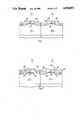
- FIGS. 1 through 4are side view schematic diagrams illustrating the processing steps which are one embodiment of the present invention.
- FIGS. 1 through 4are side view schematic diagrams illustrating the processing steps of one embodiment of the present invention.
- FIG. 1shows N channel transistor 10 and P channel transistor 12, each formed in substrate 14.
- N channel transistor 10is formed in P well 16 and comprises source region 18, gate 20 and drain region 22.
- Gate 20is separated from P well 16 by gate oxide 24.
- Sidewall oxide layers 26are formed on the sides of gate 20.
- P channel transistor 12comprises source region 28, gate 30 and drain region 32.
- Gate 30is separated from N well 34 by gate oxide layer 36.
- Sidewall oxide layers 38are formed on the sides of gate 30.
- Field oxide regions 40separate transistors 10 and 12 from each other and adjacent active devices.
- Titanium layer 42is approximately 1,000 Angstroms thick. Titanium nitride layer 44 is then formed on the surface of titanium layer 42 by sputtering of titanium nitride or chemical vapor deposition of titanium nitride as illustrated in Price, et al., U.S. Pat. No. 4,570,328, issued Feb. 18, 1986.
- the deposition of titanium nitride layer 44is preferably performed in the same reactor used for the deposition of titanium layer 42. Titanium nitride layer 44 is approximately 1,000 Angstroms thick. This minimizes the opportunity for oxygen contact of titanium layer 42 and thus minimizes the formation of titanium oxide.
- FIG. 2The structure of FIG. 2 is then subjected to a heating step in a nitrogen atmosphere at a temperature of approximately 700° C. for approximately 30 minutes. This causes titanium layer 42 to react with the silicon areas of substrate 14 and polycrystalline silicon gates 20 and 30 to form titanium silicide regions 46 as shown in FIG. 3. In addition, the portions of titanium layer 42 which do not react to form titanium silicide combine with titanium nitride layer 44 to provide titanium nitride layer 48.
- Titanium nitride layer 48is then patterned to provide an example interconnection 50 as shown in FIG. 4. The resulting structure is shown in FIG. 4.
Landscapes
- Engineering & Computer Science (AREA)
- Physics & Mathematics (AREA)
- Condensed Matter Physics & Semiconductors (AREA)
- General Physics & Mathematics (AREA)
- Manufacturing & Machinery (AREA)
- Computer Hardware Design (AREA)
- Microelectronics & Electronic Packaging (AREA)
- Power Engineering (AREA)
- Electrodes Of Semiconductors (AREA)
- Internal Circuitry In Semiconductor Integrated Circuit Devices (AREA)
Abstract
Description
The present invention relates to integrated circuits and to methods for manufacturing them.
The present invention relates to the field of integrated circuit technology. More specifically, the present invention relates to a method for providing highly conductive regions in integrated circuitry.
One technique for increasing the conductivity of regions integrated circuitry is direct react silicidation. In direct react silicidation, a layer of metal, such as titanium, is deposited on the surface of an integrated circuit. The structure is then heated to cause the metal to react with the exposed silicon surfaces of the integrated circuit to product titanium silicide. The unreacted metal is then removed by etching. This process is shown in Tasch, et al., U.S. Pat. No. 4,384,301, issued May 17, 1983 and assigned to the assignee of this application. This technique suffers from a shorting problem. During the direct react process, silicon out diffuses into the layer of titanium to provide a titanium silicide bridge between adjacent conductive regions. This causes an unwanted short. One technique for eliminating these unwanted shorts is shown in Lau, U.S. Pat. No. 4,545,116, issued Oct. 8, 1985 and assigned to the assignee of this application. In the method of Lay, the direct reaction step is performed in a nitrogen atmosphere. Titanium reacts with nitrogen to produce titanium nitride, which is relatively easily etched. Thus a competitive reaction process takes place whereby portions of the titanium in contact with the silicon form titanium silicide and those regions that are not in contact with the silicon form titanium nitride. The titanium nitride is then removed by etching.
Another advantage of the titanium nitridation process indirect react silicidation, is that titanium nitride provide a good conductor and thus may be patterned and used as an interconnection in the integrated circuit. This technique is shown in Holloway, et al., U.S. Pat. No. 4,657,628, issued Apr. 14, 1987 and assigned to the assignee of this applicaton. Titanium nitride local interconnect is particularly helpful in the connection of diffused regions of opposite conductivity type. One problem with the use of this local interconnect method is the unequal thicknesses of the local interconnect layer. The titanium layer must be thin enough so that substantial out diffusion and thus shorting between silicided regions does not occur. However, Because this layer is thin, the titanium nitride layer is relatively thin and develops problems with coverage over topography on the integrated circuit.
Another problem with the direct react silicidation process is the formation of titanium oxides. Titanium oxide is a very stable molecule and thus is difficult to etch. Oxide can enter the process by exposure of the titanium coated wafers to the atmosphere or by contaminating oxygen in the reaction chamber. Several methods have been proposed to combat this problem. These methods involve the coding of the titanium layer with various materials. In Tang, et al., U.S. Pat. No. 4,690,730, issued Sept. 31, 1987, a layer of silicon dioxide is formed on the surface of the titanium layer. The layer of silicon dioxide forms a barrier to prevent oxidation of the titanium layer, but some oxide does react with the titanium from the silicon dioxide. Thus, this method is unacceptable.
In Tseng, et al., "a new oxidation-resistance self-aligned TiSi2 process" IEEE Electron Device Letters, Vol. EDL7, No. 11, November 1986, pages 623 and 624, a layer of amorphous silicon is deposited on the surface of the titanium layer. However, this will provide a conductive layer overall which must be patterned to provide the apropriate silicide regions, because the silicon layer will react to provide silicide. Thus, the self-aligned features of direct react silicon as shown in Tasch, et al. are lost.
In Park, et al., "Mo/Ti bilayer metallization for a self-aligned TiSi2 process", Journal of Vacuum Science Technology, April-June 1984, pages 259 through 262, a molybdenum layer is formed on top of the titanium layer. The reference layer suggests that the molybdenum layer provides an effective barrier to prevent the oxidation of the titanium. The experiment in Park, et al. involved the coding of one half of a wafer with the molybdenum titanium stack and leaving the titanium exposed on the other half of the wafer. The results in Park, et al. suggested that the molybdenum provided an effective oxidation barrier. However, further experimentation using a layer of molybdenum overall suggests that the Park, et al. experiment was flawed because of the oxygen consuming effect of the exposed titanium. It has been determined that the molybdenum layer does not provide an effective barrier against oxygen.
The present invention provides a method for inhibiting the oxidation of a titanium layer during the direct reaction of the titanium with exposed silicon areas of an integrated circuit. In one embodiment of the present invention, a titanium nitride layer is formed on the surface of the titanium layer in the reactor where the titanium layer is deposited. The titanium nitride layer provides an effective barrier against oxidation. Thus, the formation of titanium dioxide is inhibited.
In addition, in those areas where titanium nitride local interconnect is to be formed between diffused areas, the extra thickness provided by the top titanium nitride layer adds in the integrity of the conductive layers. By conducting the silicidation in a nitride atmosphere, diffusion of the nitride from the titanium nitride layer into the titanium layer and substitution of those lost nitrogen atoms by the atmosphere occurs thus providing a blocking layer for the formation of titanium silicide shorts.
FIGS. 1 through 4 are side view schematic diagrams illustrating the processing steps which are one embodiment of the present invention.
FIGS. 1 through 4 are side view schematic diagrams illustrating the processing steps of one embodiment of the present invention. FIG. 1 showsN channel transistor 10 andP channel transistor 12, each formed insubstrate 14.N channel transistor 10 is formed inP well 16 and comprisessource region 18,gate 20 anddrain region 22.Gate 20 is separated from P well 16 bygate oxide 24.Sidewall oxide layers 26 are formed on the sides ofgate 20.
A layer of titanium is then sputtered onto the surface of the structure of FIG. 1 to providetitanium layer 42 as shown in FIG. 2.Titanium layer 42 is approximately 1,000 Angstroms thick.Titanium nitride layer 44 is then formed on the surface oftitanium layer 42 by sputtering of titanium nitride or chemical vapor deposition of titanium nitride as illustrated in Price, et al., U.S. Pat. No. 4,570,328, issued Feb. 18, 1986. The deposition oftitanium nitride layer 44 is preferably performed in the same reactor used for the deposition oftitanium layer 42.Titanium nitride layer 44 is approximately 1,000 Angstroms thick. This minimizes the opportunity for oxygen contact oftitanium layer 42 and thus minimizes the formation of titanium oxide.
The structure of FIG. 2 is then subjected to a heating step in a nitrogen atmosphere at a temperature of approximately 700° C. for approximately 30 minutes. This causestitanium layer 42 to react with the silicon areas ofsubstrate 14 andpolycrystalline silicon gates titanium silicide regions 46 as shown in FIG. 3. In addition, the portions oftitanium layer 42 which do not react to form titanium silicide combine withtitanium nitride layer 44 to providetitanium nitride layer 48.
Although specific embodiments of the present invention are disclosed herein, they are not to be construed as limiting the scope of the present invention. The present invention is limited only by the claims appended hereto.
Claims (8)
1. A method for forming high conductivity regions in selected regions of a silicon integrated circuit, comprising the steps of:
depositing a layer of titanium overall said silicon integrated circuit;
depositing a layer of titanium nitride on said layer of titanium;
heating said integrated circuit to a temperature sufficient to cause said layer of titanium to react with said selected regions of said silicon integrated circuit to form titanium silicide;
patterning and etching said layer of titanium nitride to provide conductive titanium nitride connection between elements of said integrated circuit said etching removing said layer of titanium nitride from above said titanium silicide where said silicide is not in contact with said conductive connection;
2. The method of claim 1 wherein said selected regions comprise crystalline silicon.
3. The method of claim 1 wherein said selected regions comprise polycrystalline silicon.
4. A method as in claim 1 wherein said selected regions comprises a layer of polycrystalline silicon separated from the substrate of said integrated circuit by an insulating layer, further comprising the step of forming sidewall oxide layers on the sides of said layer of polycrystalline silicon.
5. A method for forming high conductivity regions in selected regions of a silicon integrated circuit, comprising the steps of:
placing said silicon integrated circuit in a controlled environment chamber and depositing a layer of titanium overall said silicon integrated circuit;
depositing a layer of titanium nitride on said layer of titanium in said chamber without removing said integrated circuit from said chamber;
heating said integrated circuit to a temperature sufficient to cause said layer of titanium to react with said selected regions of said silicon integrated circuit to form titanium silicide;
patterning and etching said layer of titanium nitride to provide conductive titanium nitride connection between elements of said silicon integrated, said etching removing said layer of titanium nitride from above said titanium silicide where said silicide is not in contact with said conductive connection.
6. The method of claim 5 wherein said selected regions comprise crystalline silicon.
7. The method of claim 5 wherein said selected regions comprise polycrystalline silicon.
8. A method as in claim 5 wherein said selected regions comprise a layer of polycrystalline silicon separated from the substrate of said integrated circuit by an insulating layer, further comrising the step of forming sidewall oxide layers on the sides of said layer of polycrystalline silicon.
Priority Applications (2)
| Application Number | Priority Date | Filing Date | Title |
|---|---|---|---|
| US07/350,429US4920073A (en) | 1989-05-11 | 1989-05-11 | Selective silicidation process using a titanium nitride protective layer |
| JP2122773AJP3042857B2 (en) | 1989-05-11 | 1990-05-11 | Method of forming high conductivity region in silicon integrated circuit |
Applications Claiming Priority (1)
| Application Number | Priority Date | Filing Date | Title |
|---|---|---|---|
| US07/350,429US4920073A (en) | 1989-05-11 | 1989-05-11 | Selective silicidation process using a titanium nitride protective layer |
Publications (1)
| Publication Number | Publication Date |
|---|---|
| US4920073Atrue US4920073A (en) | 1990-04-24 |
Family
ID=23376680
Family Applications (1)
| Application Number | Title | Priority Date | Filing Date |
|---|---|---|---|
| US07/350,429Expired - LifetimeUS4920073A (en) | 1989-05-11 | 1989-05-11 | Selective silicidation process using a titanium nitride protective layer |
Country Status (2)
| Country | Link |
|---|---|
| US (1) | US4920073A (en) |
| JP (1) | JP3042857B2 (en) |
Cited By (43)
| Publication number | Priority date | Publication date | Assignee | Title |
|---|---|---|---|---|
| US5086016A (en)* | 1990-10-31 | 1992-02-04 | International Business Machines Corporation | Method of making semiconductor device contact including transition metal-compound dopant source |
| US5166771A (en)* | 1990-01-12 | 1992-11-24 | Paradigm Technology, Inc. | Self-aligning contact and interconnect structure |
| US5196360A (en)* | 1990-10-02 | 1993-03-23 | Micron Technologies, Inc. | Methods for inhibiting outgrowth of silicide in self-aligned silicide process |
| US5229311A (en)* | 1989-03-22 | 1993-07-20 | Intel Corporation | Method of reducing hot-electron degradation in semiconductor devices |
| US5250467A (en)* | 1991-03-29 | 1993-10-05 | Applied Materials, Inc. | Method for forming low resistance and low defect density tungsten contacts to silicon semiconductor wafer |
| US5268590A (en)* | 1989-12-27 | 1993-12-07 | Motorola, Inc. | CMOS device and process |
| US5326724A (en)* | 1991-12-27 | 1994-07-05 | Texas Instruments Incorporated | Oxide-capped titanium silicide formation |
| US5378660A (en)* | 1993-02-12 | 1995-01-03 | Applied Materials, Inc. | Barrier layers and aluminum contacts |
| US5391520A (en)* | 1991-05-03 | 1995-02-21 | Sgs-Thomson Microelectronics, Inc. | Method for forming local interconnect for integrated circuits |
| US5401675A (en)* | 1991-04-19 | 1995-03-28 | Lee; Pei-Ing P. | Method of depositing conductors in high aspect ratio apertures using a collimator |
| US5458697A (en)* | 1990-02-15 | 1995-10-17 | Kabushiki Kaisha Toshiba | Highly purified metal material and sputtering target using the same |
| EP0697723A2 (en) | 1994-08-15 | 1996-02-21 | International Business Machines Corporation | A process for metallization of an insulator layer |
| US5529670A (en)* | 1991-04-19 | 1996-06-25 | International Business Machines Corporation | Method of depositing conductors in high aspect ratio apertures under high temperature conditions |
| US5567651A (en)* | 1992-03-02 | 1996-10-22 | Digital Equipment Corporation | Self-aligned cobalt silicide on MOS integrated circuits |
| US5607884A (en)* | 1993-12-16 | 1997-03-04 | Lg Semicon Co., Ltd. | Method for fabricating MOS transistor having source/drain region of shallow junction and silicide film |
| US5633202A (en)* | 1994-09-30 | 1997-05-27 | Intel Corporation | High tensile nitride layer |
| US5731226A (en)* | 1996-08-17 | 1998-03-24 | United Microelectronics Corporation | Low temperature method of manufacturing epitaxial titanium silicide |
| US5776823A (en)* | 1995-01-12 | 1998-07-07 | Ibm Corporation | Tasin oxygen diffusion barrier in multilayer structures |
| US5834368A (en)* | 1992-02-13 | 1998-11-10 | Nec Corporation | Integrated circuit with a metal silicide film uniformly formed |
| US5858868A (en)* | 1992-05-08 | 1999-01-12 | Yamaha Corporation | Method of manufacturing a laminated wiring structure preventing impurity diffusion therein from N+ and P+ regions in CMOS device with ohmic contact |
| EP0896364A1 (en)* | 1997-08-07 | 1999-02-10 | Lucent Technologies Inc. | Method of making a field-effect transistor with self-aligned TiSi2/TiN source and drain contacts |
| US5877087A (en)* | 1995-11-21 | 1999-03-02 | Applied Materials, Inc. | Low temperature integrated metallization process and apparatus |
| US5877086A (en)* | 1996-07-12 | 1999-03-02 | Applied Materials, Inc. | Metal planarization using a CVD wetting film |
| US5889328A (en)* | 1992-02-26 | 1999-03-30 | International Business Machines Corporation | Refractory metal capped low resistivity metal conductor lines and vias |
| US5902129A (en)* | 1997-04-07 | 1999-05-11 | Lsi Logic Corporation | Process for forming improved cobalt silicide layer on integrated circuit structure using two capping layers |
| US5911114A (en)* | 1997-03-21 | 1999-06-08 | National Semiconductor Corporation | Method of simultaneous formation of salicide and local interconnects in an integrated circuit structure |
| US5989623A (en)* | 1997-08-19 | 1999-11-23 | Applied Materials, Inc. | Dual damascene metallization |
| US6001420A (en)* | 1996-09-23 | 1999-12-14 | Applied Materials, Inc. | Semi-selective chemical vapor deposition |
| US6033978A (en)* | 1994-07-05 | 2000-03-07 | Nec Corporation | Process of selectively producing refractory metal silicide uniform in thickness regardless of conductivity type of silicon thereunder |
| US6066358A (en)* | 1995-11-21 | 2000-05-23 | Applied Materials, Inc. | Blanket-selective chemical vapor deposition using an ultra-thin nucleation layer |
| US6139697A (en)* | 1997-01-31 | 2000-10-31 | Applied Materials, Inc. | Low temperature integrated via and trench fill process and apparatus |
| US6156633A (en)* | 1997-05-17 | 2000-12-05 | United Microelectronics Corp. | Process for forming high temperature stable self-aligned metal silicide layer |
| US6207558B1 (en) | 1999-10-21 | 2001-03-27 | Applied Materials, Inc. | Barrier applications for aluminum planarization |
| US6228777B1 (en) | 1999-06-08 | 2001-05-08 | Intel Corporation | Integrated circuit with borderless contacts |
| GB2319533B (en)* | 1996-11-22 | 2001-06-06 | Trikon Equip Ltd | Methods of forming a barrier layer |
| US6449525B1 (en)* | 1998-09-14 | 2002-09-10 | Applied Materials, Inc. | Computer system to control multiple step ionized metal plasma deposition process for conformal step coverage |
| US6458684B1 (en) | 1995-11-21 | 2002-10-01 | Applied Materials, Inc. | Single step process for blanket-selective CVD aluminum deposition |
| US6537905B1 (en) | 1996-12-30 | 2003-03-25 | Applied Materials, Inc. | Fully planarized dual damascene metallization using copper line interconnect and selective CVD aluminum plug |
| US6605531B1 (en) | 1997-11-26 | 2003-08-12 | Applied Materials, Inc. | Hole-filling technique using CVD aluminum and PVD aluminum integration |
| US20030194850A1 (en)* | 2002-04-16 | 2003-10-16 | Applied Materials, Inc. | Method and apparatus for improved electroplating fill of an aperture |
| US6726776B1 (en) | 1995-11-21 | 2004-04-27 | Applied Materials, Inc. | Low temperature integrated metallization process and apparatus |
| US6743721B2 (en) | 2002-06-10 | 2004-06-01 | United Microelectronics Corp. | Method and system for making cobalt silicide |
| US8803243B2 (en) | 2012-01-03 | 2014-08-12 | International Business Machines Corporation | Complementary metal oxide semiconductor (CMOS) device having gate structures connected by a metal gate conductor |
Citations (8)
| Publication number | Priority date | Publication date | Assignee | Title |
|---|---|---|---|---|
| US4384301A (en)* | 1979-11-07 | 1983-05-17 | Texas Instruments Incorporated | High performance submicron metal-oxide-semiconductor field effect transistor device structure |
| US4545116A (en)* | 1983-05-06 | 1985-10-08 | Texas Instruments Incorporated | Method of forming a titanium disilicide |
| JPS61183942A (en)* | 1985-02-08 | 1986-08-16 | Fujitsu Ltd | Manufacturing method of semiconductor device |
| JPS61212041A (en)* | 1985-03-18 | 1986-09-20 | Hitachi Ltd | Formation of metal silicide electrode and wiring |
| JPS61258447A (en)* | 1985-05-13 | 1986-11-15 | Toshiba Corp | Manufacturing method of semiconductor device |
| US4657628A (en)* | 1985-05-01 | 1987-04-14 | Texas Instruments Incorporated | Process for patterning local interconnects |
| US4687542A (en)* | 1985-10-24 | 1987-08-18 | Texas Instruments Incorporated | Vacuum processing system |
| US4690730A (en)* | 1986-03-07 | 1987-09-01 | Texas Instruments Incorporated | Oxide-capped titanium silicide formation |
- 1989
- 1989-05-11USUS07/350,429patent/US4920073A/ennot_activeExpired - Lifetime
- 1990
- 1990-05-11JPJP2122773Apatent/JP3042857B2/ennot_activeExpired - Fee Related
Patent Citations (8)
| Publication number | Priority date | Publication date | Assignee | Title |
|---|---|---|---|---|
| US4384301A (en)* | 1979-11-07 | 1983-05-17 | Texas Instruments Incorporated | High performance submicron metal-oxide-semiconductor field effect transistor device structure |
| US4545116A (en)* | 1983-05-06 | 1985-10-08 | Texas Instruments Incorporated | Method of forming a titanium disilicide |
| JPS61183942A (en)* | 1985-02-08 | 1986-08-16 | Fujitsu Ltd | Manufacturing method of semiconductor device |
| JPS61212041A (en)* | 1985-03-18 | 1986-09-20 | Hitachi Ltd | Formation of metal silicide electrode and wiring |
| US4657628A (en)* | 1985-05-01 | 1987-04-14 | Texas Instruments Incorporated | Process for patterning local interconnects |
| JPS61258447A (en)* | 1985-05-13 | 1986-11-15 | Toshiba Corp | Manufacturing method of semiconductor device |
| US4687542A (en)* | 1985-10-24 | 1987-08-18 | Texas Instruments Incorporated | Vacuum processing system |
| US4690730A (en)* | 1986-03-07 | 1987-09-01 | Texas Instruments Incorporated | Oxide-capped titanium silicide formation |
Non-Patent Citations (10)
| Title |
|---|
| Lin, et al., "An Environment . . .", J. Electrochem. Soc., vol. 133, No. 11, Nov. 1986, pp. 2386-2389. |
| Lin, et al., An Environment . . . , J. Electrochem. Soc., vol. 133, No. 11, Nov. 1986, pp. 2386 2389.* |
| Park, et al., "Mo/Ti Bilayer . . .", J. Vac. Sci. Technol. A2(2), Apr.-Jun. 1984, pp. 259-263. |
| Park, et al., Mo/Ti Bilayer . . . , J. Vac. Sci. Technol. A2(2), Apr. Jun. 1984, pp. 259 263.* |
| Ting, C. Y., "Silicide for Contacts and Interconnects", IEDM Tech. Digest, 1984, pp. 110-113. |
| Ting, C. Y., Silicide for Contacts and Interconnects , IEDM Tech. Digest, 1984, pp. 110 113.* |
| Tseng, et al., "A New Oxidation . . .", IEEE Electron Device Letters, vol. EDL-7, No. 11, Nov. 1986, pp. 623-624. |
| Tseng, et al., A New Oxidation . . . , IEEE Electron Device Letters, vol. EDL 7, No. 11, Nov. 1986, pp. 623 624.* |
| Wittmer, M., et al., "Applications of TiN . . .", Thin Solid Films, 93 (1982), pp. 397-405. |
| Wittmer, M., et al., Applications of TiN . . . , Thin Solid Films, 93 (1982), pp. 397 405.* |
Cited By (67)
| Publication number | Priority date | Publication date | Assignee | Title |
|---|---|---|---|---|
| US5229311A (en)* | 1989-03-22 | 1993-07-20 | Intel Corporation | Method of reducing hot-electron degradation in semiconductor devices |
| US5268590A (en)* | 1989-12-27 | 1993-12-07 | Motorola, Inc. | CMOS device and process |
| US5166771A (en)* | 1990-01-12 | 1992-11-24 | Paradigm Technology, Inc. | Self-aligning contact and interconnect structure |
| US5458697A (en)* | 1990-02-15 | 1995-10-17 | Kabushiki Kaisha Toshiba | Highly purified metal material and sputtering target using the same |
| US5679983A (en)* | 1990-02-15 | 1997-10-21 | Kabushiki Kaisha Toshiba | Highly purified metal material and sputtering target using the same |
| US5196360A (en)* | 1990-10-02 | 1993-03-23 | Micron Technologies, Inc. | Methods for inhibiting outgrowth of silicide in self-aligned silicide process |
| US5086016A (en)* | 1990-10-31 | 1992-02-04 | International Business Machines Corporation | Method of making semiconductor device contact including transition metal-compound dopant source |
| US5250467A (en)* | 1991-03-29 | 1993-10-05 | Applied Materials, Inc. | Method for forming low resistance and low defect density tungsten contacts to silicon semiconductor wafer |
| US5356835A (en)* | 1991-03-29 | 1994-10-18 | Applied Materials, Inc. | Method for forming low resistance and low defect density tungsten contacts to silicon semiconductor wafer |
| US5529670A (en)* | 1991-04-19 | 1996-06-25 | International Business Machines Corporation | Method of depositing conductors in high aspect ratio apertures under high temperature conditions |
| US5401675A (en)* | 1991-04-19 | 1995-03-28 | Lee; Pei-Ing P. | Method of depositing conductors in high aspect ratio apertures using a collimator |
| US5391520A (en)* | 1991-05-03 | 1995-02-21 | Sgs-Thomson Microelectronics, Inc. | Method for forming local interconnect for integrated circuits |
| US5326724A (en)* | 1991-12-27 | 1994-07-05 | Texas Instruments Incorporated | Oxide-capped titanium silicide formation |
| US5834368A (en)* | 1992-02-13 | 1998-11-10 | Nec Corporation | Integrated circuit with a metal silicide film uniformly formed |
| US6323554B1 (en) | 1992-02-26 | 2001-11-27 | International Business Machines Corporation | Refractory metal capped low resistivity metal conductor lines and vias formed using PVD and CVD |
| US6147402A (en)* | 1992-02-26 | 2000-11-14 | International Business Machines Corporation | Refractory metal capped low resistivity metal conductor lines and vias |
| US5976975A (en)* | 1992-02-26 | 1999-11-02 | International Business Machines Corporation | Refractory metal capped low resistivity metal conductor lines and vias |
| US5889328A (en)* | 1992-02-26 | 1999-03-30 | International Business Machines Corporation | Refractory metal capped low resistivity metal conductor lines and vias |
| US5567651A (en)* | 1992-03-02 | 1996-10-22 | Digital Equipment Corporation | Self-aligned cobalt silicide on MOS integrated circuits |
| US5736461A (en)* | 1992-03-02 | 1998-04-07 | Digital Equipment Corporation | Self-aligned cobalt silicide on MOS integrated circuits |
| US5858868A (en)* | 1992-05-08 | 1999-01-12 | Yamaha Corporation | Method of manufacturing a laminated wiring structure preventing impurity diffusion therein from N+ and P+ regions in CMOS device with ohmic contact |
| US5378660A (en)* | 1993-02-12 | 1995-01-03 | Applied Materials, Inc. | Barrier layers and aluminum contacts |
| US5504043A (en)* | 1993-02-12 | 1996-04-02 | Applied Materials, Inc. | Barrier layers and aluminum contacts |
| US5607884A (en)* | 1993-12-16 | 1997-03-04 | Lg Semicon Co., Ltd. | Method for fabricating MOS transistor having source/drain region of shallow junction and silicide film |
| US6033978A (en)* | 1994-07-05 | 2000-03-07 | Nec Corporation | Process of selectively producing refractory metal silicide uniform in thickness regardless of conductivity type of silicon thereunder |
| EP0697723A2 (en) | 1994-08-15 | 1996-02-21 | International Business Machines Corporation | A process for metallization of an insulator layer |
| US5633202A (en)* | 1994-09-30 | 1997-05-27 | Intel Corporation | High tensile nitride layer |
| US6046494A (en)* | 1994-09-30 | 2000-04-04 | Intel Corporation | High tensile nitride layer |
| US5776823A (en)* | 1995-01-12 | 1998-07-07 | Ibm Corporation | Tasin oxygen diffusion barrier in multilayer structures |
| US6726776B1 (en) | 1995-11-21 | 2004-04-27 | Applied Materials, Inc. | Low temperature integrated metallization process and apparatus |
| US6458684B1 (en) | 1995-11-21 | 2002-10-01 | Applied Materials, Inc. | Single step process for blanket-selective CVD aluminum deposition |
| US6355560B1 (en) | 1995-11-21 | 2002-03-12 | Applied Materials, Inc. | Low temperature integrated metallization process and apparatus |
| US5877087A (en)* | 1995-11-21 | 1999-03-02 | Applied Materials, Inc. | Low temperature integrated metallization process and apparatus |
| US6743714B2 (en) | 1995-11-21 | 2004-06-01 | Applied Materials, Inc. | Low temperature integrated metallization process and apparatus |
| US6066358A (en)* | 1995-11-21 | 2000-05-23 | Applied Materials, Inc. | Blanket-selective chemical vapor deposition using an ultra-thin nucleation layer |
| US5877086A (en)* | 1996-07-12 | 1999-03-02 | Applied Materials, Inc. | Metal planarization using a CVD wetting film |
| US5731226A (en)* | 1996-08-17 | 1998-03-24 | United Microelectronics Corporation | Low temperature method of manufacturing epitaxial titanium silicide |
| US6001420A (en)* | 1996-09-23 | 1999-12-14 | Applied Materials, Inc. | Semi-selective chemical vapor deposition |
| US6430458B1 (en) | 1996-09-23 | 2002-08-06 | Applied Materials, Inc. | Semi-selective chemical vapor deposition |
| GB2319533B (en)* | 1996-11-22 | 2001-06-06 | Trikon Equip Ltd | Methods of forming a barrier layer |
| US7112528B2 (en) | 1996-12-30 | 2006-09-26 | Applied Materials, Inc. | Fully planarized dual damascene metallization using copper line interconnect and selective CVD aluminum plug |
| US20030161943A1 (en)* | 1996-12-30 | 2003-08-28 | Applied Materials, Inc. | Fully planarized dual damascene metallization using copper line interconnect and selective CVD aluminum plug |
| US6537905B1 (en) | 1996-12-30 | 2003-03-25 | Applied Materials, Inc. | Fully planarized dual damascene metallization using copper line interconnect and selective CVD aluminum plug |
| US6139697A (en)* | 1997-01-31 | 2000-10-31 | Applied Materials, Inc. | Low temperature integrated via and trench fill process and apparatus |
| US5911114A (en)* | 1997-03-21 | 1999-06-08 | National Semiconductor Corporation | Method of simultaneous formation of salicide and local interconnects in an integrated circuit structure |
| US5902129A (en)* | 1997-04-07 | 1999-05-11 | Lsi Logic Corporation | Process for forming improved cobalt silicide layer on integrated circuit structure using two capping layers |
| US6156633A (en)* | 1997-05-17 | 2000-12-05 | United Microelectronics Corp. | Process for forming high temperature stable self-aligned metal silicide layer |
| US6670249B1 (en) | 1997-05-17 | 2003-12-30 | United Microelectronics Corp. | Process for forming high temperature stable self-aligned metal silicide layer |
| EP0896364A1 (en)* | 1997-08-07 | 1999-02-10 | Lucent Technologies Inc. | Method of making a field-effect transistor with self-aligned TiSi2/TiN source and drain contacts |
| US5989623A (en)* | 1997-08-19 | 1999-11-23 | Applied Materials, Inc. | Dual damascene metallization |
| US6207222B1 (en) | 1997-08-19 | 2001-03-27 | Applied Materials, Inc. | Dual damascene metallization |
| US6605531B1 (en) | 1997-11-26 | 2003-08-12 | Applied Materials, Inc. | Hole-filling technique using CVD aluminum and PVD aluminum integration |
| US6449525B1 (en)* | 1998-09-14 | 2002-09-10 | Applied Materials, Inc. | Computer system to control multiple step ionized metal plasma deposition process for conformal step coverage |
| US6515351B2 (en) | 1999-06-08 | 2003-02-04 | Intel Corporation | Integrated circuit with borderless contacts |
| US6228777B1 (en) | 1999-06-08 | 2001-05-08 | Intel Corporation | Integrated circuit with borderless contacts |
| US6368880B2 (en)* | 1999-10-21 | 2002-04-09 | Applied Materials, Inc. | Barrier applications for aluminum planarization |
| US6207558B1 (en) | 1999-10-21 | 2001-03-27 | Applied Materials, Inc. | Barrier applications for aluminum planarization |
| US20030194850A1 (en)* | 2002-04-16 | 2003-10-16 | Applied Materials, Inc. | Method and apparatus for improved electroplating fill of an aperture |
| US6797620B2 (en) | 2002-04-16 | 2004-09-28 | Applied Materials, Inc. | Method and apparatus for improved electroplating fill of an aperture |
| US6743721B2 (en) | 2002-06-10 | 2004-06-01 | United Microelectronics Corp. | Method and system for making cobalt silicide |
| US6878627B1 (en) | 2002-06-10 | 2005-04-12 | United Microelectronics Corporation | Semiconductor device with cobalt silicide contacts and method of making the same |
| US20050176248A1 (en)* | 2002-06-10 | 2005-08-11 | Water Lur | Semiconductor device with cobalt silicide contacts |
| US20050179139A1 (en)* | 2002-06-10 | 2005-08-18 | Water Lur | Semiconductor device with cobalt silicide contacts |
| US6943110B1 (en) | 2002-06-10 | 2005-09-13 | United Microelectronics, Corp. | Wafer processing apparatus and methods for depositing cobalt silicide |
| US20060014388A1 (en)* | 2002-06-10 | 2006-01-19 | Water Lur | Wafer processing apparatus & methods for depositing cobalt silicide |
| US8803243B2 (en) | 2012-01-03 | 2014-08-12 | International Business Machines Corporation | Complementary metal oxide semiconductor (CMOS) device having gate structures connected by a metal gate conductor |
| US9082877B2 (en) | 2012-01-03 | 2015-07-14 | International Business Machines Corporation | Complementary metal oxide semiconductor (CMOS) device having gate structures connected by a metal gate conductor |
Also Published As
| Publication number | Publication date |
|---|---|
| JPH0373533A (en) | 1991-03-28 |
| JP3042857B2 (en) | 2000-05-22 |
Similar Documents
| Publication | Publication Date | Title |
|---|---|---|
| US4920073A (en) | Selective silicidation process using a titanium nitride protective layer | |
| KR100302894B1 (en) | Integrated circuit structure with dual thickness cobalt silicide layers and method for its manufacture | |
| US5604140A (en) | Method for forming fine titanium nitride film and method for fabricating semiconductor element using the same | |
| US6562718B1 (en) | Process for forming fully silicided gates | |
| US7078777B2 (en) | Semiconductor device having a low-resistance gate electrode | |
| US5962904A (en) | Gate electrode stack with diffusion barrier | |
| US6136705A (en) | Self-aligned dual thickness cobalt silicide layer formation process | |
| EP0264692B1 (en) | Method of forming a bridge contact | |
| US20020048946A1 (en) | Local interconnect structures for integrated circuits and methods for making the same | |
| US5266156A (en) | Methods of forming a local interconnect and a high resistor polysilicon load by reacting cobalt with polysilicon | |
| KR0162673B1 (en) | Manufacture of conducting layer and semiconductor device | |
| IE53237B1 (en) | Low resistivity composite metallization for semiconductor devices and method therefor | |
| US6602754B1 (en) | Nitrogen implant into nitride spacer to reduce nickel silicide formation on spacer | |
| US6437445B1 (en) | Niobium-near noble metal contact structures for integrated circuits | |
| US20020025676A1 (en) | Salicide formation process | |
| US6100191A (en) | Method for forming self-aligned silicide layers on sub-quarter micron VLSI circuits | |
| KR100280905B1 (en) | Metal Salicide Process Using Ion Metal Plasma Deposition | |
| US6635938B1 (en) | Semiconductor device and manufacturing method thereof | |
| JPH088226B2 (en) | Method for manufacturing semiconductor device | |
| US5698468A (en) | Silicidation process with etch stop | |
| US6686277B1 (en) | Method of manufacturing semiconductor device | |
| JPH10335265A (en) | Manufacture of semiconductor device | |
| JP2908774B2 (en) | Bit line of semiconductor device and method of manufacturing the same | |
| US6403473B1 (en) | Process for producing metal-containing layers | |
| KR0161880B1 (en) | Dense titanium nitride film formation method and semiconductor device manufacturing method using the same |
Legal Events
| Date | Code | Title | Description |
|---|---|---|---|
| AS | Assignment | Owner name:TEXAS INSTRUMENTS INCORPORATED, A CORP. OF DE, TEX Free format text:ASSIGNMENT OF ASSIGNORS INTEREST.;ASSIGNORS:WEI, CHE-CHIA;TANG, THOMAS E.;DOUGLAS, MONTE A.;AND OTHERS;REEL/FRAME:005078/0699;SIGNING DATES FROM 19890503 TO 19890510 | |
| STCF | Information on status: patent grant | Free format text:PATENTED CASE | |
| FEPP | Fee payment procedure | Free format text:PAYOR NUMBER ASSIGNED (ORIGINAL EVENT CODE: ASPN); ENTITY STATUS OF PATENT OWNER: LARGE ENTITY | |
| FPAY | Fee payment | Year of fee payment:4 | |
| FPAY | Fee payment | Year of fee payment:8 | |
| FPAY | Fee payment | Year of fee payment:12 |