US4920070A - Method for forming wirings for a semiconductor device by filling very narrow via holes - Google Patents
Method for forming wirings for a semiconductor device by filling very narrow via holesDownload PDFInfo
- Publication number
- US4920070A US4920070AUS07/127,042US12704287AUS4920070AUS 4920070 AUS4920070 AUS 4920070AUS 12704287 AUS12704287 AUS 12704287AUS 4920070 AUS4920070 AUS 4920070A
- Authority
- US
- United States
- Prior art keywords
- insulating layer
- layer
- metal material
- via holes
- forming
- Prior art date
- Legal status (The legal status is an assumption and is not a legal conclusion. Google has not performed a legal analysis and makes no representation as to the accuracy of the status listed.)
- Expired - Fee Related
Links
Images


Classifications
- H—ELECTRICITY
- H01—ELECTRIC ELEMENTS
- H01L—SEMICONDUCTOR DEVICES NOT COVERED BY CLASS H10
- H01L21/00—Processes or apparatus adapted for the manufacture or treatment of semiconductor or solid state devices or of parts thereof
- H01L21/70—Manufacture or treatment of devices consisting of a plurality of solid state components formed in or on a common substrate or of parts thereof; Manufacture of integrated circuit devices or of parts thereof
- H01L21/71—Manufacture of specific parts of devices defined in group H01L21/70
- H01L21/768—Applying interconnections to be used for carrying current between separate components within a device comprising conductors and dielectrics
- H01L21/76838—Applying interconnections to be used for carrying current between separate components within a device comprising conductors and dielectrics characterised by the formation and the after-treatment of the conductors
- H01L21/76877—Filling of holes, grooves or trenches, e.g. vias, with conductive material
- H01L21/76879—Filling of holes, grooves or trenches, e.g. vias, with conductive material by selective deposition of conductive material in the vias, e.g. selective C.V.D. on semiconductor material, plating
- H—ELECTRICITY
- H01—ELECTRIC ELEMENTS
- H01L—SEMICONDUCTOR DEVICES NOT COVERED BY CLASS H10
- H01L21/00—Processes or apparatus adapted for the manufacture or treatment of semiconductor or solid state devices or of parts thereof
- H01L21/02—Manufacture or treatment of semiconductor devices or of parts thereof
- H01L21/04—Manufacture or treatment of semiconductor devices or of parts thereof the devices having potential barriers, e.g. a PN junction, depletion layer or carrier concentration layer
- H01L21/18—Manufacture or treatment of semiconductor devices or of parts thereof the devices having potential barriers, e.g. a PN junction, depletion layer or carrier concentration layer the devices having semiconductor bodies comprising elements of Group IV of the Periodic Table or AIIIBV compounds with or without impurities, e.g. doping materials
- H01L21/30—Treatment of semiconductor bodies using processes or apparatus not provided for in groups H01L21/20 - H01L21/26
- H01L21/31—Treatment of semiconductor bodies using processes or apparatus not provided for in groups H01L21/20 - H01L21/26 to form insulating layers thereon, e.g. for masking or by using photolithographic techniques; After treatment of these layers; Selection of materials for these layers
- H01L21/3205—Deposition of non-insulating-, e.g. conductive- or resistive-, layers on insulating layers; After-treatment of these layers
- H01L21/321—After treatment
Definitions
- the present inventionrelates to a method for forming wirings and associated via holes of a semiconductor device, and more particularly to a method for forming wirings by irradiating a laser beam on a metal layer sputtered on an insulating layer formed on a semiconductor substrate, with filling via holes previously provided in the insulating layer with melted material of the metal layer, so that the wirings are electrically well connected with the semiconductor substrate through the via holes.
- VLSIvery large scale integration
- wirings of a semiconductor deviceare formed by patterning a metal layer formed by sputtering electrically conductive material, such as aluminum (Al), onto an insulating layer having a plurality of via holes.
- electrically conductive materialsuch as aluminum (Al)
- the via holesare filled with the electrically conductive material while the metal layer is being formed on a surface of the insulating layer.
- Alaluminum
- a laser melting methodhas appeared because the laser melting method is simple in the fabricating process of the semiconductor device, compared with other methods, such as a selective chemical vapor deposition (CVD) method or a bias sputtering method, for planarizing the metal layer.
- the laser melting methodis a method for melting the metal layer by irradiating the layer with a laser beam. And it is expected that when the metal layer is melted by the laser beam, the via holes are sufficiently filled with melted metal while the surface of the metal layer is being planarized. Therefore, the laser melting method will be called the "laser filling method" hereinafter.
- the laser filling methodis new and under development, and there are some reports as to trials of the laser filling method.
- a report as to the laser filling methodwas presented by D. B. Tuckerman and A. H. Weisberg in a paper entitled "Planarization of Gold and Aluminum Thin Films Using a Pulsed Laser", in IEEE Electron Device Lett., vol. EDL-7, pp. 1-4, in 1986.
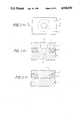
- FIGS. 1(a)-(b)show the general construction of an insulating layer having a via hole, formed on a semiconductor substrate of a semiconductor device such as the VLSI semiconductor device.
- FIG. 1(a)shows a partial plane view of an insulating layer 2 formed on a semiconductor (silicon (Si)) substrate 1 so as to indicate a via hole 3 which is one of a plurality of via holes provided in the insulating layer 2.
- FIG. 1(b)shows a cross sectional view along the line A-A' in FIG. 1(a).
- the insulating layer 2 made of silicon dioxide (SiO 2 ) of 1 ⁇ m thicknessis deposited on a surface, having a (100) surface orientation, of the semiconductor substrate 1. Then, the via hole 3 is formed in the insulating layer 2 by applying a method combining a photolithography method and an etching method.
- the insulating layer 2can also be made of phosphosilicate glass (PSG) or silicon nitride (Si 3 N 4 ).
- PSGphosphosilicate glass
- Si 3 N 4silicon nitride
- FIGS. 2(a)-(c)show construction of a sputtered metal layer 4 formed on an insulating layer, as an example of the prior art, particularly around a via hole 3.
- FIGS. 2(a)-(c)the same reference numerals as in FIGS. 1(a)-(b) designate the same elements as in FIGS. 1(a)-(b).
- FIG. 2(a)shows a partial plan view of the sputtered metal layer 4 around the via hole 3
- FIG. 2(b)shows a cross sectional view along the line B-B' in FIG. 2(a).
- a size of an aperture of the via hole 3is relatively large, such as 3 ⁇ m.
- the sputtered metal layer 4can be formed even on a bottom surface 101, which is a partial surface of the semiconductive substrate 1, of the via hole 3, even though a hollow part 41 is produced on a surface of the metal layer 4 at the via hole 3. Accordingly, when the laser filling method is applied to the surface of the sputtered metal layer 4, the hollow part 41 is planarized and so a planarized metal layer 4' can be formed together with perfectly filling the via hole 3 with a melted metal layer, as shown in FIG. 2(c).
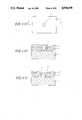
- FIGS. 3(a)-(c)show a case wherein the sputtered metal layer 4 is too thick, and FIGS. 4(a)-(c) show a case of being too thin.
- the same reference numerals as in FIG. 2designate the same elements as in FIG. 2.
- FIGS. 2(a) and 2(b)FIGS.
- FIGS. 3(b) and 4(b)show respectively a partial plan view of the metal layer 4 sputtered on the surface of the insulating layer 2, particularly around a via hole 3, and FIGS. 3(b) and 4(b) show cross sectional views along the line C-C' in FIG. 3(a) and along the line D-D' in FIG. 4(a) respectively.
- each via holehas an aperture size which is too small and an aspect ratio which is too high; and (3) the viscosity of the melted metal is too large when the sputtered metal layer is melted by the laser beam irradiation.
- an object of the present inventionis to improve the planarizing process, performed by using the laser filling method, of the sputtered metal layer, in the fabricating process of the semiconductor device, so as to fill the very narrow via holes associated with the wirings and having an aperture size smaller than 1 ⁇ m and an aspect ratio more than one with the electrically conductive material.
- Another object of the present inventionis to increase the reliability of the semiconductor device having via holes associated with the wirings.
- Still another object of the present inventionis to decrease the fabrication cost of the semiconductor device having via holes associated with the wirings.
- the above objectsare achieved by controlling the quantity of the electrically conductive material for forming the metal layer by the sputtering method so that the calculated thickness of the ideally planarized metal layer is more than 0.5 ⁇ m but not so thick as to generate caves or voids in the via holes after planarizing the sputtered metal layer by applying the laser filling method.
- FIG. 1(a)is a partial plan view of an insulating layer, having a via hole, formed on a semiconductor substrate;
- FIG. 1(b)is a cross-sectional view along the line A-A' in FIG. 1(a);
- FIG. 2(a)is a partial plan view of a sputtered metal layer sputtered on an insulating layer having a large sized via hole and formed on a semiconductor substrate;
- FIG. 2(b)is a cross-sectional view along the line B-B' in FIG. 2(a);
- FIG. 2(c)is a cross-sectional view of a planarized metal layer on the insulating layer formed on the semiconductor substrate in FIG. 2(b), along the line B-B';
- FIG. 3(a)is a partial plan view of a thick sputtered metal layer sputtered by the prior art method on an insulating layer having the small sized via hole and formed on a semiconductor substrate;
- FIG. 3(b)is a cross-sectional view along the line C-C' in FIG. 3(a);
- FIG. 3(c)is a cross-sectional view of a planarized metal layer having a cave in the small sized via hole formed on the insulating layer formed on the semiconductor substrate in FIG. 3(b), along the line C-C';
- FIG. 4(a)is a partial plan view of a thin sputtered metal layer sputtered by the prior art method on an insulating layer, having a small sized via hole, formed on a semiconductor substrate;
- FIG. 4(b)is a cross-sectional view along the line D-D' in FIG. 4(a);
- FIG. 4(c)is a cross-sectional view of a planarized metal layer, having a torn portion of the planarized metal layer around the small sized via hole, formed on the insulating layer on the semiconductor substrate in FIG. 4(b), along the line D-D';
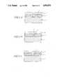
- FIG. 5(a)is a partial plan view of a metal layer sputtered by the method embodying the present invention on an insulating layer having the small sized via hole and formed on a semiconductor substrate;
- FIG. 5(b)is a cross-sectional view along the line E-E' in FIG. 5(a);
- FIG. 5(c)is a cross-sectional view of a planarized metal layer formed on the insulating layer on the semiconductor substrate in FIG. 5(b), along the line E-E';
- FIG. 5(d)is a plan view of the planarized and patterned metal layer in FIG. 5(c);
- FIG. 6(a)is a cross-sectional view of a sputtered metal layer sputtered on an insulating layer having a very small sized via hole and a large aspect ratio;
- FIG. 6(b)is a cross-sectional view of a planarized metal layer formed by planarizing the sputtered metal layer in FIG. 6(a) in circumstances of 200° C., in which a cave appears in the very small sized via hole;
- FIG. 6(c)is a cross-sectional view of the planarized metal layer in circumstances of 300° C., in which no cave appears in the very small sized via hole;
- FIG. 7is a cross-sectional view of a prior art buried wiring connected with via holes
- FIGS. 8(a)-8(h)are for showing fabricating steps, embodying the present invention, of a buried wiring
- FIG. 8(a)is a partial plan view of a double layered insulator having a groove
- FIG. 8(b)is a cross-sectional view along the line F-F' in FIG. 8(a);
- FIG. 8(c)is a plan view of the groove, being the same as the groove in FIG. 8(a), having two via holes in an insulating layer;
- FIG. 8(d)is a cross-sectional view along the line G-G' in FIG. 8(c);
- FIG. 8(e)is a cross-sectional view of a sputtered metal layer sputtered on the via holes and the groove of the insulating layer formed on a semiconductor substrate;
- FIG. 8(f)is a cross-sectional view of a planarized metal layer planarized with filling the via holes with metal;
- FIG. 8(g)is a cross-sectional view of a buried wiring formed by etching the planarized metal layer in FIG. 8(f);
- FIG. 8(h)is a plan view of the buried wiring connected with the via holes
- FIG. 9is a partial cross-sectional view of double layered buried wirings formed by a method embodying the present invention.
- FIG. 10is a graph illustrating results from experiments studying contact resistance against contact sizes of via holes comparing a laser filling method with the prior art methods.
- FIG. 11is a graph illustrating results from experiments studying radiation damage induced by a laser beam in a device.
- the metal layeris melted by the irradiation of the pulsed laser beam
- whether the melted layer is torn from the insulating layer nearby the aperture of the via holemainly depends on: (1) the energy of the pulsed laser beam; (2) the quantity of the instantaneously melted metal layer; (3) the total volume of the via holes provided in the insulating layer in a laser irradiated region; and (4) the viscosity and the surface tension of the melted metal layer.
- the calculated thickness of the metal planarized layerideally must be more than 0.5 ⁇ m for realizing the perfect filling of the via holes in the step for planarizing the sputtered metal layer by irradiation with the pulsed laser beam, and it has been found that when the thickness of the sputtered metal layer is controlled to be properly thin, the problem of the cave occurring in the via hole can be avoided.
- FIGS. 5(a)-5(d)show the fabrication steps of forming the metal layer by the sputtering method (FIGS. 5(a) and 5(b)), planarizing the metal layer together with filling the via holes perfectly by the laser filling method (FIG. 5(c)), and forming wirings (FIG. 5(d)).
- FIGS. 4(a)-4(c)show a partial plan view of a sputtered metal layer 4 onto an insulating layer around a via hole 3
- FIG. 5(b)is a cross-sectional view along the line E-E' in FIG. 5(a)
- FIG. 5(c)is a cross-sectional view for explaining the planarization step along the line E-E'.
- FIG. 5(d)shows the same partial plan view as in FIG. 5(a), but shows a wiring 5 patterned on the insulating layer 2 by pattern etching the planarized metal layer 4' in FIG. 5(c).
- the same reference numerals as in FIGS. 4(a)- 4(c)designate the same elements as in FIGS. 4(a)-4(c).
- An insulating layer 2 made of SiO 2is deposited on a surface, having (100) surface orientation, of an N-type Si substrate 1 so as to have 1 ⁇ m thickness, as shown in FIG. 5(b).
- thirty six cylindrical via holes 3, each having 1 ⁇ m aperture diameter and 1 ⁇ m depth,are provided in the insulating layer 2 so that the 36 via holes 3 are arranged having an equal interval between each other in X and Y directions in a square area of 10 ⁇ m ⁇ 10 ⁇ m.
- FIGS. 5(a)-5(d)one of the 36 via holes is depicted.
- an electrically conductive materialsuch as Al
- a sputtered metal layer 4is formed having 0.8 ⁇ m thickness, as shown in FIGS. 5(a) and 5(b).
- an energy beam 50is irradiated in one pulse on the surface of the sputtered metal layer 4.
- an argon fluoride (ArF) excimer laser beamhaving characteristics of 193 nanometer (nm) wave length, 15 nanosecond (ns) pulse width and 200 milliwatt (mW) peak power is used.
- the sputtered metal layer 4can be planarized so that the planarized metal layer 4' can be formed while perfectly filling the via holes 3 with the melted metal without the formation of caves or the problem of tearing the planarized metal layer 4' in the via hole region.
- a wiring 5is formed on the insulating layer 2 by patterning the planarized metal layer 4' with a method of photolithography as shown in FIG. 5(d).
- the area irradiated by the energy beam 50is 2 mm ⁇ 0.8 mm at the surface of the sputtered metal layer 4, and the above planarizing process is performed under 1 ⁇ 10 -6 Torr vacuum condition for avoiding Al oxidation, or Al oxidation can also be avoided by using a non-oxidizing atmosphere, such as argon, hydrogen, or helium;
- a krypton fluoride (KrF) excimer laser having 248 nm wave length or xenon chloride (XeCl) excimer laser having 308 nm wave lengthcan be used instead of the ArF excimer laser, and when a CW laser, such as an Ar laser or a Kr laser, is to be used, an optical switch element which utilizes a nonlinear optical element for obtaining an optical pulse having a pulse width less than 1 ⁇ s should be used; and
- an Al-Si alloy or an Al-Cu alloycan be used instead of Al under the same condition.
- Different points of the second method from the first methodare as follows: the aperture diameter of each via hole 3 is changed to 0.8 ⁇ m from 1 ⁇ m; the thickness of the sputtered metal layer made of Al is changed to 0.7 ⁇ m from 0.8 ⁇ m; and particularly, the fabricating material having the sputtered metal layer 4 is heated up to 350° C.-400° C. in temperature, for example, by putting it on a heating block.
- Other conditions for the second methodare the same as for the first method.
- the wiringscan be fabricated without producing the problems of caves and torn metal layers. Since the sputtered metal layer is heated up, the melted metal is not cooled so quickly. Accordingly, a time duration during which the viscosity of the melted metal is low is lengthened, even though the sputtered metal layer 4 is irradiated for a very short time, such as 15 ns, by the pulsed laser beam, as stated in the explanation of the first method. Therefore, when the via holes are very narrow, having less than 1 ⁇ m diameter, and have a high aspect ratio, such as more than 2, the second method is effective to fill the via holes with the melted metal perfectly.
- FIGS. 6(a)-6(c)illustrate the effect of heating the sputtered metal layer 4 when the via holes 3 have a 0.8 ⁇ m aperture diameter and a 1.8 ⁇ m depth respectively.
- FIGS. 6(a)-6(c)are cross-sectional views in which a metal layer sputtered on an insulating layer formed on a Si substrate is partially illustrated around a via hole respectively.
- the same reference numerals as in FIGS. 5(a)-5(c)designate the same elements as in FIGS. 5(a)-5(c).
- the sputtered metal layer 4has not yet been irradiated by the pulsed laser beam.
- the planarized metal layer 4'has been formed by the irradiation of the pulsed laser beam during which time the device has been heated to a temperature of 200° C. In this case, a cave 43 has been produced in the via hole 3.
- the planarized metal layer 4'is formed similarly to as in FIG. 6(b), but while the device has been heated to a temperature of 300° C. In this case, the via hole 3 is completely filled with the melted metal.
- the via holes 3can be perfectly filled with the melted metal even though each via hole has a high aspect ratio, such as 2 or 3.
- the temperaturecan not be raised too high, because the electrically conductive material such as Al would have unstable characteristics. For example, it would become easy to be oxidized, and moreover, undesirable tension would be produced between the semiconductor substrate 1 and the insulating layer 2 because of their different coefficients of expansion. Accordingly, due to these possible side effects, as low a temperature as is possible is desirable so that proper filling is accomplished.
- the art of the present inventioncan be extended to apply to a method for forming "buried wirings" in the semiconductor device; wherein the buried wirings are formed in grooves previously formed on a surface of an insulating layer in accordance with a wiring pattern previously designed.
- the wiring formationis performed by filling via holes with the metal of the buried wirings, and the surface of the buried wirings are flattened to conform with the surface of the insulating layer. In this configuration, the via holes are arranged at the bottom of the grooves.
- FIG. 7is a partial cross-sectional view of a buried wiring formed in an insulating layer by the prior art method.
- the same reference numerals as in FIGS. 5(b) and 5(c)designate the same elements.
- the depth of a groove 6is 1 ⁇ m and the depth of each via hole 3 is 1 to 2 ⁇ m. Therefore, the filling of the via holes 3 with the metal, such as Al, corresponds to a case of filling via holes each having a high aspect ratio, such as 2 to 3. In this case, the Al melted by the energy beam irradiation is intended to flow into the via holes 3.
- the melted Altends to solidify before it completely flows into the via holes 3 because of the heat loss due to the heat radiation from the surface of the melted Al, the convection current by the gas surrounding the surface of the melted Al and the heat conduction to the semiconductor substrate 1 through the insulating layer 2. If the melted Al is solidified before it arrives at the bottom of the via hole, the cave 43 appears in the via hole as shown in FIG. 7.
- the above problemcan be solved by improving the insulating layer 2 so as to have a double layered structure combining two insulating layers having different heat conductivity to each other.
- the two insulating layersare composed of a first insulating layer and a second insulating layer.
- the first layeris formed on a semiconductor substrate and the second layer is formed on the first layer so that the groove is made such that the bottom of the groove is formed by the first layer and the upper sides of the groove are formed by the second layer.
- the heat conductivity of the two insulating layersis designed so that the heat conductivity of the second layer is smaller than that of the first layer.
- the temperature of the melted metal (Al) placed at the bottom of the groovefalls first, while the temperature of the melted metal at the upper sides of the groove gradually falls.
- the melted metal at the bottom of the groovechanges to a solid earlier than that at the upper sides of the groove, so that the problem of producing caves in the via holes and sometimes in the groove can be avoided.
- FIGS. 8(a)-(h)show a third method embodying the present invention depicting the fabricating steps of the buried wirings of the semiconductor device; wherein, the buried wirings are formed in the grooves provided in an insulating layer having a double layered structure.
- FIGS. 8(a), 8(c) and 8(h)are partial plan views and FIGS. 8(b) and 8(d)-8(g) are partial cross-sectional views for illustrating the fabricating steps of the buried wirings. Actually, the steps for fabricating only one buried wiring are depicted in FIGS. 8(a)-(h). In FIGS. 8(a)-8(h), the same reference numerals as in FIGS. 5(a)-5(d) designate the same elements as in FIGS. 5(a)-5(d).
- a first insulating layer 21, made of SiO 2is formed on a surface, having (100) surface orientation, of Si substrate 1 so as to have 1 ⁇ m thickness.
- a groove 6is formed in the second layer 22 so that an upper surface of the first layer appears at the bottom face of the groove 6.
- the groove 6is formed so as to have 1-1.5 ⁇ m width, by firstly patterning the wiring pattern on the surface of the second layer 22 by photolithography and then removing the PSG layer in the wiring pattern.
- FIG. 8(a)shows the plan view of FIG. 8(b).
- FIG. 8(c)shows the plan view of FIG. 8(d).
- the electrically conductive material 4is sputtered on the surface shown in FIG. 8(c) by applying, for example, a magnetron sputtering method. Al is used as the electrically conductive material.
- the thickness of the sputtered Al layer 4 shown in FIG. 8(e)should be as thin as possible for carrying out the planarization of the sputtered Al layer without producing the tearing phenomenon on the planarized Al layer.
- the most proper thickness of the sputtered Al layeris determined by considering the volume of the via holes 3 and the grooves 6 to be sputtered and planarized.
- the planarization of the sputtered Al layer 4is carried out by irradiating a pulsed laser beam in a one pulse time duration on the sputtered Al layer 4 in a 1 ⁇ 10 -6 vacuum.
- a pulsed laser beamin a one pulse time duration on the sputtered Al layer 4 in a 1 ⁇ 10 -6 vacuum.
- an ArF excimer laserhaving a 193 nm wave length and having 200 mJ peak energy and 15 ns optical pulse width is used.
- the resulting planarized Al layer 4'is obtained, perfectly filling the groove 6 and the via holes 3 with metal Al as shown in FIG. 8(f). Also, in this case, it has been confirmed that good results can be obtained when the fabricating object is heated up to a maximum of 400° C.
- planarized Al layer 4'is removed and flattened by RIE method, the remaining portion at the groove 6 and the via holes 3 as shown in FIG. 8(g), so that a buried wiring 55 is fabricated as indicated in FIGS. 8(g) and 8(h).
- FIG. 9is a partial cross-sectional view of double layered buried wiring structure in a semiconductor device. These buried wirings 55 can be fabricated by repeating the fabricating steps of the above third method. From this figure, it can be seen that very high integration and very high packing density of the semiconductor device can be realized by applying the third method, and the flattened structure of the buried wirings can be formed with high reliability.
- the first and the second insulating layer 21 and 22other kinds of material can be used if the heat conductivity of the material for the first layer is greater than that for the second layer and the melting points of the material are higher than that of the electrically conductive material 4, for example, the combination of Si 3 N 4 and SiO 2 , borophosphosilicate glass (BPSG) or spin-on-glass (SOG), formed on the first insulating layer 21 constructed of Si 3 N 4 or SiO 2 , can be used as the second insulating layer 22;
- BPSGborophosphosilicate glass
- SOGspin-on-glass
- an Al-Si alloy or an Al-Cu alloycan be used instead of Al;
- a krypton fluoride (KrF) or a xenon chloride (XeCl) excimer lasera helium-cadomium (He-Cd) or an argon (Ar) or a krypton (Kr) gas laser
- KrFkrypton fluoride
- XeClxenon chloride
- He-Cdhelium-cadomium
- Arargon
- Krkrypton
- Krkrypton fluoride
- YAGkrypton
- the first experimentconcerned the contact resistance between Al and Si in a via interconnection.
- a p-type diffused layer having acceptor concentration of more than 10 19 /cm 3is formed on a surface, having (100) surface orientation, of an n-type Si substrate, and the wirings having the via holes are formed on the p-type diffused layer.
- an experiment as to the relation between the Al-Si contact resistance and the via hole diameteris conducted comparing a case of forming wirings by the prior art method, such as a method with usual furnace alloying, and that by the above method of using the laser filling.
- the results of the experimentare shown in FIG. 10.
- FIG. 10a case of performing only the Al sputtering is also indicated for comparing with other cases of the prior art method and the laser filling method.
- the contact resistance for both the prior art method and the laser filling methodis smaller than that when only the Al sputtering is performed, which may be a matter of cause. Further, the contact resistance when the laser filling method is used is smaller than when the prior art method is applied, and the difference between contact resistance becomes greater as the contact size is decreased, particularly for the size less than 2 ⁇ m. As seen from FIG. 10, in the case of the prior art method, there is no datum for the contact resistance for a size of less than 1 ⁇ m. The datum as to 0.7 ⁇ m contact size was obtained for the first time when the method of the present invention was established for filling the via holes completely with the metal.
- the second experiment illustratedconcerns the damage to the semiconductor substrate caused by the laser beam irradiation.
- diodesare fabricated at the p-n junctions so that their sizes are matched to the aperture sizes of via holes respectively.
- the via holesare formed on the diodes so as to have several aperture sizes respectively, and wirings are formed while filling the via holes with the metal (Al) of the wirings.
- the wiring formationis performed by only sputtering Al as a first case, applying a usual furnace alloying method (prior art method) after the Al sputtering as a second case, and applying the laser filling method after the Al sputtering as a third case.
- the ArF excimer laserhaving characteristics of 193 nm wave length and 5 J/cm 2 energy, is used with one shot pulse having 15 ns time duration. Then, leak currents flowing through the diodes are measured. An increase of the leak current indicates an increased amount of damage. The results of the measurements are shown in FIG. 11.
- the present inventionoffers an excellent method for fabricating minute wirings of a semiconductor device, particularly of an LSI or VLSI device.
Landscapes
- Engineering & Computer Science (AREA)
- Physics & Mathematics (AREA)
- Condensed Matter Physics & Semiconductors (AREA)
- General Physics & Mathematics (AREA)
- Manufacturing & Machinery (AREA)
- Computer Hardware Design (AREA)
- Microelectronics & Electronic Packaging (AREA)
- Power Engineering (AREA)
- Internal Circuitry In Semiconductor Integrated Circuit Devices (AREA)
Abstract
Description
Claims (26)
Applications Claiming Priority (4)
| Application Number | Priority Date | Filing Date | Title |
|---|---|---|---|
| JP3630387AJPS63204630A (en) | 1987-02-19 | 1987-02-19 | Manufacturing method of wiring structure |
| JP62-036303 | 1987-02-19 | ||
| JP62-046031 | 1987-02-27 | ||
| JP4603187AJP2598638B2 (en) | 1987-02-27 | 1987-02-27 | Manufacturing method of wiring structure |
Publications (1)
| Publication Number | Publication Date |
|---|---|
| US4920070Atrue US4920070A (en) | 1990-04-24 |
Family
ID=26375338
Family Applications (1)
| Application Number | Title | Priority Date | Filing Date |
|---|---|---|---|
| US07/127,042Expired - Fee RelatedUS4920070A (en) | 1987-02-19 | 1987-11-27 | Method for forming wirings for a semiconductor device by filling very narrow via holes |
Country Status (1)
| Country | Link |
|---|---|
| US (1) | US4920070A (en) |
Cited By (38)
| Publication number | Priority date | Publication date | Assignee | Title |
|---|---|---|---|---|
| US5011793A (en)* | 1990-06-19 | 1991-04-30 | Nihon Shinku Gijutsu Kabushiki Kaisha | Vacuum deposition using pressurized reflow process |
| EP0463731A1 (en)* | 1990-05-31 | 1992-01-02 | Canon Kabushiki Kaisha | Electrode for semiconductor device and process for producing the same |
| FR2664295A1 (en)* | 1990-07-03 | 1992-01-10 | Samsung Electronics Co Ltd | METHOD OF FORMING A METAL LAYER THROUGH A CONTACT HOLE. |
| US5093279A (en)* | 1991-02-01 | 1992-03-03 | International Business Machines Corporation | Laser ablation damascene process |
| GB2247781A (en)* | 1990-09-05 | 1992-03-11 | Micron Technology Inc | Anti-reflective coating for laser planarization of metal layers |
| US5100834A (en)* | 1990-03-20 | 1992-03-31 | Fujitsu Limited | Method of planarizing metal layer |
| US5110759A (en)* | 1988-12-20 | 1992-05-05 | Fujitsu Limited | Conductive plug forming method using laser planarization |
| GB2253939A (en)* | 1991-03-20 | 1992-09-23 | Samsung Electronics Co Ltd | Forming a metal layer on a semiconductor device |
| US5155064A (en)* | 1989-03-20 | 1992-10-13 | Fujitsu Limited | Fabrication method of a semiconductor device having a planarized surface |
| US5169800A (en)* | 1989-12-26 | 1992-12-08 | Fujitsu Limited | Method of fabricating semiconductor devices by laser planarization of metal layer |
| US5219790A (en)* | 1991-07-17 | 1993-06-15 | Sharp Kabushiki Kaisha | Method for forming metallization layer of wiring in semiconductor integrated circuits |
| US5225358A (en)* | 1991-06-06 | 1993-07-06 | Lsi Logic Corporation | Method of forming late isolation with polishing |
| US5232674A (en)* | 1989-12-20 | 1993-08-03 | Fujitsu Limited | Method of improving surface morphology of laser irradiated surface |
| US5248625A (en)* | 1991-06-06 | 1993-09-28 | Lsi Logic Corporation | Techniques for forming isolation structures |
| US5252503A (en)* | 1991-06-06 | 1993-10-12 | Lsi Logic Corporation | Techniques for forming isolation structures |
| US5260232A (en)* | 1991-04-05 | 1993-11-09 | Sony Corporation | Refractory metal plug forming method |
| US5288664A (en)* | 1990-07-11 | 1994-02-22 | Fujitsu Ltd. | Method of forming wiring of semiconductor device |
| US5298110A (en)* | 1991-06-06 | 1994-03-29 | Lsi Logic Corporation | Trench planarization techniques |
| US5409862A (en)* | 1992-03-24 | 1995-04-25 | Kabushiki Kaisha Toshiba | Method for making aluminum single crystal interconnections on insulators |
| US5413966A (en)* | 1990-12-20 | 1995-05-09 | Lsi Logic Corporation | Shallow trench etch |
| US5527561A (en)* | 1991-05-28 | 1996-06-18 | Electrotech Limited | Method for filing substrate recesses using elevated temperature and pressure |
| US5529953A (en)* | 1994-10-14 | 1996-06-25 | Toshiba America Electronic Components, Inc. | Method of forming studs and interconnects in a multi-layered semiconductor device |
| US5633195A (en)* | 1994-08-31 | 1997-05-27 | International Business Machines, Corp. | Laser planarization of zone 1 deposited metal films for submicron metal interconnects |
| DE19600400A1 (en)* | 1996-01-08 | 1997-07-17 | Siemens Ag | Micromechanical component with planarized cover on a cavity and manufacturing process |
| US5828134A (en)* | 1994-05-11 | 1998-10-27 | United Microelectronics Corporation | Metallization to improve electromigration resistance |
| US5891803A (en)* | 1996-06-26 | 1999-04-06 | Intel Corporation | Rapid reflow of conductive layers by directional sputtering for interconnections in integrated circuits |
| US6060385A (en)* | 1997-02-14 | 2000-05-09 | Micro Technology, Inc. | Method of making an interconnect structure |
| US6064084A (en)* | 1996-10-15 | 2000-05-16 | Fujitsu Limited | Semiconductor device having a reliable contact structure |
| US6090636A (en)* | 1998-02-26 | 2000-07-18 | Micron Technology, Inc. | Integrated circuits using optical waveguide interconnects formed through a semiconductor wafer and methods for forming same |
| US6137179A (en)* | 1998-07-24 | 2000-10-24 | Taiwan Semiconductor Manufacturing Company | Method for fabricating capacitor-over-bit line (COB) dynamic random access memory (DRAM) using tungsten landing plug contacts and TI/TIN bit lines |
| US6150188A (en)* | 1998-02-26 | 2000-11-21 | Micron Technology Inc. | Integrated circuits using optical fiber interconnects formed through a semiconductor wafer and methods for forming same |
| US6198168B1 (en)* | 1998-01-20 | 2001-03-06 | Micron Technologies, Inc. | Integrated circuits using high aspect ratio vias through a semiconductor wafer and method for forming same |
| US20010050413A1 (en)* | 1999-04-15 | 2001-12-13 | Li Li | Method of controlling striations and CD loss in contact oxide etch |
| US6355554B1 (en) | 1995-07-20 | 2002-03-12 | Samsung Electronics Co., Ltd. | Methods of forming filled interconnections in microelectronic devices |
| US6395627B1 (en)* | 1999-10-20 | 2002-05-28 | Sony Corporation | Semiconductor device a burried wiring structure and process for fabricating the same |
| US6664626B2 (en)* | 2000-08-01 | 2003-12-16 | Fuji Photo Film Co., Ltd. | Semiconductor device and method of manufacturing the same |
| US20050020095A1 (en)* | 2001-08-23 | 2005-01-27 | Johannes Baur | Method for surface treating a semiconductor |
| US20050048770A1 (en)* | 2003-08-25 | 2005-03-03 | Shinko Electric Industries Co., Ltd. | Process for manufacturing a wiring board having a via |
Citations (11)
| Publication number | Priority date | Publication date | Assignee | Title |
|---|---|---|---|---|
| JPS55162244A (en)* | 1979-06-01 | 1980-12-17 | Mitsubishi Electric Corp | Forming method of metal wiring |
| US4261764A (en)* | 1979-10-01 | 1981-04-14 | The United States Of America As Represented By The United States Department Of Energy | Laser method for forming low-resistance ohmic contacts on semiconducting oxides |
| US4327476A (en)* | 1979-12-07 | 1982-05-04 | Tokyo Shibaura Denki Kabushiki Kaisha | Method of manufacturing semiconductor devices |
| JPS5996746A (en)* | 1982-11-26 | 1984-06-04 | Hitachi Ltd | Semiconductor device and its manufacturing method |
| US4562640A (en)* | 1983-04-25 | 1986-01-07 | Siemens Aktiengesellschaft | Method of manufacturing stable, low resistance contacts in integrated semiconductor circuits |
| JPS6188543A (en)* | 1984-10-08 | 1986-05-06 | Nec Corp | Manufacture of semiconductor device |
| JPS6193650A (en)* | 1984-10-15 | 1986-05-12 | Nec Corp | Manufacture of semiconductor device |
| US4592802A (en)* | 1984-04-13 | 1986-06-03 | Societe Pour L'etude et la Fabrication des Circuits Integres Speciaux E.F.C.I.S. | Method of fabrication of aluminum contacts through a thick insulating layer in an integrated circuit |
| JPS61152040A (en)* | 1984-12-26 | 1986-07-10 | Hitachi Micro Comput Eng Ltd | Manufacture of semiconductor device |
| US4758533A (en)* | 1987-09-22 | 1988-07-19 | Xmr Inc. | Laser planarization of nonrefractory metal during integrated circuit fabrication |
| US4800179A (en)* | 1986-06-13 | 1989-01-24 | Fujitsu Limited | Method for fabricating semiconductor device |
- 1987
- 1987-11-27USUS07/127,042patent/US4920070A/ennot_activeExpired - Fee Related
Patent Citations (11)
| Publication number | Priority date | Publication date | Assignee | Title |
|---|---|---|---|---|
| JPS55162244A (en)* | 1979-06-01 | 1980-12-17 | Mitsubishi Electric Corp | Forming method of metal wiring |
| US4261764A (en)* | 1979-10-01 | 1981-04-14 | The United States Of America As Represented By The United States Department Of Energy | Laser method for forming low-resistance ohmic contacts on semiconducting oxides |
| US4327476A (en)* | 1979-12-07 | 1982-05-04 | Tokyo Shibaura Denki Kabushiki Kaisha | Method of manufacturing semiconductor devices |
| JPS5996746A (en)* | 1982-11-26 | 1984-06-04 | Hitachi Ltd | Semiconductor device and its manufacturing method |
| US4562640A (en)* | 1983-04-25 | 1986-01-07 | Siemens Aktiengesellschaft | Method of manufacturing stable, low resistance contacts in integrated semiconductor circuits |
| US4592802A (en)* | 1984-04-13 | 1986-06-03 | Societe Pour L'etude et la Fabrication des Circuits Integres Speciaux E.F.C.I.S. | Method of fabrication of aluminum contacts through a thick insulating layer in an integrated circuit |
| JPS6188543A (en)* | 1984-10-08 | 1986-05-06 | Nec Corp | Manufacture of semiconductor device |
| JPS6193650A (en)* | 1984-10-15 | 1986-05-12 | Nec Corp | Manufacture of semiconductor device |
| JPS61152040A (en)* | 1984-12-26 | 1986-07-10 | Hitachi Micro Comput Eng Ltd | Manufacture of semiconductor device |
| US4800179A (en)* | 1986-06-13 | 1989-01-24 | Fujitsu Limited | Method for fabricating semiconductor device |
| US4758533A (en)* | 1987-09-22 | 1988-07-19 | Xmr Inc. | Laser planarization of nonrefractory metal during integrated circuit fabrication |
Non-Patent Citations (3)
| Title |
|---|
| Tuckerman et al. , " Planarization of Gold & Aluminium Thin Films Using a Pulsed Laser", IEEE Electron Device Letters, Vol. EDL-7, No. 1, January 1986.* |
| Tuckerman et al., Solid State Technology, (Apr. 1986), pp. 129 134.* |
| Tuckerman et al., Solid State Technology, (Apr. 1986), pp. 129-134. |
Cited By (67)
| Publication number | Priority date | Publication date | Assignee | Title |
|---|---|---|---|---|
| US5110759A (en)* | 1988-12-20 | 1992-05-05 | Fujitsu Limited | Conductive plug forming method using laser planarization |
| US5155064A (en)* | 1989-03-20 | 1992-10-13 | Fujitsu Limited | Fabrication method of a semiconductor device having a planarized surface |
| US5232674A (en)* | 1989-12-20 | 1993-08-03 | Fujitsu Limited | Method of improving surface morphology of laser irradiated surface |
| US5169800A (en)* | 1989-12-26 | 1992-12-08 | Fujitsu Limited | Method of fabricating semiconductor devices by laser planarization of metal layer |
| US5100834A (en)* | 1990-03-20 | 1992-03-31 | Fujitsu Limited | Method of planarizing metal layer |
| EP0463731A1 (en)* | 1990-05-31 | 1992-01-02 | Canon Kabushiki Kaisha | Electrode for semiconductor device and process for producing the same |
| US6218223B1 (en)* | 1990-05-31 | 2001-04-17 | Canon Kabushiki Kaisha | Process for producing electrode for semiconductor element and semiconductor device having the electrode |
| US5233224A (en)* | 1990-05-31 | 1993-08-03 | Canon Kabushiki Kaisha | Electrode having an improved configuration for a semiconductor element |
| US5011793A (en)* | 1990-06-19 | 1991-04-30 | Nihon Shinku Gijutsu Kabushiki Kaisha | Vacuum deposition using pressurized reflow process |
| FR2664295A1 (en)* | 1990-07-03 | 1992-01-10 | Samsung Electronics Co Ltd | METHOD OF FORMING A METAL LAYER THROUGH A CONTACT HOLE. |
| US5288664A (en)* | 1990-07-11 | 1994-02-22 | Fujitsu Ltd. | Method of forming wiring of semiconductor device |
| GB2247781A (en)* | 1990-09-05 | 1992-03-11 | Micron Technology Inc | Anti-reflective coating for laser planarization of metal layers |
| GB2247781B (en)* | 1990-09-05 | 1995-01-11 | Micron Technology Inc | Method for improving step coverage of a metallization layer on an integrated circuit |
| US5413966A (en)* | 1990-12-20 | 1995-05-09 | Lsi Logic Corporation | Shallow trench etch |
| EP0497180A3 (en)* | 1991-02-01 | 1993-04-28 | International Business Machines Corporation | Laser ablation damascene process |
| US5093279A (en)* | 1991-02-01 | 1992-03-03 | International Business Machines Corporation | Laser ablation damascene process |
| GB2253939A (en)* | 1991-03-20 | 1992-09-23 | Samsung Electronics Co Ltd | Forming a metal layer on a semiconductor device |
| US5266521A (en)* | 1991-03-20 | 1993-11-30 | Samsung Electronics Co., Ltd. | Method for forming a planarized composite metal layer in a semiconductor device |
| GB2253939B (en)* | 1991-03-20 | 1995-04-12 | Samsung Electronics Co Ltd | Method for manufacturing a semiconductor device |
| US5260232A (en)* | 1991-04-05 | 1993-11-09 | Sony Corporation | Refractory metal plug forming method |
| US5527561A (en)* | 1991-05-28 | 1996-06-18 | Electrotech Limited | Method for filing substrate recesses using elevated temperature and pressure |
| US5252503A (en)* | 1991-06-06 | 1993-10-12 | Lsi Logic Corporation | Techniques for forming isolation structures |
| US5312770A (en)* | 1991-06-06 | 1994-05-17 | Lsi Logic Corporation | Techniques for forming isolation structures |
| US5298110A (en)* | 1991-06-06 | 1994-03-29 | Lsi Logic Corporation | Trench planarization techniques |
| US5248625A (en)* | 1991-06-06 | 1993-09-28 | Lsi Logic Corporation | Techniques for forming isolation structures |
| US5441094A (en)* | 1991-06-06 | 1995-08-15 | Lsi Logic Corporation | Trench planarization techniques |
| US5471091A (en)* | 1991-06-06 | 1995-11-28 | Lsi Logic Corporation | Techniques for via formation and filling |
| US5225358A (en)* | 1991-06-06 | 1993-07-06 | Lsi Logic Corporation | Method of forming late isolation with polishing |
| US5219790A (en)* | 1991-07-17 | 1993-06-15 | Sharp Kabushiki Kaisha | Method for forming metallization layer of wiring in semiconductor integrated circuits |
| US5409862A (en)* | 1992-03-24 | 1995-04-25 | Kabushiki Kaisha Toshiba | Method for making aluminum single crystal interconnections on insulators |
| US5828134A (en)* | 1994-05-11 | 1998-10-27 | United Microelectronics Corporation | Metallization to improve electromigration resistance |
| US5633195A (en)* | 1994-08-31 | 1997-05-27 | International Business Machines, Corp. | Laser planarization of zone 1 deposited metal films for submicron metal interconnects |
| US5689140A (en)* | 1994-10-14 | 1997-11-18 | Kabushiki Kaisha Toshiba | Method for forming studs and interconnects in a multi-layered semiconductor device |
| US5529953A (en)* | 1994-10-14 | 1996-06-25 | Toshiba America Electronic Components, Inc. | Method of forming studs and interconnects in a multi-layered semiconductor device |
| US6355554B1 (en) | 1995-07-20 | 2002-03-12 | Samsung Electronics Co., Ltd. | Methods of forming filled interconnections in microelectronic devices |
| DE19600400A1 (en)* | 1996-01-08 | 1997-07-17 | Siemens Ag | Micromechanical component with planarized cover on a cavity and manufacturing process |
| DE19600400C2 (en)* | 1996-01-08 | 2002-05-16 | Infineon Technologies Ag | Micromechanical component with planarized cover on a cavity and manufacturing process |
| US5891803A (en)* | 1996-06-26 | 1999-04-06 | Intel Corporation | Rapid reflow of conductive layers by directional sputtering for interconnections in integrated circuits |
| US6064084A (en)* | 1996-10-15 | 2000-05-16 | Fujitsu Limited | Semiconductor device having a reliable contact structure |
| US6060385A (en)* | 1997-02-14 | 2000-05-09 | Micro Technology, Inc. | Method of making an interconnect structure |
| US20050230832A1 (en)* | 1997-02-14 | 2005-10-20 | Micron Technology, Inc. | Three-level unitary interconnect structure |
| US6709978B2 (en) | 1998-01-20 | 2004-03-23 | Micron Technology, Inc. | Method for forming integrated circuits using high aspect ratio vias through a semiconductor wafer |
| US6198168B1 (en)* | 1998-01-20 | 2001-03-06 | Micron Technologies, Inc. | Integrated circuits using high aspect ratio vias through a semiconductor wafer and method for forming same |
| US20070114543A1 (en)* | 1998-02-26 | 2007-05-24 | Micron Technology, Inc. | Electronic systems using optical waveguide interconnects formed through a semiconductor wafer |
| US6150188A (en)* | 1998-02-26 | 2000-11-21 | Micron Technology Inc. | Integrated circuits using optical fiber interconnects formed through a semiconductor wafer and methods for forming same |
| US7547954B2 (en) | 1998-02-26 | 2009-06-16 | Micron Technology, Inc. | Electronic systems using optical waveguide interconnects formed through a semiconductor wafer |
| US6526191B1 (en) | 1998-02-26 | 2003-02-25 | Micron Technology, Inc. | Integrated circuits using optical fiber interconnects formed through a semiconductor wafer and methods for forming same |
| US20030197186A1 (en)* | 1998-02-26 | 2003-10-23 | Micron Technology, Inc. | Integrated circuits using optical waveguide interconnects formed through a semiconductor wafer and methods for forming same |
| US6995441B2 (en) | 1998-02-26 | 2006-02-07 | Micron Technology, Inc. | Integrated circuits using optical waveguide interconnects formed through a semiconductor wafer and methods for forming same |
| US6723577B1 (en) | 1998-02-26 | 2004-04-20 | Micron Technology, Inc. | Method of forming an optical fiber interconnect through a semiconductor wafer |
| US6777715B1 (en) | 1998-02-26 | 2004-08-17 | Micron Technology, Inc. | Integrated circuits using optical waveguide interconnects formed through a semiconductor wafer and methods for forming same |
| US7164156B2 (en) | 1998-02-26 | 2007-01-16 | Micron Technology, Inc. | Electronic systems using optical waveguide interconnects formed throught a semiconductor wafer |
| US20060131684A1 (en)* | 1998-02-26 | 2006-06-22 | Micron Technology, Inc. | Integrated circuits using optical waveguide interconnects formed through a semiconductor wafer and methods for forming same |
| US6995443B2 (en) | 1998-02-26 | 2006-02-07 | Micron Technology, Inc. | Integrated circuits using optical fiber interconnects formed through a semiconductor wafer |
| US6090636A (en)* | 1998-02-26 | 2000-07-18 | Micron Technology, Inc. | Integrated circuits using optical waveguide interconnects formed through a semiconductor wafer and methods for forming same |
| US6137179A (en)* | 1998-07-24 | 2000-10-24 | Taiwan Semiconductor Manufacturing Company | Method for fabricating capacitor-over-bit line (COB) dynamic random access memory (DRAM) using tungsten landing plug contacts and TI/TIN bit lines |
| US20060252198A1 (en)* | 1999-04-15 | 2006-11-09 | Li Li | Method of plasma etching a substrate |
| US20050056875A1 (en)* | 1999-04-15 | 2005-03-17 | Li Li | Method of plasma etching a substrate |
| US7122480B2 (en) | 1999-04-15 | 2006-10-17 | Micron Technology, Inc. | Method of plasma etching a substrate |
| US20010050413A1 (en)* | 1999-04-15 | 2001-12-13 | Li Li | Method of controlling striations and CD loss in contact oxide etch |
| US7470625B2 (en) | 1999-04-15 | 2008-12-30 | Micron Technology, Inc. | Method of plasma etching a substrate |
| US8093155B2 (en) | 1999-04-15 | 2012-01-10 | Micron Technology, Inc. | Method of controlling striations and CD loss in contact oxide etch |
| US6395627B1 (en)* | 1999-10-20 | 2002-05-28 | Sony Corporation | Semiconductor device a burried wiring structure and process for fabricating the same |
| US6664626B2 (en)* | 2000-08-01 | 2003-12-16 | Fuji Photo Film Co., Ltd. | Semiconductor device and method of manufacturing the same |
| US20050020095A1 (en)* | 2001-08-23 | 2005-01-27 | Johannes Baur | Method for surface treating a semiconductor |
| US20050048770A1 (en)* | 2003-08-25 | 2005-03-03 | Shinko Electric Industries Co., Ltd. | Process for manufacturing a wiring board having a via |
| US7205230B2 (en)* | 2003-08-25 | 2007-04-17 | Shinko Electric Industries Co., Ltd. | Process for manufacturing a wiring board having a via |
Similar Documents
| Publication | Publication Date | Title |
|---|---|---|
| US4920070A (en) | Method for forming wirings for a semiconductor device by filling very narrow via holes | |
| US4800179A (en) | Method for fabricating semiconductor device | |
| KR0123887B1 (en) | Manufacturing Method of Semiconductor Device | |
| DE60034611T2 (en) | Vertical fuse and its manufacturing process | |
| US5087589A (en) | Selectively programmable interconnections in multilayer integrated circuits | |
| US5124780A (en) | Conductive contact plug and a method of forming a conductive contact plug in an integrated circuit using laser planarization | |
| US5380678A (en) | Bilayer barrier metal method for obtaining 100% step-coverage in contact vias without junction degradation | |
| US6835657B2 (en) | Method for recrystallizing metal in features of a semiconductor chip | |
| US7217650B1 (en) | Metallic nanowire interconnections for integrated circuit fabrication | |
| US4960729A (en) | Integrated circuits and a method for manufacture thereof | |
| US5250465A (en) | Method of manufacturing semiconductor devices | |
| US4968643A (en) | Method for fabricating an activatable conducting link for metallic conductive wiring in a semiconductor device | |
| EP0208463A1 (en) | Planarization of metal films for multilevel interconnects | |
| JP3050161B2 (en) | Semiconductor device and manufacturing method thereof | |
| JPH07211776A (en) | Formation of conductor path on semiconductor substrate | |
| JPH09139429A (en) | Method for manufacturing semiconductor device | |
| US4976809A (en) | Method of forming an aluminum conductor with highly oriented grain structure | |
| US5288664A (en) | Method of forming wiring of semiconductor device | |
| US4673592A (en) | Metal planarization process | |
| Mukai et al. | High-aspect-ratio via-hole filling with aluminum melting by excimer laser irradiation for multilevel interconnection | |
| JP3583562B2 (en) | Semiconductor device | |
| KR100517350B1 (en) | Method for fabricating hybrid metal interconnect | |
| JP2598638B2 (en) | Manufacturing method of wiring structure | |
| Liu et al. | A study of pulsed laser planarization of aluminum for VLSI metallization | |
| Mukai et al. | Via hole filling with metal melting by laser irradiation for submicron metallization |
Legal Events
| Date | Code | Title | Description |
|---|---|---|---|
| AS | Assignment | Owner name:FUJITSU LIMITED, 1015, KAMIKODANAKA, NAKAHARA-KU, Free format text:ASSIGNMENT OF ASSIGNORS INTEREST.;ASSIGNOR:MUKAI, RYOICHI;REEL/FRAME:004797/0809 Effective date:19871119 Owner name:FUJITSU LIMITED, 1015, KAMIKODANAKA, NAKAHARA-KU, Free format text:ASSIGNMENT OF ASSIGNORS INTEREST;ASSIGNOR:MUKAI, RYOICHI;REEL/FRAME:004797/0809 Effective date:19871119 | |
| CC | Certificate of correction | ||
| FEPP | Fee payment procedure | Free format text:PAYOR NUMBER ASSIGNED (ORIGINAL EVENT CODE: ASPN); ENTITY STATUS OF PATENT OWNER: LARGE ENTITY | |
| FEPP | Fee payment procedure | Free format text:PAYOR NUMBER ASSIGNED (ORIGINAL EVENT CODE: ASPN); ENTITY STATUS OF PATENT OWNER: LARGE ENTITY Free format text:PAYER NUMBER DE-ASSIGNED (ORIGINAL EVENT CODE: RMPN); ENTITY STATUS OF PATENT OWNER: LARGE ENTITY | |
| FPAY | Fee payment | Year of fee payment:4 | |
| FPAY | Fee payment | Year of fee payment:8 | |
| LAPS | Lapse for failure to pay maintenance fees | ||
| LAPS | Lapse for failure to pay maintenance fees | Free format text:PATENT EXPIRED FOR FAILURE TO PAY MAINTENANCE FEES (ORIGINAL EVENT CODE: EXP.); ENTITY STATUS OF PATENT OWNER: LARGE ENTITY | |
| STCH | Information on status: patent discontinuation | Free format text:PATENT EXPIRED DUE TO NONPAYMENT OF MAINTENANCE FEES UNDER 37 CFR 1.362 | |
| FP | Lapsed due to failure to pay maintenance fee | Effective date:20020424 |