US4919521A - Electromagnetic device - Google Patents
Electromagnetic deviceDownload PDFInfo
- Publication number
- US4919521A US4919521AUS07/203,797US20379788AUS4919521AUS 4919521 AUS4919521 AUS 4919521AUS 20379788 AUS20379788 AUS 20379788AUS 4919521 AUS4919521 AUS 4919521A
- Authority
- US
- United States
- Prior art keywords
- particles
- anisotropic particles
- micro
- suspension
- anisotropic
- Prior art date
- Legal status (The legal status is an assumption and is not a legal conclusion. Google has not performed a legal analysis and makes no representation as to the accuracy of the status listed.)
- Expired - Lifetime
Links
- 239000002245particleSubstances0.000claimsabstractdescription94
- 239000000725suspensionSubstances0.000claimsabstractdescription28
- 239000011159matrix materialSubstances0.000claimsabstractdescription18
- 239000007787solidSubstances0.000claimsabstractdescription17
- 239000003094microcapsuleSubstances0.000claimsabstractdescription15
- 230000005684electric fieldEffects0.000claimsabstractdescription11
- WFKWXMTUELFFGS-UHFFFAOYSA-NtungstenChemical compound[W]WFKWXMTUELFFGS-UHFFFAOYSA-N0.000claimsdescription16
- 229910052721tungstenInorganic materials0.000claimsdescription16
- 239000010937tungstenSubstances0.000claimsdescription16
- 229910000906BronzeInorganic materials0.000claimsdescription14
- 239000010974bronzeSubstances0.000claimsdescription14
- KUNSUQLRTQLHQQ-UHFFFAOYSA-Ncopper tinChemical compound[Cu].[Sn]KUNSUQLRTQLHQQ-UHFFFAOYSA-N0.000claimsdescription14
- IJGRMHOSHXDMSA-UHFFFAOYSA-NAtomic nitrogenChemical compoundN#NIJGRMHOSHXDMSA-UHFFFAOYSA-N0.000claimsdescription4
- 229910052723transition metalInorganic materials0.000claimsdescription3
- 150000003624transition metalsChemical class0.000claimsdescription3
- 229910052757nitrogenInorganic materials0.000claimsdescription2
- 239000004984smart glassSubstances0.000abstractdescription19
- 238000002834transmittanceMethods0.000abstractdescription13
- 230000005855radiationEffects0.000abstractdescription11
- 239000000243solutionSubstances0.000description33
- 229910052709silverInorganic materials0.000description15
- 238000000151depositionMethods0.000description14
- 230000008021depositionEffects0.000description14
- BQCADISMDOOEFD-UHFFFAOYSA-NSilverChemical compound[Ag]BQCADISMDOOEFD-UHFFFAOYSA-N0.000description13
- 239000002184metalSubstances0.000description13
- 238000000034methodMethods0.000description13
- 239000004332silverSubstances0.000description13
- 229910052751metalInorganic materials0.000description12
- 239000000758substrateSubstances0.000description12
- OGIDPMRJRNCKJF-UHFFFAOYSA-Ntitanium oxideInorganic materials[Ti]=OOGIDPMRJRNCKJF-UHFFFAOYSA-N0.000description12
- 239000002904solventSubstances0.000description11
- MUBZPKHOEPUJKR-UHFFFAOYSA-NOxalic acidChemical compoundOC(=O)C(O)=OMUBZPKHOEPUJKR-UHFFFAOYSA-N0.000description9
- 239000011521glassSubstances0.000description9
- 239000000463materialSubstances0.000description8
- 229910044991metal oxideInorganic materials0.000description8
- 150000004706metal oxidesChemical class0.000description8
- 230000008859changeEffects0.000description7
- 230000005540biological transmissionEffects0.000description6
- 150000001875compoundsChemical class0.000description6
- 239000002253acidSubstances0.000description5
- 239000002775capsuleSubstances0.000description5
- 239000010445micaSubstances0.000description5
- 229910052618mica groupInorganic materials0.000description5
- 230000003287optical effectEffects0.000description5
- 238000001228spectrumMethods0.000description5
- XOLBLPGZBRYERU-UHFFFAOYSA-Ntin dioxideChemical compoundO=[Sn]=OXOLBLPGZBRYERU-UHFFFAOYSA-N0.000description5
- -1aliphatic carboxylic acid ionsChemical class0.000description4
- 230000000694effectsEffects0.000description4
- 229910052737goldInorganic materials0.000description4
- 239000010931goldSubstances0.000description4
- 230000005484gravityEffects0.000description4
- 229910010272inorganic materialInorganic materials0.000description4
- 239000004973liquid crystal related substanceSubstances0.000description4
- KDLHZDBZIXYQEI-UHFFFAOYSA-NpalladiumSubstances[Pd]KDLHZDBZIXYQEI-UHFFFAOYSA-N0.000description4
- BASFCYQUMIYNBI-UHFFFAOYSA-NplatinumSubstances[Pt]BASFCYQUMIYNBI-UHFFFAOYSA-N0.000description4
- 102100026882Alpha-synucleinHuman genes0.000description3
- 239000005057Hexamethylene diisocyanateSubstances0.000description3
- XUIMIQQOPSSXEZ-UHFFFAOYSA-NSiliconChemical compound[Si]XUIMIQQOPSSXEZ-UHFFFAOYSA-N0.000description3
- GWEVSGVZZGPLCZ-UHFFFAOYSA-NTitan oxideChemical compoundO=[Ti]=OGWEVSGVZZGPLCZ-UHFFFAOYSA-N0.000description3
- 238000002835absorbanceMethods0.000description3
- 229910045601alloyInorganic materials0.000description3
- 239000000956alloySubstances0.000description3
- 108090000185alpha-SynucleinProteins0.000description3
- 239000011324beadSubstances0.000description3
- 230000007423decreaseEffects0.000description3
- 239000000839emulsionSubstances0.000description3
- 238000010438heat treatmentMethods0.000description3
- RRAMGCGOFNQTLD-UHFFFAOYSA-Nhexamethylene diisocyanateChemical compoundO=C=NCCCCCCN=C=ORRAMGCGOFNQTLD-UHFFFAOYSA-N0.000description3
- 239000011147inorganic materialSubstances0.000description3
- 239000003921oilSubstances0.000description3
- 235000006408oxalic acidNutrition0.000description3
- 229910052763palladiumInorganic materials0.000description3
- 229910052697platinumInorganic materials0.000description3
- 229920001223polyethylene glycolPolymers0.000description3
- 229910052710siliconInorganic materials0.000description3
- 239000010703siliconSubstances0.000description3
- 125000006850spacer groupChemical group0.000description3
- 238000003756stirringMethods0.000description3
- 239000000126substanceSubstances0.000description3
- XLYOFNOQVPJJNP-UHFFFAOYSA-NwaterChemical compoundOXLYOFNOQVPJJNP-UHFFFAOYSA-N0.000description3
- MFEVGQHCNVXMER-UHFFFAOYSA-L1,3,2$l^{2}-dioxaplumbetan-4-oneChemical compound[Pb+2].[O-]C([O-])=OMFEVGQHCNVXMER-UHFFFAOYSA-L0.000description2
- QGZKDVFQNNGYKY-UHFFFAOYSA-NAmmoniaChemical compoundNQGZKDVFQNNGYKY-UHFFFAOYSA-N0.000description2
- XKRFYHLGVUSROY-UHFFFAOYSA-NArgonChemical compound[Ar]XKRFYHLGVUSROY-UHFFFAOYSA-N0.000description2
- VYPSYNLAJGMNEJ-UHFFFAOYSA-NSilicium dioxideChemical compoundO=[Si]=OVYPSYNLAJGMNEJ-UHFFFAOYSA-N0.000description2
- 229910052782aluminiumInorganic materials0.000description2
- 239000004411aluminiumSubstances0.000description2
- XAGFODPZIPBFFR-UHFFFAOYSA-NaluminiumChemical compound[Al]XAGFODPZIPBFFR-UHFFFAOYSA-N0.000description2
- 238000009835boilingMethods0.000description2
- 238000000354decomposition reactionMethods0.000description2
- AAQNGTNRWPXMPB-UHFFFAOYSA-Ndipotassium;dioxido(dioxo)tungstenChemical compound[K+].[K+].[O-][W]([O-])(=O)=OAAQNGTNRWPXMPB-UHFFFAOYSA-N0.000description2
- 239000012153distilled waterSubstances0.000description2
- GNTDGMZSJNCJKK-UHFFFAOYSA-Ndivanadium pentaoxideChemical compoundO=[V](=O)O[V](=O)=OGNTDGMZSJNCJKK-UHFFFAOYSA-N0.000description2
- 239000012530fluidSubstances0.000description2
- PCHJSUWPFVWCPO-UHFFFAOYSA-NgoldChemical compound[Au]PCHJSUWPFVWCPO-UHFFFAOYSA-N0.000description2
- UYTPUPDQBNUYGX-UHFFFAOYSA-NguanineChemical compoundO=C1NC(N)=NC2=C1N=CN2UYTPUPDQBNUYGX-UHFFFAOYSA-N0.000description2
- 150000002500ionsChemical class0.000description2
- 239000007788liquidSubstances0.000description2
- 239000000203mixtureSubstances0.000description2
- 150000002894organic compoundsChemical group0.000description2
- 238000002256photodepositionMethods0.000description2
- 239000004033plasticSubstances0.000description2
- 229920003023plasticPolymers0.000description2
- 229920000642polymerPolymers0.000description2
- 230000004044responseEffects0.000description2
- 229910052703rhodiumInorganic materials0.000description2
- 239000010948rhodiumSubstances0.000description2
- 239000010944silver (metal)Substances0.000description2
- SQGYOTSLMSWVJD-UHFFFAOYSA-Nsilver(1+) nitrateChemical compound[Ag+].[O-]N(=O)=OSQGYOTSLMSWVJD-UHFFFAOYSA-N0.000description2
- OCLTZILENWBWIY-HKPQTANOSA-N(r)-[(2s,4s,5r)-5-ethenyl-1-azabicyclo[2.2.2]octan-2-yl]-(6-methoxyquinolin-4-yl)methanol;molecular iodine;sulfuric acid;dihydroiodideChemical compoundI.I.II.II.OS(O)(=O)=O.OS(O)(=O)=O.OS(O)(=O)=O.C([C@H]([C@H](C1)C=C)C2)CN1[C@@H]2[C@H](O)C1=CC=NC2=CC=C(OC)C=C21.C([C@H]([C@H](C1)C=C)C2)CN1[C@@H]2[C@H](O)C1=CC=NC2=CC=C(OC)C=C21.C([C@H]([C@H](C1)C=C)C2)CN1[C@@H]2[C@H](O)C1=CC=NC2=CC=C(OC)C=C21.C([C@H]([C@H](C1)C=C)C2)CN1[C@@H]2[C@H](O)C1=CC=NC2=CC=C(OC)C=C21OCLTZILENWBWIY-HKPQTANOSA-N0.000description1
- HJOOGTROABIIIU-UHFFFAOYSA-N1-[2-[4-(6-methoxy-2-phenyl-3,4-dihydronaphthalen-1-yl)phenoxy]ethyl]pyrrolidine;hydrochlorideChemical compoundCl.C1CC2=CC(OC)=CC=C2C(C=2C=CC(OCCN3CCCC3)=CC=2)=C1C1=CC=CC=C1HJOOGTROABIIIU-UHFFFAOYSA-N0.000description1
- 230000005653Brownian motion processEffects0.000description1
- OKTJSMMVPCPJKN-UHFFFAOYSA-NCarbonChemical compound[C]OKTJSMMVPCPJKN-UHFFFAOYSA-N0.000description1
- VYZAMTAEIAYCRO-UHFFFAOYSA-NChromiumChemical compound[Cr]VYZAMTAEIAYCRO-UHFFFAOYSA-N0.000description1
- RYGMFSIKBFXOCR-UHFFFAOYSA-NCopperChemical compound[Cu]RYGMFSIKBFXOCR-UHFFFAOYSA-N0.000description1
- 108010010803GelatinProteins0.000description1
- 238000012695Interfacial polymerizationMethods0.000description1
- 229910000003Lead carbonateInorganic materials0.000description1
- 239000004988Nematic liquid crystalSubstances0.000description1
- 239000004952PolyamideSubstances0.000description1
- 239000002202Polyethylene glycolSubstances0.000description1
- 229920002396PolyureaPolymers0.000description1
- 239000004372Polyvinyl alcoholSubstances0.000description1
- ZLMJMSJWJFRBEC-UHFFFAOYSA-NPotassiumChemical compound[K]ZLMJMSJWJFRBEC-UHFFFAOYSA-N0.000description1
- ATJFFYVFTNAWJD-UHFFFAOYSA-NTinChemical compound[Sn]ATJFFYVFTNAWJD-UHFFFAOYSA-N0.000description1
- RTAQQCXQSZGOHL-UHFFFAOYSA-NTitaniumChemical compound[Ti]RTAQQCXQSZGOHL-UHFFFAOYSA-N0.000description1
- XHCLAFWTIXFWPH-UHFFFAOYSA-N[O-2].[O-2].[O-2].[O-2].[O-2].[V+5].[V+5]Chemical compound[O-2].[O-2].[O-2].[O-2].[O-2].[V+5].[V+5]XHCLAFWTIXFWPH-UHFFFAOYSA-N0.000description1
- 229910021529ammoniaInorganic materials0.000description1
- 239000007864aqueous solutionSubstances0.000description1
- 229910052786argonInorganic materials0.000description1
- 238000000149argon plasma sinteringMethods0.000description1
- 229910052916barium silicateInorganic materials0.000description1
- HMOQPOVBDRFNIU-UHFFFAOYSA-Nbarium(2+);dioxido(oxo)silaneChemical compound[Ba+2].[O-][Si]([O-])=OHMOQPOVBDRFNIU-UHFFFAOYSA-N0.000description1
- 238000005452bendingMethods0.000description1
- 230000008901benefitEffects0.000description1
- 229910052797bismuthInorganic materials0.000description1
- JCXGWMGPZLAOME-UHFFFAOYSA-Nbismuth atomChemical compound[Bi]JCXGWMGPZLAOME-UHFFFAOYSA-N0.000description1
- 238000004061bleachingMethods0.000description1
- 238000005537brownian motionMethods0.000description1
- 239000000378calcium silicateSubstances0.000description1
- 229910052918calcium silicateInorganic materials0.000description1
- OYACROKNLOSFPA-UHFFFAOYSA-Ncalcium;dioxido(oxo)silaneChemical compound[Ca+2].[O-][Si]([O-])=OOYACROKNLOSFPA-UHFFFAOYSA-N0.000description1
- 239000003054catalystSubstances0.000description1
- 239000000919ceramicSubstances0.000description1
- 229910052804chromiumInorganic materials0.000description1
- 239000011651chromiumSubstances0.000description1
- 238000005354coacervationMethods0.000description1
- 238000004040coloringMethods0.000description1
- 238000001816coolingMethods0.000description1
- 229910052802copperInorganic materials0.000description1
- 239000010949copperSubstances0.000description1
- 238000010586diagramMethods0.000description1
- RCJVRSBWZCNNQT-UHFFFAOYSA-NdichloridooxygenChemical compoundClOClRCJVRSBWZCNNQT-UHFFFAOYSA-N0.000description1
- 239000004205dimethyl polysiloxaneSubstances0.000description1
- 238000007598dipping methodMethods0.000description1
- 238000001035dryingMethods0.000description1
- 239000003822epoxy resinSubstances0.000description1
- 239000005357flat glassSubstances0.000description1
- 239000002223garnetSubstances0.000description1
- 229920000159gelatinPolymers0.000description1
- 239000008273gelatinSubstances0.000description1
- 235000019322gelatineNutrition0.000description1
- 235000011852gelatine dessertsNutrition0.000description1
- 239000010439graphiteSubstances0.000description1
- 229910002804graphiteInorganic materials0.000description1
- AVVSGTOJTRSKRL-UHFFFAOYSA-Lhydrogen phosphate;lead(2+)Chemical compound[Pb+2].OP([O-])([O-])=OAVVSGTOJTRSKRL-UHFFFAOYSA-L0.000description1
- 239000012535impuritySubstances0.000description1
- 238000011065in-situ storageMethods0.000description1
- 150000002484inorganic compoundsChemical class0.000description1
- 230000003993interactionEffects0.000description1
- 238000010406interfacial reactionMethods0.000description1
- 238000011835investigationMethods0.000description1
- 239000004816latexSubstances0.000description1
- 229920000126latexPolymers0.000description1
- UWRBYRMOUPAKLM-UHFFFAOYSA-Llead arsenateChemical compound[Pb+2].O[As]([O-])([O-])=OUWRBYRMOUPAKLM-UHFFFAOYSA-L0.000description1
- HCWCAKKEBCNQJP-UHFFFAOYSA-Nmagnesium orthosilicateChemical compound[Mg+2].[Mg+2].[O-][Si]([O-])([O-])[O-]HCWCAKKEBCNQJP-UHFFFAOYSA-N0.000description1
- 239000000391magnesium silicateSubstances0.000description1
- 229910052919magnesium silicateInorganic materials0.000description1
- 235000019792magnesium silicateNutrition0.000description1
- 229910001507metal halideInorganic materials0.000description1
- 150000005309metal halidesChemical class0.000description1
- 239000011259mixed solutionSubstances0.000description1
- 239000012299nitrogen atmosphereSubstances0.000description1
- WWZKQHOCKIZLMA-UHFFFAOYSA-Noctanoic acidChemical compoundCCCCCCCC(O)=OWWZKQHOCKIZLMA-UHFFFAOYSA-N0.000description1
- 229920000435poly(dimethylsiloxane)Polymers0.000description1
- 229920002647polyamidePolymers0.000description1
- 229920000647polyepoxidePolymers0.000description1
- 229920000728polyesterPolymers0.000description1
- 238000006116polymerization reactionMethods0.000description1
- 239000004814polyurethaneSubstances0.000description1
- 229920002635polyurethanePolymers0.000description1
- 229920002451polyvinyl alcoholPolymers0.000description1
- 239000011591potassiumSubstances0.000description1
- 229910052700potassiumInorganic materials0.000description1
- 238000006479redox reactionMethods0.000description1
- 230000009467reductionEffects0.000description1
- 238000006722reduction reactionMethods0.000description1
- 230000002441reversible effectEffects0.000description1
- 150000003839saltsChemical class0.000description1
- 238000004062sedimentationMethods0.000description1
- 239000000377silicon dioxideSubstances0.000description1
- 229910001961silver nitrateInorganic materials0.000description1
- 239000010935stainless steelSubstances0.000description1
- 229910001220stainless steelInorganic materials0.000description1
- 229910052917strontium silicateInorganic materials0.000description1
- QSQXISIULMTHLV-UHFFFAOYSA-Nstrontium;dioxido(oxo)silaneChemical compound[Sr+2].[O-][Si]([O-])=OQSQXISIULMTHLV-UHFFFAOYSA-N0.000description1
- 230000008961swellingEffects0.000description1
- 229910052715tantalumInorganic materials0.000description1
- GUVRBAGPIYLISA-UHFFFAOYSA-Ntantalum atomChemical compound[Ta]GUVRBAGPIYLISA-UHFFFAOYSA-N0.000description1
- 229910052718tinInorganic materials0.000description1
- 229910001887tin oxideInorganic materials0.000description1
- 239000010936titaniumSubstances0.000description1
- 229910052719titaniumInorganic materials0.000description1
Images


Classifications
- G—PHYSICS
- G02—OPTICS
- G02F—OPTICAL DEVICES OR ARRANGEMENTS FOR THE CONTROL OF LIGHT BY MODIFICATION OF THE OPTICAL PROPERTIES OF THE MEDIA OF THE ELEMENTS INVOLVED THEREIN; NON-LINEAR OPTICS; FREQUENCY-CHANGING OF LIGHT; OPTICAL LOGIC ELEMENTS; OPTICAL ANALOGUE/DIGITAL CONVERTERS
- G02F1/00—Devices or arrangements for the control of the intensity, colour, phase, polarisation or direction of light arriving from an independent light source, e.g. switching, gating or modulating; Non-linear optics
- G02F1/01—Devices or arrangements for the control of the intensity, colour, phase, polarisation or direction of light arriving from an independent light source, e.g. switching, gating or modulating; Non-linear optics for the control of the intensity, phase, polarisation or colour
- G02F1/17—Devices or arrangements for the control of the intensity, colour, phase, polarisation or direction of light arriving from an independent light source, e.g. switching, gating or modulating; Non-linear optics for the control of the intensity, phase, polarisation or colour based on variable-absorption elements not provided for in groups G02F1/015 - G02F1/169
- G02F1/172—Devices or arrangements for the control of the intensity, colour, phase, polarisation or direction of light arriving from an independent light source, e.g. switching, gating or modulating; Non-linear optics for the control of the intensity, phase, polarisation or colour based on variable-absorption elements not provided for in groups G02F1/015 - G02F1/169 based on a suspension of orientable dipolar particles, e.g. suspended particles displays
Definitions
- the present inventionrelates to an electromagnetic device using a solid matrix layer wherein micro-capsules each containing suspension of anisotropic particles are dispersed, and more particularly to an electromagnetic device of large area applicable to a cell with the controllability of transmission, so-called smart window, permeation-type indication element.
- Reflection-type indication element and the likeused for architecture and vehicles, wherein the transmittance or reflection of solar radiation of device are electrically controlled.
- a liquid crystal comprising micro-capsuled nematic liquid crystalhereafter refereed to as NCAP.
- an electrochromic elementhereafter referred to as EC element
- T Gthe transmittance of solar radiation
- the EC elementchanges the T G by electrochemical oxidation-reduction reaction of the electrochromic films
- NACPhas a great advantage that a device having large area can be fabricated with maintaining high response rate of liquid crystal.
- NACPhas only switching function between transparent and milky (light scattering) states.
- NACPis applicable to a curtainless window and the like, but it is not applicable to the smart window requiring continuous control of T G .
- the EC elementhas controllability of transmission, but it has such disadvantage as its response speed becomes remarkably slow and uniform light control cannot be obtained when the area becomes large, since its controllability of transmission depends on electric current.
- the DPS elementis liquid, so that it has optical nonuniformity caused by partial nonuniformity of thickness and particle density.
- the nonuniformity of thicknessis caused by the falling of liquid due to the gravity when the DPS element is arranged in a vertical state assuming its use for windows.
- the nonuniformity of particle density in a vertical directionis caused by sedimentation of anisotropic particles (generally made of metal or metal oxide) due to the difference of specific gravity between the anisotropic particle and solvent.
- anisotropic particlesgenerally made of metal or metal oxide
- the conventional DPS elementshardly have the ability of absorbing and reflecting light of visible and near infrared region.
- the absorbed and reflected wavelength bandis narrow even if such light is absorbed or reflected.
- the conventional DPS elementis suitable only for curtainless windows, but not suitable enough for smart window because of the lack of controllability of T G .
- the DPS element using hydrogenated herapathithas a good controllability of transmission, since it has strong light-absorbing ability for visible region.
- DPS elementhas a problem in weatherproof ability since hydrogenated herapathit is organic compound.
- An electromagnetic devicecomprising solid matrix layer, wherein micro-capsuled suspension of anisotropic particles are contained, and a means for applying electric field or magnetic field to the anisotropic particles.
- the rate of orientation of particlesremains high, so that the particles can be applied to transmissive device and reflective device of indicating.
- the electrodes of the electromagnetic meanscomprise a pair of electrodes at least one of which being a transparent electrode.
- a surface of the anisotropic particlesis made of metal, metal oxide or organometal compound each having absorbing or reflecting ability for light of visible and near infrared region in order to improve the controllability of T G .
- metal or alloyfrom the group consisting of Pt, Pd, Au, Ag and Rh.
- organometal compounda mixed valence complex defined by the general formula of M 1x [M 2 (CN) 6 ] y , wherein M 1 and M 2 are transition metal, and x and y satisfy the relationships of 3 ⁇ x ⁇ 4 and 2 ⁇ y ⁇ 3 respectively.
- the metal or organometal compoundis deposited on the anisotropic particles by the photodeposition method.
- metal oxideis tungsten bronze.
- the tungsten bronzeis deposited on the anisotropic particles by immersing anisotropic particles into an electrolytically reduced acid solution containing therein tungsten acid ions and aliphatic carboxylic acid ions.
- the surface of the anisotropic particlesis covered with Ti n O 2n-1 where n satisfies the relationship of 1 ⁇ n ⁇ 2, preferably Ti n O 2n-1 is stabilized by the doping with a very small amount of nitrogen.
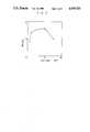
- FIG. 1 and FIG. 2show schematic illustrations of an embodiment of an electromagnetic device of the present invention at closed and open conditions respectively;
- FIG. 3, FIG. 4, FIG. 5 and FIG. 6show characteristic diagrams of an electromagnetic device of the present invention.
- FIG. 1 and FIG. 2show schematic illustrations of an electromagnetic device of an embodiment of the present invention at closed and open conditions respectively.
- numeral 1indicates a glass substrate
- numeral 2indicates a transparent electrode
- numeral 3indicates a solid of semisolid layer
- numeral 4indicates a micro-capsule
- numeral 5indicates a suspension
- numeral 6indicates a dispersing solvent.
- an anisotropic particleit is preferable as an anisotropic particle to employ needle like or planar particles having electrical and magnetical anisotropy.
- anisotropic particlesit is crucial to use such particles as having strong absorbing and reflecting ability for visible and near infrared region.
- the ratio of longitudinal axis to diameter (hereafter referred to as a) for needle like particlesis particularly significant, and the ratio of flat area to sectional area (hereafter referred to as a') for planar particles is particularly significant. Contrast between coloring and bleaching state is expressed by electrodichroic ratio (formula (1)).
- Dzoptical density at an aligned state by electric field or magnetic field.
- aaffects wavelength band causing spectra change, and the wavelength band decreases with the increase of a.
- anisotropic particleshave wide wavelength band where spectrum change occurs.
- a suitable range of ais determined in terms of the considerations of the magnitude of transmittance change and the width of the band where spectrum change occur.
- Preferable range of ais from 10 to 50.
- the rate and degree of orientation of anisotropic particlesincrease with the increase of strength of electric or magnetic field. Therefore, it is necessary to make the thickness of the solid or semisolid matrix as thin as possible under low strength of electric or magnetic field. It is preferable that anisotropic particles are controlled under low voltage in order to extend the life of the device. Actually, it is difficult to make the matrix layer of 50 ⁇ m because of the restriction of flatness of electrode.
- the diameter of micro-capsules dispersed in the matrix polymeris as small as possible in order to generate optically uniform change of color. From a practical point of view, it is preferable that the diameter of micro-capsules is not more than 25 ⁇ m, particularly not more than 5 ⁇ m.
- anisotropic particles employable in the present inventionare, for instance,
- Organic compounds particlessuch as haloalkaloid acid salt represented by helapathit (iodoquinine sulfate), deflection metal halide, deflection metal perhalide, nafoxidine hydrochloride and guanine,
- Inorganic compound grainssuch as basic carbonate lead, oxychloride bismuth, lead hydrogenarsenate, lead hydrogenphosphate, graphite, mica and garnet,
- Metal and metal oxide particlessuch as aluminium, chromium, gold, palladium, silver, tantalum, titanium, tin oxide, titanium oxide and vanadium pentoxide, and
- anisotropic particles having strong light-absorbing and light-reflecting ability for visible and near infrared regionsuch as needle like or planer metal, organometal such as hexacyano complex, tungsten bronze, Ti n O 2n-1 (1 ⁇ n ⁇ 2), and anisotropic particles at least coated with the above-mentioned material were particularly useful to improve the controllability of T G of DPS element.
- solventit is required of solvent that it disperses anisotropic particles uniformly and suspends the particles stably.
- at least the specific gravity of solventis near to that of anisotropic particle as much as possible.
- solventin order to improve the maximum value of transmittance of solar radiation on application of voltage, i.e., when anisotropic particles are aligned, solvent should be so selected as to make refractive index of anisotropic particles at alignment condition equals to that of the solid matrix.
- solventis, for instance, polydimethylsiloxane.
- the materials of the micro-capsules wherein the suspension are dispersedare polymeric materials such as polyester, polyamide, polyurethane, polyurea, polyvinyl alcohol, gelatin and epoxy resin, and inorganic materials such as silica, magnesium silicate, calcium silicate, strontium silicate and barium silicate.
- refractive index of suspension containing the anisotropic particles and swelling of the matrixare taken into consideration, and that a suitable combination thereof is used for the smart window.
- micro-capsuling methodinterfacial polymerization, IN SITU polymerization, direct dispersing method, coacervation method and the like can be adopted when anisotropic particles are made of polymeric materials. Further, micro-capsuling can be carried out by the following method:
- micro-capsulingcan also be carried out the following simplified method referred to as direct dispersing method:
- matrix polymeritself becomes substance of micro-capsules.
- interfacial reaction methodcan be adopted when substance involving micro-capsules is inorganic material.
- the matrix layer involving the encapsulated suspensionis sandwiched between a pair of electrodes at least one of which is a transparent electrode.
- a transparent electrodeLow electric resistance and high transmittance are required for the transparent electrode.
- ITO, SnO 2 , and ZnOcan be preferably used.
- semitransprent film of metalsuch as aluminium, platinum, gold, silver, copper and stainless steel, or semitransparent film of alloy thereof can be used as a transparent electrode.
- electrode-supporting substratei.e., glass, plastics and transparent ceramics can be adopted for the smart window of architecture, and plastics which is suitable for bending can be adopted for the smart window of vehicle.
- a reflecting indication devicecan be made by applying metal to one side of electrodes or substrate side.
- the size of the anisotropic particles used in the present inventionis different from that of ordinary liquid crystal.
- the size of the anisotropic particles used in the present invention which are made of inorganic material or organometalis between about 20-30 nm and about 20-30 ⁇ m.
- the anisotropic particleshave more shielding effect of light caused by light absorbing and reflecting ability depending on the shape factor than the ordinary liquid crystal.
- the shielding effect of light by reflectingcauses energy reflecting effect when the device using above-mentioned anisotropic particles are applied to windows, so that the load of cooling is lowered.
- anisotropic particles contained in micro capsulesare in a random orientation state, so that light is strongly absorbed or reflected by the anisotropic particles.
- the anisotropic particlesare orientated as follows:
- the anisotropic particlesare orientated in the way in which the major axes of anisotropic particles is parallel to the electric field.
- anisotropic particleeach having a planer shape, are orientated in the way in which planer faces of anisotropic particles is parallel to the electric field.
- the area having light absorbing or reflecting ability in the electromagnetic deviceis heavily lessened, and interaction between electric vector of polarized light and anisotropic particles is minimized, so that most of the light can be transmitted.
- one of the electrodes of the electromagnetic meanscomprises a pair of electrodes at least one of which being a transparent electrode.
- a surface of the anisotropic particlesis made of metal, metal oxide or organometal compound each having absorbing or reflecting ability for light of visible and near infrared region in order to improve the controllability of transmission. It is preferable to select metal or alloy from the group consisting of Pt, Pd, Au, Ag and Rh.
- metal or alloya mixed valence complex defined by the general formula of M 1x [M 2 (CN) 6 ] y , wherein M 1 and M 2 are transition metal, and x and y satisfy the relationships of 3 ⁇ n ⁇ 4 and 2 ⁇ y ⁇ 3 respectively.
- the metal or organometal compoundis deposited on the anisotropic particles by photodeposition method.
- metal oxideis tungsten bronze.
- the tungsten bronzeis deposited on the anisotropic particles by dipping anisotropic particles into electrolytically reduced acid solution of tungsten acid ions and aliphatic carboxylic acid ions.
- planar pearl mica particlesof which length was about 3 ⁇ m and aspect ratio was about 20, were added to 1 g of silicon oil.
- the silicon oilwas stirred enough to obtain uniform solution which showed glaze like pearl (hereafter referred to as solution A).
- solution A1.5 g of hexamethylenediisocyanate (HDI) was added to 10 g of trifunctional polyethylene glycol (3 PEG).
- solution B1 g of solution A was added to 10 g of solution B, and 0.5 weight % of tin octylic acid was added to them as catalyst, and then the solution was stirred heavily.
- the solutionbecame emulsion which generated many micro-drops of silicon oil containing pearl mica.
- Micro-spherical spacers of 50 ⁇ m diameterwere dispersed into the emulsive solution.
- the solutionwas spreaded on a glass substrate with transparent conductive film of SnO 2 .
- the other electrodewas put on the particle-suspend solution in such a manner that the solution was sandwiched between two glass substrates in order to make a cell.
- the 3 PEG and HDIwas completely condensated by heating the cell at 80° C. for 30 minutes, so that a cell could be solidified.
- the solidified cellshowed white glaze like pearl (closed condition shown in FIG. 1) when no-voltage way applied.
- voltageex. AC 100 V and 60 Hz
- Switching speed of solid cellwas as follows:
- the above examplewas an electro-optical device which can be controlled by electric field.
- a magnet-optical devicewhich is controlled by magnetic field, can also be fabricated in the same manner.
- a smart window of capsule typewas fabricated by the same method as described above, wherein the size of the window was 1 m ⁇ 1 m.
- a smart window of non-capsule typewas fabricated by sandwiching particle suspension comprising the same material and having the same density between glass substrates each coated with transparent conductive film, wherein the size of the window was 1 m ⁇ 1 m.
- the two smart windowswere arranged vertically for one month.
- the absorbance for lightwas measured at bottom and top of window for 400 nm wavelength light.
- the result of ratio of absorbance (bottom/top)is summarized in Table 1.
- the nonuniformity of density for particles in the solution in vertical conditioncan be caused by falling the particles due to the gravity. From the result of table 1, the above problem for nonuniformity is almost solved by the smart window of capsule type.
- the sampleswere stirred by a stirrer under radiation from light source of 400 W high voltage mercury-lamp.
- the radiation timewas changed one another as shown in Table 2.
- the particles in the solutionwere separated centrifugally to all samples, and the particles contained in each samples were cleaned enough with distilled water. Then the particles were dryed by heating at 120° C. for 20 hours.
- Amount of silver deposited on TOMwas analyzed by ICP method. The result is summarized in Table 2.
- the suspensionwere sandwiched between two glass substrates having a sheet resistance of 20 ⁇ / ⁇ coated with transparent conductive film to fabricate a cell.
- T GTransmittance of solar radiation
- ⁇ T GThe differences of transmittance before and after applying the voltage
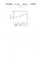
- FIG. 3shows the results of ⁇ T G (%) for each cells wherein five cells had different amount of silver deposition on TOM and one cell had no silver deposition on TOM.
- An abscissais the amount of silver deposition on TOM (weight %), and an ordinate is ⁇ T G (%).
- Dotsare measured values of ⁇ T G .
- ⁇ T Gincreases with the increase in the amount of silver deposition
- the value of ⁇ T G for 9.8 weight % of silver depositionshows 2.3 times larger than that of the sample with no silver deposition.
- Color tonewas white for TOM only, and the tone changed from gray to black-gray with the increase of the amount of silver deposition.
- Potassium tungstate, oxalic acidwere added into the water to obtain 500 ml solution having a pH value of 2.
- the added amount of potassium tungstate and oxalic acidwas 0.05 and 0.075 mol dm -3 respectively.
- the ratio of concentration of oxalic acid to potassium tangstateis 1.5.
- the solutionwas kept at 70° C. While sufficiently stirring the solution, the solution was electrolytically reduced for 4 hours by applying voltage with current density of 0.5 A /dm 2 between a pair of electrodes dipped therein, wherein the surface area of cathode was 60 cm 2 .
- the color tone of solutionchanged from achromatic transparency to blue green.
- T G of sandwich cellswere measured before and after applying voltage of AC 40 V and 60 Hz. ⁇ T G were calculated based on the measured values.
- FIG. 4shows ⁇ T G (%) for cells having different amount of tungsten bronze deposition on TOM.
- an abscissais the amount of tungsten bronze deposition (weight %) on TOM
- an ordinateis ⁇ T G (%)
- dotsshow measured values of ⁇ T G .
- TiOtitanium dioxide
- PSOpolydimethylcyclohexane
- a very small amount of beads having a mean diameter of 25 ⁇ mwere dispersed into the suspension. Then the suspension was sandwiched between two glass substrates, having a sheet resistance of 20 ⁇ / ⁇ , coated with transparent conductive to fabricate cells.
- T G of cellswere measured before and after applying voltage of AC 40 V and 60 Hz. ⁇ T G were calculated based on the measured values.
- FIG. 5shows the results of T G (%) for cells with different weight ratio of TiO/PSO.
- an abscissais the ratio of TiO/PSO (%)
- an ordinateis ⁇ T G (%)
- dotsshow measured values of ⁇ T G .
- ⁇ T Gincreases with the increase in weight ratio of TiO/PSO till the ratio of TiO/PSO becomes 10%. However, when the ratio exceeds 10%, ⁇ T G decreases. The maximum value of ⁇ T G is 16% when TiO/PSO is equal to 10%.
- ⁇ T Gwas about 4.5%.
- ⁇ T Greached about 3.6 times larger than that of no-reduced TOM.
- FIG. 6shows the spectra of transmittance from visible to near infrared region for samples 9 to 12. the transmittance in all region decreases with the increase in the density of particles. From this, TiO particle shows prominent absorbing ability for spectra of visible and near infrared region. Thus, it can be concluded that TiO particle might be the most suitable material for smart window.
- the time required for changing the direction of particlesis short, so that the present invention can be also applied to transmittable device and reflective device and the like.
Landscapes
- Physics & Mathematics (AREA)
- Nonlinear Science (AREA)
- General Physics & Mathematics (AREA)
- Optics & Photonics (AREA)
- Electrochromic Elements, Electrophoresis, Or Variable Reflection Or Absorption Elements (AREA)
Abstract
Description
The present invention relates to an electromagnetic device using a solid matrix layer wherein micro-capsules each containing suspension of anisotropic particles are dispersed, and more particularly to an electromagnetic device of large area applicable to a cell with the controllability of transmission, so-called smart window, permeation-type indication element. Reflection-type indication element and the like used for architecture and vehicles, wherein the transmittance or reflection of solar radiation of device are electrically controlled.
As a device using micro-capsules, there has been known a liquid crystal comprising micro-capsuled nematic liquid crystal (hereafter refereed to as NCAP). Further, it is considered that an electrochromic element (hereafter referred to as EC element) is useful for the smart window which enables to lessen the load of air-conditioner by electrically controlling the transmittance of solar radiation (hereafter referred to as TG) since the EC element changes the TG by electrochemical oxidation-reduction reaction of the electrochromic films (C. M. Lampert, Solar Energy Mater, 6 (1981) 1). In addition, as an element having controllability of the transmittance in the visible region, there has been provided by A. M. Marks an electromagnetic device comprising a suspension containing particles such as vanadium pentaoxide and lead carbonate, and electrodes sandwiching the suspension (hereafter referred to as DPS element) (U.S. Pat. No. 3,257,903 (1966)).
After that, the research of DPS elements has been performed and advanced by the group of Research Frontiers Inc.. The group reported that particles of hydrogenated herapathit were adaptable to DPS elements (U.S. Pat. No. 4,131,334(1977)).
NACP has a great advantage that a device having large area can be fabricated with maintaining high response rate of liquid crystal. In optical point of view, however, NACP has only switching function between transparent and milky (light scattering) states. Thus, NACP is applicable to a curtainless window and the like, but it is not applicable to the smart window requiring continuous control of TG. To the contrary, the EC element has controllability of transmission, but it has such disadvantage as its response speed becomes remarkably slow and uniform light control cannot be obtained when the area becomes large, since its controllability of transmission depends on electric current.
Further, the DPS element is liquid, so that it has optical nonuniformity caused by partial nonuniformity of thickness and particle density. The nonuniformity of thickness is caused by the falling of liquid due to the gravity when the DPS element is arranged in a vertical state assuming its use for windows. The nonuniformity of particle density in a vertical direction is caused by sedimentation of anisotropic particles (generally made of metal or metal oxide) due to the difference of specific gravity between the anisotropic particle and solvent. Further, it is difficult for DPS elements with the above-mentioned disadvantages to be applied to a smart window having a large area, since the nonuniformity of thickness and particle density are promoted with the increase of area of the element.
Still further, the conventional DPS elements hardly have the ability of absorbing and reflecting light of visible and near infrared region. The absorbed and reflected wavelength band is narrow even if such light is absorbed or reflected. As a result, the conventional DPS element is suitable only for curtainless windows, but not suitable enough for smart window because of the lack of controllability of TG.
To the contrary, the DPS element using hydrogenated herapathit has a good controllability of transmission, since it has strong light-absorbing ability for visible region. For the use of the window glass, however, DPS element has a problem in weatherproof ability since hydrogenated herapathit is organic compound.
It is accordingly an object of the present invention to solve the above-mentioned problem, i.e., to provide an electromagnetic device comprising solids or semisolids wherein micro-capsuled anisotropic particle suspension is contained, and a means for applying electric field or magnetic field to the anisotropic particles.
An electromagnetic device comprising solid matrix layer, wherein micro-capsuled suspension of anisotropic particles are contained, and a means for applying electric field or magnetic field to the anisotropic particles.
According to the present invention, as described hereinabove, not only the range of the control of transmittance of solar radiation can be much improved, but also a smart window of large scale can be realized by means of micro-capsuling, whereby nonuniformity of thickness between substrates, and nonuniformity of density of particles can be solved.
Further, the rate of orientation of particles remains high, so that the particles can be applied to transmissive device and reflective device of indicating.
In a preferred embodiment of the present invention, the electrodes of the electromagnetic means comprise a pair of electrodes at least one of which being a transparent electrode.
In another preferred embodiment of the present invention, a surface of the anisotropic particles is made of metal, metal oxide or organometal compound each having absorbing or reflecting ability for light of visible and near infrared region in order to improve the controllability of TG. It is preferable to select metal or alloy from the group consisting of Pt, Pd, Au, Ag and Rh. For organometal compound, a mixed valence complex defined by the general formula of M1x [M2 (CN)6 ]y, wherein M1 and M2 are transition metal, and x and y satisfy the relationships of 3≦x≦4 and 2≦y≦3 respectively. In the above embodiment, it is preferable that the metal or organometal compound is deposited on the anisotropic particles by the photodeposition method.
Further, it is preferable that metal oxide is tungsten bronze. The tungsten bronze is deposited on the anisotropic particles by immersing anisotropic particles into an electrolytically reduced acid solution containing therein tungsten acid ions and aliphatic carboxylic acid ions.
In still another preferred embodiment of the present invention, the surface of the anisotropic particles is covered with Tin O2n-1 where n satisfies the relationship of 1≦n≦2, preferably Tin O2n-1 is stabilized by the doping with a very small amount of nitrogen.
FIG. 1 and FIG. 2 show schematic illustrations of an embodiment of an electromagnetic device of the present invention at closed and open conditions respectively; and
FIG. 3, FIG. 4, FIG. 5 and FIG. 6 show characteristic diagrams of an electromagnetic device of the present invention.
Referring now to the drawing for more complete understanding of the present invention, there is explained an electromagnetic device.
FIG. 1 and FIG. 2 show schematic illustrations of an electromagnetic device of an embodiment of the present invention at closed and open conditions respectively. In the drawings,numeral 1 indicates a glass substrate,numeral 2 indicates a transparent electrode, numeral 3 indicates a solid of semisolid layer, numeral 4 indicates a micro-capsule,numeral 5 indicates a suspension, andnumeral 6 indicates a dispersing solvent.
In the present invention, it is preferable as an anisotropic particle to employ needle like or planar particles having electrical and magnetical anisotropy. In the case of applying anisotropic particles to the smart window, it is crucial to use such particles as having strong absorbing and reflecting ability for visible and near infrared region. Among parameters of particles having influence on the properties of the optical device, the ratio of longitudinal axis to diameter (hereafter referred to as a) for needle like particles is particularly significant, and the ratio of flat area to sectional area (hereafter referred to as a') for planar particles is particularly significant. Contrast between coloring and bleaching state is expressed by electrodichroic ratio (formula (1)).
grz=Dr/Dz (1)
where
Dr: optical density at a random orientation state
Dz: optical density at an aligned state by electric field or magnetic field.
Between grz and a there exists a relationship represented by formula (2). The contrast increases with the increase of a and a'.
grz∞a.sup.3 (2)
Further, a affects wavelength band causing spectra change, and the wavelength band decreases with the increase of a.
It is preferable for cell with the controllability of transmission that anisotropic particles have wide wavelength band where spectrum change occurs.
Thus, a suitable range of a is determined in terms of the considerations of the magnitude of transmittance change and the width of the band where spectrum change occur. Preferable range of a is from 10 to 50. The rate and degree of orientation of anisotropic particles increase with the increase of strength of electric or magnetic field. Therefore, it is necessary to make the thickness of the solid or semisolid matrix as thin as possible under low strength of electric or magnetic field. It is preferable that anisotropic particles are controlled under low voltage in order to extend the life of the device. Actually, it is difficult to make the matrix layer of 50 μm because of the restriction of flatness of electrode. Further, it is preferable that the diameter of micro-capsules dispersed in the matrix polymer is as small as possible in order to generate optically uniform change of color. From a practical point of view, it is preferable that the diameter of micro-capsules is not more than 25 μm, particularly not more than 5 μm.
Examples of anisotropic particles employable in the present invention are, for instance,
(1) Organic compounds particles such as haloalkaloid acid salt represented by helapathit (iodoquinine sulfate), deflection metal halide, deflection metal perhalide, nafoxidine hydrochloride and guanine,
(2) Inorganic compound grains such as basic carbonate lead, oxychloride bismuth, lead hydrogenarsenate, lead hydrogenphosphate, graphite, mica and garnet,
(3) Metal and metal oxide particles such as aluminium, chromium, gold, palladium, silver, tantalum, titanium, tin oxide, titanium oxide and vanadium pentoxide, and
(4) Particles covered with above-mentioned metal or metal oxide such as mica and glass flake.
Further, as a result of vigorous investigation, we inventors have found out that anisotropic particles having strong light-absorbing and light-reflecting ability for visible and near infrared region such as needle like or planer metal, organometal such as hexacyano complex, tungsten bronze, Tin O2n-1 (1≦n≦2), and anisotropic particles at least coated with the above-mentioned material were particularly useful to improve the controllability of TG of DPS element.
Diversity, refractive index, decomposition voltage, fluid point, boiling point, viscosity and the like are taken into consideration on selecting the kind of solvent.
First, it is required of solvent that it disperses anisotropic particles uniformly and suspends the particles stably. In order to satisfy the above requirements, at least the specific gravity of solvent is near to that of anisotropic particle as much as possible.
Second, in order to improve the maximum value of transmittance of solar radiation on application of voltage, i.e., when anisotropic particles are aligned, solvent should be so selected as to make refractive index of anisotropic particles at alignment condition equals to that of the solid matrix.
Third, in order to extend the life of electromagnetic device, it is necessary to select such solvent as having high decomposition voltage. Further in order to make effective electric field in the micro-capsule, it is preferable to use high-purified solvent including ionizable impurity as less as possible. In consideration of the application for the smart window, it is desired that fluid point is under minus 20° C., and that boiling point is over plus 80° C. Further, it is desired that viscosity of solvent is low since open-shut speed, particularly open-to-shut speed, of smart window depends on Brownian motion of the particles. Concrete example of solvent is, for instance, polydimethylsiloxane. As the materials of the micro-capsules wherein the suspension are dispersed, are polymeric materials such as polyester, polyamide, polyurethane, polyurea, polyvinyl alcohol, gelatin and epoxy resin, and inorganic materials such as silica, magnesium silicate, calcium silicate, strontium silicate and barium silicate.
On selecting the dispersing solvent, it is preferable that refractive index of suspension containing the anisotropic particles and swelling of the matrix are taken into consideration, and that a suitable combination thereof is used for the smart window.
For micro-capsuling method, interfacial polymerization, IN SITU polymerization, direct dispersing method, coacervation method and the like can be adopted when anisotropic particles are made of polymeric materials. Further, micro-capsuling can be carried out by the following method:
(1) To make a mixture of suspension containing anisotropic particles, substance involving micro-capsules and carrying medium forming latex.
(2) To apply the mixture onto a substrate.
(3) To remove only the carrying medium by drying.
Still further, micro-capsuling can also be carried out the following simplified method referred to as direct dispersing method:
(1) To add the suspension into a solution of polymeric material before the hardening.
(2) To stir the solution strongly to change the solution into emulsion.
(3) To harden the emulsion by heating, UV radiation and the like.
In the direct dispersing method, matrix polymer itself becomes substance of micro-capsules. Alternately, interfacial reaction method can be adopted when substance involving micro-capsules is inorganic material.
For the application to electro-optical device, the matrix layer involving the encapsulated suspension is sandwiched between a pair of electrodes at least one of which is a transparent electrode. Low electric resistance and high transmittance are required for the transparent electrode. From this point of view, ITO, SnO2, and ZnO can be preferably used. Further, when the electro-optical device are required to have strong shielding effect of light for near infrared region, semitransprent film of metal such as aluminium, platinum, gold, silver, copper and stainless steel, or semitransparent film of alloy thereof can be used as a transparent electrode.
The following materials can be used for electrode-supporting substrate, i.e., glass, plastics and transparent ceramics can be adopted for the smart window of architecture, and plastics which is suitable for bending can be adopted for the smart window of vehicle. Further, a reflecting indication device can be made by applying metal to one side of electrodes or substrate side.
The size of the anisotropic particles used in the present invention is different from that of ordinary liquid crystal. The size of the anisotropic particles used in the present invention which are made of inorganic material or organometal is between about 20-30 nm and about 20-30 μm. Thus, the anisotropic particles have more shielding effect of light caused by light absorbing and reflecting ability depending on the shape factor than the ordinary liquid crystal. The shielding effect of light by reflecting causes energy reflecting effect when the device using above-mentioned anisotropic particles are applied to windows, so that the load of cooling is lowered.
Referring now to an embodiment of the electromagnetic device of the present invention, comprising solid matrix layer containing encapsulated suspension of aniosotropic particles and a pair of electrodes which sandwiches the solid matrix layer, there is explained an operation of the present invention.
As shown in FIG. 1, when voltage is not applied between the electrodes, anisotropic particles contained in micro capsules are in a random orientation state, so that light is strongly absorbed or reflected by the anisotropic particles. By the application of voltage under suitable conditions, the anisotropic particles are orientated as follows:
(1) The anisotropic particles, each having a needle like shape, are orientated in the way in which the major axes of anisotropic particles is parallel to the electric field.
(2) The anisotropic particle, each having a planer shape, are orientated in the way in which planer faces of anisotropic particles is parallel to the electric field.
In result, the area having light absorbing or reflecting ability in the electromagnetic device is heavily lessened, and interaction between electric vector of polarized light and anisotropic particles is minimized, so that most of the light can be transmitted.
In a preferred embodiment of the present invention, one of the electrodes of the electromagnetic means comprises a pair of electrodes at least one of which being a transparent electrode.
In another preferred embodiment of the present invention, a surface of the anisotropic particles is made of metal, metal oxide or organometal compound each having absorbing or reflecting ability for light of visible and near infrared region in order to improve the controllability of transmission. It is preferable to select metal or alloy from the group consisting of Pt, Pd, Au, Ag and Rh. For organometal compound, a mixed valence complex defined by the general formula of M1x [M2 (CN)6 ]y, wherein M1 and M2 are transition metal, and x and y satisfy the relationships of 3≦n≦4 and 2≦y≦3 respectively. In the above embodiment, it is preferable that the metal or organometal compound is deposited on the anisotropic particles by photodeposition method.
Further, it is preferable that metal oxide is tungsten bronze. The tungsten bronze is deposited on the anisotropic particles by dipping anisotropic particles into electrolytically reduced acid solution of tungsten acid ions and aliphatic carboxylic acid ions.
Next there is explained a electromagnetic device of the present invention based on Examples. The scope of the present invention is not, however, limited to the examples.
0.1 g of planar pearl mica particles, of which length was about 3 μm and aspect ratio was about 20, were added to 1 g of silicon oil. The silicon oil was stirred enough to obtain uniform solution which showed glaze like pearl (hereafter referred to as solution A). 1.5 g of hexamethylenediisocyanate (HDI) was added to 10 g of trifunctional polyethylene glycol (3 PEG). The mixed solution was stirred enough to obtain uniform solution (hereafter referred to as solution B). 1 g of solution A was added to 10 g of solution B, and 0.5 weight % of tin octylic acid was added to them as catalyst, and then the solution was stirred heavily. The solution became emulsion which generated many micro-drops of silicon oil containing pearl mica. Micro-spherical spacers of 50 μm diameter were dispersed into the emulsive solution. The solution was spreaded on a glass substrate with transparent conductive film of SnO2. The other electrode was put on the particle-suspend solution in such a manner that the solution was sandwiched between two glass substrates in order to make a cell. The 3 PEG and HDI was completely condensated by heating the cell at 80° C. for 30 minutes, so that a cell could be solidified. The solidified cell showed white glaze like pearl (closed condition shown in FIG. 1) when no-voltage way applied. When voltage (ex.AC 100 V and 60 Hz) was applied to the cell, the color of the solid cell changed to transparence (open condition shown in FIG. 2). Switching speed of solid cell was as follows:
(1) The time required from closing to opening state for a cell was from several milliseconds to several tens of milliseconds.
(2) The time required from opening to closing state was several seconds.
There were no differences of properties of device after repeating the switching operations for several times. Thus, it was proved that the change of condition for closing and opening state was reversible.
The above example was an electro-optical device which can be controlled by electric field. Alternately, a magnet-optical device, which is controlled by magnetic field, can also be fabricated in the same manner.
A smart window of capsule type was fabricated by the same method as described above, wherein the size of the window was 1 m×1 m. A smart window of non-capsule type was fabricated by sandwiching particle suspension comprising the same material and having the same density between glass substrates each coated with transparent conductive film, wherein the size of the window was 1 m×1 m.
The two smart windows were arranged vertically for one month. The absorbance for light was measured at bottom and top of window for 400 nm wavelength light. The result of ratio of absorbance (bottom/top) is summarized in Table 1.
TABLE 1 ______________________________________ Ratio of absorbance for light Type (bottom/top) ______________________________________ capsule type 1.004 non-capsule type ∞ ______________________________________ where ∞ means that all particles suspended in the solution were sedimented.
The nonuniformity of density for particles in the solution in vertical condition can be caused by falling the particles due to the gravity. From the result of table 1, the above problem for nonuniformity is almost solved by the smart window of capsule type.
100 mg of planar mica particles covered with TiO2 (hereafter referred to as TOM), of which length was about 3 μm and aspect ratio was about 20, was added to 5 g of 1 wt % aqueous solution of silver nitrate. The solution was stirred enough to obtain suspension. The suspension was poured into a test tube and argon was bubbled in it for 15 min. Thereafter, the tests tube was shield. Five samples were prepared.
The samples were stirred by a stirrer under radiation from light source of 400 W high voltage mercury-lamp. The radiation time was changed one another as shown in Table 2.
The particles in the solution were separated centrifugally to all samples, and the particles contained in each samples were cleaned enough with distilled water. Then the particles were dryed by heating at 120° C. for 20 hours.
Amount of silver deposited on TOM was analyzed by ICP method. The result is summarized in Table 2.
TABLE 2 ______________________________________ Radiation time Ag Contents Sample No. (hour(s)) (weight %) ______________________________________ 1 0.5 0.4 2 2 0.68 3 3 2.18 4 4 3.71 5 5 9.8 ______________________________________
Two samples were made for comparing with the characteristics for TOM particles with and without silver deposition as follows. 50 mg of TOM particles with silver deposition and 50 mg of TOM particles with no silver deposition were added to 0.5 g of a solution of polydimethylcyclohexane respectively. Then each solutions were stirred enough to make uniform suspension.
A very small amount of beads of 25 μm in mean diameter, as a spacer, were dispersed into the suspension. The suspension were sandwiched between two glass substrates having a sheet resistance of 20 Ω/□ coated with transparent conductive film to fabricate a cell.
Transmittance of solar radiation (hereafter referred to as TG) of the sandwich cells were measured before and after applying the voltage ofAC 40 V and 60 Hz. The differences of transmittance before and after applying the voltage (hereinafter referred to as ΔTG) were calculated.
FIG. 3 shows the results of ΔTG (%) for each cells wherein five cells had different amount of silver deposition on TOM and one cell had no silver deposition on TOM. An abscissa is the amount of silver deposition on TOM (weight %), and an ordinate is ΔTG (%). Dots are measured values of ΔTG.
From FIG. 3, ΔTG increases with the increase in the amount of silver deposition, and the value of ΔTG for 9.8 weight % of silver deposition shows 2.3 times larger than that of the sample with no silver deposition. Color tone was white for TOM only, and the tone changed from gray to black-gray with the increase of the amount of silver deposition.
Potassium tungstate, oxalic acid were added into the water to obtain 500 ml solution having a pH value of 2. The added amount of potassium tungstate and oxalic acid was 0.05 and 0.075 mol dm-3 respectively. The ratio of concentration of oxalic acid to potassium tangstate is 1.5. The solution was kept at 70° C. While sufficiently stirring the solution, the solution was electrolytically reduced for 4 hours by applying voltage with current density of 0.5A /dm2 between a pair of electrodes dipped therein, wherein the surface area of cathode was 60 cm2. The color tone of solution changed from achromatic transparency to blue green.
10 ml of the above solution was poured into three test tubes respectively. Then 200 mg of TOM was added to them. The solutions with TOM were kept being stirred at 15° C. for prescribed period of time as shown in Table 3. Thereafter, TOM was centrifugally separated from each solutions, and separated TOM were purified with distilled water. They were dryed in vacuum for more than 20 hours at 50° C. The weight of tungsten bronze deposited on TOM was measured by ICP method. The result is summarized in Table 3.
TABLE 3 ______________________________________ Stirring time Tungsten bronze Sample No. (hour(s)) (weight %) ______________________________________ 6 1 7.6 7 2 10.4 8 3 14.1 ______________________________________
Next, 50 mg of fully dried TOM covered with tungsten bronze were added to 0.5 g of solution of polydimethylcyclohexane. The solution was stirred to obtain uniform suspension. A very small amount of beads having a mean diameter of 25 μm, as a spacer, were dispersed into the suspension. Then the suspension was sandwiched between two glass substrates, having a sheet resistance of 20 Ω/□ coated with transparent conductive film to fabricate a cell.
TG of sandwich cells were measured before and after applying voltage ofAC 40 V and 60 Hz. ΔTG were calculated based on the measured values.
FIG. 4 shows ΔTG (%) for cells having different amount of tungsten bronze deposition on TOM. In FIG. 4, an abscissa is the amount of tungsten bronze deposition (weight %) on TOM, an ordinate is ΔTG (%), and dots show measured values of ΔTG. In FIG. 4, the value of ΔTG for W=0 is substituted by value for TOM proposed by B. D. Bostwich et al (Japanese Unexamined Patent Publication No. 69308/1986.) It can be understood from FIG. 4 that ΔTG increases with the increase in the amount of tungsten bronze deposition, and that ΔTG for 14.1 weight % of tungsten bronze is 1.8 times larger than that of a sample with no tungsten bronze deposition.
200 mg TOM were reduced at 800° C. for 5 hours under nitrogen atmosphere with small amount of ammonia. After reduction, color of the TOM particle changed from white to black. The reduced black particles (TiO) were dispersed into polydimethylcyclohexane (PSO) to prepare four different suspensions. The weight ratio of TiO to PSO (TiO/PSO) are shown in Table 4.
TABLE 4 ______________________________________ TiO/PSO Sample No. (weight %/weight %) ______________________________________ 9 1% 10 2% 11 10% 12 15% ______________________________________
A very small amount of beads having a mean diameter of 25 μm were dispersed into the suspension. Then the suspension was sandwiched between two glass substrates, having a sheet resistance of 20 Ω/□, coated with transparent conductive to fabricate cells.
TG of cells were measured before and after applying voltage ofAC 40 V and 60 Hz. ΔTG were calculated based on the measured values.
FIG. 5 shows the results of TG (%) for cells with different weight ratio of TiO/PSO. In FIG. 5, an abscissa is the ratio of TiO/PSO (%), an ordinate is ΔTG (%), and dots show measured values of ΔTG. ΔTG increases with the increase in weight ratio of TiO/PSO till the ratio of TiO/PSO becomes 10%. However, when the ratio exceeds 10%, ΔTG decreases. The maximum value of ΔTG is 16% when TiO/PSO is equal to 10%.
For TOM proposed by B. D. Bostwick et al, ΔTG was about 4.5%. By reducing TOM, ΔTG reached about 3.6 times larger than that of no-reduced TOM.
FIG. 6 shows the spectra of transmittance from visible to near infrared region for samples 9 to 12. the transmittance in all region decreases with the increase in the density of particles. From this, TiO particle shows prominent absorbing ability for spectra of visible and near infrared region. Thus, it can be concluded that TiO particle might be the most suitable material for smart window.
According to the present invention, not only range of transmittance of solar radiation can be much improved, but also a smart window of large scale can be realized by means of micro-capsuling, whereby nonuniformity of thickness between substrates, and nonuniformity of density of particles can be solved.
In this device, the time required for changing the direction of particles is short, so that the present invention can be also applied to transmittable device and reflective device and the like.
Claims (4)
1. An electromagnetic device comprising:
(a) a solid matrix layer;
(b) micro-capsules containing a suspension of anisotropic particles being dispersed in the solid matrix layer;
(c) a means for applying an electric field or a magnetic field to the anisotropic particles, said means comprising a pair of electrodes, at least one of which is a transparent electrode; and
(d) the surface of the anisotropic particles being made of a mixed valence complex represented by the general formula of M1x [M2 (CN)6 ]y wherein M1 and M2 are at least one transition metal, and x and y satisfy the relationship of 3≦x≦4 and 2≦y≦3 respectively.
2. An electromagnetic device comprising:
(a) solid matrix layer;
(b) micro-capsules containing a suspension of anisotropic particles being dispersed in the solid matrix layer;
(c) a means for applying an electric field or a magnetic field to the anisotropic particles, said means comprising a pair of electrodes, at least one of which is a transparent electrode; and
(d) the surface of the anisotropic particles being made of a tungsten bronze.
3. An electromagnetic device comprising:
(a) a solid matrix layer;
(b) micro-capsules containing a suspension of anisotropic particles being dispersed in the solid matrix layer;
(c) a means for applying an electric field or a magnetic field to the anisotropic particles, said means, comprising a pair of electrodes, at least one of which is a transparent electrode; and
(d) the surface of the anisotropic particles being Tin O2n--1 where n satisfies the relationship of 1≦n≦2.
4. The electromagnetic device of claim 3, wherein the anisotropic particles of Tin O2n-1, where n satisfies the relationship of 1≦n≦2, are stabilized by the doping with a very small amount of nitrogen.
Applications Claiming Priority (8)
| Application Number | Priority Date | Filing Date | Title |
|---|---|---|---|
| JP62139450AJPS63303325A (en) | 1987-06-03 | 1987-06-03 | Electromagneto-optical device for optical element |
| JP62-139450 | 1987-06-03 | ||
| JP62195061AJPS6438732A (en) | 1987-08-04 | 1987-08-04 | Electromagneto-optical device |
| JP62-195061 | 1987-08-04 | ||
| JP62214643AJPS6457242A (en) | 1987-08-28 | 1987-08-28 | Electromagnetic optical device |
| JP62-214643 | 1987-08-28 | ||
| JP62284990AJPH01126629A (en) | 1987-11-11 | 1987-11-11 | Electromagnetic optical device |
| JP62-284990 | 1987-11-11 |
Publications (1)
| Publication Number | Publication Date |
|---|---|
| US4919521Atrue US4919521A (en) | 1990-04-24 |
Family
ID=27472224
Family Applications (1)
| Application Number | Title | Priority Date | Filing Date |
|---|---|---|---|
| US07/203,797Expired - LifetimeUS4919521A (en) | 1987-06-03 | 1988-06-02 | Electromagnetic device |
Country Status (1)
| Country | Link |
|---|---|
| US (1) | US4919521A (en) |
Cited By (120)
| Publication number | Priority date | Publication date | Assignee | Title |
|---|---|---|---|---|
| US5059003A (en)* | 1989-08-07 | 1991-10-22 | The United States Of America As Represented By The Secretary Of The Army | Fast optical switch and limiter using quantum size effect in metal grain composites |
| EP0488180A3 (en)* | 1990-11-28 | 1992-12-09 | Nippon Sheet Glass Co. Ltd. | Electrically responsive light controlling device |
| US5210637A (en)* | 1991-11-12 | 1993-05-11 | International Business Machines Corp. | High speed light modulation |
| EP0551138A1 (en)* | 1992-01-10 | 1993-07-14 | Hankuk Glass Industries, Inc. | Film for a light valve, and method for manufacturing the film |
| WO1994011772A1 (en)* | 1992-11-06 | 1994-05-26 | Research Frontiers Incorporated | Light modulating film of improved clarity for a light valve |
| DE4240821A1 (en)* | 1992-12-04 | 1994-06-09 | Merck Patent Gmbh | Novel electro-optical system for display devices etc. - comprising microporous material (e.g. zeolite or cyclo:dextran) with anisotropic, rod-shaped mols. fixed longitudinally in its pores |
| EP0615629A4 (en)* | 1991-11-01 | 1994-10-12 | Research Frontiers Inc | LIGHT VALVE WITH A FILM CONTAINING AN ENCAPPED LIQUID SUSPENSION AND PRODUCTION METHOD FOR THIS FILM. |
| US5409734A (en)* | 1992-01-10 | 1995-04-25 | Hankuk Glass Industries, Inc. | Making liquid suspension type light valve film |
| US5461506A (en)* | 1991-11-01 | 1995-10-24 | Research Frontiers Inc. | Light valve suspensions containing a trimellitate or trimesate and light valves containing the same |
| US5463491A (en)* | 1991-11-01 | 1995-10-31 | Research Frontiers Incorporated | Light valve employing a film comprising an encapsulated liquid suspension, and method of making such film |
| EP0679925A1 (en)* | 1993-03-09 | 1995-11-02 | Research Frontiers Incorporated | Light valve with low emissivity coating as electrode |
| US5467217A (en)* | 1991-11-01 | 1995-11-14 | Research Frontiers Incorporated | Light valve suspensions and films containing UV absorbers and light valves containing the same |
| WO1997002731A3 (en)* | 1996-06-29 | 1997-04-17 | Paolo Wolters | Flat elements for influencing visible electronic surfaces in window elements |
| US5677784A (en)* | 1995-07-24 | 1997-10-14 | Ellis D. Harris Sr. Family Trust | Array of pellicle optical gates |
| US5708525A (en)* | 1995-12-15 | 1998-01-13 | Xerox Corporation | Applications of a transmissive twisting ball display |
| US5717514A (en)* | 1995-12-15 | 1998-02-10 | Xerox Corporation | Polychromal segmented balls for a twisting ball display |
| US5717515A (en)* | 1995-12-15 | 1998-02-10 | Xerox Corporation | Canted electric fields for addressing a twisting ball display |
| US5728251A (en)* | 1995-09-27 | 1998-03-17 | Research Frontiers Inc | Light modulating film of improved UV stability for a light valve |
| US5737115A (en)* | 1995-12-15 | 1998-04-07 | Xerox Corporation | Additive color tristate light valve twisting ball display |
| US5739946A (en)* | 1995-09-21 | 1998-04-14 | Kabushiki Kaisha Toshiba | Display device |
| US5739801A (en)* | 1995-12-15 | 1998-04-14 | Xerox Corporation | Multithreshold addressing of a twisting ball display |
| US5751268A (en)* | 1995-12-15 | 1998-05-12 | Xerox Corporation | Pseudo-four color twisting ball display |
| US5751471A (en)* | 1997-05-02 | 1998-05-12 | Motorola, Inc. | Switchable lens and method of making |
| US5760761A (en)* | 1995-12-15 | 1998-06-02 | Xerox Corporation | Highlight color twisting ball display |
| US5767826A (en)* | 1995-12-15 | 1998-06-16 | Xerox Corporation | Subtractive color twisting ball display |
| US5777782A (en)* | 1996-12-24 | 1998-07-07 | Xerox Corporation | Auxiliary optics for a twisting ball display |
| WO1998019208A3 (en)* | 1996-10-25 | 1998-07-09 | Massachusetts Inst Technology | Nonemissive displays and piezoelectric power supplies therefor |
| US5892497A (en)* | 1995-12-15 | 1999-04-06 | Xerox Corporation | Additive color transmissive twisting ball display |
| US5900192A (en)* | 1998-01-09 | 1999-05-04 | Xerox Corporation | Method and apparatus for fabricating very small two-color balls for a twisting ball display |
| US5914805A (en)* | 1996-06-27 | 1999-06-22 | Xerox Corporation | Gyricon display with interstitially packed particles |
| WO1999039234A1 (en)* | 1998-01-30 | 1999-08-05 | Minnesota Mining And Manufacturing Company | Reflective particle display film and method of manufacture |
| US5961804A (en)* | 1997-03-18 | 1999-10-05 | Massachusetts Institute Of Technology | Microencapsulated electrophoretic display |
| US5976428A (en)* | 1998-01-09 | 1999-11-02 | Xerox Corporation | Method and apparatus for controlling formation of two-color balls for a twisting ball display |
| US5982346A (en)* | 1995-12-15 | 1999-11-09 | Xerox Corporation | Fabrication of a twisting ball display having two or more different kinds of balls |
| US5986629A (en)* | 1996-10-02 | 1999-11-16 | Xerox Corporation | Electrostatic discharge indicator |
| US6014247A (en)* | 1998-06-05 | 2000-01-11 | Lear Automotive Dearborn, Inc. | Electronic ink dimming mirror |
| US6017584A (en)* | 1995-07-20 | 2000-01-25 | E Ink Corporation | Multi-color electrophoretic displays and materials for making the same |
| AU717855B2 (en)* | 1992-11-06 | 2000-04-06 | Research Frontiers Incorporated | Light valve liquid suspension |
| US6067185A (en)* | 1997-08-28 | 2000-05-23 | E Ink Corporation | Process for creating an encapsulated electrophoretic display |
| US6120839A (en)* | 1995-07-20 | 2000-09-19 | E Ink Corporation | Electro-osmotic displays and materials for making the same |
| US6124851A (en)* | 1995-07-20 | 2000-09-26 | E Ink Corporation | Electronic book with multiple page displays |
| KR100287520B1 (en)* | 1994-05-09 | 2001-04-16 | 리서치 프론티어스 인코퍼레이티드 | Low emissivity coated light valves used as electrodes |
| US6241921B1 (en) | 1998-05-15 | 2001-06-05 | Massachusetts Institute Of Technology | Heterogeneous display elements and methods for their fabrication |
| US6249271B1 (en) | 1995-07-20 | 2001-06-19 | E Ink Corporation | Retroreflective electrophoretic displays and materials for making the same |
| US6262833B1 (en) | 1998-10-07 | 2001-07-17 | E Ink Corporation | Capsules for electrophoretic displays and methods for making the same |
| US6262706B1 (en) | 1995-07-20 | 2001-07-17 | E Ink Corporation | Retroreflective electrophoretic displays and materials for making the same |
| US6301040B1 (en)* | 2000-05-24 | 2001-10-09 | Research Frontiers Incorporated | SPD films having improved properties and light valves comprising same |
| US6348908B1 (en) | 1998-09-15 | 2002-02-19 | Xerox Corporation | Ambient energy powered display |
| US6376828B1 (en) | 1998-10-07 | 2002-04-23 | E Ink Corporation | Illumination system for nonemissive electronic displays |
| US6377387B1 (en) | 1999-04-06 | 2002-04-23 | E Ink Corporation | Methods for producing droplets for use in capsule-based electrophoretic displays |
| US6392786B1 (en) | 1999-07-01 | 2002-05-21 | E Ink Corporation | Electrophoretic medium provided with spacers |
| US6396205B1 (en) | 1998-12-18 | 2002-05-28 | Xerox Corporation | Nonspecular visual display and method |
| US6440252B1 (en) | 1999-12-17 | 2002-08-27 | Xerox Corporation | Method for rotatable element assembly |
| US6445489B1 (en) | 1998-03-18 | 2002-09-03 | E Ink Corporation | Electrophoretic displays and systems for addressing such displays |
| US6473072B1 (en) | 1998-05-12 | 2002-10-29 | E Ink Corporation | Microencapsulated electrophoretic electrostatically-addressed media for drawing device applications |
| US6480182B2 (en) | 1997-03-18 | 2002-11-12 | Massachusetts Institute Of Technology | Printable electronic display |
| US20020171910A1 (en)* | 2001-05-15 | 2002-11-21 | Pullen Anthony Edward | Electrophoretic displays containing magnetic particles |
| EP1267200A1 (en)* | 2001-06-12 | 2002-12-18 | Japan Capsular Products, Inc. | Magnetic display device |
| US6498114B1 (en) | 1999-04-09 | 2002-12-24 | E Ink Corporation | Method for forming a patterned semiconductor film |
| US6498674B1 (en) | 2000-04-14 | 2002-12-24 | Xerox Corporation | Rotating element sheet material with generalized containment structure |
| US6504525B1 (en) | 2000-05-03 | 2003-01-07 | Xerox Corporation | Rotating element sheet material with microstructured substrate and method of use |
| US6515649B1 (en)* | 1995-07-20 | 2003-02-04 | E Ink Corporation | Suspended particle displays and materials for making the same |
| US6518949B2 (en) | 1998-04-10 | 2003-02-11 | E Ink Corporation | Electronic displays using organic-based field effect transistors |
| US6524500B2 (en) | 2000-12-28 | 2003-02-25 | Xerox Corporation | Method for making microencapsulated gyricon beads |
| US6542284B2 (en)* | 2000-10-11 | 2003-04-01 | Canon Kabushiki Kaisha | Display device and manufacturing method therefor |
| US6545671B1 (en) | 2000-03-02 | 2003-04-08 | Xerox Corporation | Rotating element sheet material with reversible highlighting |
| US20030214697A1 (en)* | 2001-12-13 | 2003-11-20 | E Ink Corporation | Electrophoretic electronic displays with low-index films |
| US6665042B1 (en) | 2000-05-16 | 2003-12-16 | The University Of Rochester | Electrically switchable polymer liquid crystal and polymer birefringent flake in fluid host systems and optical devices utilizing same |
| EP1182430A3 (en)* | 2000-08-24 | 2004-01-02 | Siemens Aktiengesellschaft | Pointer type indicator |
| USD485294S1 (en) | 1998-07-22 | 2004-01-13 | E Ink Corporation | Electrode structure for an electronic display |
| US6677926B2 (en)* | 2001-06-11 | 2004-01-13 | Xerox Corporation | Electrophoretic display device |
| WO2004012002A1 (en)* | 2002-07-25 | 2004-02-05 | Luiz Antonio Herbst Junior | Adjustable electromagnetic waves filter |
| US6690350B2 (en)* | 2001-01-11 | 2004-02-10 | Xerox Corporation | Rotating element sheet material with dual vector field addressing |
| US6693620B1 (en) | 1999-05-03 | 2004-02-17 | E Ink Corporation | Threshold addressing of electrophoretic displays |
| US6699570B2 (en) | 2001-11-06 | 2004-03-02 | Xerox Corporation | Colored cyber toner using multicolored gyricon spheres |
| US6714340B2 (en)* | 2002-08-26 | 2004-03-30 | Michael D. Wright | Vehicle license plate cover |
| US6727881B1 (en)* | 1995-07-20 | 2004-04-27 | E Ink Corporation | Encapsulated electrophoretic displays and methods and materials for making the same |
| US20040189766A1 (en)* | 2000-08-17 | 2004-09-30 | Xerox Corporation | Electromagnetophoretic display system and method |
| US20040190114A1 (en)* | 1998-07-08 | 2004-09-30 | E Ink | Methods for achieving improved color in microencapsulated electrophoretic devices |
| US20040196226A1 (en)* | 2003-04-02 | 2004-10-07 | Kosc Tanya Z. | Optical devices having flakes with angularly dependent optical properties in response to an alternating current electric field when the flakes are suspended in a host fluid to provide a flake/fluid system which is conductive |
| US20040217929A1 (en)* | 1997-08-28 | 2004-11-04 | E Ink Corporation | Encapsulated electrophoretic displays having a monolayer of capsules and materials and methods for making the same |
| US20040233508A1 (en)* | 2003-05-20 | 2004-11-25 | Kosc Tanya Z. | Electrically addressable optical devices using a system of composite layered flakes suspended in a fluid host to obtain angularly dependent optical effects |
| US6839158B2 (en) | 1997-08-28 | 2005-01-04 | E Ink Corporation | Encapsulated electrophoretic displays having a monolayer of capsules and materials and methods for making the same |
| US6842657B1 (en) | 1999-04-09 | 2005-01-11 | E Ink Corporation | Reactive formation of dielectric layers and protection of organic layers in organic semiconductor device fabrication |
| US20050035941A1 (en)* | 1995-07-20 | 2005-02-17 | Albert Jonathan D. | Retroreflective electrophoretic displaya and materials for making the same |
| US6864875B2 (en) | 1998-04-10 | 2005-03-08 | E Ink Corporation | Full color reflective display with multichromatic sub-pixels |
| US6897848B2 (en) | 2001-01-11 | 2005-05-24 | Xerox Corporation | Rotating element sheet material and stylus with gradient field addressing |
| EP1410101A4 (en)* | 2001-04-25 | 2005-08-17 | Research Frontiers Inc | METALLIC PARTICLES OF ANISOMETRIC FORM, LIQUID SUSPENSIONS, FILM BASED ON SAID PARTICLES, AND LIGHT MODULATORS COMPRISING SAID PARTICLES |
| US20050213191A1 (en)* | 2004-03-23 | 2005-09-29 | E Ink Corporation | Light modulators |
| US6970154B2 (en) | 2001-01-11 | 2005-11-29 | Jpmorgan Chase Bank | Fringe-field filter for addressable displays |
| US7002728B2 (en) | 1997-08-28 | 2006-02-21 | E Ink Corporation | Electrophoretic particles, and processes for the production thereof |
| US7038655B2 (en) | 1999-05-03 | 2006-05-02 | E Ink Corporation | Electrophoretic ink composed of particles with field dependent mobilities |
| US7109968B2 (en) | 1995-07-20 | 2006-09-19 | E Ink Corporation | Non-spherical cavity electrophoretic displays and methods and materials for making the same |
| US7230750B2 (en) | 2001-05-15 | 2007-06-12 | E Ink Corporation | Electrophoretic media and processes for the production thereof |
| US7247379B2 (en) | 1997-08-28 | 2007-07-24 | E Ink Corporation | Electrophoretic particles, and processes for the production thereof |
| US7312916B2 (en) | 2002-08-07 | 2007-12-25 | E Ink Corporation | Electrophoretic media containing specularly reflective particles |
| US20080030832A1 (en)* | 2006-08-02 | 2008-02-07 | E Ink Corporation | Multi-layer light modulator |
| US20080150888A1 (en)* | 1995-07-20 | 2008-06-26 | E Ink Corporation | Electrostatically addressable electrophoretic display |
| US7411719B2 (en) | 1995-07-20 | 2008-08-12 | E Ink Corporation | Electrophoretic medium and process for the production thereof |
| US20090052007A1 (en)* | 2007-08-20 | 2009-02-26 | Samsung Electronics Co., Ltd. | Reflective magnetic display |
| US20090190198A1 (en)* | 2008-01-29 | 2009-07-30 | Young-Kuk Kwon | Film filter and flat panel display having the same |
| US20100148385A1 (en)* | 2001-05-15 | 2010-06-17 | E Ink Corporation | Electrophoretic media and processes for the production thereof |
| US20100283806A1 (en)* | 1997-08-28 | 2010-11-11 | E Ink Corporation | Multi-color electrophoretic displays and materials for making the same |
| US20100320481A1 (en)* | 2009-06-23 | 2010-12-23 | Sony Corporation | Organic electroluminescence device, display unit including the same, and method of manufacturing an organic electroluminescence device |
| EP2267523A2 (en) | 2004-07-12 | 2010-12-29 | Basf Se | Stabilized electrochromic media |
| US7956841B2 (en) | 1995-07-20 | 2011-06-07 | E Ink Corporation | Stylus-based addressing structures for displays |
| US20110193841A1 (en)* | 2002-06-13 | 2011-08-11 | E Ink Corporation | Methods for driving electrophoretic displays using dielectrophoretic forces |
| US7999787B2 (en) | 1995-07-20 | 2011-08-16 | E Ink Corporation | Methods for driving electrophoretic displays using dielectrophoretic forces |
| US8040594B2 (en) | 1997-08-28 | 2011-10-18 | E Ink Corporation | Multi-color electrophoretic displays |
| WO2011134582A1 (en) | 2010-04-28 | 2011-11-03 | Merck Patent Gmbh | Optical switch element comprising a liquid-crystalline medium |
| WO2011144299A1 (en) | 2010-05-19 | 2011-11-24 | Merck Patent Gmbh | Optical switch element comprising a liquid-crystalline medium |
| US8115729B2 (en) | 1999-05-03 | 2012-02-14 | E Ink Corporation | Electrophoretic display element with filler particles |
| EP2423294A1 (en) | 2010-08-24 | 2012-02-29 | Merck Patent GmbH | Switch element comprising a liquid-crystalline medium |
| DE102012006231A1 (en) | 2011-01-28 | 2012-08-02 | Merck Patent Gmbh | Layer arrangement for regulating the light transmission |
| US20130033741A1 (en)* | 2011-08-01 | 2013-02-07 | Hitachi Chemical Company, Ltd. | Suspended Particle Device, Light Control Device Using the Same, and Method for Driving the Same |
| WO2013056782A1 (en)* | 2011-10-20 | 2013-04-25 | Giesecke & Devrient Gmbh | Microcapsule and use thereof, security element having microcapsules and data carrier equipped therewith |
| US9005494B2 (en) | 2004-01-20 | 2015-04-14 | E Ink Corporation | Preparation of capsules |
| US10331005B2 (en) | 2002-10-16 | 2019-06-25 | E Ink Corporation | Electrophoretic displays |
| US11250794B2 (en) | 2004-07-27 | 2022-02-15 | E Ink Corporation | Methods for driving electrophoretic displays using dielectrophoretic forces |
| US11733580B2 (en) | 2010-05-21 | 2023-08-22 | E Ink Corporation | Method for driving two layer variable transmission display |
Citations (13)
| Publication number | Priority date | Publication date | Assignee | Title |
|---|---|---|---|---|
| US3257903A (en)* | 1960-11-21 | 1966-06-28 | Alvin M Marks | Electrically responsive light controlling devices employing suspended dipole particles and shear forces |
| GB1124678A (en)* | 1966-03-04 | 1968-08-21 | Alvin Melville Marks | Electrically responsive light controlling devices |
| US4126854A (en)* | 1976-05-05 | 1978-11-21 | Xerox Corporation | Twisting ball panel display |
| US4131334A (en)* | 1977-05-11 | 1978-12-26 | Research Frontiers Incorporated | Light polarizing materials, suspensions thereof, and process for manufacturing such suspensions |
| GB1586123A (en)* | 1977-05-19 | 1981-03-18 | Research Frontiers Inc | Light valves |
| US4298448A (en)* | 1979-02-02 | 1981-11-03 | Bbc Brown, Boveri & Company, Limited | Electrophoretic display |
| US4345820A (en)* | 1979-05-10 | 1982-08-24 | "L.C.C.-C.I.C.E. Compagnie Europeenne De Composants Electroniques" | Visual display apparatus for electrical signals recorded on a magnetic medium |
| US4407565A (en)* | 1981-01-16 | 1983-10-04 | Research Frontiers Incorporated | Light valve suspension containing fluorocarbon liquid |
| US4435047A (en)* | 1981-09-16 | 1984-03-06 | Manchester R & D Partnership | Encapsulated liquid crystal and method |
| US4442019A (en)* | 1978-05-26 | 1984-04-10 | Marks Alvin M | Electroordered dipole suspension |
| US4657349A (en)* | 1984-08-14 | 1987-04-14 | Temple University | Electro- and magneto-optic devices |
| US4663083A (en)* | 1978-05-26 | 1987-05-05 | Marks Alvin M | Electro-optical dipole suspension with reflective-absorptive-transmissive characteristics |
| US4680103A (en)* | 1986-01-24 | 1987-07-14 | Epid. Inc. | Positive particles in electrophoretic display device composition |
- 1988
- 1988-06-02USUS07/203,797patent/US4919521A/ennot_activeExpired - Lifetime
Patent Citations (13)
| Publication number | Priority date | Publication date | Assignee | Title |
|---|---|---|---|---|
| US3257903A (en)* | 1960-11-21 | 1966-06-28 | Alvin M Marks | Electrically responsive light controlling devices employing suspended dipole particles and shear forces |
| GB1124678A (en)* | 1966-03-04 | 1968-08-21 | Alvin Melville Marks | Electrically responsive light controlling devices |
| US4126854A (en)* | 1976-05-05 | 1978-11-21 | Xerox Corporation | Twisting ball panel display |
| US4131334A (en)* | 1977-05-11 | 1978-12-26 | Research Frontiers Incorporated | Light polarizing materials, suspensions thereof, and process for manufacturing such suspensions |
| GB1586123A (en)* | 1977-05-19 | 1981-03-18 | Research Frontiers Inc | Light valves |
| US4442019A (en)* | 1978-05-26 | 1984-04-10 | Marks Alvin M | Electroordered dipole suspension |
| US4663083A (en)* | 1978-05-26 | 1987-05-05 | Marks Alvin M | Electro-optical dipole suspension with reflective-absorptive-transmissive characteristics |
| US4298448A (en)* | 1979-02-02 | 1981-11-03 | Bbc Brown, Boveri & Company, Limited | Electrophoretic display |
| US4345820A (en)* | 1979-05-10 | 1982-08-24 | "L.C.C.-C.I.C.E. Compagnie Europeenne De Composants Electroniques" | Visual display apparatus for electrical signals recorded on a magnetic medium |
| US4407565A (en)* | 1981-01-16 | 1983-10-04 | Research Frontiers Incorporated | Light valve suspension containing fluorocarbon liquid |
| US4435047A (en)* | 1981-09-16 | 1984-03-06 | Manchester R & D Partnership | Encapsulated liquid crystal and method |
| US4657349A (en)* | 1984-08-14 | 1987-04-14 | Temple University | Electro- and magneto-optic devices |
| US4680103A (en)* | 1986-01-24 | 1987-07-14 | Epid. Inc. | Positive particles in electrophoretic display device composition |
Non-Patent Citations (4)
| Title |
|---|
| "Electrooptical Characteristics of Dipole Suspensions", Alvin M. Marks, Jul., 1969, vol. 8, No. 7, Applied Optics, pp. 1397-1412. |
| "Heat Mirror Coatings for Energy Conserving Windows", Carl M. Lampert, Solar Energy Materials 6, (1981), pp. 1-41. |
| Electrooptical Characteristics of Dipole Suspensions , Alvin M. Marks, Jul., 1969, vol. 8, No. 7, Applied Optics, pp. 1397 1412.* |
| Heat Mirror Coatings for Energy Conserving Windows , Carl M. Lampert, Solar Energy Materials 6, (1981), pp. 1 41.* |
Cited By (172)
| Publication number | Priority date | Publication date | Assignee | Title |
|---|---|---|---|---|
| US5059003A (en)* | 1989-08-07 | 1991-10-22 | The United States Of America As Represented By The Secretary Of The Army | Fast optical switch and limiter using quantum size effect in metal grain composites |
| EP0488180A3 (en)* | 1990-11-28 | 1992-12-09 | Nippon Sheet Glass Co. Ltd. | Electrically responsive light controlling device |
| US5204772A (en)* | 1990-11-28 | 1993-04-20 | Nippon Sheet Glass Co., Ltd. | Electrically responsive light controlling device |
| US5461506A (en)* | 1991-11-01 | 1995-10-24 | Research Frontiers Inc. | Light valve suspensions containing a trimellitate or trimesate and light valves containing the same |
| US5467217A (en)* | 1991-11-01 | 1995-11-14 | Research Frontiers Incorporated | Light valve suspensions and films containing UV absorbers and light valves containing the same |
| US5463492A (en)* | 1991-11-01 | 1995-10-31 | Research Frontiers Incorporated | Light modulating film of improved clarity for a light valve |
| EP0615629A4 (en)* | 1991-11-01 | 1994-10-12 | Research Frontiers Inc | LIGHT VALVE WITH A FILM CONTAINING AN ENCAPPED LIQUID SUSPENSION AND PRODUCTION METHOD FOR THIS FILM. |
| US5463491A (en)* | 1991-11-01 | 1995-10-31 | Research Frontiers Incorporated | Light valve employing a film comprising an encapsulated liquid suspension, and method of making such film |
| US5210637A (en)* | 1991-11-12 | 1993-05-11 | International Business Machines Corp. | High speed light modulation |
| US5409734A (en)* | 1992-01-10 | 1995-04-25 | Hankuk Glass Industries, Inc. | Making liquid suspension type light valve film |
| EP0551138A1 (en)* | 1992-01-10 | 1993-07-14 | Hankuk Glass Industries, Inc. | Film for a light valve, and method for manufacturing the film |
| AU717855B2 (en)* | 1992-11-06 | 2000-04-06 | Research Frontiers Incorporated | Light valve liquid suspension |
| WO1994011772A1 (en)* | 1992-11-06 | 1994-05-26 | Research Frontiers Incorporated | Light modulating film of improved clarity for a light valve |
| AU683629B2 (en)* | 1992-11-06 | 1997-11-20 | Research Frontiers Incorporated | Light modulating film of improved clarity for a light valve |
| DE4240821A1 (en)* | 1992-12-04 | 1994-06-09 | Merck Patent Gmbh | Novel electro-optical system for display devices etc. - comprising microporous material (e.g. zeolite or cyclo:dextran) with anisotropic, rod-shaped mols. fixed longitudinally in its pores |
| EP0679925A1 (en)* | 1993-03-09 | 1995-11-02 | Research Frontiers Incorporated | Light valve with low emissivity coating as electrode |
| KR100287520B1 (en)* | 1994-05-09 | 2001-04-16 | 리서치 프론티어스 인코퍼레이티드 | Low emissivity coated light valves used as electrodes |
| US20090040594A1 (en)* | 1995-07-20 | 2009-02-12 | E Ink Corporation | Multi-color electrophoretic displays and materials for making the same |
| US7791789B2 (en) | 1995-07-20 | 2010-09-07 | E Ink Corporation | Multi-color electrophoretic displays and materials for making the same |
| US8089453B2 (en) | 1995-07-20 | 2012-01-03 | E Ink Corporation | Stylus-based addressing structures for displays |
| US7999787B2 (en) | 1995-07-20 | 2011-08-16 | E Ink Corporation | Methods for driving electrophoretic displays using dielectrophoretic forces |
| US7956841B2 (en) | 1995-07-20 | 2011-06-07 | E Ink Corporation | Stylus-based addressing structures for displays |
| US7848007B2 (en) | 1995-07-20 | 2010-12-07 | E Ink Corporation | Electrophoretic medium and process for the production thereof |
| US8593718B2 (en) | 1995-07-20 | 2013-11-26 | E Ink Corporation | Electro-osmotic displays and materials for making the same |
| US6262706B1 (en) | 1995-07-20 | 2001-07-17 | E Ink Corporation | Retroreflective electrophoretic displays and materials for making the same |
| US7071913B2 (en) | 1995-07-20 | 2006-07-04 | E Ink Corporation | Retroreflective electrophoretic displays and materials for making the same |
| US6515649B1 (en)* | 1995-07-20 | 2003-02-04 | E Ink Corporation | Suspended particle displays and materials for making the same |
| US6249271B1 (en) | 1995-07-20 | 2001-06-19 | E Ink Corporation | Retroreflective electrophoretic displays and materials for making the same |
| US6017584A (en)* | 1995-07-20 | 2000-01-25 | E Ink Corporation | Multi-color electrophoretic displays and materials for making the same |
| US6124851A (en)* | 1995-07-20 | 2000-09-26 | E Ink Corporation | Electronic book with multiple page displays |
| US8384658B2 (en) | 1995-07-20 | 2013-02-26 | E Ink Corporation | Electrostatically addressable electrophoretic display |
| US7109968B2 (en) | 1995-07-20 | 2006-09-19 | E Ink Corporation | Non-spherical cavity electrophoretic displays and methods and materials for making the same |
| US20100207073A1 (en)* | 1995-07-20 | 2010-08-19 | E Ink Corporation | Electro-osmotic displays and materials for making the same |
| US6727881B1 (en)* | 1995-07-20 | 2004-04-27 | E Ink Corporation | Encapsulated electrophoretic displays and methods and materials for making the same |
| US20060245038A1 (en)* | 1995-07-20 | 2006-11-02 | E Ink Corporation | Non-spherical cavity electrophoretic displays and materials for making the same |
| US7391555B2 (en) | 1995-07-20 | 2008-06-24 | E Ink Corporation | Non-spherical cavity electrophoretic displays and materials for making the same |
| US20080150888A1 (en)* | 1995-07-20 | 2008-06-26 | E Ink Corporation | Electrostatically addressable electrophoretic display |
| US6680725B1 (en) | 1995-07-20 | 2004-01-20 | E Ink Corporation | Methods of manufacturing electronically addressable displays |
| US7746544B2 (en) | 1995-07-20 | 2010-06-29 | E Ink Corporation | Electro-osmotic displays and materials for making the same |
| US20050035941A1 (en)* | 1995-07-20 | 2005-02-17 | Albert Jonathan D. | Retroreflective electrophoretic displaya and materials for making the same |
| US7411719B2 (en) | 1995-07-20 | 2008-08-12 | E Ink Corporation | Electrophoretic medium and process for the production thereof |
| US20080211765A1 (en)* | 1995-07-20 | 2008-09-04 | E Ink Corporation | Stylus-based addressing structures for displays |
| US6120839A (en)* | 1995-07-20 | 2000-09-19 | E Ink Corporation | Electro-osmotic displays and materials for making the same |
| US5677784A (en)* | 1995-07-24 | 1997-10-14 | Ellis D. Harris Sr. Family Trust | Array of pellicle optical gates |
| US5739946A (en)* | 1995-09-21 | 1998-04-14 | Kabushiki Kaisha Toshiba | Display device |
| US5728251A (en)* | 1995-09-27 | 1998-03-17 | Research Frontiers Inc | Light modulating film of improved UV stability for a light valve |
| US5739801A (en)* | 1995-12-15 | 1998-04-14 | Xerox Corporation | Multithreshold addressing of a twisting ball display |
| US5892497A (en)* | 1995-12-15 | 1999-04-06 | Xerox Corporation | Additive color transmissive twisting ball display |
| US5767826A (en)* | 1995-12-15 | 1998-06-16 | Xerox Corporation | Subtractive color twisting ball display |
| US5760761A (en)* | 1995-12-15 | 1998-06-02 | Xerox Corporation | Highlight color twisting ball display |
| US5751268A (en)* | 1995-12-15 | 1998-05-12 | Xerox Corporation | Pseudo-four color twisting ball display |
| US5982346A (en)* | 1995-12-15 | 1999-11-09 | Xerox Corporation | Fabrication of a twisting ball display having two or more different kinds of balls |
| US5737115A (en)* | 1995-12-15 | 1998-04-07 | Xerox Corporation | Additive color tristate light valve twisting ball display |
| US5717514A (en)* | 1995-12-15 | 1998-02-10 | Xerox Corporation | Polychromal segmented balls for a twisting ball display |
| US5708525A (en)* | 1995-12-15 | 1998-01-13 | Xerox Corporation | Applications of a transmissive twisting ball display |
| US5717515A (en)* | 1995-12-15 | 1998-02-10 | Xerox Corporation | Canted electric fields for addressing a twisting ball display |
| US5914805A (en)* | 1996-06-27 | 1999-06-22 | Xerox Corporation | Gyricon display with interstitially packed particles |
| WO1997002731A3 (en)* | 1996-06-29 | 1997-04-17 | Paolo Wolters | Flat elements for influencing visible electronic surfaces in window elements |
| US5986629A (en)* | 1996-10-02 | 1999-11-16 | Xerox Corporation | Electrostatic discharge indicator |
| US6130773A (en)* | 1996-10-25 | 2000-10-10 | Massachusetts Institute Of Technology | Nonemissive displays and piezoelectric power supplies therefor |
| US5930026A (en)* | 1996-10-25 | 1999-07-27 | Massachusetts Institute Of Technology | Nonemissive displays and piezoelectric power supplies therefor |
| WO1998019208A3 (en)* | 1996-10-25 | 1998-07-09 | Massachusetts Inst Technology | Nonemissive displays and piezoelectric power supplies therefor |
| US5777782A (en)* | 1996-12-24 | 1998-07-07 | Xerox Corporation | Auxiliary optics for a twisting ball display |
| US5961804A (en)* | 1997-03-18 | 1999-10-05 | Massachusetts Institute Of Technology | Microencapsulated electrophoretic display |
| US6980196B1 (en) | 1997-03-18 | 2005-12-27 | Massachusetts Institute Of Technology | Printable electronic display |
| US6480182B2 (en) | 1997-03-18 | 2002-11-12 | Massachusetts Institute Of Technology | Printable electronic display |
| US5751471A (en)* | 1997-05-02 | 1998-05-12 | Motorola, Inc. | Switchable lens and method of making |
| US20040217929A1 (en)* | 1997-08-28 | 2004-11-04 | E Ink Corporation | Encapsulated electrophoretic displays having a monolayer of capsules and materials and methods for making the same |
| US7002728B2 (en) | 1997-08-28 | 2006-02-21 | E Ink Corporation | Electrophoretic particles, and processes for the production thereof |
| US8593721B2 (en) | 1997-08-28 | 2013-11-26 | E Ink Corporation | Multi-color electrophoretic displays and materials for making the same |
| US20100283806A1 (en)* | 1997-08-28 | 2010-11-11 | E Ink Corporation | Multi-color electrophoretic displays and materials for making the same |
| US9268191B2 (en) | 1997-08-28 | 2016-02-23 | E Ink Corporation | Multi-color electrophoretic displays |
| US8213076B2 (en) | 1997-08-28 | 2012-07-03 | E Ink Corporation | Multi-color electrophoretic displays and materials for making the same |
| US6392785B1 (en) | 1997-08-28 | 2002-05-21 | E Ink Corporation | Non-spherical cavity electrophoretic displays and materials for making the same |
| US7247379B2 (en) | 1997-08-28 | 2007-07-24 | E Ink Corporation | Electrophoretic particles, and processes for the production thereof |
| US8441714B2 (en) | 1997-08-28 | 2013-05-14 | E Ink Corporation | Multi-color electrophoretic displays |
| US8040594B2 (en) | 1997-08-28 | 2011-10-18 | E Ink Corporation | Multi-color electrophoretic displays |
| US6839158B2 (en) | 1997-08-28 | 2005-01-04 | E Ink Corporation | Encapsulated electrophoretic displays having a monolayer of capsules and materials and methods for making the same |
| US6067185A (en)* | 1997-08-28 | 2000-05-23 | E Ink Corporation | Process for creating an encapsulated electrophoretic display |
| US7242513B2 (en) | 1997-08-28 | 2007-07-10 | E Ink Corporation | Encapsulated electrophoretic displays having a monolayer of capsules and materials and methods for making the same |
| US5976428A (en)* | 1998-01-09 | 1999-11-02 | Xerox Corporation | Method and apparatus for controlling formation of two-color balls for a twisting ball display |
| US5900192A (en)* | 1998-01-09 | 1999-05-04 | Xerox Corporation | Method and apparatus for fabricating very small two-color balls for a twisting ball display |
| US6521145B1 (en) | 1998-01-30 | 2003-02-18 | 3M Innovative Properties Company | Reflective particle display film and method of manufacture |
| WO1999039233A1 (en)* | 1998-01-30 | 1999-08-05 | Minnesota Mining And Manufacturing Company | Reflective particle display film and method of manufacture |
| US6383619B1 (en) | 1998-01-30 | 2002-05-07 | 3M Innovative Properties Company | Reflective particle display film and method of manufacture |
| WO1999039234A1 (en)* | 1998-01-30 | 1999-08-05 | Minnesota Mining And Manufacturing Company | Reflective particle display film and method of manufacture |
| US6445489B1 (en) | 1998-03-18 | 2002-09-03 | E Ink Corporation | Electrophoretic displays and systems for addressing such displays |
| US7075502B1 (en) | 1998-04-10 | 2006-07-11 | E Ink Corporation | Full color reflective display with multichromatic sub-pixels |
| US6864875B2 (en) | 1998-04-10 | 2005-03-08 | E Ink Corporation | Full color reflective display with multichromatic sub-pixels |
| US8466852B2 (en) | 1998-04-10 | 2013-06-18 | E Ink Corporation | Full color reflective display with multichromatic sub-pixels |
| US6518949B2 (en) | 1998-04-10 | 2003-02-11 | E Ink Corporation | Electronic displays using organic-based field effect transistors |
| US6738050B2 (en) | 1998-05-12 | 2004-05-18 | E Ink Corporation | Microencapsulated electrophoretic electrostatically addressed media for drawing device applications |
| US6473072B1 (en) | 1998-05-12 | 2002-10-29 | E Ink Corporation | Microencapsulated electrophoretic electrostatically-addressed media for drawing device applications |
| US6241921B1 (en) | 1998-05-15 | 2001-06-05 | Massachusetts Institute Of Technology | Heterogeneous display elements and methods for their fabrication |
| US6014247A (en)* | 1998-06-05 | 2000-01-11 | Lear Automotive Dearborn, Inc. | Electronic ink dimming mirror |
| US20040190114A1 (en)* | 1998-07-08 | 2004-09-30 | E Ink | Methods for achieving improved color in microencapsulated electrophoretic devices |
| US9293511B2 (en) | 1998-07-08 | 2016-03-22 | E Ink Corporation | Methods for achieving improved color in microencapsulated electrophoretic devices |
| US7667684B2 (en) | 1998-07-08 | 2010-02-23 | E Ink Corporation | Methods for achieving improved color in microencapsulated electrophoretic devices |
| USD485294S1 (en) | 1998-07-22 | 2004-01-13 | E Ink Corporation | Electrode structure for an electronic display |
| US6348908B1 (en) | 1998-09-15 | 2002-02-19 | Xerox Corporation | Ambient energy powered display |
| US6376828B1 (en) | 1998-10-07 | 2002-04-23 | E Ink Corporation | Illumination system for nonemissive electronic displays |
| US6262833B1 (en) | 1998-10-07 | 2001-07-17 | E Ink Corporation | Capsules for electrophoretic displays and methods for making the same |
| US6396205B1 (en) | 1998-12-18 | 2002-05-28 | Xerox Corporation | Nonspecular visual display and method |
| US6377387B1 (en) | 1999-04-06 | 2002-04-23 | E Ink Corporation | Methods for producing droplets for use in capsule-based electrophoretic displays |
| US6842657B1 (en) | 1999-04-09 | 2005-01-11 | E Ink Corporation | Reactive formation of dielectric layers and protection of organic layers in organic semiconductor device fabrication |
| US6498114B1 (en) | 1999-04-09 | 2002-12-24 | E Ink Corporation | Method for forming a patterned semiconductor film |
| US8115729B2 (en) | 1999-05-03 | 2012-02-14 | E Ink Corporation | Electrophoretic display element with filler particles |
| US7038655B2 (en) | 1999-05-03 | 2006-05-02 | E Ink Corporation | Electrophoretic ink composed of particles with field dependent mobilities |
| US6693620B1 (en) | 1999-05-03 | 2004-02-17 | E Ink Corporation | Threshold addressing of electrophoretic displays |
| US6392786B1 (en) | 1999-07-01 | 2002-05-21 | E Ink Corporation | Electrophoretic medium provided with spacers |
| US6846377B2 (en) | 1999-12-17 | 2005-01-25 | Xerox Corporation | System and method for rotatable element assembly and laminate substrate assembly |
| US20020185216A1 (en)* | 1999-12-17 | 2002-12-12 | Xerox Corporation | System and method for rotatable element assembly and laminate substrate assembly |
| US6440252B1 (en) | 1999-12-17 | 2002-08-27 | Xerox Corporation | Method for rotatable element assembly |
| US6545671B1 (en) | 2000-03-02 | 2003-04-08 | Xerox Corporation | Rotating element sheet material with reversible highlighting |
| US6498674B1 (en) | 2000-04-14 | 2002-12-24 | Xerox Corporation | Rotating element sheet material with generalized containment structure |
| US6504525B1 (en) | 2000-05-03 | 2003-01-07 | Xerox Corporation | Rotating element sheet material with microstructured substrate and method of use |
| US6665042B1 (en) | 2000-05-16 | 2003-12-16 | The University Of Rochester | Electrically switchable polymer liquid crystal and polymer birefringent flake in fluid host systems and optical devices utilizing same |
| KR100815642B1 (en)* | 2000-05-24 | 2008-03-20 | 리서치 프론티어스 인코퍼레이티드 | SPD film having improved properties and light valve comprising the same |
| US6301040B1 (en)* | 2000-05-24 | 2001-10-09 | Research Frontiers Incorporated | SPD films having improved properties and light valves comprising same |
| WO2001090797A1 (en)* | 2000-05-24 | 2001-11-29 | Research Frontiers Incorporated | Spd films having improved properties and light valves comprising same |
| US20040189766A1 (en)* | 2000-08-17 | 2004-09-30 | Xerox Corporation | Electromagnetophoretic display system and method |
| US6847347B1 (en) | 2000-08-17 | 2005-01-25 | Xerox Corporation | Electromagnetophoretic display system and method |
| US6894677B2 (en) | 2000-08-17 | 2005-05-17 | Xerox Corporation | Electromagnetophoretic display system and method |
| EP1182430A3 (en)* | 2000-08-24 | 2004-01-02 | Siemens Aktiengesellschaft | Pointer type indicator |
| US6542284B2 (en)* | 2000-10-11 | 2003-04-01 | Canon Kabushiki Kaisha | Display device and manufacturing method therefor |
| US6524500B2 (en) | 2000-12-28 | 2003-02-25 | Xerox Corporation | Method for making microencapsulated gyricon beads |
| US6970154B2 (en) | 2001-01-11 | 2005-11-29 | Jpmorgan Chase Bank | Fringe-field filter for addressable displays |
| US6690350B2 (en)* | 2001-01-11 | 2004-02-10 | Xerox Corporation | Rotating element sheet material with dual vector field addressing |
| US6897848B2 (en) | 2001-01-11 | 2005-05-24 | Xerox Corporation | Rotating element sheet material and stylus with gradient field addressing |
| EP1410101A4 (en)* | 2001-04-25 | 2005-08-17 | Research Frontiers Inc | METALLIC PARTICLES OF ANISOMETRIC FORM, LIQUID SUSPENSIONS, FILM BASED ON SAID PARTICLES, AND LIGHT MODULATORS COMPRISING SAID PARTICLES |
| US6870661B2 (en) | 2001-05-15 | 2005-03-22 | E Ink Corporation | Electrophoretic displays containing magnetic particles |
| US7375875B2 (en) | 2001-05-15 | 2008-05-20 | E Ink Corporation | Electrophoretic media and processes for the production thereof |
| US7230750B2 (en) | 2001-05-15 | 2007-06-12 | E Ink Corporation | Electrophoretic media and processes for the production thereof |
| US20020171910A1 (en)* | 2001-05-15 | 2002-11-21 | Pullen Anthony Edward | Electrophoretic displays containing magnetic particles |
| US7532388B2 (en) | 2001-05-15 | 2009-05-12 | E Ink Corporation | Electrophoretic media and processes for the production thereof |
| US20100148385A1 (en)* | 2001-05-15 | 2010-06-17 | E Ink Corporation | Electrophoretic media and processes for the production thereof |
| US6677926B2 (en)* | 2001-06-11 | 2004-01-13 | Xerox Corporation | Electrophoretic display device |
| EP1267200A1 (en)* | 2001-06-12 | 2002-12-18 | Japan Capsular Products, Inc. | Magnetic display device |
| US6699570B2 (en) | 2001-11-06 | 2004-03-02 | Xerox Corporation | Colored cyber toner using multicolored gyricon spheres |
| US6865010B2 (en) | 2001-12-13 | 2005-03-08 | E Ink Corporation | Electrophoretic electronic displays with low-index films |
| US20030214697A1 (en)* | 2001-12-13 | 2003-11-20 | E Ink Corporation | Electrophoretic electronic displays with low-index films |
| US20110193841A1 (en)* | 2002-06-13 | 2011-08-11 | E Ink Corporation | Methods for driving electrophoretic displays using dielectrophoretic forces |
| WO2004012002A1 (en)* | 2002-07-25 | 2004-02-05 | Luiz Antonio Herbst Junior | Adjustable electromagnetic waves filter |
| US7312916B2 (en) | 2002-08-07 | 2007-12-25 | E Ink Corporation | Electrophoretic media containing specularly reflective particles |
| US6714340B2 (en)* | 2002-08-26 | 2004-03-30 | Michael D. Wright | Vehicle license plate cover |
| US10331005B2 (en) | 2002-10-16 | 2019-06-25 | E Ink Corporation | Electrophoretic displays |
| US20040196226A1 (en)* | 2003-04-02 | 2004-10-07 | Kosc Tanya Z. | Optical devices having flakes with angularly dependent optical properties in response to an alternating current electric field when the flakes are suspended in a host fluid to provide a flake/fluid system which is conductive |
| US7042617B2 (en) | 2003-04-02 | 2006-05-09 | The University Of Rochester | Optical devices having flakes suspended in a host fluid to provide a flake/fluid system providing flakes with angularly dependent optical properties in response to an alternating current electric field due to the dielectric properties of the system |
| US20040233508A1 (en)* | 2003-05-20 | 2004-11-25 | Kosc Tanya Z. | Electrically addressable optical devices using a system of composite layered flakes suspended in a fluid host to obtain angularly dependent optical effects |
| US6829075B1 (en) | 2003-05-20 | 2004-12-07 | The University Of Rochester | Electrically addressable optical devices using a system of composite layered flakes suspended in a fluid host to obtain angularly dependent optical effects |
| US9829764B2 (en) | 2003-12-05 | 2017-11-28 | E Ink Corporation | Multi-color electrophoretic displays |
| US9740076B2 (en) | 2003-12-05 | 2017-08-22 | E Ink Corporation | Multi-color electrophoretic displays |
| US9005494B2 (en) | 2004-01-20 | 2015-04-14 | E Ink Corporation | Preparation of capsules |
| US20050213191A1 (en)* | 2004-03-23 | 2005-09-29 | E Ink Corporation | Light modulators |
| US7327511B2 (en) | 2004-03-23 | 2008-02-05 | E Ink Corporation | Light modulators |
| EP2267523A2 (en) | 2004-07-12 | 2010-12-29 | Basf Se | Stabilized electrochromic media |
| US11250794B2 (en) | 2004-07-27 | 2022-02-15 | E Ink Corporation | Methods for driving electrophoretic displays using dielectrophoretic forces |
| US7492497B2 (en) | 2006-08-02 | 2009-02-17 | E Ink Corporation | Multi-layer light modulator |
| US20080030832A1 (en)* | 2006-08-02 | 2008-02-07 | E Ink Corporation | Multi-layer light modulator |
| US20090052007A1 (en)* | 2007-08-20 | 2009-02-26 | Samsung Electronics Co., Ltd. | Reflective magnetic display |
| US20090190198A1 (en)* | 2008-01-29 | 2009-07-30 | Young-Kuk Kwon | Film filter and flat panel display having the same |
| US8415658B2 (en)* | 2009-06-23 | 2013-04-09 | Sony Corporation | Organic electroluminescence device, display unit including the same, and method of manufacturing an organic electroluminescence device |
| US20100320481A1 (en)* | 2009-06-23 | 2010-12-23 | Sony Corporation | Organic electroluminescence device, display unit including the same, and method of manufacturing an organic electroluminescence device |
| WO2011134582A1 (en) | 2010-04-28 | 2011-11-03 | Merck Patent Gmbh | Optical switch element comprising a liquid-crystalline medium |
| WO2011144299A1 (en) | 2010-05-19 | 2011-11-24 | Merck Patent Gmbh | Optical switch element comprising a liquid-crystalline medium |
| US11733580B2 (en) | 2010-05-21 | 2023-08-22 | E Ink Corporation | Method for driving two layer variable transmission display |
| US12158684B2 (en) | 2010-05-21 | 2024-12-03 | E Ink Corporation | Method for driving two layer variable transmission display |
| EP2423294A1 (en) | 2010-08-24 | 2012-02-29 | Merck Patent GmbH | Switch element comprising a liquid-crystalline medium |
| WO2012100902A1 (en) | 2011-01-28 | 2012-08-02 | Merck Patent Gmbh | Layer arrangement for the regulation of light transmission |
| DE102012006231A1 (en) | 2011-01-28 | 2012-08-02 | Merck Patent Gmbh | Layer arrangement for regulating the light transmission |
| US20130033741A1 (en)* | 2011-08-01 | 2013-02-07 | Hitachi Chemical Company, Ltd. | Suspended Particle Device, Light Control Device Using the Same, and Method for Driving the Same |
| WO2013056782A1 (en)* | 2011-10-20 | 2013-04-25 | Giesecke & Devrient Gmbh | Microcapsule and use thereof, security element having microcapsules and data carrier equipped therewith |
Similar Documents
| Publication | Publication Date | Title |
|---|---|---|
| US4919521A (en) | Electromagnetic device | |
| US5293546A (en) | Oxide coated metal grid electrode structure in display devices | |
| US5138481A (en) | Electrochromic device with color gradient and method of making the device | |
| EP0363045B1 (en) | Electrochromic devices having a gradient of colour intensities | |
| DE3688218T2 (en) | Encapsulated liquid crystal with a smectic phase. | |
| US20030189749A1 (en) | Electrochromic-nanoparticle displays | |
| US4824222A (en) | Oxide bronze materials | |
| US5097358A (en) | Electrochromic element | |
| Kimura et al. | An improvement in the coloration properties of Ag deposition-based plasmonic EC devices by precise control of shape and density of deposited Ag nanoparticles | |
| Chang | Electrochromic and electrochemichromic materials and phenomena | |
| EP0551136A1 (en) | Light-polarizing materials, and method for manufacturing the materials | |
| US5204772A (en) | Electrically responsive light controlling device | |
| CA1111537A (en) | Electrochromic devices | |
| WO2018025939A1 (en) | Electrochromic element and electrochromic material | |
| US4746200A (en) | Electrochromic display device having white counter electrode | |
| US5111328A (en) | Electromagnetic radiation modulating device | |
| JP2586529B2 (en) | Liquid crystal display | |
| US7397594B2 (en) | Display element, display and method for manufacturing display | |
| Gambke et al. | Electrochromic layers for active optical filters | |
| JPS63303325A (en) | Electromagneto-optical device for optical element | |
| JP2003248242A (en) | Electrochromic device | |
| Cui et al. | All‐solid‐state complementary electrochromic windows based on the oxymethylene‐linked polyoxyethylene complexed with LiClO4 | |
| JPH0786621B2 (en) | Liquid crystal display | |
| JP2004191838A (en) | Electrochemical display device and its manufacturing method | |
| Nicoletta et al. | Electrochromism in switchable nematic emulsions |
Legal Events
| Date | Code | Title | Description |
|---|---|---|---|
| AS | Assignment | Owner name:NIPPON SHEET GLASS CO., LTD., 8, DOSHO-MACHI 4-CHO Free format text:ASSIGNMENT OF ASSIGNORS INTEREST.;ASSIGNORS:TADA, HIROAKI;YOSHIDA, HARUNOBU;KAWAHARA, HIDEO;AND OTHERS;REEL/FRAME:004894/0102 Effective date:19870524 Owner name:NIPPON SHEET GLASS CO., LTD., JAPAN Free format text:ASSIGNMENT OF ASSIGNORS INTEREST;ASSIGNORS:TADA, HIROAKI;YOSHIDA, HARUNOBU;KAWAHARA, HIDEO;AND OTHERS;REEL/FRAME:004894/0102 Effective date:19870524 | |
| FEPP | Fee payment procedure | Free format text:PAYOR NUMBER ASSIGNED (ORIGINAL EVENT CODE: ASPN); ENTITY STATUS OF PATENT OWNER: LARGE ENTITY | |
| STCF | Information on status: patent grant | Free format text:PATENTED CASE | |
| FPAY | Fee payment | Year of fee payment:4 | |
| FPAY | Fee payment | Year of fee payment:8 | |
| FPAY | Fee payment | Year of fee payment:12 |