US4919077A - Semiconductor producing apparatus - Google Patents
Semiconductor producing apparatusDownload PDFInfo
- Publication number
- US4919077A US4919077AUS07/247,443US24744388AUS4919077AUS 4919077 AUS4919077 AUS 4919077AUS 24744388 AUS24744388 AUS 24744388AUS 4919077 AUS4919077 AUS 4919077A
- Authority
- US
- United States
- Prior art keywords
- substrate
- chamber
- disposed
- electrodes
- film
- Prior art date
- Legal status (The legal status is an assumption and is not a legal conclusion. Google has not performed a legal analysis and makes no representation as to the accuracy of the status listed.)
- Expired - Fee Related
Links
Images


Classifications
- C—CHEMISTRY; METALLURGY
- C23—COATING METALLIC MATERIAL; COATING MATERIAL WITH METALLIC MATERIAL; CHEMICAL SURFACE TREATMENT; DIFFUSION TREATMENT OF METALLIC MATERIAL; COATING BY VACUUM EVAPORATION, BY SPUTTERING, BY ION IMPLANTATION OR BY CHEMICAL VAPOUR DEPOSITION, IN GENERAL; INHIBITING CORROSION OF METALLIC MATERIAL OR INCRUSTATION IN GENERAL
- C23C—COATING METALLIC MATERIAL; COATING MATERIAL WITH METALLIC MATERIAL; SURFACE TREATMENT OF METALLIC MATERIAL BY DIFFUSION INTO THE SURFACE, BY CHEMICAL CONVERSION OR SUBSTITUTION; COATING BY VACUUM EVAPORATION, BY SPUTTERING, BY ION IMPLANTATION OR BY CHEMICAL VAPOUR DEPOSITION, IN GENERAL
- C23C16/00—Chemical coating by decomposition of gaseous compounds, without leaving reaction products of surface material in the coating, i.e. chemical vapour deposition [CVD] processes
- C23C16/44—Chemical coating by decomposition of gaseous compounds, without leaving reaction products of surface material in the coating, i.e. chemical vapour deposition [CVD] processes characterised by the method of coating
- C23C16/50—Chemical coating by decomposition of gaseous compounds, without leaving reaction products of surface material in the coating, i.e. chemical vapour deposition [CVD] processes characterised by the method of coating using electric discharges
- C23C16/517—Chemical coating by decomposition of gaseous compounds, without leaving reaction products of surface material in the coating, i.e. chemical vapour deposition [CVD] processes characterised by the method of coating using electric discharges using a combination of discharges covered by two or more of groups C23C16/503 - C23C16/515
- C—CHEMISTRY; METALLURGY
- C23—COATING METALLIC MATERIAL; COATING MATERIAL WITH METALLIC MATERIAL; CHEMICAL SURFACE TREATMENT; DIFFUSION TREATMENT OF METALLIC MATERIAL; COATING BY VACUUM EVAPORATION, BY SPUTTERING, BY ION IMPLANTATION OR BY CHEMICAL VAPOUR DEPOSITION, IN GENERAL; INHIBITING CORROSION OF METALLIC MATERIAL OR INCRUSTATION IN GENERAL
- C23C—COATING METALLIC MATERIAL; COATING MATERIAL WITH METALLIC MATERIAL; SURFACE TREATMENT OF METALLIC MATERIAL BY DIFFUSION INTO THE SURFACE, BY CHEMICAL CONVERSION OR SUBSTITUTION; COATING BY VACUUM EVAPORATION, BY SPUTTERING, BY ION IMPLANTATION OR BY CHEMICAL VAPOUR DEPOSITION, IN GENERAL
- C23C16/00—Chemical coating by decomposition of gaseous compounds, without leaving reaction products of surface material in the coating, i.e. chemical vapour deposition [CVD] processes
- C23C16/44—Chemical coating by decomposition of gaseous compounds, without leaving reaction products of surface material in the coating, i.e. chemical vapour deposition [CVD] processes characterised by the method of coating
- C23C16/448—Chemical coating by decomposition of gaseous compounds, without leaving reaction products of surface material in the coating, i.e. chemical vapour deposition [CVD] processes characterised by the method of coating characterised by the method used for generating reactive gas streams, e.g. by evaporation or sublimation of precursor materials
- C23C16/452—Chemical coating by decomposition of gaseous compounds, without leaving reaction products of surface material in the coating, i.e. chemical vapour deposition [CVD] processes characterised by the method of coating characterised by the method used for generating reactive gas streams, e.g. by evaporation or sublimation of precursor materials by activating reactive gas streams before their introduction into the reaction chamber, e.g. by ionisation or addition of reactive species
- C—CHEMISTRY; METALLURGY
- C23—COATING METALLIC MATERIAL; COATING MATERIAL WITH METALLIC MATERIAL; CHEMICAL SURFACE TREATMENT; DIFFUSION TREATMENT OF METALLIC MATERIAL; COATING BY VACUUM EVAPORATION, BY SPUTTERING, BY ION IMPLANTATION OR BY CHEMICAL VAPOUR DEPOSITION, IN GENERAL; INHIBITING CORROSION OF METALLIC MATERIAL OR INCRUSTATION IN GENERAL
- C23C—COATING METALLIC MATERIAL; COATING MATERIAL WITH METALLIC MATERIAL; SURFACE TREATMENT OF METALLIC MATERIAL BY DIFFUSION INTO THE SURFACE, BY CHEMICAL CONVERSION OR SUBSTITUTION; COATING BY VACUUM EVAPORATION, BY SPUTTERING, BY ION IMPLANTATION OR BY CHEMICAL VAPOUR DEPOSITION, IN GENERAL
- C23C16/00—Chemical coating by decomposition of gaseous compounds, without leaving reaction products of surface material in the coating, i.e. chemical vapour deposition [CVD] processes
- C23C16/44—Chemical coating by decomposition of gaseous compounds, without leaving reaction products of surface material in the coating, i.e. chemical vapour deposition [CVD] processes characterised by the method of coating
- C23C16/48—Chemical coating by decomposition of gaseous compounds, without leaving reaction products of surface material in the coating, i.e. chemical vapour deposition [CVD] processes characterised by the method of coating by irradiation, e.g. photolysis, radiolysis, particle radiation
- C23C16/482—Chemical coating by decomposition of gaseous compounds, without leaving reaction products of surface material in the coating, i.e. chemical vapour deposition [CVD] processes characterised by the method of coating by irradiation, e.g. photolysis, radiolysis, particle radiation using incoherent light, UV to IR, e.g. lamps
- C—CHEMISTRY; METALLURGY
- C23—COATING METALLIC MATERIAL; COATING MATERIAL WITH METALLIC MATERIAL; CHEMICAL SURFACE TREATMENT; DIFFUSION TREATMENT OF METALLIC MATERIAL; COATING BY VACUUM EVAPORATION, BY SPUTTERING, BY ION IMPLANTATION OR BY CHEMICAL VAPOUR DEPOSITION, IN GENERAL; INHIBITING CORROSION OF METALLIC MATERIAL OR INCRUSTATION IN GENERAL
- C23C—COATING METALLIC MATERIAL; COATING MATERIAL WITH METALLIC MATERIAL; SURFACE TREATMENT OF METALLIC MATERIAL BY DIFFUSION INTO THE SURFACE, BY CHEMICAL CONVERSION OR SUBSTITUTION; COATING BY VACUUM EVAPORATION, BY SPUTTERING, BY ION IMPLANTATION OR BY CHEMICAL VAPOUR DEPOSITION, IN GENERAL
- C23C16/00—Chemical coating by decomposition of gaseous compounds, without leaving reaction products of surface material in the coating, i.e. chemical vapour deposition [CVD] processes
- C23C16/44—Chemical coating by decomposition of gaseous compounds, without leaving reaction products of surface material in the coating, i.e. chemical vapour deposition [CVD] processes characterised by the method of coating
- C23C16/48—Chemical coating by decomposition of gaseous compounds, without leaving reaction products of surface material in the coating, i.e. chemical vapour deposition [CVD] processes characterised by the method of coating by irradiation, e.g. photolysis, radiolysis, particle radiation
- C23C16/483—Chemical coating by decomposition of gaseous compounds, without leaving reaction products of surface material in the coating, i.e. chemical vapour deposition [CVD] processes characterised by the method of coating by irradiation, e.g. photolysis, radiolysis, particle radiation using coherent light, UV to IR, e.g. lasers
Definitions
- the present inventionrelates to a semiconductor producing apparatus, and more particularly to a photochemical vapor deposition apparatus for forming a chemical vapor deposited film on a heated substrate by subjecting a reaction gas supplied into a reaction chamber to decomposition by the energy of light applied thereto through a light transmissive window from the outside of the reaction chamber.
- photochemical vapor deposition(chemical vapor deposition, which will be referred to as CVD hereafter)
- light energysuch as a laser beam and an ultraviolet light is used as an energy source for CVD.
- An excimer laser or a carbon dioxide gas laseris generally employed as the laser, while a low-pressure mercury lamp, a high-pressure mercury lamp, or a deuterium lamp is used as an ultraviolet light source.
- FIG. 4is a cross-sectional view schematically illustrating a conventional optical CVD apparatus which is applied to the above-described method, as disclosed in, for instance, Japanese Patent Laid-Open No. 152023/1985.
- the conventional optical CVD apparatuscomprises the following components or substances: a reaction vessel 1 constituting a reaction chamber la; a substrate 2 on which a film is formed; a fixing base 3 for mounting the substrate thereon; a heater 4 for heating the substrate on the fixing base 3; a reaction gas 5 such as a silane gas; a post-reaction gas 6; a reaction gas supplying port 7; a gas discharge port 8; light transmissive windows 9 formed of a light transmissive material; a carbon dioxide gas laser oscillator 10; an optical system 11 for reducing the diameter of a carbon dioxide gas laser beam; a carbon dioxide gas laser beam 12 generated by the laser oscillator 10 and used to excite and decompose the reaction gas; and a damper 13 for absorbing the carbon dioxide gas laser beam which has passed through
- the silane gas 5when the silane gas 5 is supplied from the supply port 7 to the reaction chamber 1a, the silane gas 5 is excited and decomposed by the carbon dioxide gas laser beam 12 which enters through the transmissive window 9 after it is generated by the carbon dioxide gas laser oscillator 10 and its beam diameter is then reduced by the optical system 11.
- the reason for thisis that resonance absorption takes place at a wavelength of 10.59 ⁇ m of the carbon dioxide gas laser.
- a reaction product obtained as a resultis deposited on the substrate 2 heated to a low temperature by the heater 4, and an amorphous silicon film is formed on the substrate 2.
- the post-reaction gas 6is discharged through the discharge port 8.
- the carbon dioxide gas laser beam 12 which has passed through the reaction chamber 1ais absorbed by the damper 13.
- the conventional semiconductor producing apparatusit is possible to form an amorphous silicon film on a substrate by decomposing the silane gas by the carbon dioxide gas laser beam, as described above.
- the type of film formedis disadvantageously restricted to the amorphous silicon film, and it is difficult to form a silicon oxide film or a silicon nitride film by using the above-described apparatus since oxygen, nitrogen suboxide, nitrogen, or ammonia which is supplied by being added to the silane gas is difficult to decompose by the carbon dioxide gas laser.
- Another object of the present inventionis to provide a semiconductor producing apparatus which is capable of controlling a film forming speed during film formation, thereby making it possible to obtain a uniform distribution of film thickness during film formation.
- Still another object of the present inventionis to provide a semiconductor producing apparatus which is capable of rendering active the surface of a substrate and a film surface on which active species are deposited consecutively during film formation, thereby making it possible to form a dense film on the substrate.
- a semiconductor producing apparatusis provided with an introduction gas supplying port being separate from a reaction supplying port, and the introduction gas is introduced into a reaction chamber after being converted into a plasma state.
- the introduction gasis introduced into a reaction chamber after being converted into a plasma state.
- oxygen or nitrogen suboxideafter being converted into a plasma state, is introduced through the introduction gas supplying port into the reaction chamber and undergoes reaction with silane decomposed by the carbon dioxide gas laser, it is possible to form a silicon dioxide film at a low temperature.
- nitrogen or ammonia converted into a plasma stateis introduced, it becomes possible to form a silicon nitride film at a low temperature.
- a semiconductor producing apparatusis provided with two kinds of electrodes disposed in upper and lower positions, respectively, in a reaction vessel opposing each other, the upper one of the electrodes being either a single electrode connected to a high-frequency power source or by a plurality of electrodes each connected to a high-frequency power source, and the lower electrode being a common electrode on which a substrate for forming a film is mounted. Accordingly, by establishing voltages to be applied to the electrodes at the time of forming a film on the substrate, it becomes possible to control the film forming speed.
- a semiconductor producing apparatusis provided with an ultraviolet light source disposed adjacent to a reaction vessel and for irradiating the inside of the reaction vessel; and two kinds of electrodes disposed in upper and lower positions, respectively, in the reaction vessel opposing each other, the upper one of the electrodes being either a single mesh electrode connected to a high frequency power source or a plurality of mesh electrodes each connected to a high-frequency power source, and the lower electrode being a common electrode on which a substrate for forming a film is mounted.
- FIG. 1is a cross-sectional view of a semiconductor producing apparatus in accordance with an embodiment of the present invention
- FIG. 2is a cross-sectional view of a semiconductor producing apparatus in accordance with another embodiment of the present invention.
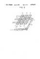
- FIG. 3is a perspective view of electrodes according to still another embodiment of the present invention.
- FIG. 4is a cross-sectional view illustrating a conventional semiconductor producing apparatus.
- FIG. 1is a cross-sectional view schematically illustrating a semiconductor producing apparatus in accordance with an embodiment of the present invention.
- numerals 1 to 13denote the same components or substances as those shown in FIG. 4.
- reference numeral 1denotes the reaction vessel forming the reaction chamber 1a and having on opposite sides thereof windows 9 through which the carbon dioxide gas laser beam 12 is transmitted.
- the reaction gas supplying port 7, which is open in the direction perpendicular to the axial direction of the carbon dioxide gas laser beam 12,is provided at an upper portion of the reaction vessel 1.
- the silane gas 5which serves as a first reaction gas is supplied through the gas supplying port 7.
- a gas introducing port 14is also provided at the upper portion of the reaction vessel 1, and an introduction gas 15, which serves as a second reaction gas converted into a plasma state by a microwave oscillator 18, is introduced through the gas introducing port 14.
- the introduction gas 15is oxygen or nitrogen suboxide when a silicon oxide film is formed; nitrogen or ammonia when a silicon nitride film is formed; or argon when an amorphous silicon film is formed at high speed.
- Numeral 16denotes a plasma generating furnace; 17, a waveguide including a matching device, a directional coupler, a converting waveguide, etc.; 18, a microwave oscillator; and 19, a plasma generating pipe comprising a quartz pipe.
- the plasma generating pipe 19is connected to the reaction chamber 1a via a port or a metal adapter and is used to supply into the reaction chamber 1a the introduction gas converted into a plasma state by microwaves.
- oxygen or nitrogen suboxide 15is supplied into the plasma generating pipe 19, and is introduced into the reaction chamber 1a after being converted into a plasma state upon excitation by the microwaves.
- This excited oxygen or nitrogen suboxideis introduced through the reaction gas supplying port 7 and reacts with silane 5 decomposed by the carbon dioxide gas laser beam 12, forming a silicon oxide film on the substrate 2.
- nitrogen or ammonia 15is supplied into the plasma generating pipe 19, and is introduced into the reaction chamber 1a after being converted into a plasma state upon excitation by the microwaves.
- This excited nitrogen or ammoniais introduced through the reaction gas supplying port 7 and reacts with silane 5 decomposed by the carbon dioxide gas laser beam 12, forming a silicon nitride film on the substrate 2.
- argon 15is supplied into the plasma generating pipe 19, and is introduced into the reaction chamber 1a after being converted into a plasma state upon excitation by the microwaves.
- This excited argoncollides with silane 5 in the reaction chamber 1a and decomposes the silane 5, and it is thus possible to form an amorphous silicon film on the substrate 2, coupled with the decomposing action of the silane 5 by the carbon dioxide gas laser beam 12.
- silaneis used as the reaction gas in the above-described embodiment, disilane, trisilane or the like may be used instead of silane.
- the arrangementis provided such that an introduction gas supplying port is provided separately from a reaction gas supplying port, and the introduction gas is introduced into a reaction chamber after being converted into a plasma state, and a thin film is formed on a substrate by means of the reaction gas excited and decomposed by the laser beam and the introduction gas converted into a plasma state. Therefore, there is the advantage that it is possible to provide a semiconductor producing apparatus which is capable of forming a silicon oxide film and a silicon nitride film at a low temperature and of forming an amorphous silicon film at a high speed and at a low temperature.
- the structureis such that the gas supplying port 17, the gas introducing port 14, and the beam incidence window 9 are located on one side of the substrate 2, there is a possibility that the film forming speed may become locally high, resulting in variations in the film thickness.
- the fact that the beam incidence window 9, the gas supplying port 7, and the gas introducing port 14 are located on one side of the substrate 2means that the power density may become high in the vicinity of those parts of the apparatus, with the result that the exciting energy may become high and the molecular density of the gas involved in the reaction for the film formation may become high.
- a semiconductor producing apparatus in accordance with another embodiment of the present invention, shown in FIG. 2,is capable of obtaining a uniform distribution of the film thickness by controlling the film forming speed in order to overcome the above-described problem of the apparatus shown in FIG. 1.
- reference numeral 21denotes a reaction vessel constituting a reaction chamber 21a and provided with a beam incidence window 23 and a beam emergence window 24 through both of which a carbon dioxide gas laser beam 22 is transmitted.
- a heater 27for heating a substrate 26 disposed on a mounting base 25 and serving as a lower common electrode connected to ground.
- a gas supplying port 28 and a gas introducing port 29both having openings oriented in the same direction as the axial direction of the carbon dioxide gas laser beam 22.
- the silane gas, disilane gas, or trisilane gaswhich serves as the first reaction gas is supplied into the reaction vessel 21 through the gas supplying port 28.
- Reference numeral 31denotes a window through which ultraviolet rays are transmitted, the window 31 being disposed on the reaction vessel 21 above the mounting base 25.
- Numeral 32denotes an ultraviolet light source such as a low-pressure mercury lamp or the like, which is provided adjacent to the reaction vessel 21 for irradiating the inside of the vessel 21 with ultraviolet rays.
- Numerals 33 to 35denote upper electrodes disposed inside the reaction vessel 21 along the direction of propagation of the laser beam opposing a mounting surface 25a of the mounting base 25, the electrodes 33-35 being respectively connected to high-frequency power sources 36-38.
- the electrodes 33-35are mesh electrodes which are obtained by etching stainless steel thin plates (not shown) to obtain a transmittance of 90% or more.
- Numeral 39denotes a carbon dioxide gas laser oscillator for issuing the carbon dioxide gas laser beam 22.
- the carbon dioxide gas laser oscillator 39is disposed outside the reaction vessel 21 exciting and decomposing the first reaction gas during film formation.
- numeral 40denotes a plasma generating pipe; 41 denotes a plasma generating furnace; 42 denotes a waveguide; 43 and 44 denote feed throughs for introducing electric currents to electrodes 33, 34, and 35 and mounting base 25.
- arrows P, Q and R in the drawingindicate the directions of gas flow.
- the film forming speedcan be controlled, even if the beam incidence window 23 of the carbon dioxide gas laser beam 22, the gas supplying port 28, and the gas introducing port 29 are disposed on one side of the substrate 26, the film forming speed is prevented from becoming locally high. In this case, if high-frequency voltages are not applied to the electrodes 33-35, the thickness of the film formed on the substrate 26 will become large in the vicinity of the gas supplying port 28, the gas introducing port 29, and the beam incidence window 23.
- oxygen or nitrogen suboxideis introduced into the plasma generating pipe 40 through the gas introducing port 29 in the direction indicated by the arrow P, while the silane gas, the disilane gas, or the trisilane gas is supplied through the gas supplying port 28 in the direction indicated by the arrow Q.
- the oxygen or nitrogen suboxideis excited and decomposed by the microwave oscillator 30, and the silane gas, disilane gas or the trisilane gas is excited and decomposed by the carbon dioxide gas laser beam 22.
- part of the silane gas, the disilane gas, or the trisilane gascan be photoionized by the energy of ultraviolet rays, and it is possible to prolong the activity of atoms contained in the gas excited and decomposed by the carbon dioxide gas laser beam 22. Similarly, it is also possible to photoionize part of the oxygen or nitrogen suboxide, and its activity can be prolonged. Furthermore, since the surface of the substrate 26 and the film surface on which the active species are consecutively deposited are activated by the energy of ultraviolet rays, the reaction of the substrate 26 and the film surface is promoted, thereby making it possible to obtain a dense film.
- the electrodes 33-35set as positive electrodes
- the atoms of the reaction gas partially ionized by the irradiation of the ultraviolet raysadvance in an electric field toward the substrate 26 and reach the surface of the substrate 26 and the film surface.
- the present inventionis not restricted to the same.
- nine electrodes 45-53are provided, as shown in FIG. 3, or a single electrode (not shown) is used, it is possible to control the film forming speed in the same way as the embodiment shown in FIG. 2.
- the type of the ultraviolet light source 32 in the present inventionis not restricted to the above-described embodiment, and a light source of, for instance, a high-pressure mercury lamp or a deuterium lamp may be used.
- the type of the ultraviolet light source 32may thus be freely modified, as required.
- two kinds of electrodesare provided in upper and lower positions, respectively, in a reaction vessel opposing each other, the upper one of the electrodes being either a single electrode connected to a high-frequency power source or a plurality of electrodes each connected to a high-frequency power source, and the lower electrode being a common electrode on which a substrate for forming a film is mounted. Accordingly, it is possible to freely set the voltages to be applied to the respective electrodes when a film is formed on the substrate. Hence, since the film forming speed can be controlled, it is possible to obtain a uniform distribution of the film thickness.
- an ultraviolet light sourceis provided adjacent to a reaction vessel for irradiating the inside of the reaction vessel, and two kinds of electrodes are disposed in upper and lower positions, respectively, in the reaction vessel opposing each other, the upper one of the electrodes being either a single mesh electrode connected to a high-frequency power source or a plurality of mesh electrodes each connected to a high-frequency power source, and the lower electrode being a common electrode on which a substrate for forming a film is mounted. Accordingly, it is possible to photoionize part of the reaction gas with the ultraviolet rays, and the activity of the reaction gas can be prolonged. Therefore, the substrate surface and the film surface on which the active species are deposited consecutively can be activated during film formation. Since the reaction of the surfaces of the substrate and the film is thus promoted, it is possible to obtain a dense film.
- the semiconductor producing apparatus in accordance with the present inventionis useful in forming at a low temperature various types of thin films, such as a silicon oxide film, a silicon nitride film, and an amorphous silicon film, on a semiconductor substrate of silicon, and makes it possible to form a highly dense film with a uniform thickness on a substrate with a large area.
- various types of thin filmssuch as a silicon oxide film, a silicon nitride film, and an amorphous silicon film
Landscapes
- Chemical & Material Sciences (AREA)
- Engineering & Computer Science (AREA)
- Materials Engineering (AREA)
- General Chemical & Material Sciences (AREA)
- Chemical Kinetics & Catalysis (AREA)
- Mechanical Engineering (AREA)
- Metallurgy (AREA)
- Organic Chemistry (AREA)
- Physics & Mathematics (AREA)
- Health & Medical Sciences (AREA)
- Toxicology (AREA)
- Plasma & Fusion (AREA)
- Optics & Photonics (AREA)
Abstract
Description
Claims (12)
Applications Claiming Priority (5)
| Application Number | Priority Date | Filing Date | Title |
|---|---|---|---|
| JP31411186AJPS63166216A (en) | 1986-12-27 | 1986-12-27 | semiconductor manufacturing equipment |
| JP61-314111 | 1986-12-27 | ||
| JP9352187AJPS63258017A (en) | 1987-04-15 | 1987-04-15 | semiconductor manufacturing equipment |
| JP62-93521 | 1987-04-15 | ||
| PCT/JP1987/001045WO1993013552A1 (en) | 1986-12-27 | 1987-12-26 | Semiconductor fabricating unit |
Publications (1)
| Publication Number | Publication Date |
|---|---|
| US4919077Atrue US4919077A (en) | 1990-04-24 |
Family
ID=27305381
Family Applications (1)
| Application Number | Title | Priority Date | Filing Date |
|---|---|---|---|
| US07/247,443Expired - Fee RelatedUS4919077A (en) | 1986-12-27 | 1987-12-26 | Semiconductor producing apparatus |
Country Status (1)
| Country | Link |
|---|---|
| US (1) | US4919077A (en) |
Cited By (61)
| Publication number | Priority date | Publication date | Assignee | Title |
|---|---|---|---|---|
| US5060354A (en)* | 1990-07-02 | 1991-10-29 | George Chizinsky | Heated plate rapid thermal processor |
| US5252132A (en)* | 1990-11-22 | 1993-10-12 | Mitsubishi Denki Kabushiki Kaisha | Apparatus for producing semiconductor film |
| US5273609A (en)* | 1990-09-12 | 1993-12-28 | Texas Instruments Incorporated | Method and apparatus for time-division plasma chopping in a multi-channel plasma processing equipment |
| WO1994029494A1 (en)* | 1993-06-04 | 1994-12-22 | Applied Science Technology | Microwave plasma reactor |
| US5399388A (en)* | 1994-02-28 | 1995-03-21 | The United States Of America As Represented By The Secretary Of The Navy | Method of forming thin films on substrates at low temperatures |
| US5433787A (en)* | 1991-12-12 | 1995-07-18 | Canon Kabushiki Kaisha | Apparatus for forming deposited film including light transmissive diffusion plate |
| US5441569A (en)* | 1993-11-29 | 1995-08-15 | The United States Of America As Represented By The United States Department Of Energy | Apparatus and method for laser deposition of durable coatings |
| US5522935A (en)* | 1992-02-28 | 1996-06-04 | Nec Corporation | Plasma CVD apparatus for manufacturing a semiconductor device |
| US5556475A (en)* | 1993-06-04 | 1996-09-17 | Applied Science And Technology, Inc. | Microwave plasma reactor |
| US5650013A (en)* | 1984-11-26 | 1997-07-22 | Semiconductor Energy Laboratory Co., Ltd. | Layer member forming method |
| US5930456A (en)* | 1998-05-14 | 1999-07-27 | Ag Associates | Heating device for semiconductor wafers |
| US5960158A (en)* | 1997-07-11 | 1999-09-28 | Ag Associates | Apparatus and method for filtering light in a thermal processing chamber |
| US5970214A (en)* | 1998-05-14 | 1999-10-19 | Ag Associates | Heating device for semiconductor wafers |
| US5975012A (en)* | 1995-10-27 | 1999-11-02 | Canon Kabushiki Kaisha | Deposition apparatus |
| US6042650A (en)* | 1997-05-01 | 2000-03-28 | Nec Corporation | Processing apparatus for fabricating LSI with protected beam damper |
| US6174651B1 (en) | 1999-01-14 | 2001-01-16 | Steag Rtp Systems, Inc. | Method for depositing atomized materials onto a substrate utilizing light exposure for heating |
| US6204197B1 (en) | 1984-02-15 | 2001-03-20 | Semiconductor Energy Laboratory Co., Ltd. | Semiconductor device, manufacturing method, and system |
| US6210484B1 (en) | 1998-09-09 | 2001-04-03 | Steag Rtp Systems, Inc. | Heating device containing a multi-lamp cone for heating semiconductor wafers |
| US6230650B1 (en) | 1985-10-14 | 2001-05-15 | Semiconductor Energy Laboratory Co., Ltd. | Microwave enhanced CVD system under magnetic field |
| US6465374B1 (en) | 1997-10-21 | 2002-10-15 | Fsi International, Inc. | Method of surface preparation |
| US6569249B1 (en) | 2000-04-18 | 2003-05-27 | Clemson University | Process for forming layers on substrates |
| US6648973B2 (en)* | 1999-04-07 | 2003-11-18 | Board Of Trustees Of Michigan State University | Process for the treatment of a fiber |
| WO2003096770A1 (en)* | 2002-05-08 | 2003-11-20 | Dana Corporation | Plasma-assisted coating |
| US6673722B1 (en) | 1985-10-14 | 2004-01-06 | Semiconductor Energy Laboratory Co., Ltd. | Microwave enhanced CVD system under magnetic field |
| US20040023513A1 (en)* | 2000-07-21 | 2004-02-05 | Shintaro Aoyama | Method for manufacturing semiconductor device, substrate treater, and substrate treatment system |
| US20040045806A1 (en)* | 2000-11-29 | 2004-03-11 | Willi Neff | Method and device for treating the surfaces of items |
| US6717158B1 (en) | 1999-01-06 | 2004-04-06 | Mattson Technology, Inc. | Heating device for heating semiconductor wafers in thermal processing chambers |
| US6784033B1 (en) | 1984-02-15 | 2004-08-31 | Semiconductor Energy Laboratory Co., Ltd. | Method for the manufacture of an insulated gate field effect semiconductor device |
| US6786997B1 (en) | 1984-11-26 | 2004-09-07 | Semiconductor Energy Laboratory Co., Ltd. | Plasma processing apparatus |
| US20050233091A1 (en)* | 2002-05-08 | 2005-10-20 | Devendra Kumar | Plasma-assisted coating |
| US20050253529A1 (en)* | 2002-05-08 | 2005-11-17 | Satyendra Kumar | Plasma-assisted gas production |
| US20050271829A1 (en)* | 2002-05-08 | 2005-12-08 | Satyendra Kumar | Plasma-assisted formation of carbon structures |
| US20060057016A1 (en)* | 2002-05-08 | 2006-03-16 | Devendra Kumar | Plasma-assisted sintering |
| US20060062930A1 (en)* | 2002-05-08 | 2006-03-23 | Devendra Kumar | Plasma-assisted carburizing |
| US20060063361A1 (en)* | 2002-05-08 | 2006-03-23 | Satyendra Kumar | Plasma-assisted doping |
| US20060078675A1 (en)* | 2002-05-08 | 2006-04-13 | Devendra Kumar | Plasma-assisted enhanced coating |
| US20060081567A1 (en)* | 2002-05-08 | 2006-04-20 | Dougherty Michael L Sr | Plasma-assisted processing in a manufacturing line |
| US20060127957A1 (en)* | 2002-05-07 | 2006-06-15 | Pierre Roux | Novel biologicalcancer marker and methods for determining the cancerous or non-cancerous phenotype of cells |
| US20060124613A1 (en)* | 2002-05-08 | 2006-06-15 | Satyendra Kumar | Plasma-assisted heat treatment |
| US20060162818A1 (en)* | 2002-05-08 | 2006-07-27 | Devendra Kumar | Plasma-assisted nitrogen surface-treatment |
| US20060228871A1 (en)* | 2005-03-30 | 2006-10-12 | Wajda Cory S | Method and system for forming an oxynitride layer by performing oxidation and nitridation concurrently |
| US20060228902A1 (en)* | 2005-03-30 | 2006-10-12 | Masanobu Igeta | Method and system for forming an oxynitride layer |
| US20060228898A1 (en)* | 2005-03-30 | 2006-10-12 | Cory Wajda | Method and system for forming a high-k dielectric layer |
| US20060228497A1 (en)* | 2002-05-08 | 2006-10-12 | Satyendra Kumar | Plasma-assisted coating |
| US20060231983A1 (en)* | 2002-05-08 | 2006-10-19 | Hiroko Kondo | Method of decorating large plastic 3d objects |
| US20060233682A1 (en)* | 2002-05-08 | 2006-10-19 | Cherian Kuruvilla A | Plasma-assisted engine exhaust treatment |
| US20060237398A1 (en)* | 2002-05-08 | 2006-10-26 | Dougherty Mike L Sr | Plasma-assisted processing in a manufacturing line |
| US7189940B2 (en) | 2002-12-04 | 2007-03-13 | Btu International Inc. | Plasma-assisted melting |
| US20070065593A1 (en)* | 2005-09-21 | 2007-03-22 | Cory Wajda | Multi-source method and system for forming an oxide layer |
| US20070066084A1 (en)* | 2005-09-21 | 2007-03-22 | Cory Wajda | Method and system for forming a layer with controllable spstial variation |
| US20080113108A1 (en)* | 2006-11-09 | 2008-05-15 | Stowell Michael W | System and method for control of electromagnetic radiation in pecvd discharge processes |
| US20080129208A1 (en)* | 2004-11-05 | 2008-06-05 | Satyendra Kumar | Atmospheric Processing Using Microwave-Generated Plasmas |
| US20080152840A1 (en)* | 2006-12-22 | 2008-06-26 | Applied Materials, Inc. | Apparatus for integrated gas and radiation delivery |
| US7432470B2 (en) | 2002-05-08 | 2008-10-07 | Btu International, Inc. | Surface cleaning and sterilization |
| CN100433272C (en)* | 2002-09-24 | 2008-11-12 | 东京毅力科创株式会社 | Substrate processing apparatus |
| US20090266808A1 (en)* | 2006-09-28 | 2009-10-29 | Covalent Materials Corporation | Planar heater and semiconductor heat treatment apparatus provided with the heater |
| US20100012032A1 (en)* | 2008-07-19 | 2010-01-21 | Yung-Tin Chen | Apparatus for high-rate chemical vapor deposition |
| US20100081260A1 (en)* | 2008-09-30 | 2010-04-01 | Yung-Tin Chen | Method for forming a semiconductor film |
| US20100147361A1 (en)* | 2008-12-15 | 2010-06-17 | Chen Yung T | Tandem junction photovoltaic device comprising copper indium gallium di-selenide bottom cell |
| FR2950080A1 (en)* | 2009-09-17 | 2011-03-18 | Essilor Int | METHOD AND DEVICE FOR GAS PHASE CHEMICAL DEPOSITION OF A POLYMER FILM ON A SUBSTRATE |
| GB2478269A (en)* | 2009-12-18 | 2011-09-07 | Surrey Nanosystems Ltd | Nanomaterials growth system and method |
Citations (13)
| Publication number | Priority date | Publication date | Assignee | Title |
|---|---|---|---|---|
| JPS5726441A (en)* | 1980-07-23 | 1982-02-12 | Hitachi Ltd | Cvd method and device therefor |
| JPS59188913A (en)* | 1983-04-11 | 1984-10-26 | Semiconductor Energy Lab Co Ltd | Photo cvd device |
| JPS6043487A (en)* | 1983-08-15 | 1985-03-08 | Nippon Telegr & Teleph Corp <Ntt> | Method and device for forming thin film |
| JPS60116125A (en)* | 1983-11-29 | 1985-06-22 | Zenko Hirose | Film forming method |
| JPS60245217A (en)* | 1984-05-21 | 1985-12-05 | Semiconductor Energy Lab Co Ltd | Thin film formation equipment |
| JPS61168229A (en)* | 1985-01-21 | 1986-07-29 | Fujitsu Ltd | Apparatus for vapor growth |
| JPS61170037A (en)* | 1985-01-24 | 1986-07-31 | Nec Corp | Device for vapor growth |
| JPS61224318A (en)* | 1985-03-29 | 1986-10-06 | Hitachi Ltd | Device and method for formation of vapor-phase thin film |
| JPS61230326A (en)* | 1985-04-05 | 1986-10-14 | Nec Corp | Vapor growth apparatus |
| US4687544A (en)* | 1985-05-17 | 1987-08-18 | Emergent Technologies Corporation | Method and apparatus for dry processing of substrates |
| US4728528A (en)* | 1985-02-18 | 1988-03-01 | Canon Kabushiki Kaisha | Process for forming deposited film |
| US4732793A (en)* | 1986-02-07 | 1988-03-22 | Mitsubishi Denki Kabushiki Kaisha | Method and apparatus for laser-induced CVD |
| US4801468A (en)* | 1985-02-25 | 1989-01-31 | Canon Kabushiki Kaisha | Process for forming deposited film |
- 1987
- 1987-12-26USUS07/247,443patent/US4919077A/ennot_activeExpired - Fee Related
Patent Citations (13)
| Publication number | Priority date | Publication date | Assignee | Title |
|---|---|---|---|---|
| JPS5726441A (en)* | 1980-07-23 | 1982-02-12 | Hitachi Ltd | Cvd method and device therefor |
| JPS59188913A (en)* | 1983-04-11 | 1984-10-26 | Semiconductor Energy Lab Co Ltd | Photo cvd device |
| JPS6043487A (en)* | 1983-08-15 | 1985-03-08 | Nippon Telegr & Teleph Corp <Ntt> | Method and device for forming thin film |
| JPS60116125A (en)* | 1983-11-29 | 1985-06-22 | Zenko Hirose | Film forming method |
| JPS60245217A (en)* | 1984-05-21 | 1985-12-05 | Semiconductor Energy Lab Co Ltd | Thin film formation equipment |
| JPS61168229A (en)* | 1985-01-21 | 1986-07-29 | Fujitsu Ltd | Apparatus for vapor growth |
| JPS61170037A (en)* | 1985-01-24 | 1986-07-31 | Nec Corp | Device for vapor growth |
| US4728528A (en)* | 1985-02-18 | 1988-03-01 | Canon Kabushiki Kaisha | Process for forming deposited film |
| US4801468A (en)* | 1985-02-25 | 1989-01-31 | Canon Kabushiki Kaisha | Process for forming deposited film |
| JPS61224318A (en)* | 1985-03-29 | 1986-10-06 | Hitachi Ltd | Device and method for formation of vapor-phase thin film |
| JPS61230326A (en)* | 1985-04-05 | 1986-10-14 | Nec Corp | Vapor growth apparatus |
| US4687544A (en)* | 1985-05-17 | 1987-08-18 | Emergent Technologies Corporation | Method and apparatus for dry processing of substrates |
| US4732793A (en)* | 1986-02-07 | 1988-03-22 | Mitsubishi Denki Kabushiki Kaisha | Method and apparatus for laser-induced CVD |
Cited By (101)
| Publication number | Priority date | Publication date | Assignee | Title |
|---|---|---|---|---|
| US6784033B1 (en) | 1984-02-15 | 2004-08-31 | Semiconductor Energy Laboratory Co., Ltd. | Method for the manufacture of an insulated gate field effect semiconductor device |
| US6204197B1 (en) | 1984-02-15 | 2001-03-20 | Semiconductor Energy Laboratory Co., Ltd. | Semiconductor device, manufacturing method, and system |
| US5650013A (en)* | 1984-11-26 | 1997-07-22 | Semiconductor Energy Laboratory Co., Ltd. | Layer member forming method |
| US6786997B1 (en) | 1984-11-26 | 2004-09-07 | Semiconductor Energy Laboratory Co., Ltd. | Plasma processing apparatus |
| US6984595B1 (en) | 1984-11-26 | 2006-01-10 | Semiconductor Energy Laboratory Co., Ltd. | Layer member forming method |
| US5904567A (en)* | 1984-11-26 | 1999-05-18 | Semiconductor Energy Laboratory Co., Ltd. | Layer member forming method |
| US6230650B1 (en) | 1985-10-14 | 2001-05-15 | Semiconductor Energy Laboratory Co., Ltd. | Microwave enhanced CVD system under magnetic field |
| US6673722B1 (en) | 1985-10-14 | 2004-01-06 | Semiconductor Energy Laboratory Co., Ltd. | Microwave enhanced CVD system under magnetic field |
| US5060354A (en)* | 1990-07-02 | 1991-10-29 | George Chizinsky | Heated plate rapid thermal processor |
| US5273609A (en)* | 1990-09-12 | 1993-12-28 | Texas Instruments Incorporated | Method and apparatus for time-division plasma chopping in a multi-channel plasma processing equipment |
| US5405492A (en)* | 1990-09-12 | 1995-04-11 | Texas Instruments Incorporated | Method and apparatus for time-division plasma chopping in a multi-channel plasma processing equipment |
| US5252132A (en)* | 1990-11-22 | 1993-10-12 | Mitsubishi Denki Kabushiki Kaisha | Apparatus for producing semiconductor film |
| US5433787A (en)* | 1991-12-12 | 1995-07-18 | Canon Kabushiki Kaisha | Apparatus for forming deposited film including light transmissive diffusion plate |
| US5522935A (en)* | 1992-02-28 | 1996-06-04 | Nec Corporation | Plasma CVD apparatus for manufacturing a semiconductor device |
| US5556475A (en)* | 1993-06-04 | 1996-09-17 | Applied Science And Technology, Inc. | Microwave plasma reactor |
| US5501740A (en)* | 1993-06-04 | 1996-03-26 | Applied Science And Technology, Inc. | Microwave plasma reactor |
| WO1994029494A1 (en)* | 1993-06-04 | 1994-12-22 | Applied Science Technology | Microwave plasma reactor |
| US5441569A (en)* | 1993-11-29 | 1995-08-15 | The United States Of America As Represented By The United States Department Of Energy | Apparatus and method for laser deposition of durable coatings |
| US5399388A (en)* | 1994-02-28 | 1995-03-21 | The United States Of America As Represented By The Secretary Of The Navy | Method of forming thin films on substrates at low temperatures |
| US5975012A (en)* | 1995-10-27 | 1999-11-02 | Canon Kabushiki Kaisha | Deposition apparatus |
| US6042650A (en)* | 1997-05-01 | 2000-03-28 | Nec Corporation | Processing apparatus for fabricating LSI with protected beam damper |
| US6284049B1 (en) | 1997-05-01 | 2001-09-04 | Nec Corporation | Processing apparatus for fabricating LSI devices |
| US5960158A (en)* | 1997-07-11 | 1999-09-28 | Ag Associates | Apparatus and method for filtering light in a thermal processing chamber |
| US6465374B1 (en) | 1997-10-21 | 2002-10-15 | Fsi International, Inc. | Method of surface preparation |
| US5970214A (en)* | 1998-05-14 | 1999-10-19 | Ag Associates | Heating device for semiconductor wafers |
| US5930456A (en)* | 1998-05-14 | 1999-07-27 | Ag Associates | Heating device for semiconductor wafers |
| US6210484B1 (en) | 1998-09-09 | 2001-04-03 | Steag Rtp Systems, Inc. | Heating device containing a multi-lamp cone for heating semiconductor wafers |
| US20060201927A1 (en)* | 1999-01-06 | 2006-09-14 | Arnon Gat | Heating device for heating semiconductor wafers in thermal processing chambers |
| US8138451B2 (en) | 1999-01-06 | 2012-03-20 | Mattson Technology, Inc. | Heating device for heating semiconductor wafers in thermal processing chambers |
| US7038174B2 (en) | 1999-01-06 | 2006-05-02 | Mattson Technology, Inc. | Heating device for heating semiconductor wafers in thermal processing chambers |
| US6717158B1 (en) | 1999-01-06 | 2004-04-06 | Mattson Technology, Inc. | Heating device for heating semiconductor wafers in thermal processing chambers |
| US7608802B2 (en) | 1999-01-06 | 2009-10-27 | Mattson Technology, Inc. | Heating device for heating semiconductor wafers in thermal processing chambers |
| US20100018960A1 (en)* | 1999-01-06 | 2010-01-28 | Arnon Gat | Heating Device For Heating Semiconductor Wafers in Thermal Processing Chambers |
| US6771895B2 (en) | 1999-01-06 | 2004-08-03 | Mattson Technology, Inc. | Heating device for heating semiconductor wafers in thermal processing chambers |
| US20050008351A1 (en)* | 1999-01-06 | 2005-01-13 | Arnon Gat | Heating device for heating semiconductor wafers in thermal processing chambers |
| US6174651B1 (en) | 1999-01-14 | 2001-01-16 | Steag Rtp Systems, Inc. | Method for depositing atomized materials onto a substrate utilizing light exposure for heating |
| US6648973B2 (en)* | 1999-04-07 | 2003-11-18 | Board Of Trustees Of Michigan State University | Process for the treatment of a fiber |
| US6569249B1 (en) | 2000-04-18 | 2003-05-27 | Clemson University | Process for forming layers on substrates |
| US20070190802A1 (en)* | 2000-07-21 | 2007-08-16 | Tokyo Electron Limited | Method for manufacturing semiconductor device, substrate treater, and substrate treatment system |
| EP1333475A4 (en)* | 2000-07-21 | 2006-08-30 | Tokyo Electron Ltd | SEMICONDUCTOR DEVICE MANUFACTURING METHOD, SUBSTRATE REFINER, AND SUBSTRATE PROCESSING SYSTEM |
| US20040023513A1 (en)* | 2000-07-21 | 2004-02-05 | Shintaro Aoyama | Method for manufacturing semiconductor device, substrate treater, and substrate treatment system |
| US20040045806A1 (en)* | 2000-11-29 | 2004-03-11 | Willi Neff | Method and device for treating the surfaces of items |
| US20060127957A1 (en)* | 2002-05-07 | 2006-06-15 | Pierre Roux | Novel biologicalcancer marker and methods for determining the cancerous or non-cancerous phenotype of cells |
| US7592564B2 (en) | 2002-05-08 | 2009-09-22 | Btu International Inc. | Plasma generation and processing with multiple radiation sources |
| US7497922B2 (en) | 2002-05-08 | 2009-03-03 | Btu International, Inc. | Plasma-assisted gas production |
| US20060062930A1 (en)* | 2002-05-08 | 2006-03-23 | Devendra Kumar | Plasma-assisted carburizing |
| US20060063361A1 (en)* | 2002-05-08 | 2006-03-23 | Satyendra Kumar | Plasma-assisted doping |
| US20060078675A1 (en)* | 2002-05-08 | 2006-04-13 | Devendra Kumar | Plasma-assisted enhanced coating |
| US20060081567A1 (en)* | 2002-05-08 | 2006-04-20 | Dougherty Michael L Sr | Plasma-assisted processing in a manufacturing line |
| US20050253529A1 (en)* | 2002-05-08 | 2005-11-17 | Satyendra Kumar | Plasma-assisted gas production |
| US20050233091A1 (en)* | 2002-05-08 | 2005-10-20 | Devendra Kumar | Plasma-assisted coating |
| US20060124613A1 (en)* | 2002-05-08 | 2006-06-15 | Satyendra Kumar | Plasma-assisted heat treatment |
| US20060162818A1 (en)* | 2002-05-08 | 2006-07-27 | Devendra Kumar | Plasma-assisted nitrogen surface-treatment |
| US20050061446A1 (en)* | 2002-05-08 | 2005-03-24 | Dana Corporation | Plasma-assisted joining |
| US6870124B2 (en) | 2002-05-08 | 2005-03-22 | Dana Corporation | Plasma-assisted joining |
| WO2003096770A1 (en)* | 2002-05-08 | 2003-11-20 | Dana Corporation | Plasma-assisted coating |
| US20040001295A1 (en)* | 2002-05-08 | 2004-01-01 | Satyendra Kumar | Plasma generation and processing with multiple radiation sources |
| US7638727B2 (en) | 2002-05-08 | 2009-12-29 | Btu International Inc. | Plasma-assisted heat treatment |
| US20060228497A1 (en)* | 2002-05-08 | 2006-10-12 | Satyendra Kumar | Plasma-assisted coating |
| US20060231983A1 (en)* | 2002-05-08 | 2006-10-19 | Hiroko Kondo | Method of decorating large plastic 3d objects |
| US20060233682A1 (en)* | 2002-05-08 | 2006-10-19 | Cherian Kuruvilla A | Plasma-assisted engine exhaust treatment |
| US20040107896A1 (en)* | 2002-05-08 | 2004-06-10 | Devendra Kumar | Plasma-assisted decrystallization |
| US7132621B2 (en) | 2002-05-08 | 2006-11-07 | Dana Corporation | Plasma catalyst |
| US20060249367A1 (en)* | 2002-05-08 | 2006-11-09 | Satyendra Kumar | Plasma catalyst |
| US7608798B2 (en) | 2002-05-08 | 2009-10-27 | Btu International Inc. | Plasma catalyst |
| US20050271829A1 (en)* | 2002-05-08 | 2005-12-08 | Satyendra Kumar | Plasma-assisted formation of carbon structures |
| US7560657B2 (en) | 2002-05-08 | 2009-07-14 | Btu International Inc. | Plasma-assisted processing in a manufacturing line |
| US7214280B2 (en) | 2002-05-08 | 2007-05-08 | Btu International Inc. | Plasma-assisted decrystallization |
| US7227097B2 (en) | 2002-05-08 | 2007-06-05 | Btu International, Inc. | Plasma generation and processing with multiple radiation sources |
| US20070164680A1 (en)* | 2002-05-08 | 2007-07-19 | Satyendra Kumar | Plasma generation and processing with multiple radiation sources |
| US20040118816A1 (en)* | 2002-05-08 | 2004-06-24 | Satyendra Kumar | Plasma catalyst |
| US20060057016A1 (en)* | 2002-05-08 | 2006-03-16 | Devendra Kumar | Plasma-assisted sintering |
| US7309843B2 (en) | 2002-05-08 | 2007-12-18 | Btu International, Inc. | Plasma-assisted joining |
| US20060237398A1 (en)* | 2002-05-08 | 2006-10-26 | Dougherty Mike L Sr | Plasma-assisted processing in a manufacturing line |
| US7498066B2 (en) | 2002-05-08 | 2009-03-03 | Btu International Inc. | Plasma-assisted enhanced coating |
| US7432470B2 (en) | 2002-05-08 | 2008-10-07 | Btu International, Inc. | Surface cleaning and sterilization |
| US7445817B2 (en) | 2002-05-08 | 2008-11-04 | Btu International Inc. | Plasma-assisted formation of carbon structures |
| US7494904B2 (en) | 2002-05-08 | 2009-02-24 | Btu International, Inc. | Plasma-assisted doping |
| US7465362B2 (en) | 2002-05-08 | 2008-12-16 | Btu International, Inc. | Plasma-assisted nitrogen surface-treatment |
| CN100433272C (en)* | 2002-09-24 | 2008-11-12 | 东京毅力科创株式会社 | Substrate processing apparatus |
| US7189940B2 (en) | 2002-12-04 | 2007-03-13 | Btu International Inc. | Plasma-assisted melting |
| US20080129208A1 (en)* | 2004-11-05 | 2008-06-05 | Satyendra Kumar | Atmospheric Processing Using Microwave-Generated Plasmas |
| US20060228871A1 (en)* | 2005-03-30 | 2006-10-12 | Wajda Cory S | Method and system for forming an oxynitride layer by performing oxidation and nitridation concurrently |
| US20060228902A1 (en)* | 2005-03-30 | 2006-10-12 | Masanobu Igeta | Method and system for forming an oxynitride layer |
| US7501352B2 (en) | 2005-03-30 | 2009-03-10 | Tokyo Electron, Ltd. | Method and system for forming an oxynitride layer |
| US7517814B2 (en) | 2005-03-30 | 2009-04-14 | Tokyo Electron, Ltd. | Method and system for forming an oxynitride layer by performing oxidation and nitridation concurrently |
| US20060228898A1 (en)* | 2005-03-30 | 2006-10-12 | Cory Wajda | Method and system for forming a high-k dielectric layer |
| US20070066084A1 (en)* | 2005-09-21 | 2007-03-22 | Cory Wajda | Method and system for forming a layer with controllable spstial variation |
| US20070065593A1 (en)* | 2005-09-21 | 2007-03-22 | Cory Wajda | Multi-source method and system for forming an oxide layer |
| US20090266808A1 (en)* | 2006-09-28 | 2009-10-29 | Covalent Materials Corporation | Planar heater and semiconductor heat treatment apparatus provided with the heater |
| EP1921659A3 (en)* | 2006-11-09 | 2009-06-10 | Applied Materials, Inc. | System and method for control of electromagnetic radiation in PECVD discharge processes |
| US20080113108A1 (en)* | 2006-11-09 | 2008-05-15 | Stowell Michael W | System and method for control of electromagnetic radiation in pecvd discharge processes |
| US7922863B2 (en) | 2006-12-22 | 2011-04-12 | Applied Materials, Inc. | Apparatus for integrated gas and radiation delivery |
| US20080152840A1 (en)* | 2006-12-22 | 2008-06-26 | Applied Materials, Inc. | Apparatus for integrated gas and radiation delivery |
| US20100012032A1 (en)* | 2008-07-19 | 2010-01-21 | Yung-Tin Chen | Apparatus for high-rate chemical vapor deposition |
| US20100081260A1 (en)* | 2008-09-30 | 2010-04-01 | Yung-Tin Chen | Method for forming a semiconductor film |
| US7960252B2 (en) | 2008-09-30 | 2011-06-14 | Yung-Tin Chen | Method for forming a semiconductor film including a film forming gas and decomposing gas while emitting a laser sheet |
| US20100147361A1 (en)* | 2008-12-15 | 2010-06-17 | Chen Yung T | Tandem junction photovoltaic device comprising copper indium gallium di-selenide bottom cell |
| FR2950080A1 (en)* | 2009-09-17 | 2011-03-18 | Essilor Int | METHOD AND DEVICE FOR GAS PHASE CHEMICAL DEPOSITION OF A POLYMER FILM ON A SUBSTRATE |
| WO2011033208A1 (en)* | 2009-09-17 | 2011-03-24 | Essilor International (Compagnie Générale d'Optique) | Method and device for chemical vapor deposition of polymer film onto a substrate |
| GB2478269A (en)* | 2009-12-18 | 2011-09-07 | Surrey Nanosystems Ltd | Nanomaterials growth system and method |
Similar Documents
| Publication | Publication Date | Title |
|---|---|---|
| US4919077A (en) | Semiconductor producing apparatus | |
| EP0168768B1 (en) | Dry etching process and apparatus | |
| EP0198361B1 (en) | Method and apparatus for thin film formation using photo-induced chemical reaction | |
| US4581249A (en) | Photochemical vapor deposition method | |
| JP4290234B2 (en) | Remote plasma CVD method for coating or processing large surface substrates and apparatus for implementing the same | |
| EP0150358B1 (en) | Laser induced dry chemical etching of metals | |
| US6172322B1 (en) | Annealing an amorphous film using microwave energy | |
| US5112647A (en) | Apparatus for the preparation of a functional deposited film by means of photochemical vapor deposition process | |
| KR950013426B1 (en) | Micro plasma enhance cud apparatus an thin film transistor and application apparatus thereof | |
| JPS63258017A (en) | semiconductor manufacturing equipment | |
| JP4712240B2 (en) | Photo-excited film forming apparatus and photo-excited film forming method | |
| JPS6132429A (en) | Semiconductor device manufacturing equipment | |
| JPS62128528A (en) | Laser surface treatment equipment | |
| JPS63166216A (en) | semiconductor manufacturing equipment | |
| JPS6227575A (en) | Formation of film | |
| JPH0586648B2 (en) | ||
| JP5317897B2 (en) | Thin film deposition method and apparatus | |
| JPS61166975A (en) | Film forming method | |
| WO1993013552A1 (en) | Semiconductor fabricating unit | |
| JPS60167316A (en) | Film formation method | |
| JPH02207525A (en) | Substrate processing method and device | |
| JPS5940523A (en) | Method for manufacturing semiconductor thin film | |
| JPS61263213A (en) | Processor | |
| JPS6229131A (en) | Thin film formation | |
| JPH0210834A (en) | Photoexcitation process equipment |
Legal Events
| Date | Code | Title | Description |
|---|---|---|---|
| AS | Assignment | Owner name:MITSUBISHI DENKI KABUSHIKI KAISHA, 2-3, MARUNOUCHI Free format text:ASSIGNMENT OF ASSIGNORS INTEREST.;ASSIGNORS:ODA, MASAO;KOBAYASHI, TOSHIYUKI;KINOSHITA, YOSHIMI;REEL/FRAME:004974/0377 Effective date:19880805 Owner name:MITSUBISHI DENKI KABUSHIKI KAISHA, JAPAN Free format text:ASSIGNMENT OF ASSIGNORS INTEREST;ASSIGNORS:ODA, MASAO;KOBAYASHI, TOSHIYUKI;KINOSHITA, YOSHIMI;REEL/FRAME:004974/0377 Effective date:19880805 | |
| FEPP | Fee payment procedure | Free format text:PAYOR NUMBER ASSIGNED (ORIGINAL EVENT CODE: ASPN); ENTITY STATUS OF PATENT OWNER: LARGE ENTITY | |
| FPAY | Fee payment | Year of fee payment:4 | |
| FEPP | Fee payment procedure | Free format text:PAYOR NUMBER ASSIGNED (ORIGINAL EVENT CODE: ASPN); ENTITY STATUS OF PATENT OWNER: LARGE ENTITY Free format text:PAYER NUMBER DE-ASSIGNED (ORIGINAL EVENT CODE: RMPN); ENTITY STATUS OF PATENT OWNER: LARGE ENTITY | |
| FPAY | Fee payment | Year of fee payment:8 | |
| LAPS | Lapse for failure to pay maintenance fees | ||
| STCH | Information on status: patent discontinuation | Free format text:PATENT EXPIRED DUE TO NONPAYMENT OF MAINTENANCE FEES UNDER 37 CFR 1.362 | |
| FP | Lapsed due to failure to pay maintenance fee | Effective date:20020424 |