US4918811A - Multichip integrated circuit packaging method - Google Patents
Multichip integrated circuit packaging methodDownload PDFInfo
- Publication number
- US4918811A US4918811AUS07/391,398US39139889AUS4918811AUS 4918811 AUS4918811 AUS 4918811AUS 39139889 AUS39139889 AUS 39139889AUS 4918811 AUS4918811 AUS 4918811A
- Authority
- US
- United States
- Prior art keywords
- chips
- layer
- substrate
- chip
- integrated circuit
- Prior art date
- Legal status (The legal status is an assumption and is not a legal conclusion. Google has not performed a legal analysis and makes no representation as to the accuracy of the status listed.)
- Expired - Lifetime
Links
- 238000000034methodMethods0.000titleclaimsabstractdescription70
- 238000004806packaging method and processMethods0.000titleclaimsabstractdescription21
- 239000000758substrateSubstances0.000claimsabstractdescription47
- 229920006254polymer filmPolymers0.000claimsabstractdescription18
- 239000000463materialSubstances0.000claimsdescription18
- 239000004020conductorSubstances0.000claimsdescription15
- 239000000919ceramicSubstances0.000claimsdescription12
- 229910052751metalInorganic materials0.000claimsdescription10
- 239000002184metalSubstances0.000claimsdescription10
- 229920001169thermoplasticPolymers0.000claimsdescription9
- 239000004416thermosoftening plasticSubstances0.000claimsdescription9
- 229910052710siliconInorganic materials0.000claimsdescription7
- 239000010703siliconSubstances0.000claimsdescription7
- 239000002131composite materialSubstances0.000claimsdescription4
- 229920003023plasticPolymers0.000claimsdescription4
- 239000004033plasticSubstances0.000claimsdescription4
- 239000011521glassSubstances0.000claimsdescription3
- 229920001187thermosetting polymerPolymers0.000claimsdescription2
- 238000001465metallisationMethods0.000abstractdescription40
- 230000008901benefitEffects0.000abstractdescription5
- 230000010354integrationEffects0.000abstractdescription4
- 239000010410layerSubstances0.000description85
- 229920000642polymerPolymers0.000description23
- RYGMFSIKBFXOCR-UHFFFAOYSA-NCopperChemical compound[Cu]RYGMFSIKBFXOCR-UHFFFAOYSA-N0.000description18
- 229910052802copperInorganic materials0.000description18
- 239000010949copperSubstances0.000description18
- RTAQQCXQSZGOHL-UHFFFAOYSA-NTitaniumChemical compound[Ti]RTAQQCXQSZGOHL-UHFFFAOYSA-N0.000description17
- 230000008569processEffects0.000description17
- 239000010936titaniumSubstances0.000description17
- 229910052719titaniumInorganic materials0.000description17
- 239000010408filmSubstances0.000description16
- 229910000679solderInorganic materials0.000description11
- YMWUJEATGCHHMB-UHFFFAOYSA-NDichloromethaneChemical compoundClCClYMWUJEATGCHHMB-UHFFFAOYSA-N0.000description9
- 238000012856packingMethods0.000description9
- VYZAMTAEIAYCRO-UHFFFAOYSA-NChromiumChemical compound[Cr]VYZAMTAEIAYCRO-UHFFFAOYSA-N0.000description7
- 239000004593EpoxySubstances0.000description7
- 239000004065semiconductorSubstances0.000description7
- 235000012431wafersNutrition0.000description7
- XUIMIQQOPSSXEZ-UHFFFAOYSA-NSiliconChemical compound[Si]XUIMIQQOPSSXEZ-UHFFFAOYSA-N0.000description6
- 229920004738ULTEM®Polymers0.000description6
- 229920003223poly(pyromellitimide-1,4-diphenyl ether)Polymers0.000description6
- 238000012360testing methodMethods0.000description6
- 239000000853adhesiveSubstances0.000description5
- 230000001070adhesive effectEffects0.000description5
- 230000004888barrier functionEffects0.000description5
- 230000005496eutecticsEffects0.000description5
- 150000002739metalsChemical class0.000description5
- 238000004544sputter depositionMethods0.000description5
- URLKBWYHVLBVBO-UHFFFAOYSA-NPara-XyleneChemical groupCC1=CC=C(C)C=C1URLKBWYHVLBVBO-UHFFFAOYSA-N0.000description4
- QAOWNCQODCNURD-UHFFFAOYSA-NSulfuric acidChemical compoundOS(O)(=O)=OQAOWNCQODCNURD-UHFFFAOYSA-N0.000description4
- 239000012790adhesive layerSubstances0.000description4
- 238000000151depositionMethods0.000description4
- 238000005530etchingMethods0.000description4
- 238000003475laminationMethods0.000description4
- 238000004519manufacturing processMethods0.000description4
- 229920002120photoresistant polymerPolymers0.000description4
- 229920001343polytetrafluoroethylenePolymers0.000description4
- 239000004810polytetrafluoroethyleneSubstances0.000description4
- 238000012545processingMethods0.000description4
- RILZRCJGXSFXNE-UHFFFAOYSA-N2-[4-(trifluoromethoxy)phenyl]ethanolChemical compoundOCCC1=CC=C(OC(F)(F)F)C=C1RILZRCJGXSFXNE-UHFFFAOYSA-N0.000description3
- 230000002950deficientEffects0.000description3
- 230000008021depositionEffects0.000description3
- 238000005516engineering processMethods0.000description3
- 238000010438heat treatmentMethods0.000description3
- 230000008018meltingEffects0.000description3
- 238000002844meltingMethods0.000description3
- 238000001020plasma etchingMethods0.000description3
- 238000003672processing methodMethods0.000description3
- 239000002904solventSubstances0.000description3
- 238000005507sprayingMethods0.000description3
- KWOLFJPFCHCOCG-UHFFFAOYSA-NAcetophenoneChemical compoundCC(=O)C1=CC=CC=C1KWOLFJPFCHCOCG-UHFFFAOYSA-N0.000description2
- LTPBRCUWZOMYOC-UHFFFAOYSA-NBeryllium oxideChemical compoundO=[Be]LTPBRCUWZOMYOC-UHFFFAOYSA-N0.000description2
- 229910003944H3 PO4Inorganic materials0.000description2
- SECXISVLQFMRJM-UHFFFAOYSA-NN-MethylpyrrolidoneChemical compoundCN1CCCC1=OSECXISVLQFMRJM-UHFFFAOYSA-N0.000description2
- GRYLNZFGIOXLOG-UHFFFAOYSA-NNitric acidChemical compoundO[N+]([O-])=OGRYLNZFGIOXLOG-UHFFFAOYSA-N0.000description2
- BYDQGSVXQDOSJJ-UHFFFAOYSA-N[Ge].[Au]Chemical compound[Ge].[Au]BYDQGSVXQDOSJJ-UHFFFAOYSA-N0.000description2
- 230000003044adaptive effectEffects0.000description2
- PNEYBMLMFCGWSK-UHFFFAOYSA-Naluminium oxideInorganic materials[O-2].[O-2].[O-2].[Al+3].[Al+3]PNEYBMLMFCGWSK-UHFFFAOYSA-N0.000description2
- QVGXLLKOCUKJST-UHFFFAOYSA-Natomic oxygenChemical compound[O]QVGXLLKOCUKJST-UHFFFAOYSA-N0.000description2
- 238000011109contaminationMethods0.000description2
- 238000001816coolingMethods0.000description2
- 230000000694effectsEffects0.000description2
- 229920005570flexible polymerPolymers0.000description2
- 238000001459lithographyMethods0.000description2
- 230000007246mechanismEffects0.000description2
- 239000000155meltSubstances0.000description2
- 238000012986modificationMethods0.000description2
- 230000004048modificationEffects0.000description2
- 229910017604nitric acidInorganic materials0.000description2
- 239000001301oxygenSubstances0.000description2
- 229910052760oxygenInorganic materials0.000description2
- 238000000059patterningMethods0.000description2
- 230000008439repair processEffects0.000description2
- 238000007650screen-printingMethods0.000description2
- 238000005476solderingMethods0.000description2
- JBRZTFJDHDCESZ-UHFFFAOYSA-NAsGaChemical compound[As]#[Ga]JBRZTFJDHDCESZ-UHFFFAOYSA-N0.000description1
- 229910001218Gallium arsenideInorganic materials0.000description1
- 239000004642PolyimideSubstances0.000description1
- 229920004747ULTEM® 1000Polymers0.000description1
- OFLYIWITHZJFLS-UHFFFAOYSA-N[Si].[Au]Chemical compound[Si].[Au]OFLYIWITHZJFLS-UHFFFAOYSA-N0.000description1
- 238000013459approachMethods0.000description1
- 238000010923batch productionMethods0.000description1
- 238000004364calculation methodMethods0.000description1
- 229910010293ceramic materialInorganic materials0.000description1
- 238000005229chemical vapour depositionMethods0.000description1
- 238000004140cleaningMethods0.000description1
- 239000011248coating agentSubstances0.000description1
- 238000000576coating methodMethods0.000description1
- 230000000593degrading effectEffects0.000description1
- 238000011161developmentMethods0.000description1
- 239000003989dielectric materialSubstances0.000description1
- 238000007598dipping methodMethods0.000description1
- 238000001035dryingMethods0.000description1
- 230000001747exhibiting effectEffects0.000description1
- 238000010304firingMethods0.000description1
- 230000004907fluxEffects0.000description1
- 239000007789gasSubstances0.000description1
- PCHJSUWPFVWCPO-UHFFFAOYSA-NgoldChemical compound[Au]PCHJSUWPFVWCPO-UHFFFAOYSA-N0.000description1
- 229910052737goldInorganic materials0.000description1
- 239000010931goldSubstances0.000description1
- 239000012212insulatorSubstances0.000description1
- 230000003993interactionEffects0.000description1
- 230000001788irregularEffects0.000description1
- 238000010030laminatingMethods0.000description1
- 239000000203mixtureSubstances0.000description1
- 239000000178monomerSubstances0.000description1
- 230000008520organizationEffects0.000description1
- 230000003647oxidationEffects0.000description1
- 238000007254oxidation reactionMethods0.000description1
- TWNQGVIAIRXVLR-UHFFFAOYSA-Noxo(oxoalumanyloxy)alumaneChemical compoundO=[Al]O[Al]=OTWNQGVIAIRXVLR-UHFFFAOYSA-N0.000description1
- 238000000206photolithographyMethods0.000description1
- 229920001721polyimidePolymers0.000description1
- 239000002861polymer materialSubstances0.000description1
- -1polytetrafluoroethylenePolymers0.000description1
- 238000004080punchingMethods0.000description1
- 238000009877renderingMethods0.000description1
- 238000012958reprocessingMethods0.000description1
- 239000013557residual solventSubstances0.000description1
- 238000000926separation methodMethods0.000description1
- 230000008054signal transmissionEffects0.000description1
- 229920002379silicone rubberPolymers0.000description1
- 239000004945silicone rubberSubstances0.000description1
- 229910052709silverInorganic materials0.000description1
- 239000004332silverSubstances0.000description1
- 239000002356single layerSubstances0.000description1
- 238000000638solvent extractionMethods0.000description1
- 238000012421spikingMethods0.000description1
- 238000009987spinningMethods0.000description1
- 239000000126substanceSubstances0.000description1
- 239000010409thin filmSubstances0.000description1
- 238000001771vacuum depositionMethods0.000description1
- XLYOFNOQVPJJNP-UHFFFAOYSA-NwaterSubstancesOXLYOFNOQVPJJNP-UHFFFAOYSA-N0.000description1
Images

Classifications
- H—ELECTRICITY
- H01—ELECTRIC ELEMENTS
- H01L—SEMICONDUCTOR DEVICES NOT COVERED BY CLASS H10
- H01L24/00—Arrangements for connecting or disconnecting semiconductor or solid-state bodies; Methods or apparatus related thereto
- H01L24/80—Methods for connecting semiconductor or other solid state bodies using means for bonding being attached to, or being formed on, the surface to be connected
- H01L24/82—Methods for connecting semiconductor or other solid state bodies using means for bonding being attached to, or being formed on, the surface to be connected by forming build-up interconnects at chip-level, e.g. for high density interconnects [HDI]
- H—ELECTRICITY
- H01—ELECTRIC ELEMENTS
- H01L—SEMICONDUCTOR DEVICES NOT COVERED BY CLASS H10
- H01L23/00—Details of semiconductor or other solid state devices
- H01L23/52—Arrangements for conducting electric current within the device in operation from one component to another, i.e. interconnections, e.g. wires, lead frames
- H01L23/538—Arrangements for conducting electric current within the device in operation from one component to another, i.e. interconnections, e.g. wires, lead frames the interconnection structure between a plurality of semiconductor chips being formed on, or in, insulating substrates
- H01L23/5385—Assembly of a plurality of insulating substrates
- H—ELECTRICITY
- H01—ELECTRIC ELEMENTS
- H01L—SEMICONDUCTOR DEVICES NOT COVERED BY CLASS H10
- H01L23/00—Details of semiconductor or other solid state devices
- H01L23/52—Arrangements for conducting electric current within the device in operation from one component to another, i.e. interconnections, e.g. wires, lead frames
- H01L23/538—Arrangements for conducting electric current within the device in operation from one component to another, i.e. interconnections, e.g. wires, lead frames the interconnection structure between a plurality of semiconductor chips being formed on, or in, insulating substrates
- H01L23/5387—Flexible insulating substrates
- H—ELECTRICITY
- H01—ELECTRIC ELEMENTS
- H01L—SEMICONDUCTOR DEVICES NOT COVERED BY CLASS H10
- H01L23/00—Details of semiconductor or other solid state devices
- H01L23/52—Arrangements for conducting electric current within the device in operation from one component to another, i.e. interconnections, e.g. wires, lead frames
- H01L23/538—Arrangements for conducting electric current within the device in operation from one component to another, i.e. interconnections, e.g. wires, lead frames the interconnection structure between a plurality of semiconductor chips being formed on, or in, insulating substrates
- H01L23/5389—Arrangements for conducting electric current within the device in operation from one component to another, i.e. interconnections, e.g. wires, lead frames the interconnection structure between a plurality of semiconductor chips being formed on, or in, insulating substrates the chips being integrally enclosed by the interconnect and support structures
- H—ELECTRICITY
- H01—ELECTRIC ELEMENTS
- H01L—SEMICONDUCTOR DEVICES NOT COVERED BY CLASS H10
- H01L24/00—Arrangements for connecting or disconnecting semiconductor or solid-state bodies; Methods or apparatus related thereto
- H01L24/01—Means for bonding being attached to, or being formed on, the surface to be connected, e.g. chip-to-package, die-attach, "first-level" interconnects; Manufacturing methods related thereto
- H01L24/18—High density interconnect [HDI] connectors; Manufacturing methods related thereto
- H01L24/23—Structure, shape, material or disposition of the high density interconnect connectors after the connecting process
- H01L24/24—Structure, shape, material or disposition of the high density interconnect connectors after the connecting process of an individual high density interconnect connector
- H—ELECTRICITY
- H01—ELECTRIC ELEMENTS
- H01L—SEMICONDUCTOR DEVICES NOT COVERED BY CLASS H10
- H01L2224/00—Indexing scheme for arrangements for connecting or disconnecting semiconductor or solid-state bodies and methods related thereto as covered by H01L24/00
- H01L2224/01—Means for bonding being attached to, or being formed on, the surface to be connected, e.g. chip-to-package, die-attach, "first-level" interconnects; Manufacturing methods related thereto
- H01L2224/18—High density interconnect [HDI] connectors; Manufacturing methods related thereto
- H01L2224/23—Structure, shape, material or disposition of the high density interconnect connectors after the connecting process
- H01L2224/24—Structure, shape, material or disposition of the high density interconnect connectors after the connecting process of an individual high density interconnect connector
- H01L2224/241—Disposition
- H01L2224/24135—Connecting between different semiconductor or solid-state bodies, i.e. chip-to-chip
- H01L2224/24137—Connecting between different semiconductor or solid-state bodies, i.e. chip-to-chip the bodies being arranged next to each other, e.g. on a common substrate
- H—ELECTRICITY
- H01—ELECTRIC ELEMENTS
- H01L—SEMICONDUCTOR DEVICES NOT COVERED BY CLASS H10
- H01L2224/00—Indexing scheme for arrangements for connecting or disconnecting semiconductor or solid-state bodies and methods related thereto as covered by H01L24/00
- H01L2224/01—Means for bonding being attached to, or being formed on, the surface to be connected, e.g. chip-to-package, die-attach, "first-level" interconnects; Manufacturing methods related thereto
- H01L2224/18—High density interconnect [HDI] connectors; Manufacturing methods related thereto
- H01L2224/23—Structure, shape, material or disposition of the high density interconnect connectors after the connecting process
- H01L2224/24—Structure, shape, material or disposition of the high density interconnect connectors after the connecting process of an individual high density interconnect connector
- H01L2224/241—Disposition
- H01L2224/24151—Connecting between a semiconductor or solid-state body and an item not being a semiconductor or solid-state body, e.g. chip-to-substrate, chip-to-passive
- H01L2224/24221—Connecting between a semiconductor or solid-state body and an item not being a semiconductor or solid-state body, e.g. chip-to-substrate, chip-to-passive the body and the item being stacked
- H01L2224/24225—Connecting between a semiconductor or solid-state body and an item not being a semiconductor or solid-state body, e.g. chip-to-substrate, chip-to-passive the body and the item being stacked the item being non-metallic, e.g. insulating substrate with or without metallisation
- H01L2224/24226—Connecting between a semiconductor or solid-state body and an item not being a semiconductor or solid-state body, e.g. chip-to-substrate, chip-to-passive the body and the item being stacked the item being non-metallic, e.g. insulating substrate with or without metallisation the HDI interconnect connecting to the same level of the item at which the semiconductor or solid-state body is mounted, e.g. the item being planar
- H—ELECTRICITY
- H01—ELECTRIC ELEMENTS
- H01L—SEMICONDUCTOR DEVICES NOT COVERED BY CLASS H10
- H01L2224/00—Indexing scheme for arrangements for connecting or disconnecting semiconductor or solid-state bodies and methods related thereto as covered by H01L24/00
- H01L2224/01—Means for bonding being attached to, or being formed on, the surface to be connected, e.g. chip-to-package, die-attach, "first-level" interconnects; Manufacturing methods related thereto
- H01L2224/26—Layer connectors, e.g. plate connectors, solder or adhesive layers; Manufacturing methods related thereto
- H01L2224/31—Structure, shape, material or disposition of the layer connectors after the connecting process
- H01L2224/32—Structure, shape, material or disposition of the layer connectors after the connecting process of an individual layer connector
- H01L2224/321—Disposition
- H01L2224/32151—Disposition the layer connector connecting between a semiconductor or solid-state body and an item not being a semiconductor or solid-state body, e.g. chip-to-substrate, chip-to-passive
- H01L2224/32221—Disposition the layer connector connecting between a semiconductor or solid-state body and an item not being a semiconductor or solid-state body, e.g. chip-to-substrate, chip-to-passive the body and the item being stacked
- H01L2224/32225—Disposition the layer connector connecting between a semiconductor or solid-state body and an item not being a semiconductor or solid-state body, e.g. chip-to-substrate, chip-to-passive the body and the item being stacked the item being non-metallic, e.g. insulating substrate with or without metallisation
- H—ELECTRICITY
- H01—ELECTRIC ELEMENTS
- H01L—SEMICONDUCTOR DEVICES NOT COVERED BY CLASS H10
- H01L2224/00—Indexing scheme for arrangements for connecting or disconnecting semiconductor or solid-state bodies and methods related thereto as covered by H01L24/00
- H01L2224/73—Means for bonding being of different types provided for in two or more of groups H01L2224/10, H01L2224/18, H01L2224/26, H01L2224/34, H01L2224/42, H01L2224/50, H01L2224/63, H01L2224/71
- H01L2224/732—Location after the connecting process
- H01L2224/73251—Location after the connecting process on different surfaces
- H01L2224/73267—Layer and HDI connectors
- H—ELECTRICITY
- H01—ELECTRIC ELEMENTS
- H01L—SEMICONDUCTOR DEVICES NOT COVERED BY CLASS H10
- H01L2924/00—Indexing scheme for arrangements or methods for connecting or disconnecting semiconductor or solid-state bodies as covered by H01L24/00
- H01L2924/01—Chemical elements
- H01L2924/01006—Carbon [C]
- H—ELECTRICITY
- H01—ELECTRIC ELEMENTS
- H01L—SEMICONDUCTOR DEVICES NOT COVERED BY CLASS H10
- H01L2924/00—Indexing scheme for arrangements or methods for connecting or disconnecting semiconductor or solid-state bodies as covered by H01L24/00
- H01L2924/01—Chemical elements
- H01L2924/01013—Aluminum [Al]
- H—ELECTRICITY
- H01—ELECTRIC ELEMENTS
- H01L—SEMICONDUCTOR DEVICES NOT COVERED BY CLASS H10
- H01L2924/00—Indexing scheme for arrangements or methods for connecting or disconnecting semiconductor or solid-state bodies as covered by H01L24/00
- H01L2924/01—Chemical elements
- H01L2924/01029—Copper [Cu]
- H—ELECTRICITY
- H01—ELECTRIC ELEMENTS
- H01L—SEMICONDUCTOR DEVICES NOT COVERED BY CLASS H10
- H01L2924/00—Indexing scheme for arrangements or methods for connecting or disconnecting semiconductor or solid-state bodies as covered by H01L24/00
- H01L2924/01—Chemical elements
- H01L2924/01032—Germanium [Ge]
- H—ELECTRICITY
- H01—ELECTRIC ELEMENTS
- H01L—SEMICONDUCTOR DEVICES NOT COVERED BY CLASS H10
- H01L2924/00—Indexing scheme for arrangements or methods for connecting or disconnecting semiconductor or solid-state bodies as covered by H01L24/00
- H01L2924/01—Chemical elements
- H01L2924/01033—Arsenic [As]
- H—ELECTRICITY
- H01—ELECTRIC ELEMENTS
- H01L—SEMICONDUCTOR DEVICES NOT COVERED BY CLASS H10
- H01L2924/00—Indexing scheme for arrangements or methods for connecting or disconnecting semiconductor or solid-state bodies as covered by H01L24/00
- H01L2924/01—Chemical elements
- H01L2924/01047—Silver [Ag]
- H—ELECTRICITY
- H01—ELECTRIC ELEMENTS
- H01L—SEMICONDUCTOR DEVICES NOT COVERED BY CLASS H10
- H01L2924/00—Indexing scheme for arrangements or methods for connecting or disconnecting semiconductor or solid-state bodies as covered by H01L24/00
- H01L2924/01—Chemical elements
- H01L2924/01079—Gold [Au]
- H—ELECTRICITY
- H01—ELECTRIC ELEMENTS
- H01L—SEMICONDUCTOR DEVICES NOT COVERED BY CLASS H10
- H01L2924/00—Indexing scheme for arrangements or methods for connecting or disconnecting semiconductor or solid-state bodies as covered by H01L24/00
- H01L2924/01—Chemical elements
- H01L2924/01082—Lead [Pb]
- H—ELECTRICITY
- H01—ELECTRIC ELEMENTS
- H01L—SEMICONDUCTOR DEVICES NOT COVERED BY CLASS H10
- H01L2924/00—Indexing scheme for arrangements or methods for connecting or disconnecting semiconductor or solid-state bodies as covered by H01L24/00
- H01L2924/013—Alloys
- H01L2924/0132—Binary Alloys
- H01L2924/01322—Eutectic Alloys, i.e. obtained by a liquid transforming into two solid phases
- H—ELECTRICITY
- H01—ELECTRIC ELEMENTS
- H01L—SEMICONDUCTOR DEVICES NOT COVERED BY CLASS H10
- H01L2924/00—Indexing scheme for arrangements or methods for connecting or disconnecting semiconductor or solid-state bodies as covered by H01L24/00
- H01L2924/013—Alloys
- H01L2924/014—Solder alloys
- H—ELECTRICITY
- H01—ELECTRIC ELEMENTS
- H01L—SEMICONDUCTOR DEVICES NOT COVERED BY CLASS H10
- H01L2924/00—Indexing scheme for arrangements or methods for connecting or disconnecting semiconductor or solid-state bodies as covered by H01L24/00
- H01L2924/095—Indexing scheme for arrangements or methods for connecting or disconnecting semiconductor or solid-state bodies as covered by H01L24/00 with a principal constituent of the material being a combination of two or more materials provided in the groups H01L2924/013 - H01L2924/0715
- H01L2924/097—Glass-ceramics, e.g. devitrified glass
- H01L2924/09701—Low temperature co-fired ceramic [LTCC]
- H—ELECTRICITY
- H01—ELECTRIC ELEMENTS
- H01L—SEMICONDUCTOR DEVICES NOT COVERED BY CLASS H10
- H01L2924/00—Indexing scheme for arrangements or methods for connecting or disconnecting semiconductor or solid-state bodies as covered by H01L24/00
- H01L2924/10—Details of semiconductor or other solid state devices to be connected
- H01L2924/11—Device type
- H01L2924/12—Passive devices, e.g. 2 terminal devices
- H01L2924/1204—Optical Diode
- H01L2924/12042—LASER
- H—ELECTRICITY
- H01—ELECTRIC ELEMENTS
- H01L—SEMICONDUCTOR DEVICES NOT COVERED BY CLASS H10
- H01L2924/00—Indexing scheme for arrangements or methods for connecting or disconnecting semiconductor or solid-state bodies as covered by H01L24/00
- H01L2924/10—Details of semiconductor or other solid state devices to be connected
- H01L2924/11—Device type
- H01L2924/14—Integrated circuits
- H—ELECTRICITY
- H01—ELECTRIC ELEMENTS
- H01L—SEMICONDUCTOR DEVICES NOT COVERED BY CLASS H10
- H01L2924/00—Indexing scheme for arrangements or methods for connecting or disconnecting semiconductor or solid-state bodies as covered by H01L24/00
- H01L2924/15—Details of package parts other than the semiconductor or other solid state devices to be connected
- H01L2924/151—Die mounting substrate
- H01L2924/156—Material
- H01L2924/15786—Material with a principal constituent of the material being a non metallic, non metalloid inorganic material
- H01L2924/15787—Ceramics, e.g. crystalline carbides, nitrides or oxides
- H—ELECTRICITY
- H01—ELECTRIC ELEMENTS
- H01L—SEMICONDUCTOR DEVICES NOT COVERED BY CLASS H10
- H01L2924/00—Indexing scheme for arrangements or methods for connecting or disconnecting semiconductor or solid-state bodies as covered by H01L24/00
- H01L2924/30—Technical effects
- H01L2924/301—Electrical effects
- H01L2924/30105—Capacitance
- H—ELECTRICITY
- H01—ELECTRIC ELEMENTS
- H01L—SEMICONDUCTOR DEVICES NOT COVERED BY CLASS H10
- H01L2924/00—Indexing scheme for arrangements or methods for connecting or disconnecting semiconductor or solid-state bodies as covered by H01L24/00
- H01L2924/30—Technical effects
- H01L2924/301—Electrical effects
- H01L2924/30107—Inductance
- Y—GENERAL TAGGING OF NEW TECHNOLOGICAL DEVELOPMENTS; GENERAL TAGGING OF CROSS-SECTIONAL TECHNOLOGIES SPANNING OVER SEVERAL SECTIONS OF THE IPC; TECHNICAL SUBJECTS COVERED BY FORMER USPC CROSS-REFERENCE ART COLLECTIONS [XRACs] AND DIGESTS
- Y10—TECHNICAL SUBJECTS COVERED BY FORMER USPC
- Y10T—TECHNICAL SUBJECTS COVERED BY FORMER US CLASSIFICATION
- Y10T29/00—Metal working
- Y10T29/49—Method of mechanical manufacture
- Y10T29/49002—Electrical device making
- Y10T29/49117—Conductor or circuit manufacturing
- Y10T29/49124—On flat or curved insulated base, e.g., printed circuit, etc.
- Y10T29/4913—Assembling to base an electrical component, e.g., capacitor, etc.
- Y10T29/49144—Assembling to base an electrical component, e.g., capacitor, etc. by metal fusion
Definitions
- the present inventionis generally directed to an integrated circuit packaging configuration exhibiting greatly increased packaging densities over that which is presently obtainable. More particularly, the present invention relates to a packaging method for electronic integrated circuit chips, particularly very large scale integrated circuit (VLSI) devices on a substrate also having a removable polymer film overlying the chips on the substrate and providing a means for supporting interchip and intrachip connection conductors. Even more particularly, the present invention relates to removable interchip and intrachip interconnection means which provide wafer scale integration packaging densities while at the same time, rendering it possible to reconfigure the system of chips by removing the polymer film and redepositing a second film layer with a different interconnection arrangement.
- VLSIvery large scale integrated circuit
- the present inventionis directed to a configuration and method employing a polymer film overlay.
- This filmcovers a plurality of integrated circuit chips adjacent to one another on an underlying substrate.
- the polymer filmprovides an insulative layer upon which is deposited a metallization pattern for interconnection of individual circuit chips.
- a significant advantage of the system of the present inventionis the ability to remove one or more of these interconnection layers so as to provide a multitude of arrangement and testing capabilities.
- One configuration of the present inventioninvolves the disposition of a polymer film over a plurality of integrated circuit chips affixed to an underlying substrate.
- a method for carrying out such a processis described in application Ser. No. 240,367, filed Aug. 30, 1988 as a continuation of appplication Ser. No. 912,458, filed Sept. 26, 1986 now abandoned.
- An apparatus for carrying out a polymer overlay process, as preferred in the practice of the present invention,is also disclosed therein.
- the inventions disclosed thereinsolve significant problems with respect to high temperature processing and the requirement for excellent compliance of a plastic material to an irregular surface. Accordingly, aforementioned application Ser. No. 912,458 is hereby incorporated herein by reference.
- the problem solved by the present inventionis that of interconnecting integrated circuit chips.
- this problemhas been compounded by the dramatic increase in the number of interconnects associated with VLSI circuitry. Since very large scale integrated circuits incorporate a large portion of the total system into one integrated circuit, more interconnects must be provided to the VLSI circuit.
- circuit complexityis increasing, reduced circuit dimensions are also desired and employed since they lead to higher speed devices.
- interconnection from one chip to anothermust be accomplished with a minimum of capacitive loading and a minimum of interconnect length. Capacitive loading tends to slow down signal transmission such that high speeds attained on the chip cannot be maintained in communicating from one chip to another. Interconnection length between chips also contributes to propagation delay due to greater capacitive loading effects in the dielectric medium due to circuit length and also due to a self inductance of the interconnection circuit.
- Chip real estateis another important consideration even in such devices as the personal computer.
- a simple calculation based on the amortized cost of each card slot in a regular personal computerindicates that the value of the card slot is approximately $400.
- size and weightare of primary importance.
- size and signal speedare very significant.
- Interconnectionis often provided by several different methods. The first has already been mentioned above, where interconnection is provided by wire bonding from the pads of the chip to the pins of the package. Generally, this method is used to package only a single chip. Multiple chips have been interconnected in hybrid circuits in accordance with the following process. A substrate is processed either by thick or thin film methods to provide interconnect wiring on the substrate; chips are mounted on the substrate; and wire bonding is used to make connections from the pads of the integrated circuit chip to the wiring of the hybrid substrate. In this method, run-to-run spacing on the substrate is typically approximately 20 mils (10 mils for the conductor and 10 mils for the gap between the conductors).
- Ceramic multilayers with chips mounted by solder bump methodscomprise another interconnection method. In this method, alternate layers of conductor and ceramic insulator are pressed together in the green state and fired to form a multilayer structure. Chips are provided with solder bumps on each pad and subsequently mounted upside down so that the solder bump positions on the chip correspond to interconnect areas on the ceramic multilayer. While this method has provided relatively high density interconnections, it has several limitations. Firstly, the chips must be specially processed in order to provide them with the solder bump.
- the conductor areasare defined by screen printing methods, and the required vias are defined by mechanical punching methods. In general, these methods tend to suffer from reliability and repeatability problems.
- the green ceramicshrinks by approximately 20% during the firing process. All these factors contribute to a relatively low interconnect density on any given layer. In order to achieve high overall packing density, it is necessary to provide a large number of layers (10 to 20 such layers not being uncommon in a complex multilayer ceramic substrate). Heat removal is an additional problem since the solder bumps do not provide sufficient heat removal and some kind of elaborate mechanical connection usually must be made to the backs of the chip. Since a great deal of tooling is required, this method is not amenable to low-cost, low-volume production. Finally, an additional problem exists in that the size of the solder bump presently limits pad separation to approximately 10 mils.
- semiconductor chipsare mounted on a substrate, and a layer of material such as polytetrafluoroethylene (PTFE) is pressed over the tops of the chips and around the chips so that the chips are completely encapsulated in this layer. Holes are etched in the encapsulating layer corresponding to pad positions on the chips. Metallization is applied and patterned to form interconnections.
- PTFEpolytetrafluoroethylene
- the present inventionis significantly different from such processes for the following reasons. In this process, known as semiconductor thermodielectric processing, the chips are completely embedded in PTFE material so that no overlay layer as such exists. This makes it impossible to repair an assembly since the chips cannot be removed.
- the semiconductor thermo-dielectric processing methodfaces two other problems. First, by encapsulating chips in a polymer, a high degree of stress is created by the difference in thermal expansion coefficients. Second, the thickness of the polymer over the top of the chips is governed solely by the thickness of the chip and the tooling which encapsulates the chips. Variations in chip thickness lead to variations in the thickness of the polymer over the chip.
- a multichip integrated circuit packagecomprises a substrate and a plurality of integrated circuit chips disposed on the substrate.
- the chipsinclude interconnection pads for connecting to other integrated circuit components or for connecting to other parts of the same chip.
- a polymer filmoverlies and bridges the integrated circuit chips on the substrate and is provided with a plurality of via openings aligned with at least some of the interconnection pads.
- a pattern of interconnection conductorsis disposed on the overlying film so as to extend between at least some of the via openings and so as to provide electrical connection between the pads.
- substrate materialsmay be employed including glass, ceramics, metals, plastics and composites.
- An important aspect of the present inventionis that the polymer film is removable and may also comprise a large number of different polymeric materials.
- a plurality of circuit chipsis disposed on a substrate.
- a polymer filmis applied over the chips and the substrate so that the film bridges the chips.
- a plurality of via openingsis provided in the film so as to expose at least some interconnection pads on the chips.
- a pattern of electrical conductorsis provided on the film so that the conductors extend between select via openings so as to electrically connect selected interconnection pads.
- an object of the present inventionis to provide a direct interconnection between integrated circuit chips, said interconnection being highly reliable and requiring the least number of interconnections.
- Another object of the present inventionis to provide an overlay layer which can be removed and reapplied so that repair of the assembly is achieved without degrading remaining chip parts which have been tested and found not to be defective.
- Yet another object of the present inventionis to provide a method of directly interconnecting integrated circuit chips and other electronic components.
- a further object of the present inventionis to provide an interconnect method with very high speed capability due to the minimum capacitance of the interconnect, the minimum length of the interconnect and the use of a polymer dielectric.
- a still further object of the present inventionis to provide an interconnect method which allows simple attachment of the integrated circuit chip to the substrate for the purpose of heat removal and electrical connection, while accommodating chips of varying thicknesses.
- Yet a further object of the present inventionis to provide an interconnect which reduces the overall system size such that the area of the total electronic system is not substantially larger than the area of the individually incorporated electronic circuit components.
- a still further object of the present inventionis to provide an interconnect system with built-in flexibility of the interconnection mechanism so as to accommodate thermal expansion and thermal mismatch between system components.
- an object of the present inventionis to provide an interconnection method wherein the interconnection pads of an integrated circuit chip can be reduced in size below the size presently dictated by techniques of solder bump and flying lead bonding.
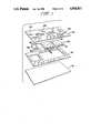
- FIG. 1is an exploded, isometric view providing a partially schematic representation of the packaging configuration and method of the present invention
- FIG. 2is a cross-sectional side elevation view illustrating an interchip connection in accordance with the present invention
- FIG. 3Ais a view similar to FIG. 2 which more particularly illustrates the utilization of multiple overlay films for more complicated and nonplanar interconnection arrangements;
- FIG. 3Bis a figure similar to FIG. 3A which more particularly illustrates the utilization of a laminated film layer together with a second applied polymer layer.
- FIG. 1illustrates an exploded view of one embodiment of the present invention.
- the packaging layerincludes optional packing insert 12 having apertures into which chips 15a, 15b and 15c are placed.
- the packaging layerincludes optional packing insert 12 having apertures into which chips 15a, 15b and 15c are placed.
- the number and arrangement of integrated circuit chips shown in FIG. 1is solely for the purpose of illustration.
- the placement of interconnect pads 16 on the chips and the placement of interconnect metallization patterns 25 on layer 20is likewise merely exemplary. There may be more chips or fewer chips configured in numerous arrangements and interconnected in numerous different fashions, as determined by conductive patterns on overlay layer 20 and packaging insert 12 and most importantly by the desired function of the chip system.
- packaging insert 12is preferred, but is optional.
- Substrate 10may comprise a number of different materials.
- a substrate of aluminais possible.
- Substrate 10may also include a metal such as copper, for the purpose of maximum heat removal, or maximum electrical conductivity.
- Other examples of substrate materialsinclude ceramic multilayer circuits or even silicon which can provide good thermal conductivity and virtually an identical thermal coefficient of expansion with respect to silicon especially when integrated circuit chips 15a, 15b and 15c are silicon based.
- the chipsdo not necessarily have to comprise silicon based semiconductor devices, but may also include gallium arsenide or other type devices.
- the same circuit technologiesdo not have to be employed on all chips. Chip technology types may be mixed and matched as appropriate.
- Substrate layer 10may also comprise glass, plastic materials and, if necessary, composites. The most important property of substrate layer 10 is that its coefficient of thermal expansion be approximately equal to the coefficient of thermal expansion of other materials employed in the assembly.
- the second layer shown in FIG. 1is the optional packaging layer which includes packing insert 12.
- Packaging insert 12may be employed to provide interconnections between the chips and the pins of the package as well as to provide connection for power and ground, if necessary.
- This layercan be fabricated by a number of different means. In basic systems where no additional interconnect capability is required, this layer simply comprises a punched lamination with no included interconnect metallization.
- packing insert 12can be fabricated using thick film methods in which a layer of dielectric is printed and fired, followed by subsequent layers of conductor or dielectric.
- a third alternativeis to fabricate this layer as part of a multilayer ceramic circuit in which the bottom of the ceramics bond to the substrate and the intermediate layers form packing insert 12.
- Chips 15a-15care mounted in place by any one of a number of methods for die attachment. Such methods include eutectic die bonding, epoxy die bonding and thermoplastic die bonding. In eutectic die bonding, a gold germanium solder preform is placed under each chip and the substrate is subsequently heated to the eutectic melting point of the gold germanium preform. A silicon-gold solder eutectic is formed.
- a second alternativeinvolves the use of a thermosetting epoxy which can either be loaded with silver or with gold to achieve electrical conductivity, or filled with alumina or beryllia to achieve thermal conductivity. Epoxy is applied by screen printing methods or by dispensing from a needle tip.
- a third alternativeinvolves applying a thermoplastic such as ULTEM® resin (as sold by the General Electric Company) or silicon polyimide to the substrate using a solvent such as NMP (N-methyl pyrolidone).
- ULTEM® resinas sold by the General Electric Company
- NMPN-methyl pyrolidone
- the chipsare subsequently placed in the thermoplastic and again, heat is applied with an oven or hot plate until the thermoplastic melts and/or residual solvent is driven off. Upon cooling, the chips are thus bonded to the substrate. At this point a polymer overlayer is laminated over the tops of the chips.
- laminationis achieved by first spraying the chips and the packaging insert layer with a thin layer of ULTEM® 1000 resin and a solvent of methylene chloride and acetophenone. This layer is then dried at a temperature of from approximately 200° C. to approximately 300° C. for a period of approximately 5 minutes and is used as a thermoplastic adhesive for bonding a 1 mil thick KAPTON® film layer to the chip.
- KAPTON®is a registered trademark of the Dupont de Nemours Company, Inc.
- Laminationmay be achieved using conventional laminators and using a silicone rubber press pad to amortize the height differential.
- laminationscan be achieved using the vacuum-pressure laminator as disclosed in the aforementioned application Ser. No. 240,367.
- the laminating temperature usedis the temperature at which the thermoplastic adhesive melts. In the case of ULTEM® resin, the temperature is between approximately 250° C. and 350° C.
- Via holesare now formed in the structure resulting from the above process steps. Via holes are formed above those interconnect pads on the circuit chips where interconnection to power, ground, signal or packaging pins is desired. Via holes are formed by depositing a thin layer of metallization, such as for example, a 1,000 angstrom thick layer of titanium or chrome on the polymer surface. Via opening positions are then patterned in the layer using conventional photolithography methods. That is, a layer of photoresist is deposited, dried, and exposed through a mask and subsequently developed. For example, when titanium is used, it is etched with a solution of fluoroboric acid, and the titanium is then used as an etch mask in an oxygen-plasma reactive ion etching device. In this way, holes are etched in the polymer, but the oxygen plasma does not attack the metal pads of the integrated circuit chip or of packing insert 12.
- a thin layer of metallizationsuch as for example, a 1,000 angstrom thick layer of titanium or chrome on the polymer surface.
- Via opening positions
- Metallizationis now preferably applied by first using a glow discharge to clean the surface of the chip pads and the surface of the packing insert layer. After cleaning, a buffer layer of metallization, such as titanium or chrome is applied to cover the entire surface of the overlay layer and to fill the via holes and to contact the top of the interconnection pads of the chip and the packing insert.
- the titanium or chrome metallizationwhich is optional, is deposited to a thickness of approximately 1,000 angstroms. These metallizations are used for four specific reasons. First, they form a buffer layer to prevent subsequently deposited copper metallization from migrating through the pads of the chip and causing spiking into the chip substrate.
- titanium and chromeare relatively reactive metals and form stable chemical bonds between the polymer of overlay layer 20 and subsequently applied metallization.
- titanium and chromereact with aluminum oxide to give good ohmic contact to the chip pads.
- titanium and chromeare metals which are not attacked by etching solutions which attack copper which is a preferred metal for subsequent deposition. This allows the copper to be completely removed during an interconnection removal process which is described in more detail below.
- a deposit of copperis sputtered directly on the titanium or chrome deposit. Copper is used to provide a high degree of conductivity. Copper is deposited to a thickness of between approximately 2 and approximately 5 microns. After copper deposition, the substrate is removed from the sputtering chamber and a layer of photoresist is deposited on the surface of the copper either by spraying or spinning methods. The resist is then exposed using a contact mask according to the desired metallization pattern. After the resist has been developed, the structure is etched. A solution comprising 600 grams nitric acid, 600 grams sulfuric acid and 600 grams of H 3 PO 4 in 1.5 liters of water is usable for this purpose.
- the titaniumfor example, is etched using a solution of fluoroboric acid.
- the titanium layeris etched using reactive ion etching in a CF 4 plasma.
- Using plasma to remove the barrier metalsis attractive because it prevents the polymer from being directly exposed at any time in the process to wet processing steps which might cause the polymer to absorb small amounts of the wet processing material which could later attack the chip surface.
- An alternative to the contact mask method of exposing the photoresistis to use a laser which is scanned under control of a computer according to the method disclosed in application Ser. No. 947,461, filed Dec. 29, 1986 and assigned to the instant assignee.
- the metallizationis patterned to form very fine lines and spaces, typically under 1 mil in line width and 1 mil in line spacing. Tests performed using an adaptive lithography system, have demonstrated 6 micron lines and spaces the present invention. In addition, it can be seem from FIG. 1, that chips can now essentially be placed edge to edge. Chips are easily interconnected because the metallization pitch (1-mil lines and space) is much finer than the pad spacing (typically 10 mil) associated with the chips themselves.
- the resulting structureis one in which the interconnect length is as short as possible, and in which the width of the conductors is from about 6 to about 25 microns.
- the dielectricis typically 1 mil thick with a dielectric constant midway between the relative dielectric constants of ULTEM® resin and KAPTON® films, or approximately 3.2. This results in a very low capacitance loading system. It should also be noted that the interconnect length and capacitive loading of the present system is substantially lower than is achieved in any other approach. It should also be noted that with chips placed edge to edge, a minimum ratio between the overall package size and the area of silicon involved is achieved. Also, note that there is only one interconnect run and two interconnects required to connect from one chip to another and, additionally, the interconnect run is an integral part of the interconnect. No known art provides for fewer interconnects or for an interconnect run to be an integral part of the interconnect.
- the interconnect and the interconnect runis preferably formed by vacuum sputter methods such that the surface receiving metallization pattern is cleaned by sputtering, followed by immediate metallization.
- This methodresults in highly reliable interconnections with very low contamination levels. This method is superior to those methods utilizing soldering which can involve contamination from flux and from oxidation due to heating of the system in an air environment.
- FIG. 2shows a cross-section of a resulting high density interconnection structure in accordance with the present invention.
- a bridgecomprising flexible polymer material 20 and a layer of thin metallization between two interconnected chips.
- Polymer layer 20 and metallization patterns 25are also seen in a broader perspective view in FIG. 1.
- the layer of metallizationincludes copper metallization 25, as described above, and also preferably includes optional titanium barrier layer 24.
- adhesive 19is preferably employed to affix polymer layer 20 to the substrate/chip structure. It is, however, noted that adhesive layer 19 is generally optional and is not necessarily included in every fabrication methods.
- the relatively flexible polymeris stretched or compressed as necessary to to accommodate the differential movement.
- Metallization 25preferably including copper also accommodates differential expansion with essentially no stress applied to the interconnect area. Thermally induced stress is a significant problem in other known structures such as the solder bump structure and in chip carrier structures where the package containing the chip is soldered, without leads, to a non-thermally matched circuit board.
- the interconnect area required by the process of the present inventionis only limited by the size of the via hole and the ability to pattern the metallization layer.
- via holes of 6 micronshave been achieved using maskless via hole processes as described in aforementioned U.S. Pat. No. 4,714,516.
- Metallization patterning in the 6 to 25 micron regionhas also been achieved. Therefore, a 6 to 25 micron diameter region is all the area required for an interconnection. This has profound implications on the area required for interconnection pads positioned on a chip for the purpose of making connections. It can also be seen from FIG. 1 that it is not necessary that the chip pads be confined to the periphery of the chip.
- an additional dielectric metallization layeris applied by any of a number of means.
- a second dielectric layeris applied.
- the dielectric layercan be applied by spraying an adhesive, as described above, which comprises ULTEM® resin in a solvent of methylene chloride and acectophenone.
- an adhesiveas described above, which comprises ULTEM® resin in a solvent of methylene chloride and acectophenone.
- a second layercomprising KAPTON® film is laminated over the existing structure.
- Via holesare then fabricated either by metal mask and etching or by maskless via hole information using a laser as described in U.S. Pat. No. 4,714,516.
- Metallizationis applied by sputtering, as above.
- FIG. 3Ashows a cross-section of the resulting structure.
- attentionis directed to second adhesive layer 29, second polymer layer 30 and second metallization layer which includes second titanium barrier layer 34 together with interconnect conductor 35, preferably comprising copper, as above.
- FIG. 3Bshows a multilayer system, in cross-sectional view, in which the second dielectric layer comprises an ULTEM® resin or other polymer dielectric which is sprayed over the first layer.
- the same mixture which is used for the adhesive layer as described aboveis used as the dielectric layer.
- a first layeris sprayed and dried at a temperature of between approximately 250° C. and approximately 350° C. for a period of about 5 minutes.
- a second layeris sprayed and dried as before.
- a third layeris sprayed and dried. This results in a layer approximately 12 microns thick. Via holes and metallization are fabricated as described above.
- a third alternativeis to use paraxylene as the dielectric.
- the deposition of this materialinvolves heating the substrate in a vacuum of approximately 1 torr and admitting the paraxylene monomer in a controlled manner such that a polymer is formed on all exposed surfaces of the substrate.
- Such chemical vapor depositionis characterized by a very even coating which is free of pinholes. Via holes and metallization are then formed as described above.
- polymer layer 20is typically approximately 12 to 25 microns thick.
- Each of the adhesive layers 19 and 29are typically approximately 3 microns thick.
- the second polymer layeris typically 12 microns thick particularly in the event that it is an applied, as opposed to a laminated film layer.
- Titanium barriers 24 and 34are each typically approximately 0.1 to 0.2 microns thick.
- each of the copper metallization layers 25 and 35are typically approximately 3 to 6 microns thick.
- the coppermay be deposited by sputtering or vacuum deposition. However, neither of these methods is presently preferred over the other.
- overlay layer 20may be removed.
- removal of layersmay be effected in a batch process which comprises alternately etching or dissolving metallization layer, followed by etching or dissolving a polymer layer. This process is continued until the only remaining layers are the polymer film and metallization layers which were first applied. At this point, copper metallization is removed by dissolving it in a bath of nitric acid, sulfuric acid and H 3 PO 4 as described above. Since titanium is unattacked by this etchant, it remains.
- the titaniumis removed by dipping the structure in a solution of fluoroboric acid or alternatively, in a presently preferred embodiment, by reactive ion etching in an atmosphere of gaseous CF 4 . Since the titanium layer is relatively thin (approximately 1,000 angstroms), it is quickly removed by the plasma. Plasma devices operating at an RF input of 150 watts for period of approximately 5 minutes are used to achieve the desired result. Any exposed pads on the chip and on the packing layer are beneficially cleaned by the plasma. At this point, the plasma gas can be changed to an oxygen plasma enhanced by CF 4 .
- the substrateis soaked in methylene chloride for 2 hours which lifts off KAPTON® film material.
- Individual chip componentsare now removed by heating the substrate to the softening point of the particular die attachment method. Typically, this is the melting point of the solder if eutectic die attachment was used, or the deflection point (or above) of the epoxy if an epoxy die attachment is used, or the melting point of the thermoplastic, if a thermoplastic die attachment method is used. A new chip is then used to replace any bad chips and the process can be repeated.
- the ability to remove the overlay layeris very significant. It permits the fabrication of multichip integrated circuit packages in which the chips are first arranged in a test configuration. This is highly significant for purposes of testability. As chip systems become more and more complicated, both in their own circuitry and in their interconnections and interactions, testing of the resulting chips and systems becomes more and more difficult. The level of difficulty for chip testing can in fact be seen to grow at a rate greater than exponential growth because of the combinatorically greater complexity. However, the removability of the overlay layer together with the ability to apply a new layer and to connect the chips in a different pattern and to remove defective chips, effectively achieves wafer scale integration, without sacrificing in any way testability constraints.
- the polymer film(or multilevel films) provide a removable insulative structure in which vias are provided and on which metallization patterns are disposed for the purpose of intrachip connection and/or for the purpose of connecting select chip pads to exterior pins or pads disposed on the substrate to which the chip is affixed.
- the packaging configuration and method of the present inventionsignificantly advances the semiconductor packaging arts.
- the method of the present inventioncan be used to interconnect multiple packages in accordance with the present invention, that is, a second or third overlay layer may be employed to connect sets of multichip packages, each of which is fabricated in accordance with the present invention.
- the configuration and methods described hereinare economic and readily achieved without fabrication complexity.
- the processing methods described hereinprovide significant advantages with respect to the physical and electrical characteristics of the resulting circuit packages.
- the system of the present inventionfully satisfies all of the aforementioned objects.
Landscapes
- Engineering & Computer Science (AREA)
- Computer Hardware Design (AREA)
- Microelectronics & Electronic Packaging (AREA)
- Power Engineering (AREA)
- Physics & Mathematics (AREA)
- Condensed Matter Physics & Semiconductors (AREA)
- General Physics & Mathematics (AREA)
- Wire Bonding (AREA)
Abstract
Description
Claims (5)
Priority Applications (1)
| Application Number | Priority Date | Filing Date | Title |
|---|---|---|---|
| US07/391,398US4918811A (en) | 1986-09-26 | 1989-08-08 | Multichip integrated circuit packaging method |
Applications Claiming Priority (3)
| Application Number | Priority Date | Filing Date | Title |
|---|---|---|---|
| US06/912,456US4783695A (en) | 1986-09-26 | 1986-09-26 | Multichip integrated circuit packaging configuration and method |
| US21518788A | 1988-07-05 | 1988-07-05 | |
| US07/391,398US4918811A (en) | 1986-09-26 | 1989-08-08 | Multichip integrated circuit packaging method |
Related Parent Applications (2)
| Application Number | Title | Priority Date | Filing Date |
|---|---|---|---|
| US06/912,456DivisionUS4783695A (en) | 1986-09-26 | 1986-09-26 | Multichip integrated circuit packaging configuration and method |
| US21518788AContinuation | 1986-09-26 | 1988-07-05 |
Publications (1)
| Publication Number | Publication Date |
|---|---|
| US4918811Atrue US4918811A (en) | 1990-04-24 |
Family
ID=27396090
Family Applications (1)
| Application Number | Title | Priority Date | Filing Date |
|---|---|---|---|
| US07/391,398Expired - LifetimeUS4918811A (en) | 1986-09-26 | 1989-08-08 | Multichip integrated circuit packaging method |
Country Status (1)
| Country | Link |
|---|---|
| US (1) | US4918811A (en) |
Cited By (123)
| Publication number | Priority date | Publication date | Assignee | Title |
|---|---|---|---|---|
| US5091769A (en)* | 1991-03-27 | 1992-02-25 | Eichelberger Charles W | Configuration for testing and burn-in of integrated circuit chips |
| US5111278A (en)* | 1991-03-27 | 1992-05-05 | Eichelberger Charles W | Three-dimensional multichip module systems |
| US5144747A (en)* | 1991-03-27 | 1992-09-08 | Integrated System Assemblies Corporation | Apparatus and method for positioning an integrated circuit chip within a multichip module |
| EP0515094A1 (en)* | 1991-05-23 | 1992-11-25 | AT&T Corp. | Molded circuit package |
| US5182420A (en)* | 1989-04-25 | 1993-01-26 | Cray Research, Inc. | Method of fabricating metallized chip carriers from wafer-shaped substrates |
| US5183972A (en)* | 1991-02-04 | 1993-02-02 | Microelectronics And Computer Technology Corporation | Copper/epoxy structures |
| US5196377A (en)* | 1990-12-20 | 1993-03-23 | Cray Research, Inc. | Method of fabricating silicon-based carriers |
| US5216806A (en)* | 1992-09-01 | 1993-06-08 | Atmel Corporation | Method of forming a chip package and package interconnects |
| US5249100A (en)* | 1989-05-19 | 1993-09-28 | Hitachi, Ltd. | Electronic circuit device provided with a ceramic substrate having lead pins bonded thereto by solder |
| US5250843A (en)* | 1991-03-27 | 1993-10-05 | Integrated System Assemblies Corp. | Multichip integrated circuit modules |
| US5279706A (en)* | 1992-10-13 | 1994-01-18 | General Electric Company | Method and apparatus for fabricating a metal interconnection pattern for an integrated circuit module |
| US5291066A (en)* | 1991-11-14 | 1994-03-01 | General Electric Company | Moisture-proof electrical circuit high density interconnect module and method for making same |
| US5346861A (en)* | 1990-09-24 | 1994-09-13 | Tessera, Inc. | Semiconductor chip assemblies and methods of making same |
| US5348607A (en)* | 1989-02-21 | 1994-09-20 | General Electric Company | High density interconnect thermoplastic die attach material and solvent die attach processing |
| US5365403A (en)* | 1992-07-17 | 1994-11-15 | Vlt Corporation | Packaging electrical components |
| US5373627A (en)* | 1993-11-23 | 1994-12-20 | Grebe; Kurt R. | Method of forming multi-chip module with high density interconnections |
| US5386623A (en)* | 1990-11-15 | 1995-02-07 | Hitachi, Ltd. | Process for manufacturing a multi-chip module |
| US5399505A (en)* | 1993-07-23 | 1995-03-21 | Motorola, Inc. | Method and apparatus for performing wafer level testing of integrated circuit dice |
| US5401688A (en)* | 1991-02-18 | 1995-03-28 | Kabushiki Kaisha Toshiba | Semiconductor device of multichip module-type |
| US5407864A (en)* | 1992-07-24 | 1995-04-18 | Samsung Electronics Co., Ltd. | Process for mounting a semiconductor chip and depositing contacts into through holes of a circuit board and of an insulating interposer and onto the chip |
| US5455459A (en)* | 1992-03-27 | 1995-10-03 | Martin Marietta Corporation | Reconstructable interconnect structure for electronic circuits |
| US5468992A (en)* | 1991-02-28 | 1995-11-21 | Hitachi, Ltd. | Electronic circuit package including plural bare chips mounted on a single wiring substrate |
| US5489059A (en)* | 1990-08-15 | 1996-02-06 | Lsi Logic Corporation | Semiconductor device having an universal die size inner lead layout |
| US5524339A (en)* | 1994-09-19 | 1996-06-11 | Martin Marietta Corporation | Method for protecting gallium arsenide mmic air bridge structures |
| US5567657A (en)* | 1995-12-04 | 1996-10-22 | General Electric Company | Fabrication and structures of two-sided molded circuit modules with flexible interconnect layers |
| US5594273A (en)* | 1993-07-23 | 1997-01-14 | Motorola Inc. | Apparatus for performing wafer-level testing of integrated circuits where test pads lie within integrated circuit die but overly no active circuitry for improved yield |
| US5644103A (en)* | 1994-11-10 | 1997-07-01 | Vlt Corporation | Packaging electrical components having a scallop formed in an edge of a circuit board |
| US5654588A (en)* | 1993-07-23 | 1997-08-05 | Motorola Inc. | Apparatus for performing wafer-level testing of integrated circuits where the wafer uses a segmented conductive top-layer bus structure |
| US5663106A (en)* | 1994-05-19 | 1997-09-02 | Tessera, Inc. | Method of encapsulating die and chip carrier |
| US5679977A (en)* | 1990-09-24 | 1997-10-21 | Tessera, Inc. | Semiconductor chip assemblies, methods of making same and components for same |
| US5701666A (en)* | 1994-08-31 | 1997-12-30 | Motorola, Inc. | Method for manufacturing a stimulus wafer for use in a wafer-to-wafer testing system to test integrated circuits located on a product wafer |
| US5727727A (en)* | 1995-02-02 | 1998-03-17 | Vlt Corporation | Flowing solder in a gap |
| US5728600A (en)* | 1994-11-15 | 1998-03-17 | Vlt Corporation | Circuit encapsulation process |
| US5776796A (en)* | 1994-05-19 | 1998-07-07 | Tessera, Inc. | Method of encapsulating a semiconductor package |
| US5808358A (en)* | 1994-11-10 | 1998-09-15 | Vlt Corporation | Packaging electrical circuits |
| US5820014A (en) | 1993-11-16 | 1998-10-13 | Form Factor, Inc. | Solder preforms |
| US5834334A (en)* | 1992-04-08 | 1998-11-10 | Elm Technology Corporation | Method of forming a multi-chip module from a membrane circuit |
| US5876859A (en)* | 1994-11-10 | 1999-03-02 | Vlt Corporation | Direct metal bonding |
| US5925260A (en)* | 1997-01-02 | 1999-07-20 | Micron Technology, Inc. | Removal of polyimide from dies and wafers |
| US5929517A (en)* | 1994-12-29 | 1999-07-27 | Tessera, Inc. | Compliant integrated circuit package and method of fabricating the same |
| US5945130A (en)* | 1994-11-15 | 1999-08-31 | Vlt Corporation | Apparatus for circuit encapsulation |
| US5994152A (en) | 1996-02-21 | 1999-11-30 | Formfactor, Inc. | Fabricating interconnects and tips using sacrificial substrates |
| US6027958A (en)* | 1996-07-11 | 2000-02-22 | Kopin Corporation | Transferred flexible integrated circuit |
| US6031726A (en)* | 1995-11-06 | 2000-02-29 | Vlt Corporation | Low profile mounting of power converters with the converter body in an aperture |
| US6133627A (en)* | 1990-09-24 | 2000-10-17 | Tessera, Inc. | Semiconductor chip package with center contacts |
| US6214640B1 (en) | 1999-02-10 | 2001-04-10 | Tessera, Inc. | Method of manufacturing a plurality of semiconductor packages |
| US6232152B1 (en) | 1994-05-19 | 2001-05-15 | Tessera, Inc. | Method of manufacturing a plurality of semiconductor packages and the resulting semiconductor package structures |
| US6234842B1 (en) | 1998-11-20 | 2001-05-22 | Vlt Corporation | Power converter connector assembly |
| US6240634B1 (en)* | 1997-09-12 | 2001-06-05 | Fujitsu Limited | Method of producing a multichip package module in which rough-pitch and fine-pitch chips are mounted on a board |
| US6251219B1 (en) | 1998-09-17 | 2001-06-26 | Intermedics Inc. | Method and apparatus for use in assembling electronic devices |
| US6259140B1 (en)* | 1999-02-02 | 2001-07-10 | Macronix International Co., Ltd. | Silicide blocking process to form non-silicided regions on MOS devices |
| US6274823B1 (en) | 1993-11-16 | 2001-08-14 | Formfactor, Inc. | Interconnection substrates with resilient contact structures on both sides |
| US20010030370A1 (en)* | 1990-09-24 | 2001-10-18 | Khandros Igor Y. | Microelectronic assembly having encapsulated wire bonding leads |
| US6316737B1 (en) | 1999-09-09 | 2001-11-13 | Vlt Corporation | Making a connection between a component and a circuit board |
| US6359335B1 (en) | 1994-05-19 | 2002-03-19 | Tessera, Inc. | Method of manufacturing a plurality of semiconductor packages and the resulting semiconductor package structures |
| US6434005B1 (en) | 2000-10-27 | 2002-08-13 | Vlt Corporation | Power converter packaging |
| US6468638B2 (en)* | 1999-03-16 | 2002-10-22 | Alien Technology Corporation | Web process interconnect in electronic assemblies |
| US20020155728A1 (en)* | 1990-09-24 | 2002-10-24 | Tessera, Inc. | Semiconductor chip assemblies, methods of making same and components for same |
| US6505665B1 (en) | 1998-09-17 | 2003-01-14 | Intermedics, Inc. | Method and apparatus for use in assembling electronic devices |
| US6510606B2 (en)* | 1998-06-15 | 2003-01-28 | Lockheed Martin Corporation | Multichip module |
| US6519843B2 (en)* | 1998-11-18 | 2003-02-18 | International Business Machines Corporation | Method of forming a chip carrier by joining a laminate layer and stiffener |
| US20030059976A1 (en)* | 2001-09-24 | 2003-03-27 | Nathan Richard J. | Integrated package and methods for making same |
| US20030057544A1 (en)* | 2001-09-13 | 2003-03-27 | Nathan Richard J. | Integrated assembly protocol |
| US20030067020A1 (en)* | 2001-10-10 | 2003-04-10 | Masanori Itoh | Semiconductor device |
| US20030107118A1 (en)* | 2001-10-09 | 2003-06-12 | Tessera, Inc. | Stacked packages |
| US20030122244A1 (en)* | 2001-12-31 | 2003-07-03 | Mou-Shiung Lin | Integrated chip package structure using metal substrate and method of manufacturing the same |
| US20030122246A1 (en)* | 2001-12-31 | 2003-07-03 | Mou-Shiung Lin | Integrated chip package structure using silicon substrate and method of manufacturing the same |
| US20030153119A1 (en)* | 2002-02-14 | 2003-08-14 | Nathan Richard J. | Integrated circuit package and method for fabrication |
| US20030227079A1 (en)* | 2002-06-11 | 2003-12-11 | Micron Technology, Inc. | Super high density module with integrated wafer level packages |
| US20040031972A1 (en)* | 2001-10-09 | 2004-02-19 | Tessera, Inc. | Stacked packages |
| US6715203B2 (en)* | 2000-02-18 | 2004-04-06 | Eupec Europaeische Gesellschaft Fuer Leistungshalbleiter Mbh & Co. Kg | Substrate for power semiconductor modules with through-plating of solder and method for its production |
| US20040100778A1 (en)* | 2002-11-25 | 2004-05-27 | Patrizio Vinciarelli | Power converter package and thermal management |
| US20040105244A1 (en)* | 2002-08-06 | 2004-06-03 | Ilyas Mohammed | Lead assemblies with offset portions and microelectronic assemblies with leads having offset portions |
| US20040160714A1 (en)* | 2001-04-24 | 2004-08-19 | Vlt Corporation, A Texas Corporation | Components having actively controlled circuit elements |
| US20040183182A1 (en)* | 2002-01-23 | 2004-09-23 | Susan Swindlehurst | Apparatus incorporating small-feature-size and large-feature-size components and method for making same |
| US20040188531A1 (en)* | 2003-03-24 | 2004-09-30 | Gengel Glenn W. | RFID tags and processes for producing RFID tags |
| US20040229400A1 (en)* | 2002-08-27 | 2004-11-18 | Chua Swee Kwang | Multichip wafer level system packages and methods of forming same |
| US6903458B1 (en) | 2002-06-20 | 2005-06-07 | Richard J. Nathan | Embedded carrier for an integrated circuit chip |
| US20050176180A1 (en)* | 2004-02-09 | 2005-08-11 | Fay Owen R. | Die encapsulation using a porous carrier |
| US20050173796A1 (en)* | 2001-10-09 | 2005-08-11 | Tessera, Inc. | Microelectronic assembly having array including passive elements and interconnects |
| USD510906S1 (en) | 2000-10-27 | 2005-10-25 | Vlt, Inc. | Power converter |
| US20050270757A1 (en)* | 2001-05-31 | 2005-12-08 | Credelle Thomas L | Electronic devices with small functional elements supported on a carrier |
| US20060049530A1 (en)* | 2004-09-09 | 2006-03-09 | Phoenix Precision Technology Corporation | Method of embedding semiconductor chip in support plate and embedded structure thereof |
| USD520947S1 (en) | 2001-11-01 | 2006-05-16 | Vlt, Inc. | Power converter body |
| US20060109123A1 (en)* | 2004-11-22 | 2006-05-25 | Curt Carrender | Radio frequency identification (RFID) tag for an item having a conductive layer included or attached |
| US20060109130A1 (en)* | 2004-11-22 | 2006-05-25 | Hattick John B | Radio frequency identification (RFID) tag for an item having a conductive layer included or attached |
| US20060128066A1 (en)* | 2004-12-10 | 2006-06-15 | Lytle William H | Flexible carrier and release method for high volume electronic package fabrication |
| US20070006456A1 (en)* | 2005-07-07 | 2007-01-11 | Samsung Electro-Mechanics Co., Ltd. | Method for manufacturing circuit board with built-in electronic components |
| US20070210461A1 (en)* | 2006-03-10 | 2007-09-13 | Fay Owen R | Semiconductor device packaging |
| US20080093727A1 (en)* | 2004-11-29 | 2008-04-24 | Karl Weidner | Metallised Film For Sheet Contacting |
| US20080094805A1 (en)* | 2004-11-26 | 2008-04-24 | Imbera Electroics Oy | Electronics Module and Method for Manufacturing the Same |
| US20080123318A1 (en)* | 2006-11-08 | 2008-05-29 | Atmel Corporation | Multi-component electronic package with planarized embedded-components substrate |
| US7443229B1 (en) | 2001-04-24 | 2008-10-28 | Picor Corporation | Active filtering |
| US20080318413A1 (en)* | 2007-06-21 | 2008-12-25 | General Electric Company | Method for making an interconnect structure and interconnect component recovery process |
| US20080318027A1 (en)* | 2007-06-21 | 2008-12-25 | General Electric Company | Demountable interconnect structure |
| US20080313894A1 (en)* | 2007-06-21 | 2008-12-25 | General Electric Company | Method for making an interconnect structure and low-temperature interconnect component recovery process |
| US20080318054A1 (en)* | 2007-06-21 | 2008-12-25 | General Electric Company | Low-temperature recoverable electronic component |
| US20080318055A1 (en)* | 2007-06-21 | 2008-12-25 | General Electric Company | Recoverable electronic component |
| US20080314867A1 (en)* | 2007-06-21 | 2008-12-25 | General Electric Company | Method of making demountable interconnect structure |
| US20090039530A1 (en)* | 2007-08-07 | 2009-02-12 | Fryklund David J | Near chip scale package integration process |
| US20090061564A1 (en)* | 2007-08-29 | 2009-03-05 | Freescale Semiconductor, Inc. | Method of packaging an integrated circuit die |
| US20090221114A1 (en)* | 2008-02-29 | 2009-09-03 | Freescale Semiconductor, Inc. | Packaging an integrated circuit die using compression molding |
| US7601039B2 (en) | 1993-11-16 | 2009-10-13 | Formfactor, Inc. | Microelectronic contact structure and method of making same |
| US20090320139A1 (en)* | 2004-11-22 | 2009-12-24 | Curt Carrender | Transponder incorporated into an electronic device |
| US20100112756A1 (en)* | 2008-11-06 | 2010-05-06 | Amrine Craig S | Integrated circuit package formation |
| US20100252919A1 (en)* | 2009-04-07 | 2010-10-07 | Freescale Semiconductor, Inc. | Electronic device and method of packaging an electronic device |
| US7838892B2 (en) | 2004-04-29 | 2010-11-23 | Osram Opto Semiconductors Gmbh | Optoelectronic semiconductor chip and method for forming a contact structure for making electrical contact with an optoelectronic semiconductor chip |
| US20110119910A1 (en)* | 2009-11-23 | 2011-05-26 | Freescale Semiconductor, Inc. | Method and system for releasing a microelectronic assembly from a carrier substrate |
| US20110205720A1 (en)* | 2001-12-31 | 2011-08-25 | Megica Corporation | Integrated chip package structure using organic substrate and method of manufacturing the same |
| US8033838B2 (en) | 1996-02-21 | 2011-10-11 | Formfactor, Inc. | Microelectronic contact structure |
| USRE43404E1 (en) | 1996-03-07 | 2012-05-22 | Tessera, Inc. | Methods for providing void-free layer for semiconductor assemblies |
| DE102011083627A1 (en)* | 2011-09-28 | 2013-03-28 | Continental Automotive Gmbh | Method for connecting electronic part e.g. transistor, involves applying electrical conductive layer for electrically connecting electrical contact surface of electronic part with electrical strip conductor, and applying covering layer |
| US8492870B2 (en) | 2002-01-19 | 2013-07-23 | Megica Corporation | Semiconductor package with interconnect layers |
| US8535976B2 (en) | 2001-12-31 | 2013-09-17 | Megica Corporation | Method for fabricating chip package with die and substrate |
| US8617935B2 (en) | 2011-08-30 | 2013-12-31 | Freescale Semiconductor, Inc. | Back side alignment structure and manufacturing method for three-dimensional semiconductor device packages |
| US20140110859A1 (en)* | 2012-10-09 | 2014-04-24 | Mc10, Inc. | Embedding thin chips in polymer |
| US20140118966A1 (en)* | 2012-10-29 | 2014-05-01 | Lsi Corporation | Low Inductance Flex Bond with Low Thermal Resistance |
| US8847409B1 (en) | 2013-06-03 | 2014-09-30 | Teledyne Scientific & Imaging, Llc | Compliant micro-socket hybridization method |
| US9029259B2 (en) | 2012-02-17 | 2015-05-12 | Teledyne Scientific & Imaging, Llc | Self-aligning hybridization method |
| US9236366B2 (en) | 2012-12-20 | 2016-01-12 | Intel Corporation | High density organic bridge device and method |
| EP2184777B1 (en)* | 2008-11-07 | 2017-05-03 | General Electric Company | Interconnect structure |
| US20190164925A1 (en)* | 2017-09-28 | 2019-05-30 | Taiwan Semiconductor Manufacturing Co., Ltd. | Semiconductor structure |
| US11124737B2 (en) | 2012-04-25 | 2021-09-21 | Commonwealth Scientific Andn Industrial Research Organisation | High oleic acid oils |
Citations (3)
| Publication number | Priority date | Publication date | Assignee | Title |
|---|---|---|---|---|
| US3501832A (en)* | 1966-02-26 | 1970-03-24 | Sony Corp | Method of making electrical wiring and wiring connections for electrical components |
| US3903590A (en)* | 1973-03-10 | 1975-09-09 | Tokyo Shibaura Electric Co | Multiple chip integrated circuits and method of manufacturing the same |
| US4709468A (en)* | 1986-01-31 | 1987-12-01 | Texas Instruments Incorporated | Method for producing an integrated circuit product having a polyimide film interconnection structure |
- 1989
- 1989-08-08USUS07/391,398patent/US4918811A/ennot_activeExpired - Lifetime
Patent Citations (3)
| Publication number | Priority date | Publication date | Assignee | Title |
|---|---|---|---|---|
| US3501832A (en)* | 1966-02-26 | 1970-03-24 | Sony Corp | Method of making electrical wiring and wiring connections for electrical components |
| US3903590A (en)* | 1973-03-10 | 1975-09-09 | Tokyo Shibaura Electric Co | Multiple chip integrated circuits and method of manufacturing the same |
| US4709468A (en)* | 1986-01-31 | 1987-12-01 | Texas Instruments Incorporated | Method for producing an integrated circuit product having a polyimide film interconnection structure |
Cited By (245)
| Publication number | Priority date | Publication date | Assignee | Title |
|---|---|---|---|---|
| US5348607A (en)* | 1989-02-21 | 1994-09-20 | General Electric Company | High density interconnect thermoplastic die attach material and solvent die attach processing |
| US5182420A (en)* | 1989-04-25 | 1993-01-26 | Cray Research, Inc. | Method of fabricating metallized chip carriers from wafer-shaped substrates |
| US5249100A (en)* | 1989-05-19 | 1993-09-28 | Hitachi, Ltd. | Electronic circuit device provided with a ceramic substrate having lead pins bonded thereto by solder |
| US5489059A (en)* | 1990-08-15 | 1996-02-06 | Lsi Logic Corporation | Semiconductor device having an universal die size inner lead layout |
| US5682061A (en)* | 1990-09-24 | 1997-10-28 | Tessera, Inc. | Component for connecting a semiconductor chip to a substrate |
| US5679977A (en)* | 1990-09-24 | 1997-10-21 | Tessera, Inc. | Semiconductor chip assemblies, methods of making same and components for same |
| US7198969B1 (en) | 1990-09-24 | 2007-04-03 | Tessera, Inc. | Semiconductor chip assemblies, methods of making same and components for same |
| US7271481B2 (en) | 1990-09-24 | 2007-09-18 | Tessera, Inc. | Microelectronic component and assembly having leads with offset portions |
| US7291910B2 (en) | 1990-09-24 | 2007-11-06 | Tessera, Inc. | Semiconductor chip assemblies, methods of making same and components for same |
| US20020155728A1 (en)* | 1990-09-24 | 2002-10-24 | Tessera, Inc. | Semiconductor chip assemblies, methods of making same and components for same |
| US7098078B2 (en) | 1990-09-24 | 2006-08-29 | Tessera, Inc. | Microelectronic component and assembly having leads with offset portions |
| US20050087855A1 (en)* | 1990-09-24 | 2005-04-28 | Tessera, Inc. | Microelectronic component and assembly having leads with offset portions |
| US5346861A (en)* | 1990-09-24 | 1994-09-13 | Tessera, Inc. | Semiconductor chip assemblies and methods of making same |
| US5950304A (en)* | 1990-09-24 | 1999-09-14 | Tessera, Inc. | Methods of making semiconductor chip assemblies |
| US20010030370A1 (en)* | 1990-09-24 | 2001-10-18 | Khandros Igor Y. | Microelectronic assembly having encapsulated wire bonding leads |
| US6433419B2 (en) | 1990-09-24 | 2002-08-13 | Tessera, Inc. | Face-up semiconductor chip assemblies |
| US20030168253A1 (en)* | 1990-09-24 | 2003-09-11 | Tessera, Inc. | Microelectronic component and assembly having leads with offset portions |
| US6372527B1 (en) | 1990-09-24 | 2002-04-16 | Tessera, Inc. | Methods of making semiconductor chip assemblies |
| US6392306B1 (en) | 1990-09-24 | 2002-05-21 | Tessera, Inc. | Semiconductor chip assembly with anisotropic conductive adhesive connections |
| US6133627A (en)* | 1990-09-24 | 2000-10-17 | Tessera, Inc. | Semiconductor chip package with center contacts |
| US6465893B1 (en) | 1990-09-24 | 2002-10-15 | Tessera, Inc. | Stacked chip assembly |
| US5386623A (en)* | 1990-11-15 | 1995-02-07 | Hitachi, Ltd. | Process for manufacturing a multi-chip module |
| US5196377A (en)* | 1990-12-20 | 1993-03-23 | Cray Research, Inc. | Method of fabricating silicon-based carriers |
| US5183972A (en)* | 1991-02-04 | 1993-02-02 | Microelectronics And Computer Technology Corporation | Copper/epoxy structures |
| US5401688A (en)* | 1991-02-18 | 1995-03-28 | Kabushiki Kaisha Toshiba | Semiconductor device of multichip module-type |
| US20080303175A1 (en)* | 1991-02-28 | 2008-12-11 | Nobuyasu Kanekawa | Electronic circuit package |
| US7425763B2 (en) | 1991-02-28 | 2008-09-16 | Hitachi, Ltd. | Electronic circuit package |
| US7120069B2 (en) | 1991-02-28 | 2006-10-10 | Hitachi, Ltd. | Electronic circuit package |
| US6728904B2 (en) | 1991-02-28 | 2004-04-27 | Hitachi, Ltd. | Electronic circuit package |
| US6223273B1 (en) | 1991-02-28 | 2001-04-24 | Hitachi, Ltd. | Electronic circuit package |
| US5468992A (en)* | 1991-02-28 | 1995-11-21 | Hitachi, Ltd. | Electronic circuit package including plural bare chips mounted on a single wiring substrate |
| US20040164324A1 (en)* | 1991-02-28 | 2004-08-26 | Nobuyasu Kanekawa | Electronic circuit package |
| US6584004B2 (en) | 1991-02-28 | 2003-06-24 | Hitachi, Ltd. | Electronic circuit package |
| US20070158814A1 (en)* | 1991-02-28 | 2007-07-12 | Nobuyasu Kanekawa | Electronic circuit package |
| US7233534B2 (en) | 1991-02-28 | 2007-06-19 | Hitachi, Ltd. | Electronic circuit package |
| US7701743B2 (en) | 1991-02-28 | 2010-04-20 | Rising Silicon, Inc. | Electronic circuit package |
| US5144747A (en)* | 1991-03-27 | 1992-09-08 | Integrated System Assemblies Corporation | Apparatus and method for positioning an integrated circuit chip within a multichip module |
| US5250843A (en)* | 1991-03-27 | 1993-10-05 | Integrated System Assemblies Corp. | Multichip integrated circuit modules |
| US5111278A (en)* | 1991-03-27 | 1992-05-05 | Eichelberger Charles W | Three-dimensional multichip module systems |
| US5091769A (en)* | 1991-03-27 | 1992-02-25 | Eichelberger Charles W | Configuration for testing and burn-in of integrated circuit chips |
| EP0515094A1 (en)* | 1991-05-23 | 1992-11-25 | AT&T Corp. | Molded circuit package |
| US5291066A (en)* | 1991-11-14 | 1994-03-01 | General Electric Company | Moisture-proof electrical circuit high density interconnect module and method for making same |
| US5455459A (en)* | 1992-03-27 | 1995-10-03 | Martin Marietta Corporation | Reconstructable interconnect structure for electronic circuits |
| US5834334A (en)* | 1992-04-08 | 1998-11-10 | Elm Technology Corporation | Method of forming a multi-chip module from a membrane circuit |
| US5365403A (en)* | 1992-07-17 | 1994-11-15 | Vlt Corporation | Packaging electrical components |
| US5526234A (en)* | 1992-07-17 | 1996-06-11 | Vlt Corporation | Packaging electrical components |
| US5778526A (en)* | 1992-07-17 | 1998-07-14 | Vlt Corporation | Packaging electrical components |
| US5663869A (en)* | 1992-07-17 | 1997-09-02 | Vlt Corporation | Packaging electrical components |
| US5407864A (en)* | 1992-07-24 | 1995-04-18 | Samsung Electronics Co., Ltd. | Process for mounting a semiconductor chip and depositing contacts into through holes of a circuit board and of an insulating interposer and onto the chip |
| US5216806A (en)* | 1992-09-01 | 1993-06-08 | Atmel Corporation | Method of forming a chip package and package interconnects |
| US5279706A (en)* | 1992-10-13 | 1994-01-18 | General Electric Company | Method and apparatus for fabricating a metal interconnection pattern for an integrated circuit module |
| US5504369A (en)* | 1993-07-23 | 1996-04-02 | Motorola Inc. | Apparatus for performing wafer level testing of integrated circuit dice |
| US5594273A (en)* | 1993-07-23 | 1997-01-14 | Motorola Inc. | Apparatus for performing wafer-level testing of integrated circuits where test pads lie within integrated circuit die but overly no active circuitry for improved yield |
| US5654588A (en)* | 1993-07-23 | 1997-08-05 | Motorola Inc. | Apparatus for performing wafer-level testing of integrated circuits where the wafer uses a segmented conductive top-layer bus structure |
| US5399505A (en)* | 1993-07-23 | 1995-03-21 | Motorola, Inc. | Method and apparatus for performing wafer level testing of integrated circuit dice |
| US5820014A (en) | 1993-11-16 | 1998-10-13 | Form Factor, Inc. | Solder preforms |
| US7601039B2 (en) | 1993-11-16 | 2009-10-13 | Formfactor, Inc. | Microelectronic contact structure and method of making same |
| US6274823B1 (en) | 1993-11-16 | 2001-08-14 | Formfactor, Inc. | Interconnection substrates with resilient contact structures on both sides |
| US5373627A (en)* | 1993-11-23 | 1994-12-20 | Grebe; Kurt R. | Method of forming multi-chip module with high density interconnections |
| US6359335B1 (en) | 1994-05-19 | 2002-03-19 | Tessera, Inc. | Method of manufacturing a plurality of semiconductor packages and the resulting semiconductor package structures |
| US6232152B1 (en) | 1994-05-19 | 2001-05-15 | Tessera, Inc. | Method of manufacturing a plurality of semiconductor packages and the resulting semiconductor package structures |
| US5663106A (en)* | 1994-05-19 | 1997-09-02 | Tessera, Inc. | Method of encapsulating die and chip carrier |
| US5776796A (en)* | 1994-05-19 | 1998-07-07 | Tessera, Inc. | Method of encapsulating a semiconductor package |
| US6411116B1 (en) | 1994-08-31 | 2002-06-25 | Motorola, Inc. | Method for testing a product integrated circuit wafer using a stimulus integrated circuit wafer |
| US5701666A (en)* | 1994-08-31 | 1997-12-30 | Motorola, Inc. | Method for manufacturing a stimulus wafer for use in a wafer-to-wafer testing system to test integrated circuits located on a product wafer |
| US6577148B1 (en) | 1994-08-31 | 2003-06-10 | Motorola, Inc. | Apparatus, method, and wafer used for testing integrated circuits formed on a product wafer |
| US5524339A (en)* | 1994-09-19 | 1996-06-11 | Martin Marietta Corporation | Method for protecting gallium arsenide mmic air bridge structures |
| US5938104A (en)* | 1994-11-10 | 1999-08-17 | Vlt Corporation | Direct metal bonding |
| US5644103A (en)* | 1994-11-10 | 1997-07-01 | Vlt Corporation | Packaging electrical components having a scallop formed in an edge of a circuit board |
| US6159772A (en)* | 1994-11-10 | 2000-12-12 | Vlt Corporation | Packaging electrical circuits |
| US6119923A (en)* | 1994-11-10 | 2000-09-19 | Vlt Corporation | Packaging electrical circuits |
| US5876859A (en)* | 1994-11-10 | 1999-03-02 | Vlt Corporation | Direct metal bonding |
| US5906310A (en)* | 1994-11-10 | 1999-05-25 | Vlt Corporation | Packaging electrical circuits |
| US6096981A (en)* | 1994-11-10 | 2000-08-01 | Vlt Corporation | Packaging electrical circuits |
| US5808358A (en)* | 1994-11-10 | 1998-09-15 | Vlt Corporation | Packaging electrical circuits |
| US6710257B2 (en) | 1994-11-15 | 2004-03-23 | Vlt Corporation | Circuit encapsulation |
| US5945130A (en)* | 1994-11-15 | 1999-08-31 | Vlt Corporation | Apparatus for circuit encapsulation |
| US5728600A (en)* | 1994-11-15 | 1998-03-17 | Vlt Corporation | Circuit encapsulation process |
| US6403009B1 (en)* | 1994-11-15 | 2002-06-11 | Vlt Corporation | Circuit encapsulation |
| US5929517A (en)* | 1994-12-29 | 1999-07-27 | Tessera, Inc. | Compliant integrated circuit package and method of fabricating the same |
| US6897090B2 (en) | 1994-12-29 | 2005-05-24 | Tessera, Inc. | Method of making a compliant integrated circuit package |
| US6603209B1 (en) | 1994-12-29 | 2003-08-05 | Tessera, Inc. | Compliant integrated circuit package |
| US5727727A (en)* | 1995-02-02 | 1998-03-17 | Vlt Corporation | Flowing solder in a gap |
| US6031726A (en)* | 1995-11-06 | 2000-02-29 | Vlt Corporation | Low profile mounting of power converters with the converter body in an aperture |
| US5567657A (en)* | 1995-12-04 | 1996-10-22 | General Electric Company | Fabrication and structures of two-sided molded circuit modules with flexible interconnect layers |
| US5994152A (en) | 1996-02-21 | 1999-11-30 | Formfactor, Inc. | Fabricating interconnects and tips using sacrificial substrates |
| US8033838B2 (en) | 1996-02-21 | 2011-10-11 | Formfactor, Inc. | Microelectronic contact structure |
| USRE43404E1 (en) | 1996-03-07 | 2012-05-22 | Tessera, Inc. | Methods for providing void-free layer for semiconductor assemblies |
| US6027958A (en)* | 1996-07-11 | 2000-02-22 | Kopin Corporation | Transferred flexible integrated circuit |
| US5925260A (en)* | 1997-01-02 | 1999-07-20 | Micron Technology, Inc. | Removal of polyimide from dies and wafers |
| US6240634B1 (en)* | 1997-09-12 | 2001-06-05 | Fujitsu Limited | Method of producing a multichip package module in which rough-pitch and fine-pitch chips are mounted on a board |
| US6510606B2 (en)* | 1998-06-15 | 2003-01-28 | Lockheed Martin Corporation | Multichip module |
| US6251219B1 (en) | 1998-09-17 | 2001-06-26 | Intermedics Inc. | Method and apparatus for use in assembling electronic devices |
| US6505665B1 (en) | 1998-09-17 | 2003-01-14 | Intermedics, Inc. | Method and apparatus for use in assembling electronic devices |
| US6519843B2 (en)* | 1998-11-18 | 2003-02-18 | International Business Machines Corporation | Method of forming a chip carrier by joining a laminate layer and stiffener |
| US6234842B1 (en) | 1998-11-20 | 2001-05-22 | Vlt Corporation | Power converter connector assembly |
| US6259140B1 (en)* | 1999-02-02 | 2001-07-10 | Macronix International Co., Ltd. | Silicide blocking process to form non-silicided regions on MOS devices |
| US6214640B1 (en) | 1999-02-10 | 2001-04-10 | Tessera, Inc. | Method of manufacturing a plurality of semiconductor packages |
| US7425467B2 (en) | 1999-03-16 | 2008-09-16 | Alien Technology Corporation | Web process interconnect in electronic assemblies |
| US20080036087A1 (en)* | 1999-03-16 | 2008-02-14 | Jacobsen Jeffrey J | Web process interconnect in electronic assemblies |
| US7288432B2 (en) | 1999-03-16 | 2007-10-30 | Alien Technology Corporation | Electronic devices with small functional elements supported on a carrier |
| US7070851B2 (en)* | 1999-03-16 | 2006-07-04 | Alien Technology Corporation | Web process interconnect in electronic assemblies |
| US6468638B2 (en)* | 1999-03-16 | 2002-10-22 | Alien Technology Corporation | Web process interconnect in electronic assemblies |
| US6316737B1 (en) | 1999-09-09 | 2001-11-13 | Vlt Corporation | Making a connection between a component and a circuit board |
| US6715203B2 (en)* | 2000-02-18 | 2004-04-06 | Eupec Europaeische Gesellschaft Fuer Leistungshalbleiter Mbh & Co. Kg | Substrate for power semiconductor modules with through-plating of solder and method for its production |
| US6434005B1 (en) | 2000-10-27 | 2002-08-13 | Vlt Corporation | Power converter packaging |
| USD510906S1 (en) | 2000-10-27 | 2005-10-25 | Vlt, Inc. | Power converter |
| US20040160714A1 (en)* | 2001-04-24 | 2004-08-19 | Vlt Corporation, A Texas Corporation | Components having actively controlled circuit elements |
| US7443229B1 (en) | 2001-04-24 | 2008-10-28 | Picor Corporation | Active filtering |
| US7944273B1 (en) | 2001-04-24 | 2011-05-17 | Picor Corporation | Active filtering |
| US6985341B2 (en) | 2001-04-24 | 2006-01-10 | Vlt, Inc. | Components having actively controlled circuit elements |
| US8516683B2 (en) | 2001-05-31 | 2013-08-27 | Alien Technology Corporation | Methods of making a radio frequency identification (RFID) tags |
| US20050270757A1 (en)* | 2001-05-31 | 2005-12-08 | Credelle Thomas L | Electronic devices with small functional elements supported on a carrier |
| US7559131B2 (en) | 2001-05-31 | 2009-07-14 | Alien Technology Corporation | Method of making a radio frequency identification (RFID) tag |
| US20070256291A1 (en)* | 2001-05-31 | 2007-11-08 | Credelle Thomas L | Electronic devices with small functional elements supported on a carrier |
| US7260882B2 (en) | 2001-05-31 | 2007-08-28 | Alien Technology Corporation | Methods for making electronic devices with small functional elements supported on a carriers |
| US20090271973A1 (en)* | 2001-05-31 | 2009-11-05 | Thomas Lloyd Credelle | Methods of Making a Radio Frequency Identification (RFID) Tags |
| US20030057544A1 (en)* | 2001-09-13 | 2003-03-27 | Nathan Richard J. | Integrated assembly protocol |
| US20030059976A1 (en)* | 2001-09-24 | 2003-03-27 | Nathan Richard J. | Integrated package and methods for making same |
| US20050173796A1 (en)* | 2001-10-09 | 2005-08-11 | Tessera, Inc. | Microelectronic assembly having array including passive elements and interconnects |
| US20040031972A1 (en)* | 2001-10-09 | 2004-02-19 | Tessera, Inc. | Stacked packages |
| US6977440B2 (en) | 2001-10-09 | 2005-12-20 | Tessera, Inc. | Stacked packages |
| US20030107118A1 (en)* | 2001-10-09 | 2003-06-12 | Tessera, Inc. | Stacked packages |
| US20060033216A1 (en)* | 2001-10-09 | 2006-02-16 | Tessera, Inc. | Stacked packages |
| US6897565B2 (en) | 2001-10-09 | 2005-05-24 | Tessera, Inc. | Stacked packages |
| US7335995B2 (en) | 2001-10-09 | 2008-02-26 | Tessera, Inc. | Microelectronic assembly having array including passive elements and interconnects |
| US20030067020A1 (en)* | 2001-10-10 | 2003-04-10 | Masanori Itoh | Semiconductor device |
| USD520947S1 (en) | 2001-11-01 | 2006-05-16 | Vlt, Inc. | Power converter body |
| US20030122246A1 (en)* | 2001-12-31 | 2003-07-03 | Mou-Shiung Lin | Integrated chip package structure using silicon substrate and method of manufacturing the same |
| US20110205720A1 (en)* | 2001-12-31 | 2011-08-25 | Megica Corporation | Integrated chip package structure using organic substrate and method of manufacturing the same |
| US9030029B2 (en) | 2001-12-31 | 2015-05-12 | Qualcomm Incorporated | Chip package with die and substrate |
| US8471361B2 (en) | 2001-12-31 | 2013-06-25 | Megica Corporation | Integrated chip package structure using organic substrate and method of manufacturing the same |
| US20030122244A1 (en)* | 2001-12-31 | 2003-07-03 | Mou-Shiung Lin | Integrated chip package structure using metal substrate and method of manufacturing the same |
| US9136246B2 (en) | 2001-12-31 | 2015-09-15 | Qualcomm Incorporated | Integrated chip package structure using silicon substrate and method of manufacturing the same |
| US8119446B2 (en)* | 2001-12-31 | 2012-02-21 | Megica Corporation | Integrated chip package structure using metal substrate and method of manufacturing the same |
| US8535976B2 (en) | 2001-12-31 | 2013-09-17 | Megica Corporation | Method for fabricating chip package with die and substrate |
| US8835221B2 (en) | 2001-12-31 | 2014-09-16 | Qualcomm Incorporated | Integrated chip package structure using ceramic substrate and method of manufacturing the same |
| US8492870B2 (en) | 2002-01-19 | 2013-07-23 | Megica Corporation | Semiconductor package with interconnect layers |
| US20040183182A1 (en)* | 2002-01-23 | 2004-09-23 | Susan Swindlehurst | Apparatus incorporating small-feature-size and large-feature-size components and method for making same |
| US20070117274A1 (en)* | 2002-01-23 | 2007-05-24 | Susan Swindlehurst | Apparatus incorporating small-feature-size and large-feature-size components and method for making same |
| US7214569B2 (en) | 2002-01-23 | 2007-05-08 | Alien Technology Corporation | Apparatus incorporating small-feature-size and large-feature-size components and method for making same |
| US20030153119A1 (en)* | 2002-02-14 | 2003-08-14 | Nathan Richard J. | Integrated circuit package and method for fabrication |
| US20070152327A1 (en)* | 2002-05-21 | 2007-07-05 | Micron Technology, Inc. | Super high density module with integrated wafer level packages |
| US20070145558A1 (en)* | 2002-05-21 | 2007-06-28 | Micron Technology, Inc. | Super high density module with integrated wafer level packages |
| US8698295B2 (en) | 2002-05-21 | 2014-04-15 | Micron Technology, Inc. | Super high-density module with integrated wafer level packages |
| US20050048695A1 (en)* | 2002-05-21 | 2005-03-03 | Micron Technology, Inc. | Super high density module with integrated wafer level packages |
| US8304894B2 (en) | 2002-05-21 | 2012-11-06 | Micron Technology, Inc. | Super high-density module with integrated wafer level packages |
| US7368374B2 (en) | 2002-05-21 | 2008-05-06 | Micron Technology Inc. | Super high density module with integrated wafer level packages |
| US20070264751A1 (en)* | 2002-05-21 | 2007-11-15 | Micron Technology, Inc. | Super High Density Module with Integrated Wafer Level Packages |
| US7884007B2 (en) | 2002-05-21 | 2011-02-08 | Micron Technology, Inc. | Super high density module with integrated wafer level packages |
| US20030227079A1 (en)* | 2002-06-11 | 2003-12-11 | Micron Technology, Inc. | Super high density module with integrated wafer level packages |
| US7579681B2 (en)* | 2002-06-11 | 2009-08-25 | Micron Technology, Inc. | Super high density module with integrated wafer level packages |
| US6903458B1 (en) | 2002-06-20 | 2005-06-07 | Richard J. Nathan | Embedded carrier for an integrated circuit chip |
| US20070138607A1 (en)* | 2002-08-06 | 2007-06-21 | Tessera, Inc. | Lead assemblies with offset portions and microelectronic assemblies with leads having offset portions |
| US20040105244A1 (en)* | 2002-08-06 | 2004-06-03 | Ilyas Mohammed | Lead assemblies with offset portions and microelectronic assemblies with leads having offset portions |
| US7485562B2 (en)* | 2002-08-27 | 2009-02-03 | Micron Technology, Inc. | Method of making multichip wafer level packages and computing systems incorporating same |
| US20050116337A1 (en)* | 2002-08-27 | 2005-06-02 | Swee Kwang Chua | Method of making multichip wafer level packages and computing systems incorporating same |
| US20040229400A1 (en)* | 2002-08-27 | 2004-11-18 | Chua Swee Kwang | Multichip wafer level system packages and methods of forming same |
| US7361844B2 (en) | 2002-11-25 | 2008-04-22 | Vlt, Inc. | Power converter package and thermal management |
| US20080112139A1 (en)* | 2002-11-25 | 2008-05-15 | Vlt, Inc. | Power converter package and thermal management |
| US7799615B2 (en) | 2002-11-25 | 2010-09-21 | Vlt, Inc. | Power converter package and thermal management |
| US20040100778A1 (en)* | 2002-11-25 | 2004-05-27 | Patrizio Vinciarelli | Power converter package and thermal management |
| US8350703B2 (en) | 2003-03-24 | 2013-01-08 | Alien Technology Corporation | RFID tags and processes for producing RFID tags |
| US7868766B2 (en) | 2003-03-24 | 2011-01-11 | Alien Technology Corporation | RFID tags and processes for producing RFID tags |
| US9418328B2 (en) | 2003-03-24 | 2016-08-16 | Ruizhang Technology Limited Company | RFID tags and processes for producing RFID tags |
| US8912907B2 (en) | 2003-03-24 | 2014-12-16 | Alien Technology, Llc | RFID tags and processes for producing RFID tags |
| US20040188531A1 (en)* | 2003-03-24 | 2004-09-30 | Gengel Glenn W. | RFID tags and processes for producing RFID tags |
| US7489248B2 (en) | 2003-03-24 | 2009-02-10 | Alien Technology Corporation | RFID tags and processes for producing RFID tags |
| US7253735B2 (en) | 2003-03-24 | 2007-08-07 | Alien Technology Corporation | RFID tags and processes for producing RFID tags |
| US20090167534A1 (en)* | 2003-03-24 | 2009-07-02 | Gengel Glenn W | Rfid tags and processes for producing rfid tags |
| US7015075B2 (en) | 2004-02-09 | 2006-03-21 | Freescale Semiconuctor, Inc. | Die encapsulation using a porous carrier |
| US20050176180A1 (en)* | 2004-02-09 | 2005-08-11 | Fay Owen R. | Die encapsulation using a porous carrier |
| US7838892B2 (en) | 2004-04-29 | 2010-11-23 | Osram Opto Semiconductors Gmbh | Optoelectronic semiconductor chip and method for forming a contact structure for making electrical contact with an optoelectronic semiconductor chip |
| US20060290010A1 (en)* | 2004-09-09 | 2006-12-28 | Shih-Ping Hsu | Method of embedding semiconductor chip in support plate and embedded structure thereof |
| US20060049530A1 (en)* | 2004-09-09 | 2006-03-09 | Phoenix Precision Technology Corporation | Method of embedding semiconductor chip in support plate and embedded structure thereof |
| US7274099B2 (en) | 2004-09-09 | 2007-09-25 | Phoenix Precision Technology Corp. | Method of embedding semiconductor chip in support plate |
| US7129117B2 (en)* | 2004-09-09 | 2006-10-31 | Phoenix Precision Technology Corporation | Method of embedding semiconductor chip in support plate and embedded structure thereof |
| US8471709B2 (en) | 2004-11-22 | 2013-06-25 | Alien Technology Corporation | Radio frequency identification (RFID) tag for an item having a conductive layer included or attached |
| US20090320139A1 (en)* | 2004-11-22 | 2009-12-24 | Curt Carrender | Transponder incorporated into an electronic device |
| US20060109123A1 (en)* | 2004-11-22 | 2006-05-25 | Curt Carrender | Radio frequency identification (RFID) tag for an item having a conductive layer included or attached |
| US20060109130A1 (en)* | 2004-11-22 | 2006-05-25 | Hattick John B | Radio frequency identification (RFID) tag for an item having a conductive layer included or attached |
| US9070063B2 (en) | 2004-11-22 | 2015-06-30 | Ruizhang Technology Limited Company | Radio frequency identification (RFID) tag for an item having a conductive layer included or attached |
| US7688206B2 (en) | 2004-11-22 | 2010-03-30 | Alien Technology Corporation | Radio frequency identification (RFID) tag for an item having a conductive layer included or attached |
| US8547701B2 (en) | 2004-11-26 | 2013-10-01 | Imbera Electronics Oy | Electronics module and method for manufacturing the same |
| US20080094805A1 (en)* | 2004-11-26 | 2008-04-24 | Imbera Electroics Oy | Electronics Module and Method for Manufacturing the Same |
| US7910470B2 (en)* | 2004-11-29 | 2011-03-22 | Siemens Aktiengesellschaft | Metallised film for sheet contacting |
| US20080093727A1 (en)* | 2004-11-29 | 2008-04-24 | Karl Weidner | Metallised Film For Sheet Contacting |
| US20060128066A1 (en)* | 2004-12-10 | 2006-06-15 | Lytle William H | Flexible carrier and release method for high volume electronic package fabrication |
| US20090008802A1 (en)* | 2004-12-10 | 2009-01-08 | Freescale Semiconductor, Inc. | Flexible carrier for high volume electronic package fabrication |
| US7969026B2 (en) | 2004-12-10 | 2011-06-28 | Freescale Semiconductor, Inc. | Flexible carrier for high volume electronic package fabrication |
| US7442581B2 (en) | 2004-12-10 | 2008-10-28 | Freescale Semiconductor, Inc. | Flexible carrier and release method for high volume electronic package fabrication |
| US7328504B2 (en)* | 2005-07-07 | 2008-02-12 | Samsung Electro-Mechanics Co., Ltd | Method for manufacturing circuit board with built-in electronic components |
| US20070006456A1 (en)* | 2005-07-07 | 2007-01-11 | Samsung Electro-Mechanics Co., Ltd. | Method for manufacturing circuit board with built-in electronic components |
| US20070210461A1 (en)* | 2006-03-10 | 2007-09-13 | Fay Owen R | Semiconductor device packaging |
| US7425464B2 (en) | 2006-03-10 | 2008-09-16 | Freescale Semiconductor, Inc. | Semiconductor device packaging |
| US20110001215A1 (en)* | 2006-11-08 | 2011-01-06 | Atmel Corporation | Multi-component electronic package |
| US20080123318A1 (en)* | 2006-11-08 | 2008-05-29 | Atmel Corporation | Multi-component electronic package with planarized embedded-components substrate |
| US8429814B2 (en) | 2006-11-08 | 2013-04-30 | Atmel Corporation | Method of assembling a multi-component electronic package |
| US20080314867A1 (en)* | 2007-06-21 | 2008-12-25 | General Electric Company | Method of making demountable interconnect structure |
| US20080318054A1 (en)* | 2007-06-21 | 2008-12-25 | General Electric Company | Low-temperature recoverable electronic component |
| US20080313894A1 (en)* | 2007-06-21 | 2008-12-25 | General Electric Company | Method for making an interconnect structure and low-temperature interconnect component recovery process |
| US9953910B2 (en) | 2007-06-21 | 2018-04-24 | General Electric Company | Demountable interconnect structure |
| US20080318027A1 (en)* | 2007-06-21 | 2008-12-25 | General Electric Company | Demountable interconnect structure |
| US9610758B2 (en) | 2007-06-21 | 2017-04-04 | General Electric Company | Method of making demountable interconnect structure |
| US20080318413A1 (en)* | 2007-06-21 | 2008-12-25 | General Electric Company | Method for making an interconnect structure and interconnect component recovery process |
| US20080318055A1 (en)* | 2007-06-21 | 2008-12-25 | General Electric Company | Recoverable electronic component |
| US7824965B2 (en) | 2007-08-07 | 2010-11-02 | Skyworks Solutions, Inc. | Near chip scale package integration process |
| US8222085B2 (en) | 2007-08-07 | 2012-07-17 | Skyworks Solutions, Inc. | Near chip scale semiconductor packages |
| US8022557B2 (en) | 2007-08-07 | 2011-09-20 | Skyworks Solutions, Inc. | Near chip scale semiconductor packages |
| US20100327438A1 (en)* | 2007-08-07 | 2010-12-30 | Skyworks Solutions, Inc. | Near chip scale semiconductor packages |
| US20090039530A1 (en)* | 2007-08-07 | 2009-02-12 | Fryklund David J | Near chip scale package integration process |
| US20110008934A1 (en)* | 2007-08-07 | 2011-01-13 | Skyworks Solutions, Inc. | Near chip scale package integration process |
| US8105879B2 (en) | 2007-08-07 | 2012-01-31 | Skyworks Solutions, Inc. | Near chip scale package integration process |
| US20090061564A1 (en)* | 2007-08-29 | 2009-03-05 | Freescale Semiconductor, Inc. | Method of packaging an integrated circuit die |
| US7595226B2 (en) | 2007-08-29 | 2009-09-29 | Freescale Semiconductor, Inc. | Method of packaging an integrated circuit die |
| US8609471B2 (en) | 2008-02-29 | 2013-12-17 | Freescale Semiconductor, Inc. | Packaging an integrated circuit die using compression molding |
| US20090221114A1 (en)* | 2008-02-29 | 2009-09-03 | Freescale Semiconductor, Inc. | Packaging an integrated circuit die using compression molding |
| US20100112756A1 (en)* | 2008-11-06 | 2010-05-06 | Amrine Craig S | Integrated circuit package formation |
| US7741151B2 (en)* | 2008-11-06 | 2010-06-22 | Freescale Semiconductor, Inc. | Integrated circuit package formation |
| EP2184777B1 (en)* | 2008-11-07 | 2017-05-03 | General Electric Company | Interconnect structure |
| US20100252919A1 (en)* | 2009-04-07 | 2010-10-07 | Freescale Semiconductor, Inc. | Electronic device and method of packaging an electronic device |
| US9054111B2 (en) | 2009-04-07 | 2015-06-09 | Freescale Semiconductor, Inc. | Electronic device and method of packaging an electronic device |
| US20110119910A1 (en)* | 2009-11-23 | 2011-05-26 | Freescale Semiconductor, Inc. | Method and system for releasing a microelectronic assembly from a carrier substrate |
| US8327532B2 (en)* | 2009-11-23 | 2012-12-11 | Freescale Semiconductor, Inc. | Method for releasing a microelectronic assembly from a carrier substrate |
| US8617935B2 (en) | 2011-08-30 | 2013-12-31 | Freescale Semiconductor, Inc. | Back side alignment structure and manufacturing method for three-dimensional semiconductor device packages |
| DE102011083627A1 (en)* | 2011-09-28 | 2013-03-28 | Continental Automotive Gmbh | Method for connecting electronic part e.g. transistor, involves applying electrical conductive layer for electrically connecting electrical contact surface of electronic part with electrical strip conductor, and applying covering layer |
| US9029259B2 (en) | 2012-02-17 | 2015-05-12 | Teledyne Scientific & Imaging, Llc | Self-aligning hybridization method |
| US11124737B2 (en) | 2012-04-25 | 2021-09-21 | Commonwealth Scientific Andn Industrial Research Organisation | High oleic acid oils |
| US20140110859A1 (en)* | 2012-10-09 | 2014-04-24 | Mc10, Inc. | Embedding thin chips in polymer |
| US9171794B2 (en)* | 2012-10-09 | 2015-10-27 | Mc10, Inc. | Embedding thin chips in polymer |
| US9583428B2 (en) | 2012-10-09 | 2017-02-28 | Mc10, Inc. | Embedding thin chips in polymer |
| US20140118966A1 (en)* | 2012-10-29 | 2014-05-01 | Lsi Corporation | Low Inductance Flex Bond with Low Thermal Resistance |
| US9078352B2 (en)* | 2012-10-29 | 2015-07-07 | Avago Technologies General Ip (Singapore) Pte. Ltd. | Low inductance flex bond with low thermal resistance |
| US9548264B2 (en) | 2012-12-20 | 2017-01-17 | Intel Corporation | High density organic bridge device and method |
| CN104037161B (en)* | 2012-12-20 | 2017-03-01 | 英特尔公司 | High density organic bridge Apparatus and method for |
| TWI556401B (en)* | 2012-12-20 | 2016-11-01 | 英特爾股份有限公司 | High-density organic bridge device and method |
| US10103105B2 (en) | 2012-12-20 | 2018-10-16 | Intel Corporation | High density organic bridge device and method |
| US10672713B2 (en) | 2012-12-20 | 2020-06-02 | Intel Corporation | High density organic bridge device and method |
| US20200294924A1 (en)* | 2012-12-20 | 2020-09-17 | Intel Corporation | High density organic bridge device and method |
| US9236366B2 (en) | 2012-12-20 | 2016-01-12 | Intel Corporation | High density organic bridge device and method |
| US12002762B2 (en)* | 2012-12-20 | 2024-06-04 | Intel Corporation | High density organic bridge device and method |
| EP4440253A3 (en)* | 2012-12-20 | 2025-01-01 | INTEL Corporation | High density organic bridge device and method |
| US8847409B1 (en) | 2013-06-03 | 2014-09-30 | Teledyne Scientific & Imaging, Llc | Compliant micro-socket hybridization method |
| US20190164925A1 (en)* | 2017-09-28 | 2019-05-30 | Taiwan Semiconductor Manufacturing Co., Ltd. | Semiconductor structure |
| US10629560B2 (en)* | 2017-09-28 | 2020-04-21 | Taiwan Semiconductor Manufacturing Co., Ltd. | Semiconductor structure |
Similar Documents
| Publication | Publication Date | Title |
|---|---|---|
| US4918811A (en) | Multichip integrated circuit packaging method | |
| US4783695A (en) | Multichip integrated circuit packaging configuration and method | |
| US6242279B1 (en) | High density wire bond BGA | |
| US8492870B2 (en) | Semiconductor package with interconnect layers | |
| USRE37882E1 (en) | Semiconductor device manufacturing method | |
| US5485038A (en) | Microelectronic circuit substrate structure including photoimageable epoxy dielectric layers | |
| US4709468A (en) | Method for producing an integrated circuit product having a polyimide film interconnection structure | |
| US5353195A (en) | Integral power and ground structure for multi-chip modules | |
| US5107586A (en) | Method for interconnecting a stack of integrated circuits at a very high density | |
| US6396153B2 (en) | Circuit chip package and fabrication method | |
| US5404044A (en) | Parallel process interposer (PPI) | |
| US6261467B1 (en) | Direct deposit thin film single/multi chip module | |
| US5373627A (en) | Method of forming multi-chip module with high density interconnections | |
| US5869899A (en) | High density interconnect substrate and method of manufacturing same | |
| US5527741A (en) | Fabrication and structures of circuit modules with flexible interconnect layers | |
| US4890157A (en) | Integrated circuit product having a polyimide film interconnection structure | |
| CN111554639A (en) | Embedded chip package and method of manufacturing the same | |
| EP0465197A2 (en) | Multi-sublayer dielectric layers | |
| US6015652A (en) | Manufacture of flip-chip device | |
| US6221693B1 (en) | High density flip chip BGA | |
| JPH0214796B2 (en) | ||
| USRE40887E1 (en) | Semiconductor chip with redistribution metal layer | |
| US5393406A (en) | Method of producing a thin film multilayer wiring board | |
| Chao et al. | Multi-layer thin-film substrates for multi-chip packaging | |
| CN118486664A (en) | Semiconductor substrate and method for manufacturing the same |
Legal Events
| Date | Code | Title | Description |
|---|---|---|---|
| FEPP | Fee payment procedure | Free format text:PAYOR NUMBER ASSIGNED (ORIGINAL EVENT CODE: ASPN); ENTITY STATUS OF PATENT OWNER: LARGE ENTITY | |
| STCF | Information on status: patent grant | Free format text:PATENTED CASE | |
| FEPP | Fee payment procedure | Free format text:PAYER NUMBER DE-ASSIGNED (ORIGINAL EVENT CODE: RMPN); ENTITY STATUS OF PATENT OWNER: LARGE ENTITY | |
| FEPP | Fee payment procedure | Free format text:PAYER NUMBER DE-ASSIGNED (ORIGINAL EVENT CODE: RMPN); ENTITY STATUS OF PATENT OWNER: LARGE ENTITY Free format text:PAYOR NUMBER ASSIGNED (ORIGINAL EVENT CODE: ASPN); ENTITY STATUS OF PATENT OWNER: LARGE ENTITY | |
| FPAY | Fee payment | Year of fee payment:4 | |
| AS | Assignment | Owner name:MARTIN MARIETTA CORPORATION, MARYLAND Free format text:ASSIGNMENT OF ASSIGNORS INTEREST;ASSIGNOR:GENERAL ELECTRIC COMPANY;REEL/FRAME:007046/0736 Effective date:19940322 | |
| AS | Assignment | Owner name:LOCKHEED MARTIN CORPORATION, MARYLAND Free format text:ASSIGNMENT OF ASSIGNORS INTEREST;ASSIGNOR:MARTIN MARIETTA CORPORATION;REEL/FRAME:008628/0518 Effective date:19960128 | |
| FPAY | Fee payment | Year of fee payment:8 | |
| FEPP | Fee payment procedure | Free format text:PAYOR NUMBER ASSIGNED (ORIGINAL EVENT CODE: ASPN); ENTITY STATUS OF PATENT OWNER: LARGE ENTITY | |
| FPAY | Fee payment | Year of fee payment:12 |