US4915977A - Method of forming a diamond film - Google Patents
Method of forming a diamond filmDownload PDFInfo
- Publication number
- US4915977A US4915977AUS07/160,261US16026188AUS4915977AUS 4915977 AUS4915977 AUS 4915977AUS 16026188 AUS16026188 AUS 16026188AUS 4915977 AUS4915977 AUS 4915977A
- Authority
- US
- United States
- Prior art keywords
- substrate
- carbon
- diamond film
- gas
- gases
- Prior art date
- Legal status (The legal status is an assumption and is not a legal conclusion. Google has not performed a legal analysis and makes no representation as to the accuracy of the status listed.)
- Expired - Lifetime
Links
Images
Classifications
- C—CHEMISTRY; METALLURGY
- C23—COATING METALLIC MATERIAL; COATING MATERIAL WITH METALLIC MATERIAL; CHEMICAL SURFACE TREATMENT; DIFFUSION TREATMENT OF METALLIC MATERIAL; COATING BY VACUUM EVAPORATION, BY SPUTTERING, BY ION IMPLANTATION OR BY CHEMICAL VAPOUR DEPOSITION, IN GENERAL; INHIBITING CORROSION OF METALLIC MATERIAL OR INCRUSTATION IN GENERAL
- C23C—COATING METALLIC MATERIAL; COATING MATERIAL WITH METALLIC MATERIAL; SURFACE TREATMENT OF METALLIC MATERIAL BY DIFFUSION INTO THE SURFACE, BY CHEMICAL CONVERSION OR SUBSTITUTION; COATING BY VACUUM EVAPORATION, BY SPUTTERING, BY ION IMPLANTATION OR BY CHEMICAL VAPOUR DEPOSITION, IN GENERAL
- C23C14/00—Coating by vacuum evaporation, by sputtering or by ion implantation of the coating forming material
- C23C14/06—Coating by vacuum evaporation, by sputtering or by ion implantation of the coating forming material characterised by the coating material
- C23C14/0605—Carbon
- C23C14/0611—Diamond
- C—CHEMISTRY; METALLURGY
- C30—CRYSTAL GROWTH
- C30B—SINGLE-CRYSTAL GROWTH; UNIDIRECTIONAL SOLIDIFICATION OF EUTECTIC MATERIAL OR UNIDIRECTIONAL DEMIXING OF EUTECTOID MATERIAL; REFINING BY ZONE-MELTING OF MATERIAL; PRODUCTION OF A HOMOGENEOUS POLYCRYSTALLINE MATERIAL WITH DEFINED STRUCTURE; SINGLE CRYSTALS OR HOMOGENEOUS POLYCRYSTALLINE MATERIAL WITH DEFINED STRUCTURE; AFTER-TREATMENT OF SINGLE CRYSTALS OR A HOMOGENEOUS POLYCRYSTALLINE MATERIAL WITH DEFINED STRUCTURE; APPARATUS THEREFOR
- C30B23/00—Single-crystal growth by condensing evaporated or sublimed materials
- C30B23/02—Epitaxial-layer growth
- C—CHEMISTRY; METALLURGY
- C30—CRYSTAL GROWTH
- C30B—SINGLE-CRYSTAL GROWTH; UNIDIRECTIONAL SOLIDIFICATION OF EUTECTIC MATERIAL OR UNIDIRECTIONAL DEMIXING OF EUTECTOID MATERIAL; REFINING BY ZONE-MELTING OF MATERIAL; PRODUCTION OF A HOMOGENEOUS POLYCRYSTALLINE MATERIAL WITH DEFINED STRUCTURE; SINGLE CRYSTALS OR HOMOGENEOUS POLYCRYSTALLINE MATERIAL WITH DEFINED STRUCTURE; AFTER-TREATMENT OF SINGLE CRYSTALS OR A HOMOGENEOUS POLYCRYSTALLINE MATERIAL WITH DEFINED STRUCTURE; APPARATUS THEREFOR
- C30B29/00—Single crystals or homogeneous polycrystalline material with defined structure characterised by the material or by their shape
- C30B29/02—Elements
- C30B29/04—Diamond
Definitions
- This inventionrelates to a method of forming a diamond film on a substrate, and particularly to such a method wherein a gas is employed.
- a chemical vapor-phase epitaxy methodsuch as a plasma CVD method, a photo CVD method, or the like, using a gas such as a hydrocarbon gas or an organic compound series gas has been employed as a means for forming or synthesizing a diamond thin film of a substrate.
- the objects and advantages of the pressent inventionare achieved by a method comprising the steps of: introducing a first gas selected from the group consisting of hydrogen, inert gases, hydrocarbon series gases, organic compound series gases and mixtures thereof into a vacuum vessel to contact a substrate housed in the vessel, and evaporating carbon onto the substrate by arc discharge at a carbon cathode and applying a negative bias voltage to the substrate or to a holder for holding the substrate to deposit carbon on the substrate thereby forming a diamond film on a surface of the substrate.
- a first gasselected from the group consisting of hydrogen, inert gases, hydrocarbon series gases, organic compound series gases and mixtures thereof into a vacuum vessel to contact a substrate housed in the vessel, and evaporating carbon onto the substrate by arc discharge at a carbon cathode and applying a negative bias voltage to the substrate or to a holder for holding the substrate to deposit carbon on the substrate thereby forming a diamond film on a surface of the substrate.
- a second embodiment of the present inventionis a modification of the above method, in which a mixture of the above-described first gas with at least one of a gas of silicon series and a gas of germanium series is introduced into the vacuum vessel.
- a third embodiment of the present inventionis another modification of the above first method, in which an AC bias voltage is applied to the substrate or the holder.
- a fourth embodiment of the present inventionis a further modification of the second embodiment, in which an AC bias voltage is applied to the substrate or the holder.
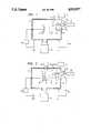
- FIG. 1is a schematic view showing an example of an apparatus by which the methods according to the present invention may be carried out.
- FIG. 2is a schematic view showing another example of another apparatus by which the methods according to the present invention can be carried out.
- FIG. 1is a schematic view showing an embodiment of the apparatus for carrying out the method according to the present invention.
- a vacuum vessel 8which is arranged to be exhausted by a vacuum pump 10 to form a vacuum therein, a holder 32 is provided to hold a substrate (for example, a base plate) 4, and an arc evaporation source 16 is provided opposite to the substrate 4.
- the arc evaporation source 16is provided with a cathode 18 made of carbon, a trigger electrode 20 for arc ignition, and a driving device 26 constituted by, for example, an air cylinder, or the like, for reciprocally moving the trigger electrode 20 through a feedthrough 22, in the direction as shown by arrow A, from the outside of the vacuum vessel 8.
- An arc power source 28 for applying a voltage of, for example, about several tens voltsis connected between the cathode 18 and the grounded vacuum vessel 8 so as to generate vaccum DC arc discharge between the cathode 18 and the vacuum vessel 8.
- the trigger electrode 20is connected to the earth through a resistor 24.
- a bias power source 34is connected between the holder 32 and the vacuum vessel 8 so as to apply a predetermined bias volt age, described later, to the substrate 4 (or to the holder 32 in the case where the substrate 4 is an insulating material.
- a selected gas Gis introduced from a gas source 14 into the vacuum vessel 8 through a gas leading inlet 12 provided through a wall of the vacuum vessel 8.
- the substrate 4which has been subjected to degreasing in advance is mounted on the holder 32, the inside of the vacuum vessel is exhausted, for example, to about 10 -5 -10 -7 Torr, hydrogen gas or an inert gas, such as argon or the like, is introduced as the gas G into the vacuum vessel 8 so that the pressure in the vacuum vessel 8 becomes about 0.1-several Torr, and then a negative bias voltage of about -50--1000V is applied to the substrate 4 from the bias power source 34 so as to generate glow discharge around the substrate 4. Accordingly, the gas G is ionized, and ions of the gas G are drawn to the substrate 4, which has a negative potential, so as to collide with the substrate 4 to cause contaminants on the substrate 4 to spatter by the collision energy and thereby cleanse the substrate 4.
- hydrogen gas or an inert gassuch as argon or the like
- the diamond filmis formed.
- a gas which may be hydrogen, an inert gas (such as argon, neon, or the like), a hydrocarbon series gas (such as methane, ethane or the like), and a gas of an organic compound series (such as acetone, or the like), or a mixture of two or more of the foregoing gasesis introduced as the gas G into the vacuum vessel 8, and the negative bias voltage is applied to the substrate 4 from the bias power source 34.
- Arc dischargeis generated by the arc evaporation source 16, so that carbon 30 evaporated from the arc evaporation source 16 is deposited on a surface of the substrate 4.
- the trigger electrode 20is separated from the cathode 18 after the trigger electrode 20 is caused to come into contact with the cathode 18 to thereby generate initial sparks, and the arc discharge is maintained between the cathode 18 and the vacuum vessel 8, so that the cathode 18 is heated and carbon 30 evaporated from the cathode 18.
- the carbon 30which is a cathode material, in the partially ionized state, is evaporated to the substrate 4 so as to deposit on the surface of the substrate 4.
- the gas Gis ionized by collision with the evaporated carbon ions and additionally by the glow discharge generated about the substrate 4, so that the thus produced gas ions are drawn by the substrate 4 having the negative potential so as to be caused to collide against the substrate 4.
- the collision ionsact as a nucleus forming energy supply source and cause the carbon to have a graphite structure, which upon being deposited on the substrate 4 grow into diamond crystals to thereby form a diamond film on the surface of the substrate 4.
- the reason for the selection of the gas, or gases, described above as the gas Gis that: (1) if hydrogen gas is used as the gas G, the hydrogen which has collided in the form of ions acts to remove graphite in the deposited carbon in the form of a hydrocarbon series gas such as methane, ethane or the like; (2) if a hydrocarbon series gas or a gas of an organic compound series is used as the gas G, ions of the same series as the deposited carbon, that is, carbon, collide with the deposited carbon, so that the deposited carbon is easily excited; (3) if an inert gas is used as the gas G, a high-quality diamond film containing no impurity therein can be obtained; and (4) if a mixture of the foregoing gases is used as the gas G, a combination of those actions described above can be obtained.
- the bias voltage to be applied to the substrate 4it is preferable to select the bias voltage to be applied to the substrate 4 to have a value within a range of about -50 to -1000 V, and more preferably within a range of about -50 to -600 V. This is because if the bias voltage is lower than about -1000 V, the ion acceleration energy becomes so large that the ion bombardment operation also becomes large, and not only is the diamond crystal growth badly influenced, but the deposition rate of diamond film is also lowered by spattering. On the other hand, if the bias voltage is higher than about -50V, not only does the ion drawing operation become extremely weak, but generation of the glow discharge about the substrate 4 becomes difficult.
- the substrate 4may be heated by heating means (not shown) to about several hundred °C. so that the reaction for diamond formation can be hastened by thermal excitation.
- the deposition of graphitecan be suppressed by the energy of the collision ions, so that a uniform diamond thin film can be obtained.
- the arc discharge at the carbon cathode 18is used for deposition of carbon, and it is not necessary to change the state of carbon from solid to liquid to pool the same, but the carbon is directly evaporated, so that the cathode 18, that is, the arc evaporation source 16 can be disposed in any position, upper side, lower side, left side or right side, in the vacuum vessel 8, and therefore a plurality of cathodes can be provided in parallel. Accordingly, the substraate 4 can be uniformly coated with a diamond film even if the substrate 4 has a large area and/or a complicated shape.
- a negative bias voltageis applid to the substrate 4 so that evaporated carbon ions and gas ions are accelerated and caused to collide against the substrate 4 to thereby form a film. Accordingly, the adhesion of the formed diamond film onto the substrate 4 is good.
- the second embodiment according to the present inventionwill be described next mainly with respect to the points differing from the first embodiment.
- a mixture of a first gas selected from hydrogen, inert gases, hydrocarbon series gases, gas of organic compound series or a mixture of two or more of the gases described above, and a second gas selected from silicon series gases (such as monosilane, disilane or the like) and a germanium series gas (such as germane, germanium fluoride or the like)is used as the gas G to be introduced into the vacuum vessel 8.
- silicon or germanium which is ionized and rushes into the deposited filmtakes only an SP 3 bond so as to suppress the deposition of graphite and to act effectively on the diamond formation.
- the mixing ratio of a gas of the silicon series and/or a gas of the germanium series to the first gas/gasesdoes not need to be large and the ratio is sufficient if it has a value within a range of, for example, from about 0.1% to about 30% (volume %).
- a higher-quality diamond filmcan be formed, in addition to the above features (1) to (5) of the first embodiment.
- thermoelectronswhen the substrate 4 is coated with a thick diamond film having a thickness of micron order, there is a possibility that the surface of the film will be charged positively (charged up) by collision ions, since a diamond film is an insulator and arc discharge is produced on the surface of the film to thereby damage the film. Accordingly, in that case, for example, as shown in FIG. 2, it is preferable to form a film while feeding thermoelectrons to the substrate 4 in such a manner, for example, that a filament 36 is provided in the vicinity of the substrate 4 and the filament 36 is heated by a power source 38 so as to emit thermoelectrons. Thus, the electrification on the film surface can be prevented by the thermoelectrons. In that case, as occasion demands, a bias for drawing the thermoelectrons may be applied between the filament 36 and the substrate 4.
- the deposition of carbon onto the substrate 4may be performed while high frequency discharge is being generated in a space between the substrate 4 and the cathode 18.
- a high frequency coilis used as the member 36 in FIG. 2 in place of the filament, and high frequency power is supplied to the high frequency coil from the power source 38 so as to generate high frequency discharge about the high frequency coil.
- ionization of the evaporated carbon 30 and the atmospheric gas Gis hastened, so that more strong ion energy can be used for diamond formation or the like.
- an AC bias voltageis applied to the substrate 4 from a bias power source 34.
- evaporated carbon ions and gas ionscan be accelerated toward the substrate 4, so that the energy of the accelerated ions can be used as a nucleus forming energy supply source similar to the case of the first embodiment to thereby form a diamond film on the surface of the substrate 4.
- secondary electrons emitted from the substrate 4 or the like by ion collisionare drawn back onto the substrate 4 or the like, so that the surface of the substrate 4 can be prevented from being charged up.
- the AC bias voltage applied to the substrate 4it is preferable for the AC bias voltage applied to the substrate 4 to have a peak value within a range of from about 50 V to about 1000 V, more preferably within a range of from about 50 V to about 600 V.
- the AC bias voltagemay have another waveform such as a square waveform, a saw tooth waveform, or a waveform composed of a part of a square wave.
- the third embodimenthas a further advantage that the surface of the diamond film can be prevented from being charged up even if thermoelectrons are not specially supplied to the substrate 4, in addition to the features (1) to (5) of the first embodiment.
- the fourth embodiment according to the present inventionwill be described next mainly with respect to the difference between it and the foregoing second embodiment.
- an AC bias voltageis applied to the substrate 4 from the bias power source 34 in forming a film. The operation is the same as described above.
- the fourth embodimenthas all the features of the first through third embodiments.
- carbon deposition onto the substrate 4may be performed while high frequency discharge is being generated in a space between the substrate 4 and the cathode 18. If it is desired that the electrification is more surely prevented, a film may be formed while thermoelectrons are being supplied to the substrate 4. The effects are as described above.
- a uniform filmcan be formed on a substrate even if the substrate has a large area and/or a complicated shape.
- the diamond filmcan be efficiently formed, and so on.
- thermoelectronsare not specially supplied onto the substrate, in addition to the effects (1) to (5).
- thermoelectronsare not specially supplied to the substrate, in addition to the foregoing benefits (1) to (5).
Landscapes
- Chemical & Material Sciences (AREA)
- Engineering & Computer Science (AREA)
- Materials Engineering (AREA)
- Metallurgy (AREA)
- Organic Chemistry (AREA)
- Crystallography & Structural Chemistry (AREA)
- Chemical Kinetics & Catalysis (AREA)
- Mechanical Engineering (AREA)
- Crystals, And After-Treatments Of Crystals (AREA)
Abstract
Description
Claims (10)
Applications Claiming Priority (2)
| Application Number | Priority Date | Filing Date | Title |
|---|---|---|---|
| JP62-43861 | 1987-02-26 | ||
| JP62043861AJPS63210099A (en) | 1987-02-26 | 1987-02-26 | Preparation of diamond film |
Publications (1)
| Publication Number | Publication Date |
|---|---|
| US4915977Atrue US4915977A (en) | 1990-04-10 |
Family
ID=12675479
Family Applications (1)
| Application Number | Title | Priority Date | Filing Date |
|---|---|---|---|
| US07/160,261Expired - LifetimeUS4915977A (en) | 1987-02-26 | 1988-02-25 | Method of forming a diamond film |
Country Status (4)
| Country | Link |
|---|---|
| US (1) | US4915977A (en) |
| EP (1) | EP0280315B1 (en) |
| JP (1) | JPS63210099A (en) |
| DE (1) | DE3881077T2 (en) |
Cited By (67)
| Publication number | Priority date | Publication date | Assignee | Title |
|---|---|---|---|---|
| US4997636A (en)* | 1989-02-16 | 1991-03-05 | Prins Johan F | Diamond growth |
| US5068871A (en)* | 1989-08-04 | 1991-11-26 | Kabushiki Kaisha Toyota Chuo Kenkyusho | Process for synthesizing diamond and apparatus therefor |
| US5070274A (en)* | 1989-03-20 | 1991-12-03 | Onoda Cement Company, Ltd. | Method for making diamond and apparatus therefor |
| US5071670A (en)* | 1990-06-11 | 1991-12-10 | Kelly Michael A | Method for chemical vapor deposition under a single reactor vessel divided into separate reaction chambers each with its own depositing and exhausting means |
| US5071708A (en)* | 1987-10-20 | 1991-12-10 | Showa Denko K.K. | Composite diamond grain |
| US5093151A (en)* | 1988-12-10 | 1992-03-03 | Fried, Krupp Gmbh | Plasma cvd process for coating a basic tool body |
| US5102687A (en)* | 1988-11-23 | 1992-04-07 | Centre National De La Recherche Scientifique-C.N.R.S. | Process for surface treatment by plasma of a substrate supported by an electrode |
| US5106452A (en)* | 1989-06-05 | 1992-04-21 | Semiconductor Energy Laboratory Co., Ltd. | Method of depositing diamond and diamond light emitting device |
| US5110577A (en)* | 1990-01-12 | 1992-05-05 | Ford Motor Company | Process of depositing a carbon film having metallic properties |
| US5132105A (en)* | 1990-02-02 | 1992-07-21 | Quantametrics, Inc. | Materials with diamond-like properties and method and means for manufacturing them |
| US5164051A (en)* | 1989-09-22 | 1992-11-17 | Showa Denko K. K. | Method for vapor phase synthesis of diamond on electrochemically treated substrate |
| US5173328A (en)* | 1988-12-10 | 1992-12-22 | Krupp Widia Gmbh | Plasma cvd process for coating a basic metallic body with a non-conductive coating material |
| US5182093A (en)* | 1990-01-08 | 1993-01-26 | Celestech, Inc. | Diamond deposition cell |
| US5190823A (en)* | 1989-07-31 | 1993-03-02 | General Electric Company | Method for improving adhesion of synthetic diamond coatings to substrates |
| US5201986A (en)* | 1990-08-07 | 1993-04-13 | Sumitomo Electric Industries, Ltd. | Diamond synthesizing method |
| US5221501A (en)* | 1991-06-11 | 1993-06-22 | The United States Of America As Represented By The Secretary Of Commerce | Method of producing a smooth plate of diamond |
| US5221411A (en)* | 1991-04-08 | 1993-06-22 | North Carolina State University | Method for synthesis and processing of continuous monocrystalline diamond thin films |
| US5223337A (en)* | 1988-12-10 | 1993-06-29 | Fried. Krupp Gmbh | Tool produced by a plasma-activated CVD process |
| US5227038A (en)* | 1991-10-04 | 1993-07-13 | William Marsh Rice University | Electric arc process for making fullerenes |
| US5260106A (en)* | 1990-08-03 | 1993-11-09 | Fujitsu Limited | Method for forming diamond films by plasma jet CVD |
| US5268201A (en)* | 1987-10-20 | 1993-12-07 | Showa Denko Kabushiki Kaisha | Composite diamond grain and method for production thereof |
| US5275850A (en)* | 1988-04-20 | 1994-01-04 | Hitachi, Ltd. | Process for producing a magnetic disk having a metal containing hard carbon coating by plasma chemical vapor deposition under a negative self bias |
| US5302231A (en)* | 1990-11-26 | 1994-04-12 | General Electric Company | CVD diamond by alternating chemical reactions |
| US5340401A (en)* | 1989-01-06 | 1994-08-23 | Celestech Inc. | Diamond deposition cell |
| US5352493A (en)* | 1991-05-03 | 1994-10-04 | Veniamin Dorfman | Method for forming diamond-like nanocomposite or doped-diamond-like nanocomposite films |
| US5397558A (en)* | 1991-03-26 | 1995-03-14 | Semiconductor Energy Laboratory Co., Ltd. | Method of forming diamond or diamond containing carbon film |
| US5397428A (en)* | 1991-12-20 | 1995-03-14 | The University Of North Carolina At Chapel Hill | Nucleation enhancement for chemical vapor deposition of diamond |
| US5425983A (en)* | 1992-08-10 | 1995-06-20 | Santa Barbara Research Center | Infrared window protected by multilayer antireflective coating |
| US5427827A (en)* | 1991-03-29 | 1995-06-27 | The United States Of America As Represented By The Administrator Of The National Aeronautics And Space Administration | Deposition of diamond-like films by ECR microwave plasma |
| US5433977A (en)* | 1993-05-21 | 1995-07-18 | Trustees Of Boston University | Enhanced adherence of diamond coatings by combustion flame CVD |
| US5458754A (en) | 1991-04-22 | 1995-10-17 | Multi-Arc Scientific Coatings | Plasma enhancement apparatus and method for physical vapor deposition |
| US5470661A (en)* | 1993-01-07 | 1995-11-28 | International Business Machines Corporation | Diamond-like carbon films from a hydrocarbon helium plasma |
| US5492770A (en)* | 1990-08-03 | 1996-02-20 | Fujitsu Limited | Method and apparatus for vapor deposition of diamond film |
| US5638251A (en)* | 1995-10-03 | 1997-06-10 | Advanced Refractory Technologies, Inc. | Capacitive thin films using diamond-like nanocomposite materials |
| US5674572A (en)* | 1993-05-21 | 1997-10-07 | Trustees Of Boston University | Enhanced adherence of diamond coatings employing pretreatment process |
| US5691010A (en)* | 1993-10-19 | 1997-11-25 | Sanyo Electric Co., Ltd. | Arc discharge plasma CVD method for forming diamond-like carbon films |
| US5695832A (en)* | 1993-07-07 | 1997-12-09 | Sanyo Electric Co., Ltd. | Method of forming a hard-carbon-film-coated substrate |
| US5707409A (en)* | 1994-08-24 | 1998-01-13 | Minnesota Mining And Manufacturing Company | Abrasive article having a diamond-like coating layer and method for making same |
| US5718976A (en)* | 1991-05-03 | 1998-02-17 | Advanced Refractory Technologies, Inc. | Erosion resistant diamond-like nanocomposite coatings for optical components |
| US5728465A (en)* | 1991-05-03 | 1998-03-17 | Advanced Refractory Technologies, Inc. | Diamond-like nanocomposite corrosion resistant coatings |
| US5786068A (en)* | 1991-05-03 | 1998-07-28 | Advanced Refractory Technologies, Inc. | Electrically tunable coatings |
| US5795648A (en)* | 1995-10-03 | 1998-08-18 | Advanced Refractory Technologies, Inc. | Method for preserving precision edges using diamond-like nanocomposite film coatings |
| WO1998041666A1 (en)* | 1997-03-20 | 1998-09-24 | Motorola Inc. | Method for forming a carbon film |
| US6013980A (en)* | 1997-05-09 | 2000-01-11 | Advanced Refractory Technologies, Inc. | Electrically tunable low secondary electron emission diamond-like coatings and process for depositing coatings |
| WO2002006554A1 (en)* | 2000-07-17 | 2002-01-24 | Commonwealth Scientific And Industrial Research Organisation | Deposition of carbon and carbon-based materials |
| US6468642B1 (en) | 1995-10-03 | 2002-10-22 | N.V. Bekaert S.A. | Fluorine-doped diamond-like coatings |
| US6572936B1 (en)* | 1996-06-09 | 2003-06-03 | Sanyo Electric Co., Ltd. | Hard carbon film-coated substrate and method for fabricating the same |
| US6579428B2 (en)* | 2000-09-26 | 2003-06-17 | Shinmaywa Industries, Ltd. | Arc evaporator, method for driving arc evaporator, and ion plating apparatus |
| US6660365B1 (en) | 1998-12-21 | 2003-12-09 | Cardinal Cg Company | Soil-resistant coating for glass surfaces |
| US6660329B2 (en) | 2001-09-05 | 2003-12-09 | Kennametal Inc. | Method for making diamond coated cutting tool |
| US20050016835A1 (en)* | 1998-12-21 | 2005-01-27 | Cardinal Cg Company | Soil-resistant coating for glass surfaces |
| RU2250874C1 (en)* | 2002-09-10 | 2005-04-27 | Хоккайдо Юниверсити | Method of production of diamond |
| US20050137084A1 (en)* | 2003-12-22 | 2005-06-23 | Krisko Annette J. | Graded photocatalytic coatings |
| US6974629B1 (en) | 1999-08-06 | 2005-12-13 | Cardinal Cg Company | Low-emissivity, soil-resistant coating for glass surfaces |
| US20060057298A1 (en)* | 2004-07-12 | 2006-03-16 | Krisko Annette J | Low-maintenance coatings |
| US20060121315A1 (en)* | 2004-12-03 | 2006-06-08 | Kari Myli | Hydrophilic coatings, methods for depositing hydrophilic coatings, and improved deposition technology for thin films |
| US20060118408A1 (en)* | 2004-12-03 | 2006-06-08 | Kari Myli | Methods and equipment for depositing hydrophilic coatings, and deposition technologies for thin films |
| US20070193518A1 (en)* | 2004-03-16 | 2007-08-23 | Ferrotec Corporation And Hirofumi Takikawa | Plasma generator |
| US20070248756A1 (en)* | 2006-04-19 | 2007-10-25 | Cardinal Cg Company | Opposed functional coatings having comparable single surface reflectances |
| US20080045112A1 (en)* | 1994-08-29 | 2008-02-21 | Canon Kabushiki Kaisha | Method for manufacturing an electron-emitting device with first and second carbon films |
| US7473410B1 (en) | 1990-08-30 | 2009-01-06 | Mitsubishi Corporation | Form of carbon |
| CN101806928A (en)* | 2010-03-31 | 2010-08-18 | 西安交通大学 | Hard resin lens and organic glass lens surface ultra-hard coat coating method |
| US20100326817A1 (en)* | 2007-09-14 | 2010-12-30 | Cardinal Cg Company | Low-maintenance coatings, and methods for producing low-maintenance coatings |
| US9738967B2 (en) | 2006-07-12 | 2017-08-22 | Cardinal Cg Company | Sputtering apparatus including target mounting and control |
| US10604442B2 (en) | 2016-11-17 | 2020-03-31 | Cardinal Cg Company | Static-dissipative coating technology |
| CN116970902A (en)* | 2023-06-19 | 2023-10-31 | 广东工业大学 | Diamond-like coating and preparation method and application thereof |
| US12084777B2 (en)* | 2017-09-25 | 2024-09-10 | Sumitomo Electric Industries, Ltd. | Method for manufacturing hard carbon-based coating, and member provided with coating |
Families Citing this family (8)
| Publication number | Priority date | Publication date | Assignee | Title |
|---|---|---|---|---|
| US5296274A (en)* | 1989-05-10 | 1994-03-22 | Movchan Boris A | Method of producing carbon-containing materials by electron beam vacuum evaporation of graphite and subsequent condensation |
| JPH03122091A (en)* | 1989-09-29 | 1991-05-24 | Natl Inst For Res In Inorg Mater | Rapid synthesis method of diamond |
| DE3941202A1 (en)* | 1989-12-14 | 1990-06-07 | Fried. Krupp Gmbh, 4300 Essen | METHOD FOR PRODUCING LAYERS FROM HARD CARBON MODIFICATIONS AND DEVICE FOR IMPLEMENTING THE METHOD |
| FR2670218B1 (en)* | 1990-12-06 | 1993-02-05 | Innovatique Sa | PROCESS FOR TREATING METALS BY DEPOSIT OF MATERIAL, AND FOR CARRYING OUT SAID METHOD. |
| DE4233085C2 (en) | 1992-10-01 | 1996-10-10 | Fraunhofer Ges Forschung | Process for producing heteroepitaxial diamond layers |
| US5401543A (en)* | 1993-11-09 | 1995-03-28 | Minnesota Mining And Manufacturing Company | Method for forming macroparticle-free DLC films by cathodic arc discharge |
| WO1995027806A1 (en)* | 1994-04-06 | 1995-10-19 | The Regents Of The University Of California | Process to produce diamond films |
| US5837331A (en)* | 1996-03-13 | 1998-11-17 | Motorola, Inc. | Amorphous multi-layered structure and method of making the same |
Citations (8)
| Publication number | Priority date | Publication date | Assignee | Title |
|---|---|---|---|---|
| GB1395648A (en)* | 1972-05-18 | 1975-05-29 | Standard Telephones Cables Ltd | Diamond synthesis |
| US3961103A (en)* | 1972-07-12 | 1976-06-01 | Space Sciences, Inc. | Film deposition |
| US4228142A (en)* | 1979-08-31 | 1980-10-14 | Holcombe Cressie E Jun | Process for producing diamond-like carbon |
| US4490229A (en)* | 1984-07-09 | 1984-12-25 | The United States Of America As Represented By The Administrator Of The National Aeronautics And Space Administration | Deposition of diamondlike carbon films |
| JPS60118693A (en)* | 1983-11-25 | 1985-06-26 | Mitsubishi Metal Corp | Low-pressure diamond synthesis method |
| JPS60171294A (en)* | 1984-02-13 | 1985-09-04 | Mitsubishi Metal Corp | How to produce artificial diamond by vapor deposition |
| US4725345A (en)* | 1985-04-22 | 1988-02-16 | Kabushiki Kaisha Kenwood | Method for forming a hard carbon thin film on article and applications thereof |
| US4767608A (en)* | 1986-10-23 | 1988-08-30 | National Institute For Research In Inorganic Materials | Method for synthesizing diamond by using plasma |
Family Cites Families (1)
| Publication number | Priority date | Publication date | Assignee | Title |
|---|---|---|---|---|
| US4437962A (en)* | 1983-05-17 | 1984-03-20 | The United States Of America As Represented By The Administrator Of The National Aeronautics And Space Administration | Diamondlike flake composites |
- 1987
- 1987-02-26JPJP62043861Apatent/JPS63210099A/enactivePending
- 1988
- 1988-02-25USUS07/160,261patent/US4915977A/ennot_activeExpired - Lifetime
- 1988-02-25DEDE8888102852Tpatent/DE3881077T2/ennot_activeExpired - Fee Related
- 1988-02-25EPEP88102852Apatent/EP0280315B1/ennot_activeExpired - Lifetime
Patent Citations (8)
| Publication number | Priority date | Publication date | Assignee | Title |
|---|---|---|---|---|
| GB1395648A (en)* | 1972-05-18 | 1975-05-29 | Standard Telephones Cables Ltd | Diamond synthesis |
| US3961103A (en)* | 1972-07-12 | 1976-06-01 | Space Sciences, Inc. | Film deposition |
| US4228142A (en)* | 1979-08-31 | 1980-10-14 | Holcombe Cressie E Jun | Process for producing diamond-like carbon |
| JPS60118693A (en)* | 1983-11-25 | 1985-06-26 | Mitsubishi Metal Corp | Low-pressure diamond synthesis method |
| JPS60171294A (en)* | 1984-02-13 | 1985-09-04 | Mitsubishi Metal Corp | How to produce artificial diamond by vapor deposition |
| US4490229A (en)* | 1984-07-09 | 1984-12-25 | The United States Of America As Represented By The Administrator Of The National Aeronautics And Space Administration | Deposition of diamondlike carbon films |
| US4725345A (en)* | 1985-04-22 | 1988-02-16 | Kabushiki Kaisha Kenwood | Method for forming a hard carbon thin film on article and applications thereof |
| US4767608A (en)* | 1986-10-23 | 1988-08-30 | National Institute For Research In Inorganic Materials | Method for synthesizing diamond by using plasma |
Cited By (101)
| Publication number | Priority date | Publication date | Assignee | Title |
|---|---|---|---|---|
| US5268201A (en)* | 1987-10-20 | 1993-12-07 | Showa Denko Kabushiki Kaisha | Composite diamond grain and method for production thereof |
| US5071708A (en)* | 1987-10-20 | 1991-12-10 | Showa Denko K.K. | Composite diamond grain |
| US5275850A (en)* | 1988-04-20 | 1994-01-04 | Hitachi, Ltd. | Process for producing a magnetic disk having a metal containing hard carbon coating by plasma chemical vapor deposition under a negative self bias |
| US5102687A (en)* | 1988-11-23 | 1992-04-07 | Centre National De La Recherche Scientifique-C.N.R.S. | Process for surface treatment by plasma of a substrate supported by an electrode |
| US5223337A (en)* | 1988-12-10 | 1993-06-29 | Fried. Krupp Gmbh | Tool produced by a plasma-activated CVD process |
| US5173328A (en)* | 1988-12-10 | 1992-12-22 | Krupp Widia Gmbh | Plasma cvd process for coating a basic metallic body with a non-conductive coating material |
| US5093151A (en)* | 1988-12-10 | 1992-03-03 | Fried, Krupp Gmbh | Plasma cvd process for coating a basic tool body |
| US5340401A (en)* | 1989-01-06 | 1994-08-23 | Celestech Inc. | Diamond deposition cell |
| US4997636A (en)* | 1989-02-16 | 1991-03-05 | Prins Johan F | Diamond growth |
| US5070274A (en)* | 1989-03-20 | 1991-12-03 | Onoda Cement Company, Ltd. | Method for making diamond and apparatus therefor |
| US5106452A (en)* | 1989-06-05 | 1992-04-21 | Semiconductor Energy Laboratory Co., Ltd. | Method of depositing diamond and diamond light emitting device |
| US5190823A (en)* | 1989-07-31 | 1993-03-02 | General Electric Company | Method for improving adhesion of synthetic diamond coatings to substrates |
| US5068871A (en)* | 1989-08-04 | 1991-11-26 | Kabushiki Kaisha Toyota Chuo Kenkyusho | Process for synthesizing diamond and apparatus therefor |
| US5164051A (en)* | 1989-09-22 | 1992-11-17 | Showa Denko K. K. | Method for vapor phase synthesis of diamond on electrochemically treated substrate |
| US5182093A (en)* | 1990-01-08 | 1993-01-26 | Celestech, Inc. | Diamond deposition cell |
| US5110577A (en)* | 1990-01-12 | 1992-05-05 | Ford Motor Company | Process of depositing a carbon film having metallic properties |
| US5132105A (en)* | 1990-02-02 | 1992-07-21 | Quantametrics, Inc. | Materials with diamond-like properties and method and means for manufacturing them |
| US5071670A (en)* | 1990-06-11 | 1991-12-10 | Kelly Michael A | Method for chemical vapor deposition under a single reactor vessel divided into separate reaction chambers each with its own depositing and exhausting means |
| US5492770A (en)* | 1990-08-03 | 1996-02-20 | Fujitsu Limited | Method and apparatus for vapor deposition of diamond film |
| US5260106A (en)* | 1990-08-03 | 1993-11-09 | Fujitsu Limited | Method for forming diamond films by plasma jet CVD |
| US5201986A (en)* | 1990-08-07 | 1993-04-13 | Sumitomo Electric Industries, Ltd. | Diamond synthesizing method |
| US7473410B1 (en) | 1990-08-30 | 2009-01-06 | Mitsubishi Corporation | Form of carbon |
| US8101149B1 (en) | 1990-08-30 | 2012-01-24 | Mitsubishi Corporation | Form of carbon |
| US7976813B1 (en) | 1990-08-30 | 2011-07-12 | Mitsubishi Corporation | Form of carbon |
| US5302231A (en)* | 1990-11-26 | 1994-04-12 | General Electric Company | CVD diamond by alternating chemical reactions |
| US5397558A (en)* | 1991-03-26 | 1995-03-14 | Semiconductor Energy Laboratory Co., Ltd. | Method of forming diamond or diamond containing carbon film |
| US5427827A (en)* | 1991-03-29 | 1995-06-27 | The United States Of America As Represented By The Administrator Of The National Aeronautics And Space Administration | Deposition of diamond-like films by ECR microwave plasma |
| US5221411A (en)* | 1991-04-08 | 1993-06-22 | North Carolina State University | Method for synthesis and processing of continuous monocrystalline diamond thin films |
| US6139964A (en) | 1991-04-22 | 2000-10-31 | Multi-Arc Inc. | Plasma enhancement apparatus and method for physical vapor deposition |
| US5458754A (en) | 1991-04-22 | 1995-10-17 | Multi-Arc Scientific Coatings | Plasma enhancement apparatus and method for physical vapor deposition |
| US5352493A (en)* | 1991-05-03 | 1994-10-04 | Veniamin Dorfman | Method for forming diamond-like nanocomposite or doped-diamond-like nanocomposite films |
| US5718976A (en)* | 1991-05-03 | 1998-02-17 | Advanced Refractory Technologies, Inc. | Erosion resistant diamond-like nanocomposite coatings for optical components |
| US5466431A (en)* | 1991-05-03 | 1995-11-14 | Veniamin Dorfman | Diamond-like metallic nanocomposites |
| US5786068A (en)* | 1991-05-03 | 1998-07-28 | Advanced Refractory Technologies, Inc. | Electrically tunable coatings |
| US5728465A (en)* | 1991-05-03 | 1998-03-17 | Advanced Refractory Technologies, Inc. | Diamond-like nanocomposite corrosion resistant coatings |
| US5221501A (en)* | 1991-06-11 | 1993-06-22 | The United States Of America As Represented By The Secretary Of Commerce | Method of producing a smooth plate of diamond |
| US5227038A (en)* | 1991-10-04 | 1993-07-13 | William Marsh Rice University | Electric arc process for making fullerenes |
| US5397428A (en)* | 1991-12-20 | 1995-03-14 | The University Of North Carolina At Chapel Hill | Nucleation enhancement for chemical vapor deposition of diamond |
| US5420443A (en)* | 1991-12-20 | 1995-05-30 | Kobe Development Corporation | Microelectronic structure having an array of diamond structures on a nondiamond substrate and associated fabrication methods |
| US5425983A (en)* | 1992-08-10 | 1995-06-20 | Santa Barbara Research Center | Infrared window protected by multilayer antireflective coating |
| US5569501A (en)* | 1993-01-07 | 1996-10-29 | International Business Machines Corporation | Diamond-like carbon films from a hydrocarbon helium plasma |
| US5470661A (en)* | 1993-01-07 | 1995-11-28 | International Business Machines Corporation | Diamond-like carbon films from a hydrocarbon helium plasma |
| US5674572A (en)* | 1993-05-21 | 1997-10-07 | Trustees Of Boston University | Enhanced adherence of diamond coatings employing pretreatment process |
| US5491028A (en)* | 1993-05-21 | 1996-02-13 | Trustees Of Boston University | Enhanced adherence of diamond coatings |
| US5433977A (en)* | 1993-05-21 | 1995-07-18 | Trustees Of Boston University | Enhanced adherence of diamond coatings by combustion flame CVD |
| US5695832A (en)* | 1993-07-07 | 1997-12-09 | Sanyo Electric Co., Ltd. | Method of forming a hard-carbon-film-coated substrate |
| US5691010A (en)* | 1993-10-19 | 1997-11-25 | Sanyo Electric Co., Ltd. | Arc discharge plasma CVD method for forming diamond-like carbon films |
| US5707409A (en)* | 1994-08-24 | 1998-01-13 | Minnesota Mining And Manufacturing Company | Abrasive article having a diamond-like coating layer and method for making same |
| US20080045112A1 (en)* | 1994-08-29 | 2008-02-21 | Canon Kabushiki Kaisha | Method for manufacturing an electron-emitting device with first and second carbon films |
| US7758762B2 (en) | 1994-08-29 | 2010-07-20 | Canon Kabushiki Kaisha | Method for manufacturing an electron-emitting device with first and second carbon films |
| US6468642B1 (en) | 1995-10-03 | 2002-10-22 | N.V. Bekaert S.A. | Fluorine-doped diamond-like coatings |
| US5795648A (en)* | 1995-10-03 | 1998-08-18 | Advanced Refractory Technologies, Inc. | Method for preserving precision edges using diamond-like nanocomposite film coatings |
| US5638251A (en)* | 1995-10-03 | 1997-06-10 | Advanced Refractory Technologies, Inc. | Capacitive thin films using diamond-like nanocomposite materials |
| US6572936B1 (en)* | 1996-06-09 | 2003-06-03 | Sanyo Electric Co., Ltd. | Hard carbon film-coated substrate and method for fabricating the same |
| WO1998041666A1 (en)* | 1997-03-20 | 1998-09-24 | Motorola Inc. | Method for forming a carbon film |
| US6486597B1 (en) | 1997-05-09 | 2002-11-26 | N.V. Bekaert S.A. | Electrically tunable low secondary electron emission diamond-like coatings and process for depositing coatings |
| US6013980A (en)* | 1997-05-09 | 2000-01-11 | Advanced Refractory Technologies, Inc. | Electrically tunable low secondary electron emission diamond-like coatings and process for depositing coatings |
| US7491301B2 (en) | 1998-12-21 | 2009-02-17 | Cardinal Cg Company | Methods and apparatuses for depositing film on both sides of a pane |
| US20050016835A1 (en)* | 1998-12-21 | 2005-01-27 | Cardinal Cg Company | Soil-resistant coating for glass surfaces |
| US20050025982A1 (en)* | 1998-12-21 | 2005-02-03 | Cardinal Cg Company | Soil-resistant coating for glass surfaces |
| US20060115655A1 (en)* | 1998-12-21 | 2006-06-01 | Krisko Annette J | Low-emissivity, soil-resistant coating for glass surfaces |
| US6660365B1 (en) | 1998-12-21 | 2003-12-09 | Cardinal Cg Company | Soil-resistant coating for glass surfaces |
| US6939446B2 (en) | 1998-12-21 | 2005-09-06 | Cardinal Cg Company | Soil-resistant coating for glass surfaces |
| US6964731B1 (en) | 1998-12-21 | 2005-11-15 | Cardinal Cg Company | Soil-resistant coating for glass surfaces |
| US20060000706A1 (en)* | 1998-12-21 | 2006-01-05 | Cardinal Cg Company | Soil-resistant coating for glass surfaces |
| US20030228431A1 (en)* | 1998-12-21 | 2003-12-11 | Annette Krisko | Soil-resistant coating for glass surfaces |
| US7294403B2 (en) | 1998-12-21 | 2007-11-13 | Cardinal Cg Company | Soil-resistant coating for glass surfaces |
| US6974629B1 (en) | 1999-08-06 | 2005-12-13 | Cardinal Cg Company | Low-emissivity, soil-resistant coating for glass surfaces |
| US20030234176A1 (en)* | 2000-07-17 | 2003-12-25 | Jawad Haidar | Production of carbon and carbon-based materials |
| WO2002006554A1 (en)* | 2000-07-17 | 2002-01-24 | Commonwealth Scientific And Industrial Research Organisation | Deposition of carbon and carbon-based materials |
| KR100807374B1 (en)* | 2000-09-26 | 2008-02-28 | 신메이와 인더스트리즈,리미티드 | Arc Evaporator, Method for Driving Arc Evaporator, and Ion Plating Apparatus |
| US6579428B2 (en)* | 2000-09-26 | 2003-06-17 | Shinmaywa Industries, Ltd. | Arc evaporator, method for driving arc evaporator, and ion plating apparatus |
| US6890655B2 (en) | 2001-09-05 | 2005-05-10 | Kennametal Inc. | Diamond coated cutting tool and method for making the same |
| US20040028892A1 (en)* | 2001-09-05 | 2004-02-12 | Yixiong Liu | Diamond coated cutting tool and method for making the same |
| US6660329B2 (en) | 2001-09-05 | 2003-12-09 | Kennametal Inc. | Method for making diamond coated cutting tool |
| RU2250874C1 (en)* | 2002-09-10 | 2005-04-27 | Хоккайдо Юниверсити | Method of production of diamond |
| US7294404B2 (en) | 2003-12-22 | 2007-11-13 | Cardinal Cg Company | Graded photocatalytic coatings |
| US20050137084A1 (en)* | 2003-12-22 | 2005-06-23 | Krisko Annette J. | Graded photocatalytic coatings |
| US20070193518A1 (en)* | 2004-03-16 | 2007-08-23 | Ferrotec Corporation And Hirofumi Takikawa | Plasma generator |
| US7823537B2 (en)* | 2004-03-16 | 2010-11-02 | Ferrotec Corporation | Plasma generator |
| US20060057298A1 (en)* | 2004-07-12 | 2006-03-16 | Krisko Annette J | Low-maintenance coatings |
| USRE43817E1 (en) | 2004-07-12 | 2012-11-20 | Cardinal Cg Company | Low-maintenance coatings |
| US7713632B2 (en) | 2004-07-12 | 2010-05-11 | Cardinal Cg Company | Low-maintenance coatings |
| US7604865B2 (en) | 2004-07-12 | 2009-10-20 | Cardinal Cg Company | Low-maintenance coatings |
| US20060057401A1 (en)* | 2004-07-12 | 2006-03-16 | Krisko Annette J | Low-maintenance coatings |
| USRE44155E1 (en) | 2004-07-12 | 2013-04-16 | Cardinal Cg Company | Low-maintenance coatings |
| US20060121315A1 (en)* | 2004-12-03 | 2006-06-08 | Kari Myli | Hydrophilic coatings, methods for depositing hydrophilic coatings, and improved deposition technology for thin films |
| US7923114B2 (en) | 2004-12-03 | 2011-04-12 | Cardinal Cg Company | Hydrophilic coatings, methods for depositing hydrophilic coatings, and improved deposition technology for thin films |
| US8092660B2 (en) | 2004-12-03 | 2012-01-10 | Cardinal Cg Company | Methods and equipment for depositing hydrophilic coatings, and deposition technologies for thin films |
| US20060118408A1 (en)* | 2004-12-03 | 2006-06-08 | Kari Myli | Methods and equipment for depositing hydrophilic coatings, and deposition technologies for thin films |
| US20070248756A1 (en)* | 2006-04-19 | 2007-10-25 | Cardinal Cg Company | Opposed functional coatings having comparable single surface reflectances |
| US7989094B2 (en) | 2006-04-19 | 2011-08-02 | Cardinal Cg Company | Opposed functional coatings having comparable single surface reflectances |
| US9738967B2 (en) | 2006-07-12 | 2017-08-22 | Cardinal Cg Company | Sputtering apparatus including target mounting and control |
| US20100326817A1 (en)* | 2007-09-14 | 2010-12-30 | Cardinal Cg Company | Low-maintenance coatings, and methods for producing low-maintenance coatings |
| US8506768B2 (en) | 2007-09-14 | 2013-08-13 | Cardinal Cg Company | Low-maintenance coatings, and methods for producing low-maintenance coatings |
| US8696879B2 (en) | 2007-09-14 | 2014-04-15 | Cardinal Cg Company | Low-maintenance coating technology |
| CN101806928A (en)* | 2010-03-31 | 2010-08-18 | 西安交通大学 | Hard resin lens and organic glass lens surface ultra-hard coat coating method |
| US10604442B2 (en) | 2016-11-17 | 2020-03-31 | Cardinal Cg Company | Static-dissipative coating technology |
| US11325859B2 (en) | 2016-11-17 | 2022-05-10 | Cardinal Cg Company | Static-dissipative coating technology |
| US12084777B2 (en)* | 2017-09-25 | 2024-09-10 | Sumitomo Electric Industries, Ltd. | Method for manufacturing hard carbon-based coating, and member provided with coating |
| CN116970902A (en)* | 2023-06-19 | 2023-10-31 | 广东工业大学 | Diamond-like coating and preparation method and application thereof |
Also Published As
| Publication number | Publication date |
|---|---|
| EP0280315A2 (en) | 1988-08-31 |
| JPS63210099A (en) | 1988-08-31 |
| EP0280315A3 (en) | 1989-07-19 |
| DE3881077D1 (en) | 1993-06-24 |
| EP0280315B1 (en) | 1993-05-19 |
| DE3881077T2 (en) | 1993-09-02 |
Similar Documents
| Publication | Publication Date | Title |
|---|---|---|
| US4915977A (en) | Method of forming a diamond film | |
| CA1308689C (en) | Method and apparatus for forming a thin film | |
| EP0253361B1 (en) | Thin film forming device | |
| US4799454A (en) | Apparatus for forming a thin film | |
| US4986214A (en) | Thin film forming apparatus | |
| JPH0635323B2 (en) | Surface treatment method | |
| JP3386175B2 (en) | Method of forming compound thin film with gas cluster ion assist | |
| US4798739A (en) | Plasma-assisted method for thin film fabrication | |
| US5378285A (en) | Apparatus for forming a diamond-like thin film | |
| US3492215A (en) | Sputtering of material simultaneously evaporated onto the target | |
| JPS644591B2 (en) | ||
| JPS60251269A (en) | Method and apparatus for ionic plating | |
| JPH06220621A (en) | Device for forming film by sputtering | |
| US6223686B1 (en) | Apparatus for forming a thin film by plasma chemical vapor deposition | |
| JP3246780B2 (en) | Method and apparatus for forming hard carbon film | |
| KR900008155B1 (en) | Thin film formation method and apparatus | |
| EP0280198A1 (en) | Method of forming diamond film | |
| JP2893992B2 (en) | Method and apparatus for synthesizing hard carbon film | |
| JPS63458A (en) | Vacuum arc vapor deposition device | |
| JP2848590B1 (en) | Electron beam excited plasma generator | |
| JPH0779085B2 (en) | Compound thin film forming equipment | |
| JPH0751750B2 (en) | Film forming equipment | |
| CA1305564C (en) | Substrate cleaning device | |
| JP2002313736A (en) | Plasma treating equipment | |
| JPH07335395A (en) | Plasma generation method and film forming method, etching method, semiconductor deposition method and doping method using the same |
Legal Events
| Date | Code | Title | Description |
|---|---|---|---|
| AS | Assignment | Owner name:NISSIN ELECTRIC CO., LTD., NO. 47, UMEZU TAKASE-CH Free format text:ASSIGNMENT OF ASSIGNORS INTEREST.;ASSIGNORS:OKAMOTO, KOJI;TANJO, MASAYASU;KAMIJO, EIJI;REEL/FRAME:004892/0666 Effective date:19880418 Owner name:NISSIN ELECTRIC CO., LTD., JAPAN Free format text:ASSIGNMENT OF ASSIGNORS INTEREST;ASSIGNORS:OKAMOTO, KOJI;TANJO, MASAYASU;KAMIJO, EIJI;REEL/FRAME:004892/0666 Effective date:19880418 | |
| STCF | Information on status: patent grant | Free format text:PATENTED CASE | |
| FEPP | Fee payment procedure | Free format text:PAYOR NUMBER ASSIGNED (ORIGINAL EVENT CODE: ASPN); ENTITY STATUS OF PATENT OWNER: LARGE ENTITY | |
| FPAY | Fee payment | Year of fee payment:4 | |
| FPAY | Fee payment | Year of fee payment:8 | |
| FEPP | Fee payment procedure | Free format text:PAYER NUMBER DE-ASSIGNED (ORIGINAL EVENT CODE: RMPN); ENTITY STATUS OF PATENT OWNER: LARGE ENTITY Free format text:PAYOR NUMBER ASSIGNED (ORIGINAL EVENT CODE: ASPN); ENTITY STATUS OF PATENT OWNER: LARGE ENTITY | |
| FPAY | Fee payment | Year of fee payment:12 |