US4912631A - Burst mode cache with wrap-around fill - Google Patents
Burst mode cache with wrap-around fillDownload PDFInfo
- Publication number
- US4912631A US4912631AUS07/133,529US13352987AUS4912631AUS 4912631 AUS4912631 AUS 4912631AUS 13352987 AUS13352987 AUS 13352987AUS 4912631 AUS4912631 AUS 4912631A
- Authority
- US
- United States
- Prior art keywords
- cache
- words
- processing unit
- word
- data
- Prior art date
- Legal status (The legal status is an assumption and is not a legal conclusion. Google has not performed a legal analysis and makes no representation as to the accuracy of the status listed.)
- Expired - Lifetime
Links
Images


Classifications
- G—PHYSICS
- G06—COMPUTING OR CALCULATING; COUNTING
- G06F—ELECTRIC DIGITAL DATA PROCESSING
- G06F12/00—Accessing, addressing or allocating within memory systems or architectures
- G06F12/02—Addressing or allocation; Relocation
- G06F12/08—Addressing or allocation; Relocation in hierarchically structured memory systems, e.g. virtual memory systems
- G06F12/0802—Addressing of a memory level in which the access to the desired data or data block requires associative addressing means, e.g. caches
- G06F12/0877—Cache access modes
- G06F12/0879—Burst mode
Definitions
- the present inventionrelates to data processing systems and more particularly, to a method and apparatus for controlling data transfers between a data processing unit and a cache.
- a cacheis a relatively high-speed, small, local memory which is used to provide a local storage for frequently accessed memory locations of a larger, relatively slow, main memory.
- the cacheBy storing a duplicate copy of the most frequently used main memory information locally, the cache is able to rapidly respond to most memory references, thus avoiding the accessing of the slower main memory. The result is lower traffic on the memory bus and decreased latency on the local bus to the requesting data processing unit.
- the use of a cachealso increases potential systems' performance by reducing each data processing unit's demand for system bus bandwidth, thus allowing more data processing units in the system.
- a cache configuration registersplits the cache directory into two or more logical directories which are able to control requests from two or more data processing units.
- the cachewill have to arbitrate for the bus in order to prevent the data processing unit from beginning another access while the cache is being updated. This would improve access latency, but would still decrease bus bandwidth.
- the data processing unitmay attempt another access before the cache is completely updated. For example, consider the situation where the data processing unit requests only the first word of the four-word line. The update of the cache line requires all four words, so while the last three words are being transferred to the cache only, the data processing unit may try to access the memory.
- the above objectis accomplished in accordance with the invention by a method and apparatus of updating a cache backed by a main memory.
- Multiple word data transferstake place between the cache and the data processing unit if data is in the cache, and between the main memory and the data processing unit if data is not in the cache.
- kis the address of the first word requested
- nis the address of the last word requested.
- the transfertakes place by first determining if the requested data words (k through n) reside in the cache.
- the requested words (k through n)are transferred from the cache to the data processing unit. If they do not reside in the cache, then the cache is updated by transferring the requested words (k through n) simultaneously from the main memory to the cache and from the main memory to the data processing unit. This cache update is accomplished by first writing the last words of the line containing the requested words only to the cache (starting at word n+1 and ending at word k-1) and then writing the remaining words comprising the requested words (k thrugh n) to the cache and the data processing unit simultaneously (starting at word k and ending at word n).
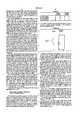
- FIG. 1is a block diagram of a data processing system in which the present invention is embodied
- FIG. 2is a timing diagram illustrating the order of access of words transferred by the prior art apparatus.
- FIG. 3is a timing diagram illustrating the order of access of words transferred by the apparatus of FIG. 1.
- FIG. 1is a block diagram of a data processing system in which the present invention is embodied.
- the systemis comprised of a cache (10) which is a high-speed local store which duplicates most recently used information stored in slower main memory (12).
- the cacheis used as an intermediate high-speed memory between the main memory and a generalized data processing unit (GDP-14).
- GDP-14generalized data processing unit
- a cache controller (CC-16)is provided to control access to the cache (10) and a memory control unit (MCU-20) is provided to control access to the main memory (12).
- Communication between the GDP, cache controller (14) and MCU (20)is over an address/data bus (23) interconnecting the units.
- a searchis made of a cache directory (18) in the cache controller to see if the information is in the cache. If it is, a main memory reference is avoided, since the data requested can be transferred from the cache. If the data is not in the cache, a main memory access is initiated and the data is transferred to the cache controller (16) and the GDP interface (15) over the bus (23).
- Both the cache controller (16) and the MCU (20)contain a programmable logic array (PLA). Each PLA (21 and 25) controls the data transfer in accordance with an identical programmed access algorithm.
- the access algorithmprovides that during a cache update, the order of access of requested words is altered, so that the non-requested words are transferred to the cache first, and then the requested words are transferred simultaneously to the cache and GDP.
- the GDPwill not attempt a new data transfer via its memory access interface (15) until it receives the requested words. Since the order of transfer is changed, the GDP (14) receives the requested words after the cache (10) is updated with the non-requested words. This prevents a GDP access during the update of the cache.
- FIG. 2is timing diagram of the prior art access method described in the above-identified Johnson, et al. application.
- the cache line(four words) is first updated with the new data (32) from memory, word 2, word 3, word 4, word 1 on the data bus, and then the requested data (34), word 2, word 3, on the data bus, is transferred from the cache to the GDP. This automatically results in four additional wait states (32) for the GDP access in addition to any memory-latency-wait states.
- FIG. 3is a timing diagram illustrating the same access request using the method of the present invention.
- a request (40) for two words (word 2, word 3)the transfer takes place by first determining if the requested data words reside in the cache. If they do, then the requested words are transferred from the cache to the GDP and no cache update is necessary. If they do not, then the requested words are transferred by first writing the last two words (42) of the line to the cache only, word 4, word 1, by asserting the cache ready line (46) while deasserting the processor ready line (48). The reamining two words (44) comprising the requested words, word 2 and word 3, are then written to the GDP as well as the cache, by asserting the processor ready line (48).
- the above-described methodis accomplished by utilizing two pieces of information, which are placed on the bus (23) by the GDP: the data word's offset and the number of words requested.
- the first words (n+1 through k-1)are written to the cache only.
- the last words (k through n)are transferred simultaneously to the cache and GDP. For a four-word access, four wait states are saved.
- the programmable logic array (PLA) algorithm for accomplishing thisis listed below.
- the PLA (21) in the cache controlleris identical to the PLA (25) in the MCU.
- Each PLAdetermines which word to start with, each PLA counts down the number of words, and each PLA counts up the word address starting with the starting address.
- the first boolean statement set forthreads as follows for "STATE s t 0;":
Landscapes
- Engineering & Computer Science (AREA)
- Theoretical Computer Science (AREA)
- Physics & Mathematics (AREA)
- General Engineering & Computer Science (AREA)
- General Physics & Mathematics (AREA)
- Memory System Of A Hierarchy Structure (AREA)
Abstract
Description
FIRST WORD ACCESSED=PROCESSOR WORD ADDRESS+SIZE+1
TABLE I ______________________________________ WORD ACCESS ADDRESS ORDER ______________________________________ 1st word accessed 11 (4) 00 (1) 2nd word requested 10 (3) 11 (4) 1st word requested 01 (2) 10 (3) 2nd word accessed 00 (1) 01 (2) ______________________________________
TABLE II ______________________________________ ##STR1## ______________________________________
__________________________________________________________________________PLA State Listing __________________________________________________________________________INPUTS: count enable (counten) load enable (loaden) cache fill (cachfill) two address bits (ad --<2>) two size bits (size --<2>) OUTPUT DRIVER STATE VARIABLES: word address (wrdad --1a) word address (wrdad --0) OUTPUT STATES: s t 0 := wrdad --1a#.wrdad --0#; s t 1 := wrdad --1a#.wrdad --0 ; s t 2 := wrdad --1a. wrdad --0#; s t 3 := wrdad --1a. wrdad --0 ; STATE s t 0; s t 0 <= loaden#.counten# + loaden.cachfill#.ad --<00> + loaden.cachfill.(ad --<00>.size --<11> + ad -- <01>.size --<10> + ad --<10>.size --<01> + ad -- <11>.size --<00>); s t 1 <= counten.loaden# + loaden.cachfill#.ad --<01> + loaden.cachfill.ad --<00>.size --<00>; s t 2 <= loaden.cachfill#.ad --<10>+ loaden.cachfill.(ad --<00>.size --<01> + ad -- <01>.size --<00>); s t 3 <= loaden.cachfill#.ad --<11>+ loaden.cachfill.(ad --<00>.size --<10> + ad -- <01>.size --<01> + ad --<10>.size --<00>); STATE s t 1; s t 0 <= loaden.cachfill#.ad --<00>+ loaden.cachfill.(ad --<00>.size --<11> + ad -- <01>.size --<10> + ad --<10>.size --<01> + ad -- <11>.size --<00>); s t 1 <= loaden#.counten# + loaden.cachfill#.ad --<01> + loaden.cachfill.ad --<00>.size --<00>; s t 2 <= counten.loaden# + loaden.cachfill#.ad --<10> + loaden.cachfill#.(ad --<00>.size --<01> + ad -- <01>.size --<00>); s t 3 <= loaden.cachfill#.ad --<11> + loaden.cachfill.(ad --<00>.size --<10> + ad -- <01>.size --<01> + ad --<10>.size --<00>); STATE s t 2; s t 0 <= loaden.cachfill#.ad -- <00>+ loaden.cachfill.(ad --<00>.size --<11> + ad -- <01>.size --<10> + ad --<10>.size --<01> + ad -- <11>.size --<00>); s t 1 <= loaden.cachfill#.ad --<01> + loaden.cachfill.ad --<00>.size --<00>; s t 2 <= loaden#.counten# + loaden.cachfill#.ad --<10> + loaden.cachfill.(ad --<00>.size --<01> + ad -- <01>.size --<00>); s t 3 <= counten.loaden# + loaden.cachfill#.ad --<11>+ loaden.cachfill.(ad --<00>.size --<10> + ad -- <01>.size --<01> + ad --<10>.size --<00>); STATE s t 3; s t 0 <= counten.loaden# + loaden.cachfill#.ad --<00> + loaden.cachfill.(ad --<00>.size --<11> + ad -- <01>.size --<10> + ad --<10>.size --<01> + ad -- <11>.size --<00>); s t 1 <= loaden.cachfill#.ad --<01> + loaden.cachfill.ad --<00>.size --<00>; s t 2 <= loaden.cachfill#.ad --<10> + loaden.cachfill.(ad --<00>.size --<01> + ad -- <01>.size --<00>); s t 3 <= loaden#.counten# + loaden.cachfill#.ad --<11> + loaden.cachfill.(ad --<00>.size --<10> + ad -- <01>.size --<01> + ad --<10>.size --<00>); END Counter __________________________________________________________________________
Claims (2)
Priority Applications (1)
| Application Number | Priority Date | Filing Date | Title |
|---|---|---|---|
| US07/133,529US4912631A (en) | 1987-12-16 | 1987-12-16 | Burst mode cache with wrap-around fill |
Applications Claiming Priority (1)
| Application Number | Priority Date | Filing Date | Title |
|---|---|---|---|
| US07/133,529US4912631A (en) | 1987-12-16 | 1987-12-16 | Burst mode cache with wrap-around fill |
Publications (1)
| Publication Number | Publication Date |
|---|---|
| US4912631Atrue US4912631A (en) | 1990-03-27 |
Family
ID=22459047
Family Applications (1)
| Application Number | Title | Priority Date | Filing Date |
|---|---|---|---|
| US07/133,529Expired - LifetimeUS4912631A (en) | 1987-12-16 | 1987-12-16 | Burst mode cache with wrap-around fill |
Country Status (1)
| Country | Link |
|---|---|
| US (1) | US4912631A (en) |
Cited By (24)
| Publication number | Priority date | Publication date | Assignee | Title |
|---|---|---|---|---|
| US5014188A (en)* | 1988-04-12 | 1991-05-07 | Nec Corporation | Cache memory controllor associated with microprocessor |
| US5038278A (en)* | 1988-04-01 | 1991-08-06 | Digital Equipment Corporation | Cache with at least two fill rates |
| US5073851A (en)* | 1990-02-21 | 1991-12-17 | Apple Computer, Inc. | Apparatus and method for improved caching in a computer system |
| US5073969A (en)* | 1988-08-01 | 1991-12-17 | Intel Corporation | Microprocessor bus interface unit which changes scheduled data transfer indications upon sensing change in enable signals before receiving ready signal |
| EP0473804A1 (en)* | 1990-09-03 | 1992-03-11 | International Business Machines Corporation | Alignment of line elements for memory to cache data transfer |
| US5185694A (en)* | 1989-06-26 | 1993-02-09 | Motorola, Inc. | Data processing system utilizes block move instruction for burst transferring blocks of data entries where width of data blocks varies |
| US5202973A (en)* | 1990-06-29 | 1993-04-13 | Digital Equipment Corporation | Method of controlling a shared memory bus in a multiprocessor system for preventing bus collisions and for ensuring a full bus |
| US5202962A (en)* | 1987-03-31 | 1993-04-13 | Hitachi, Ltd. | Graphic processor suitable for graphic data transfer and conversion processes |
| US5206935A (en)* | 1991-03-26 | 1993-04-27 | Sinks Rod G | Apparatus and method for fast i/o data transfer in an intelligent cell |
| EP0543487A1 (en)* | 1991-10-18 | 1993-05-26 | Sun Microsystems, Inc. | Method and cache memory controller for fetching data for a CPU that further reduces CPU idle time |
| US5367660A (en)* | 1991-10-11 | 1994-11-22 | Intel Corporation | Line buffer for cache memory |
| US5410656A (en)* | 1990-08-31 | 1995-04-25 | Ncr Corporation | Work station interfacing means having burst mode capability |
| US5414824A (en)* | 1993-06-30 | 1995-05-09 | Intel Corporation | Apparatus and method for accessing a split line in a high speed cache |
| EP0700003A3 (en)* | 1994-08-31 | 1996-05-01 | Motorola Inc | Data processor with controlled burst memory accesses and method therefor |
| US5638528A (en)* | 1993-11-01 | 1997-06-10 | Motorola, Inc. | Data processing system and a method for cycling longword addresses during a burst bus cycle |
| US5724549A (en)* | 1992-04-06 | 1998-03-03 | Cyrix Corporation | Cache coherency without bus master arbitration signals |
| US5781926A (en)* | 1996-05-20 | 1998-07-14 | Integrated Device Technology, Inc. | Method and apparatus for sub cache line access and storage allowing access to sub cache lines before completion of line fill |
| US5835929A (en)* | 1996-05-20 | 1998-11-10 | Integrated Device Technology, Inc. | Method and apparatus for sub cache line access and storage allowing access to sub cache lines before completion of a line fill |
| US5845308A (en)* | 1995-12-27 | 1998-12-01 | Vlsi Technology, Inc. | Wrapped-line cache for microprocessor system |
| US5911151A (en)* | 1996-04-10 | 1999-06-08 | Motorola, Inc. | Optimizing block-sized operand movement utilizing standard instructions |
| US6076150A (en)* | 1995-08-10 | 2000-06-13 | Lsi Logic Corporation | Cache controller with improved instruction and data forwarding during refill operation |
| US6092153A (en)* | 1988-11-14 | 2000-07-18 | Lass; Stanley Edwin | Subsettable top level cache |
| US20150081967A1 (en)* | 2013-09-18 | 2015-03-19 | Hewlett-Packard Development Company, L.P. | Management of storage read requests |
| US20170235522A1 (en)* | 2016-02-11 | 2017-08-17 | Jinwoo Kim | Nonvolatile memory capable of outputting data using wraparound scheme, computing system having the same, and read method thereof |
Citations (6)
| Publication number | Priority date | Publication date | Assignee | Title |
|---|---|---|---|---|
| US3705388A (en)* | 1969-08-12 | 1972-12-05 | Kogyo Gijutsuin | Memory control system which enables access requests during block transfer |
| US4317168A (en)* | 1979-11-23 | 1982-02-23 | International Business Machines Corporation | Cache organization enabling concurrent line castout and line fetch transfers with main storage |
| US4586133A (en)* | 1983-04-05 | 1986-04-29 | Burroughs Corporation | Multilevel controller for a cache memory interface in a multiprocessing system |
| US4779193A (en)* | 1983-11-30 | 1988-10-18 | Fujitsu Limited | Data processing apparatus for writing calculation result into buffer memory after the writing of the beginning word of the read data |
| US4796222A (en)* | 1985-10-28 | 1989-01-03 | International Business Machines Corporation | Memory structure for nonsequential storage of block bytes in multi-bit chips |
| US4797813A (en)* | 1985-12-20 | 1989-01-10 | Kabushiki Kaisha Toshiba | Cache memory control apparatus |
- 1987
- 1987-12-16USUS07/133,529patent/US4912631A/ennot_activeExpired - Lifetime
Patent Citations (6)
| Publication number | Priority date | Publication date | Assignee | Title |
|---|---|---|---|---|
| US3705388A (en)* | 1969-08-12 | 1972-12-05 | Kogyo Gijutsuin | Memory control system which enables access requests during block transfer |
| US4317168A (en)* | 1979-11-23 | 1982-02-23 | International Business Machines Corporation | Cache organization enabling concurrent line castout and line fetch transfers with main storage |
| US4586133A (en)* | 1983-04-05 | 1986-04-29 | Burroughs Corporation | Multilevel controller for a cache memory interface in a multiprocessing system |
| US4779193A (en)* | 1983-11-30 | 1988-10-18 | Fujitsu Limited | Data processing apparatus for writing calculation result into buffer memory after the writing of the beginning word of the read data |
| US4796222A (en)* | 1985-10-28 | 1989-01-03 | International Business Machines Corporation | Memory structure for nonsequential storage of block bytes in multi-bit chips |
| US4797813A (en)* | 1985-12-20 | 1989-01-10 | Kabushiki Kaisha Toshiba | Cache memory control apparatus |
Cited By (27)
| Publication number | Priority date | Publication date | Assignee | Title |
|---|---|---|---|---|
| US5202962A (en)* | 1987-03-31 | 1993-04-13 | Hitachi, Ltd. | Graphic processor suitable for graphic data transfer and conversion processes |
| US5038278A (en)* | 1988-04-01 | 1991-08-06 | Digital Equipment Corporation | Cache with at least two fill rates |
| US5014188A (en)* | 1988-04-12 | 1991-05-07 | Nec Corporation | Cache memory controllor associated with microprocessor |
| US5073969A (en)* | 1988-08-01 | 1991-12-17 | Intel Corporation | Microprocessor bus interface unit which changes scheduled data transfer indications upon sensing change in enable signals before receiving ready signal |
| US6092153A (en)* | 1988-11-14 | 2000-07-18 | Lass; Stanley Edwin | Subsettable top level cache |
| US5185694A (en)* | 1989-06-26 | 1993-02-09 | Motorola, Inc. | Data processing system utilizes block move instruction for burst transferring blocks of data entries where width of data blocks varies |
| US5073851A (en)* | 1990-02-21 | 1991-12-17 | Apple Computer, Inc. | Apparatus and method for improved caching in a computer system |
| US5202973A (en)* | 1990-06-29 | 1993-04-13 | Digital Equipment Corporation | Method of controlling a shared memory bus in a multiprocessor system for preventing bus collisions and for ensuring a full bus |
| US5410656A (en)* | 1990-08-31 | 1995-04-25 | Ncr Corporation | Work station interfacing means having burst mode capability |
| EP0473804A1 (en)* | 1990-09-03 | 1992-03-11 | International Business Machines Corporation | Alignment of line elements for memory to cache data transfer |
| US5206935A (en)* | 1991-03-26 | 1993-04-27 | Sinks Rod G | Apparatus and method for fast i/o data transfer in an intelligent cell |
| US5367660A (en)* | 1991-10-11 | 1994-11-22 | Intel Corporation | Line buffer for cache memory |
| EP0543487A1 (en)* | 1991-10-18 | 1993-05-26 | Sun Microsystems, Inc. | Method and cache memory controller for fetching data for a CPU that further reduces CPU idle time |
| US5386526A (en)* | 1991-10-18 | 1995-01-31 | Sun Microsystems, Inc. | Cache memory controller and method for reducing CPU idle time by fetching data during a cache fill |
| US5724549A (en)* | 1992-04-06 | 1998-03-03 | Cyrix Corporation | Cache coherency without bus master arbitration signals |
| US5414824A (en)* | 1993-06-30 | 1995-05-09 | Intel Corporation | Apparatus and method for accessing a split line in a high speed cache |
| US5638528A (en)* | 1993-11-01 | 1997-06-10 | Motorola, Inc. | Data processing system and a method for cycling longword addresses during a burst bus cycle |
| EP0700003A3 (en)* | 1994-08-31 | 1996-05-01 | Motorola Inc | Data processor with controlled burst memory accesses and method therefor |
| US6076150A (en)* | 1995-08-10 | 2000-06-13 | Lsi Logic Corporation | Cache controller with improved instruction and data forwarding during refill operation |
| US5845308A (en)* | 1995-12-27 | 1998-12-01 | Vlsi Technology, Inc. | Wrapped-line cache for microprocessor system |
| US5911151A (en)* | 1996-04-10 | 1999-06-08 | Motorola, Inc. | Optimizing block-sized operand movement utilizing standard instructions |
| US5835929A (en)* | 1996-05-20 | 1998-11-10 | Integrated Device Technology, Inc. | Method and apparatus for sub cache line access and storage allowing access to sub cache lines before completion of a line fill |
| US5781926A (en)* | 1996-05-20 | 1998-07-14 | Integrated Device Technology, Inc. | Method and apparatus for sub cache line access and storage allowing access to sub cache lines before completion of line fill |
| US20150081967A1 (en)* | 2013-09-18 | 2015-03-19 | Hewlett-Packard Development Company, L.P. | Management of storage read requests |
| US20170235522A1 (en)* | 2016-02-11 | 2017-08-17 | Jinwoo Kim | Nonvolatile memory capable of outputting data using wraparound scheme, computing system having the same, and read method thereof |
| US10599363B2 (en)* | 2016-02-11 | 2020-03-24 | Samsung Electronics Co., Ltd. | Nonvolatile memory capable of outputting data using wraparound scheme, computing system having the same, and read method thereof |
| US11086571B2 (en) | 2016-02-11 | 2021-08-10 | Samsung Electronics Co., Ltd. | Nonvolatile memory capable of outputting data using wraparound scheme, computing system having the same, and read method thereof |
Similar Documents
| Publication | Publication Date | Title |
|---|---|---|
| US4912631A (en) | Burst mode cache with wrap-around fill | |
| JPS5830319Y2 (en) | computer system | |
| US5640534A (en) | Method and system for concurrent access in a data cache array utilizing multiple match line selection paths | |
| JP2553274B2 (en) | High speed data access system | |
| US4881163A (en) | Computer system architecture employing cache data line move-out queue buffer | |
| EP0407119B1 (en) | Apparatus and method for reading, writing and refreshing memory with direct virtual or physical access | |
| US5095424A (en) | Computer system architecture implementing split instruction and operand cache line-pair-state management | |
| EP0019358B1 (en) | Hierarchical data storage system | |
| US5668972A (en) | Method and system for efficient miss sequence cache line allocation utilizing an allocation control cell state to enable a selected match line | |
| US5805855A (en) | Data cache array having multiple content addressable fields per cache line | |
| KR0175983B1 (en) | Data processing systems | |
| US4658356A (en) | Control system for updating a change bit | |
| JPH0695972A (en) | Digital computer system | |
| EP0706132A2 (en) | Method and system for miss sequence handling in a data cache array having multiple content addressable fields per cache line | |
| US5813030A (en) | Cache memory system with simultaneous access of cache and main memories | |
| US5361345A (en) | Critical line first paging system | |
| EP0787326B1 (en) | System and method for processing of memory data and communication system comprising such system | |
| JPH01229345A (en) | Data processor | |
| EP0304587B1 (en) | Interruptible cache loading | |
| JP2736352B2 (en) | Cache memory control method in multiprocessor system | |
| JPS61211752A (en) | Page hysteresis memory device | |
| JPH0553912A (en) | Control method for cache memory | |
| JPH0236011B2 (en) | ||
| JPH06309229A (en) | Data processor | |
| JPH04359336A (en) | Data substituting circuit for cache memory |
Legal Events
| Date | Code | Title | Description |
|---|---|---|---|
| AS | Assignment | Owner name:SIEMENS AKTIENGESELLSCHAFT, BERLIN, MUNICH, GERMAN Free format text:ASSIGNMENT OF ASSIGNORS INTEREST.;ASSIGNOR:LLOYD, STACEY G.;REEL/FRAME:004875/0765 Effective date:19871201 Owner name:INTEL CORPORATION, SANTA CLARA, CCALIFORNIA A CORP Free format text:ASSIGNMENT OF ASSIGNORS INTEREST.;ASSIGNOR:LLOYD, STACEY G.;REEL/FRAME:004875/0765 Effective date:19871201 Owner name:SIEMENS AKTIENGESELLSCHAFT, A CORP. OF GERMANY,GER Free format text:ASSIGNMENT OF ASSIGNORS INTEREST;ASSIGNOR:LLOYD, STACEY G.;REEL/FRAME:004875/0765 Effective date:19871201 Owner name:INTEL CORPORATION, A CORP. OF CA,CALIFORNIA Free format text:ASSIGNMENT OF ASSIGNORS INTEREST;ASSIGNOR:LLOYD, STACEY G.;REEL/FRAME:004875/0765 Effective date:19871201 | |
| STCF | Information on status: patent grant | Free format text:PATENTED CASE | |
| FEPP | Fee payment procedure | Free format text:PAYOR NUMBER ASSIGNED (ORIGINAL EVENT CODE: ASPN); ENTITY STATUS OF PATENT OWNER: LARGE ENTITY | |
| FPAY | Fee payment | Year of fee payment:4 | |
| CC | Certificate of correction | ||
| FPAY | Fee payment | Year of fee payment:8 | |
| FPAY | Fee payment | Year of fee payment:12 |