US4912065A - Plasma doping method - Google Patents
Plasma doping methodDownload PDFInfo
- Publication number
- US4912065A US4912065AUS07/198,827US19882788AUS4912065AUS 4912065 AUS4912065 AUS 4912065AUS 19882788 AUS19882788 AUS 19882788AUS 4912065 AUS4912065 AUS 4912065A
- Authority
- US
- United States
- Prior art keywords
- substrate
- plasma
- doping
- plasma doping
- doped
- Prior art date
- Legal status (The legal status is an assumption and is not a legal conclusion. Google has not performed a legal analysis and makes no representation as to the accuracy of the status listed.)
- Expired - Lifetime
Links
Images


Classifications
- H—ELECTRICITY
- H01—ELECTRIC ELEMENTS
- H01L—SEMICONDUCTOR DEVICES NOT COVERED BY CLASS H10
- H01L21/00—Processes or apparatus adapted for the manufacture or treatment of semiconductor or solid state devices or of parts thereof
- H—ELECTRICITY
- H01—ELECTRIC ELEMENTS
- H01L—SEMICONDUCTOR DEVICES NOT COVERED BY CLASS H10
- H01L21/00—Processes or apparatus adapted for the manufacture or treatment of semiconductor or solid state devices or of parts thereof
- H01L21/02—Manufacture or treatment of semiconductor devices or of parts thereof
- H01L21/04—Manufacture or treatment of semiconductor devices or of parts thereof the devices having potential barriers, e.g. a PN junction, depletion layer or carrier concentration layer
- H01L21/18—Manufacture or treatment of semiconductor devices or of parts thereof the devices having potential barriers, e.g. a PN junction, depletion layer or carrier concentration layer the devices having semiconductor bodies comprising elements of Group IV of the Periodic Table or AIIIBV compounds with or without impurities, e.g. doping materials
- H01L21/22—Diffusion of impurity materials, e.g. doping materials, electrode materials, into or out of a semiconductor body, or between semiconductor regions; Interactions between two or more impurities; Redistribution of impurities
- H01L21/223—Diffusion of impurity materials, e.g. doping materials, electrode materials, into or out of a semiconductor body, or between semiconductor regions; Interactions between two or more impurities; Redistribution of impurities using diffusion into or out of a solid from or into a gaseous phase
- H01L21/2236—Diffusion of impurity materials, e.g. doping materials, electrode materials, into or out of a semiconductor body, or between semiconductor regions; Interactions between two or more impurities; Redistribution of impurities using diffusion into or out of a solid from or into a gaseous phase from or into a plasma phase
Definitions
- This inventionrelates to plasma doping method, and more particularly to an impurity doping method by irradiating the surface of a sample with plasma to dope the impurity into the sample.
- n + polycrystalline siliconhas been conventionally used, but as channel length is shortened, it comes t be necessary to use n + polycrystalline silicon at a n-channel side and p + polycrystalline silicon at a p-channel side from the aspect of control of channel threshold voltage.
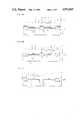
- FIG. 1Ais a diagram to explain formation of, for example, p-type polysilicon gate.
- boron ionsare implanted as indicated by arrow X with an energy of about tens of keV.
- a resist 7ais selectively opened.
- Numeral 8denotes a peripheral oxide film.
- ions of phosphor or arsenicare implanted into the polysilicon film 6.
- FIG. 1Aimplanted ions penetrate through the gate oxide film 4 and, a layer 9 is formed beneath it.
- FIG. 2is a diagram to show concentration distribution (simulation) from the boron surface when boron ions of 1 ⁇ 10 16 /cm 2 are implanted at an acceleration energy of 10 keV in the case of gate oxide film thickness of 13 nm and polysilicon film 6 thickness of 0.1 ⁇ m above it.
- the depth of junctionreaches as much as 0.3 ⁇ m as shown in FIG. 2 earlier even if implanted at the lowest energy of 10 keV in the existing ion implantation machine.
- molecule ionssuch as BF + 2 ions are used, but fluorine impurity forms defects at interface between silicon and oxide film, metal silicide film, etc.
- a plasma doping deviceAs a method which satisfies such need, a plasma doping device is known (disclose, for example, in Monthly Semiconductor World, p. 158, 1882, Vol. 2, in Japanese).
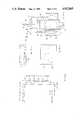
- a conventional plasma doping deviceis explained by referring to FIG. 3.
- a gas containing doping impuritiessuch as diborane (B 2 H 6 ) and arsine (AsH 3 )
- B 2 H 6diborane
- AsH 3arsine
- a metallic sample table 20 placed in the chamber 14is connected to a DC power source 22, and a silicon substrate (wafer) 2A is put in the sample table 20.
- the gas in the chamber 14is transformed into plasma by glow discharge, and the impurity ions to be doped are accelerated by the electric field in an ion sheath 26 formed around the sample table 20 and wafer 2A working as the cathodes, and are doped into the wafer 2A.
- the wafer 2Ais heated to 200° to 300° C.
- the substrateis at low temperature, such as about 200° C., a thin film of the impurities to be doped is deposited on the wafer surface, and hence the substrate is further heated by a heater 28 embedded in the sample table 20.
- Such deviceis partly applied in the silicon integrated circuit manufacturing process when doping impurities at high concentration from contact holes in order to reduce the contact resistance between the aluminum electrode and silicon diffusion layer after contact hole forming process.
- CMOS LSIwhen using both p + polycrystalline silicon and n + polycrystalline silicon as the gate material for enhancing the performance of CMOS LSI, only the regions to dope are opened by using a resist in order to keep the number of process at minimum, and p-type impurity and n-type impurity are injected into the non-dope polycrystalline silicon at a high concentration of over 10 16 /cm 2 , but in the conventional plasma doping device, since the operation exceeds the heat resistance limit (about 200° C.) of the photoresist, it was forced to use an expensive ion implantation device for a long time.
- the doping timemust be shortened extremely, for example, within 1 second.
- the material gase.g. B 2 H 6 , PH 3 , AsH 3
- base gasHe, H 2 , etc.
- this inventionalso presents a plasma doping method capable of doping impurities at high concentration in a short time while keeping the sample temperature beneath the degeneration temperature of the resist.
- the ions in plasmaare of low energy, impurities can be doped into a thin film of fractions of a micrometer in thickness, and a shallow junction can be formed on the substrate.
- the resistcan be used as the mask as mentioned above, this is a simple and inexpensive method of doping impurities locally in a shallow profile.
- FIG. 1A, FIG. 1Bare schematic sectional views showing conventional LSI fabricating processes
- FIG. 2is a diagram to show the characteristics of boron concentration distribution in Si and SiO 2 in the prior art
- FIG. 3shows the construction of the device used in the conventional LSI fabricating process
- FIG. 4 and FIG. 6show the construction of a plasma doping device to be used in the plasma doping method according to embodiments of this invention
- FIG. 5A to FIG. 5Care schematic sectional views showing the LSI fabricating processes according to the embodiment.
- FIG. 7Ais a plan view showing the state of injury on the resist when executing the embodiment, ad FIG. 7B is its sectional view;
- FIG. 8is a diagram to show the characteristics of boron concentration distribution in Si and SiO 2 in the embodiment.
- FIG. 9is an SEM picture showing the trench structure formed by the embodiment.
- FIG. 4numeral 14 is a vacuum chamber, 20 is an electrode (sample table), and 30 is a substrate.
- Numeral 16is a gas inlet
- 32is a high frequency power source of i.e. 13.56 MHz
- 34is a voltmeter for measuring cathode dorp voltage (abbreviated Vdc hereinafter).
- FIG. 5Ais a structural sectional view of the substrate 30 to be doped
- FIG. 5Bis a structural sectional view of a substrate 30A containing a CMOS transistor slightly differing in structure.
- the structure of the substrateis same as that explained in FIG. 1.
- Ydenotes ions in the plasma.
- this substratemay also contain a trench 31 (30B) as shown in FIG. 5C.
- FIG. 6is a schematic sectional view of a device used in an embodiment of this invention, in which numeral 14 is a vacuum chamber, 36 is a quartz chamber, 16 is a doping gas inlet, 18 is an exhaust port, 38 is a sample table with cooling mechanism, on which a substrate 30, 30A or 30B explained in FIG. 5 is a placed, 40 is a coil for generating a magnetic field, 42 is a microwave inlet, 44 is a cooling water into sample cooling mechanism, and 45 is a cooling water outlet.
- doping borona gas containing boron, for example, diborane B 2 H 6 is introduced into the chamber 14 through the gas inlet 16.
- the inside of the plasma generating chamber 14is made of quartz, which contributes to prevention of contamination of sample due to spattering of chamber side wall, and also to minimization of elimination of plasma and radicals on the wall surface.
- the inside of the chamber 14is kept at a degree of vacuum of 5 ⁇ 10 -3 Torr or more by controlling the opening angle of the conductance valve to the exhaust system communicating with the exhaust port 18 and the flow rate of B 2 H 6 .
- microwaves of tens to hundreds wattsare introduced from the inlet 42, and the magnetic field created by the coil 40 (max.. approx.
- the sample table 38is cooled by the circulating water cooled from 0° C. to about 30° C.
- superpurified water high in insulation or other liquid high in insulationis used, and by applying the electron cooling or a method of cooling by blowing He to the back side of substrate 30, etc., or other method, it is possible to apply a DC or RF bias to the sample table 38 and form a discharge region 47 in the space against the substrate.
- the potential energy between plasma and sample tablecan be set freely.
- Plasma dopingwas conducted by using this device.
- An example of doping boron by using, for example, n-type Si as semiconductor substrateis illustrated below.
- impurity gasB 2 H 6 is diluted with He to, for instance, 5%, and it is introduced into the chamber by 6 sccm, and by adjusting the conductance valve, the degree of vacuum is kept at, for example, 5 ⁇ 10 -4 Torr.
- Rf dischargeis effected between this plasma and substrate 30 or the like, keeping the state so that the Vdc meter 34 registers at -700V.
- the photoresistWhen exposed to plasma for 100 seconds in this state, the photoresist was free from damage, and the opening free from resist 7 was doped with boron at the surface concentration of about 10 22 cm -3 and depth of 50 nm, as being confirmed by the secondary ion mass spectroscopy (SIMS) analyzing method.
- the resist 7must be baked after coating and development processes, and at the degree of vacuum of about 1 ⁇ 10 - 3 Torr or higher, baking at 150° C. or higher is needed, and if somewhere between 5 ⁇ 10 -3 and 1 ⁇ 10 -3 , surface curing by far ultraviolet ray irradiation at wavelength of 200 to 300 nm should be needed.
- FIG. 7shows the photoresist 7 and its surface 7a when the degree of vacuum was controlled under 5 ⁇ 10 -3 Torr by closing the conductance valve. Numerous tiny holes 48 are observed, and function as resist is lost.
- both embodiments 1 and 2unless the density of plasma is sufficiently low, the temperature of the wafer surface goes up to exceed the heat resistance limit of the resist.
- the plasma densityelevates, and the energy application on the wafer surface increases, thereby causing the wafer temperature to exceed the heat resistance limit of the resist.
- FIG. 8shows the results of SIMS analysis of concentration distribution of boron from the surface when a structure with gate oxide film 13 nm and polysilicon 6 film thickness of 0.1 ⁇ m (for example, substrate structure 30 shown in FIG. 5A) is exposed to gas plasma of diborane (B 2 H 6 ), instead of ion implantation.
- the boronremained within the range of 50 nm depth from the surface in the polysilicon, not reaching up to the gate oxide film 4. Therefore, the penetration layer 9 in FIG. 1 as seen in ion implantation is never formed. As a result, the threshold voltage does not fluctuate.
- MOS transistorAfter depositing about 300 nm of tungsten silicide film (not show)) by sputtering method on this boron-doped polysilicon film 6 and forming pattern, heat treatment was conducted for 20 minutes at 900° C. in nitrogen atmosphere. Thus formed MOS transistor was good in the reproducibility of threshold voltage, and presented excellent characteristics.
- both source and drain electrodes 10after patterning gate polysilicon electrode 6 is described while referring to FIG. 5B.
- numeral 8is a peripheral oxide film for separation.
- the substrate temperaturedoes not exceed the heat resistance limit of the resits 7b, and even while cooling the substrate, thin film of impurities does not deposit on the surface, and it is possible to keep at a temperature where diffusion of impurities can be ignored (in this case, actually 200° C. or less), so that a dope layer of an extremely shallow (within 50 nm) profile is formed as shown in the SIMS profile in FIG. 8.
- This dimensionis applicable if the gate length is 0.25 ⁇ m or less.
- FIG. 9is a picture showing the mode of doping when a trench of 0.45 ⁇ m in width and 2.8 ⁇ m in depth is formed on a silicon wafer. This is a micrograph of the trench section by scanning electron microscope (SEM). The dark contrast portion around the trench is the high-concentration boron doped layer. This specimen is selectively etched for the ease of observation.
- Such trenchis mainly used in a DRAM of 4 megabits or greater, and according to the method shown in embodiment 2, impurities can be doped even into the perpendicular side wall of the trench having a high aspect ratio as show in FIG. 9.
- the resistcan be used as mask.
- this processconsists of only three steps: 1. lithography, 2. doping, and 3. removal of resist.
- the resistcannot be used because of high process temperature the process is twice as complicated: 1. deposition of heat resistance material, 2. lithography, 3. selective etching of heat resistant material, 4. removal of resist, 5. doping, and 6. selective etching of heat resistant material. Still more, the selective etching of heat resistant material in steps 3 and 6 is extremely difficult.
- the number of stepsincreases three or four times as much.
Landscapes
- Engineering & Computer Science (AREA)
- Physics & Mathematics (AREA)
- Condensed Matter Physics & Semiconductors (AREA)
- General Physics & Mathematics (AREA)
- Manufacturing & Machinery (AREA)
- Computer Hardware Design (AREA)
- Microelectronics & Electronic Packaging (AREA)
- Power Engineering (AREA)
- Plasma & Fusion (AREA)
- Drying Of Semiconductors (AREA)
- Plasma Technology (AREA)
Abstract
Description
This invention relates to plasma doping method, and more particularly to an impurity doping method by irradiating the surface of a sample with plasma to dope the impurity into the sample.
In a silicon integrated circuit manufacturing process, processes of doping acceptor impurities such as boron, and donor impurities such as arsenic and phosphor are repeatedly necessary. For this purpose, it is general to transform impurities into ions, and to implant the ions by accelerating them in a range from tens of kV to several kV, but for doping into polycrystalline silicon to be used in a gate of a MOS transistor or the like, diffusion from phosphorus glass, arsenic glass or boron glass, etc. is generally employed. This is because the ion implantation is poor in throughput and too high in cost because the doping quantity into polycrystalline silicon is extremely large. The method of using phosphorus glass requires three steps of (1) deposition of glass, (2) heat treatment, and (3) removal of glass, and, moreover, since phosphorus glass deposits on an entire surface of a silicon substrate, it is hard to dope locally in a certain region. On the other hand, as gate material of CMOS LSI, n+ polycrystalline silicon has been conventionally used, but as channel length is shortened, it comes t be necessary to use n+ polycrystalline silicon at a n-channel side and p+ polycrystalline silicon at a p-channel side from the aspect of control of channel threshold voltage.
To fabricate n-type and p-type polysilicon gates into one chip, in prior art, ion implantation technique must be used. FIG. 1A is a diagram to explain formation of, for example, p-type polysilicon gate. On apolysilicon film 6 formed on agate oxide film 4 on asilicon substrate 2, boron ions are implanted as indicated by arrow X with an energy of about tens of keV. In order to implant only into the p-type region, aresist 7a is selectively opened.Numeral 8 denotes a peripheral oxide film. In order to form an n-type polysilicon gate, ions of phosphor or arsenic are implanted into thepolysilicon film 6.
This method is effective as far as the gate oxide film is thick and the polysilicon film is also thick, but it is no longer applicable the transistor size is reduced, the gate oxide film becomes thin, and the polysilicon film also becomes thin in the trend of higher density and higher performance. That is, in FIG. 1A, implanted ions penetrate through thegate oxide film 4 and, a layer 9 is formed beneath it. FIG. 2 is a diagram to show concentration distribution (simulation) from the boron surface when boron ions of 1×10¹⁶ /cm2 are implanted at an acceleration energy of 10 keV in the case of gate oxide film thickness of 13 nm andpolysilicon film 6 thickness of 0.1 μm above it. In an ordinary ion implantation of 10 keV, in spite of the lowest energy, it is known that boron has invaded up to the silicons substrate by penetrating through thegate oxide film 4. Such penetration of boron into the silicon substrate is not acceptable because the threshold voltage of the MOS transistor is varied. Besides, as shown in FIG. 1B, generally in forming source anddrain electrode region 10, it is necessary to dope the impurities of high concentration locally respectively by dividing into the p-type region and n-type region, and it is forced to use an expensive ion implantation machine. However, in the source and drain electrodes, too, smaller depth of junction xj is required as transistor size is reduced. As described previously, especially in p-channel MOS, since boron ions of relatively light weight are used, the depth of junction reaches as much as 0.3 μm as shown in FIG. 2 earlier even if implanted at the lowest energy of 10 keV in the existing ion implantation machine. To solve this problem, molecule ions such as BF+2 ions are used, but fluorine impurity forms defects at interface between silicon and oxide film, metal silicide film, etc.
It hence gives rise to necessity of a method of doping locally and at low cost.
As a method which satisfies such need, a plasma doping device is known (disclose, for example, in Monthly Semiconductor World, p. 158, 1882, Vol. 2, in Japanese). A conventional plasma doping device is explained by referring to FIG. 3. Inside a groundedvacuum chamber 14, a gas containing doping impurities, such as diborane (B2 H6) and arsine (AsH3), is introduced through agas inlet 16, and is discharged from anexhaust port 18 by a vacuum exhaust device (not shown), so that the internal pressure is kept between one to several Torr. A metallic sample table 20 placed in thechamber 14 is connected to aDC power source 22, and a silicon substrate (wafer) 2A is put in the sample table 20. When a DC voltage of several hundred volts is applied to the sample table 20 throughDC power source 22, the gas in thechamber 14 is transformed into plasma by glow discharge, and the impurity ions to be doped are accelerated by the electric field in anion sheath 26 formed around the sample table 20 andwafer 2A working as the cathodes, and are doped into thewafer 2A. Generally, thewafer 2A is heated to 200° to 300° C. because it is directly exposed to plasma, but at the degree of vacuum in the DC or RF discharge region (10-2 Torr or less), if the substrate is at low temperature, such as about 200° C., a thin film of the impurities to be doped is deposited on the wafer surface, and hence the substrate is further heated by aheater 28 embedded in the sample table 20.
Such device is partly applied in the silicon integrated circuit manufacturing process when doping impurities at high concentration from contact holes in order to reduce the contact resistance between the aluminum electrode and silicon diffusion layer after contact hole forming process.
When doping impurities by using a material withstanding high temperature of oxide film such as a contact hole as mask, such conventional plasma doping device is effective because it is possible to dope locally at low cost, but when it was necessary to use a photoresist as mask, the wafer temperature became too high and it was not appropriate. For example, when using both p+ polycrystalline silicon and n+ polycrystalline silicon as the gate material for enhancing the performance of CMOS LSI, only the regions to dope are opened by using a resist in order to keep the number of process at minimum, and p-type impurity and n-type impurity are injected into the non-dope polycrystalline silicon at a high concentration of over 1016 /cm2, but in the conventional plasma doping device, since the operation exceeds the heat resistance limit (about 200° C.) of the photoresist, it was forced to use an expensive ion implantation device for a long time.
Incidentally, in a vacuum range of 7.5×1031 4 to 7.5×1031 1 Torr, a method of generating plasma at high density despite high degree of vacuum by applying a magnetic field in the direction along the surface of substrate is known (Japanese Laid-Open Pat. No. 6126219). In this method, however, since the closest part of the substrate is exposed to plasma of highest density, the substrate temperature is elevated in an extremely short time, instantly exceeding the heat resistance limit of the resist. Although it is possible to dope in this short time, it is hard to control the concentration of the impurity to be doped. That is, since start of discharge is often unstable, it is better to take enough time in order to achieve high reproducibility of concentration control. Besides, since the plasma density is a high concentration, if it is attempted to form a doped layer of a properly low concentration, the doping time must be shortened extremely, for example, within 1 second. As its countermeasure, it is necessary to dilute the material gas (e.g. B2 H6, PH3, AsH3) with base gas (He, H2, etc.), and dope in a sufficient time, and hence it is difficult to dope at high reproducibility and excellent concentration control, while keeping above the heat resistance limit of the resist.
In the explanation about this method, meanwhile, nothing is mentioned about the process of using the resist as the mask.
It is hence a primary object of this invention to present a plasma doping method capable of solving the above-discussed conventional problems.
It is another object of this invention to present a plasma doping method capable of solving the abovediscussed conventional problems.
It is another object of this invention to present a plasma doping method which has eliminating damages on the resist by controlling the degree of vacuum in the chamber above 5×1031 2 Torr, or more preferably 5×1031 3 Torr or more, when doping plasma. Besides, because of doping at high degree of vacuum, it is possible to cool the substrate in water, and this invention also presents a plasma doping method capable of doping impurities at high concentration in a short time while keeping the sample temperature beneath the degeneration temperature of the resist. Furthermore, since the ions in plasma are of low energy, impurities can be doped into a thin film of fractions of a micrometer in thickness, and a shallow junction can be formed on the substrate. In addition, since the resist can be used as the mask as mentioned above, this is a simple and inexpensive method of doping impurities locally in a shallow profile.
While the novel features of the invention are set forth in the appended claims, the invention, both as to organization and content, will be better understood and appreciated, along with other objects and features thereof, from the following detailed description taken in conjunction with the drawings.
FIG. 1A, FIG. 1B are schematic sectional views showing conventional LSI fabricating processes;
FIG. 2 is a diagram to show the characteristics of boron concentration distribution in Si and SiO2 in the prior art;
FIG. 3 shows the construction of the device used in the conventional LSI fabricating process;
FIG. 4 and FIG. 6 show the construction of a plasma doping device to be used in the plasma doping method according to embodiments of this invention;
FIG. 5A to FIG. 5C are schematic sectional views showing the LSI fabricating processes according to the embodiment;
FIG. 7A is a plan view showing the state of injury on the resist when executing the embodiment, ad FIG. 7B is its sectional view;
FIG. 8 is a diagram to show the characteristics of boron concentration distribution in Si and SiO2 in the embodiment; and
FIG. 9 is an SEM picture showing the trench structure formed by the embodiment.
Referring now to the drawings, a plasma doping method according to a first embodiment of this invention is explained below. In FIG. 4, numeral 14 is a vacuum chamber, 20 is an electrode (sample table), and 30 is a substrate.Numeral 16 is a gas inlet, 32 is a high frequency power source of i.e. 13.56 MHz, and 34 is a voltmeter for measuring cathode dorp voltage (abbreviated Vdc hereinafter).
FIG. 5A is a structural sectional view of thesubstrate 30 to be doped, and FIG. 5B is a structural sectional view of asubstrate 30A containing a CMOS transistor slightly differing in structure. The structure of the substrate is same as that explained in FIG. 1. In the drawing, Y denotes ions in the plasma. Incidentally, this substrate may also contain a trench 31 (30B) as shown in FIG. 5C.
Its operation is explained by referring to FIG. 4. As the impurity gas to be doped into thesubstrate 30, B2 H6 (He base 5%) was used, and injected into thevacuum chamber 14 at 10 sccm through thegas inlet 16. The inside of the vacuum chamber was kept at a degree of vacuum of 2×1031 3 Torr, and an electric power was supplied form the highfrequency power source 32 so that theVdc meter 34 indicates -700V, for 100 seconds, and doping was effected.
When a similar experiment was conducted at 2×1031 2 Torr, existence of boron in the order of 1021 cm-3 was similarly recognized, but when doped at a higher degree of vacuum of over 5×10⁻² Torr, a boron film began to be formed on the surface of thesubstrate 30, and it was found that the concentration control became difficult. In this region, too, it was confirmed that the resist 7 was degenerated. To the contrary, at 1×1031 3 Torr or less, plasma generation was difficult, and doping was impossible.
Incidentally, when doping n-type impurities, AsH3, PH3, or a similar gas may be used.
FIG. 6 is a schematic sectional view of a device used in an embodiment of this invention, in whichnumeral 14 is a vacuum chamber, 36 is a quartz chamber, 16 is a doping gas inlet, 18 is an exhaust port, 38 is a sample table with cooling mechanism, on which asubstrate chamber 14 through thegas inlet 16. The inside of theplasma generating chamber 14 is made of quartz, which contributes to prevention of contamination of sample due to spattering of chamber side wall, and also to minimization of elimination of plasma and radicals on the wall surface. The inside of thechamber 14 is kept at a degree of vacuum of 5×10⁻³ Torr or more by controlling the opening angle of the conductance valve to the exhaust system communicating with theexhaust port 18 and the flow rate of B2 H6. At frequency of 2.45 GHz, microwaves of tens to hundreds watts are introduced from the inlet 42, and the magnetic field created by the coil 40 (max.. approx. 900 Gauss) and electrons in the plasma produce a state close to an electron cyclotron resonance (ECR), and a plasma of relatively high density is produced in spite of high degree of vacuum. The sample table 38 is cooled by the circulating water cooled from 0° C. to about 30° C. For cooling the sample table 38, superpurified water high in insulation or other liquid high in insulation is used, and by applying the electron cooling or a method of cooling by blowing He to the back side ofsubstrate 30, etc., or other method, it is possible to apply a DC or RF bias to the sample table 38 and form adischarge region 47 in the space against the substrate. Thus, the potential energy between plasma and sample table can be set freely.
Plasma doping was conducted by using this device. An example of doping boron by using, for example, n-type Si as semiconductor substrate is illustrated below. As impurity gas, B2 H6 is diluted with He to, for instance, 5%, and it is introduced into the chamber by 6 sccm, and by adjusting the conductance valve, the degree of vacuum is kept at, for example, 5×10⁻⁴ Torr. By generating plasma in ECR condition, Rf discharge is effected between this plasma andsubstrate 30 or the like, keeping the state so that theVdc meter 34 registers at -700V. When exposed to plasma for 100 seconds in this state, the photoresist was free from damage, and the opening free from resist 7 was doped with boron at the surface concentration of about 1022 cm-3 and depth of 50 nm, as being confirmed by the secondary ion mass spectroscopy (SIMS) analyzing method. In this case, the resist 7 must be baked after coating and development processes, and at the degree of vacuum of about 1×10- 3 Torr or higher, baking at 150° C. or higher is needed, and if somewhere between 5×10⁻³ and 1×10⁻³, surface curing by far ultraviolet ray irradiation at wavelength of 200 to 300 nm should be needed.
FIG. 7 shows thephotoresist 7 and itssurface 7a when the degree of vacuum was controlled under 5×10⁻³ Torr by closing the conductance valve. Numeroustiny holes 48 are observed, and function as resist is lost.
Anyway, in bothembodiments
This is to explain an example of doping borons on Si substrates containing MOS structure and trench shape as explained in FIG. 5, by using the device described inembodiment 2. Thesubstrate 30 is put on the sample table 38 in FIG. 6. As shown in FIG. 5, on thissubstrate 30, after sequentially passing through the C-MOS transistor forming processes, a gate oxide film 4 (for example 13 nm) andpolysilicon film 6 for gate electrode (for example, 0.1 μm) are laminated on anactive region 50 separated from aperipheral oxide film 8, and it is selectively opened by resist 7a. In this case, because of boron doping, the p-MOS region is opened.
FIG. 8 shows the results of SIMS analysis of concentration distribution of boron from the surface when a structure with gate oxide film 13 nm andpolysilicon 6 film thickness of 0.1 μm (for example,substrate structure 30 shown in FIG. 5A) is exposed to gas plasma of diborane (B2 H6), instead of ion implantation. The boron remained within the range of 50 nm depth from the surface in the polysilicon, not reaching up to thegate oxide film 4. Therefore, the penetration layer 9 in FIG. 1 as seen in ion implantation is never formed. As a result, the threshold voltage does not fluctuate.
After depositing about 300 nm of tungsten silicide film (not show)) by sputtering method on this boron-dopedpolysilicon film 6 and forming pattern, heat treatment was conducted for 20 minutes at 900° C. in nitrogen atmosphere. Thus formed MOS transistor was good in the reproducibility of threshold voltage, and presented excellent characteristics.
Meanwhile, to realize 30B, an example of doping by plasma, without ion implantation, both source and drainelectrodes 10, after patterninggate polysilicon electrode 6 is described while referring to FIG. 5B. After patterning thegate electrode 6 by dry etching method, and pMOS region and nMOS region are selectively opened by resist 7b. In this case, to dope boron, pMOS region is opened. In this state, while cooling the sample table 38 in FIG. 6, doping is conducted in the condition same as inembodiment 2. In FIG. 5B, numeral 8 is a peripheral oxide film for separation. When doped in this condition, the substrate temperature does not exceed the heat resistance limit of theresits 7b, and even while cooling the substrate, thin film of impurities does not deposit on the surface, and it is possible to keep at a temperature where diffusion of impurities can be ignored (in this case, actually 200° C. or less), so that a dope layer of an extremely shallow (within 50 nm) profile is formed as shown in the SIMS profile in FIG. 8. This dimension is applicable if the gate length is 0.25 μm or less. Furthermore, when doping into source and drain in a separate process from doping into gate electrode, as shown in FIGS. 5A, 5B, 8, impurities will not penetrate beneath the gate even in a polysilicon film of 0.1 μm or less, and asperities may be minimized structurally, and which makes easier the process of flattening which is important in the fabrication process of LSI. FIG. 9 is a picture showing the mode of doping when a trench of 0.45 μm in width and 2.8 μm in depth is formed on a silicon wafer. This is a micrograph of the trench section by scanning electron microscope (SEM). The dark contrast portion around the trench is the high-concentration boron doped layer. This specimen is selectively etched for the ease of observation. Such trench is mainly used in a DRAM of 4 megabits or greater, and according to the method shown inembodiment 2, impurities can be doped even into the perpendicular side wall of the trench having a high aspect ratio as show in FIG. 9. At this time, needless to say, the resist can be used as mask. When using the resist, this process consists of only three steps: 1. lithography, 2. doping, and 3. removal of resist. But when the resist cannot be used because of high process temperature the process is twice as complicated: 1. deposition of heat resistance material, 2. lithography, 3. selective etching of heat resistant material, 4. removal of resist, 5. doping, and 6. selective etching of heat resistant material. Still more, the selective etching of heat resistant material insteps 3 and 6 is extremely difficult. Moreover, when a trench is contained in the substrate, the number of steps increases three or four times as much.
While specific embodiments of the invention have been illustrated and described herein, it is realized that other modifications and changes will occur to those skilled in the art. It is therefore to be understood that the appended claims are intended to cover all modifications and changes as fall within the true spirit and scope of the invention.
Claims (5)
1. A process of plasma doping a substrate comprising the steps of:
(a) providing an apparatus possessing a mechanism capable of applying microwave and magnetic field satisfying the electron cyclotron resonance condition, in a vacuum chamber;
(b) placing a substrate coated by a resist having an opening on a sample table disposed in said vacuum chamber;
(c) generating plasma by introducing a gas containing a specific element into said vacuum chamber, said plasma being generated in said vacuum chamber at a vacuum higher than 5×10⁻³ Torr;
(d) generating a discharge between said vacuum chamber and said substrate by applying high frequency or direct-current electric power to said sample table; and
(e) doping said substrate with an impurity containing said specific element in said plasma, with said resist being left over on said substrate, by making use of the potential difference produced between said substrate and said plasma, and wherein said substrate and said sample table are cooled during the plasma doping process.
2. A process of plasma doping a substrate according to claim 1, wherein a semiconductor substrate is used as the substrate to be doped.
3. A process of plasma doping substrate according to claim 2, wherein a silicon substrate is used as the substrate to be doped.
4. A process of plasma doping a substrate according to claim 1, wherein a semiconductor substrate is used as the substrate to be doped, and a substrate containing a structure composed of an insulation film formed on this semiconductor substrate and a semiconductor thin film on said insulating film is used.
5. A process of plasma doping a substrate according to claim 4, wherein silicon is used as the semiconductor substrate to be doped, a gate insulation film is formed on this silicon substrate, and the silicon substrate containing a structure having a gate electrode film deposited on said insulation film, and part of plural positions of said silicon substrate opened in the vicinity of said structure is used.
Applications Claiming Priority (8)
| Application Number | Priority Date | Filing Date | Title |
|---|---|---|---|
| JP62-132464 | 1987-05-28 | ||
| JP13246487 | 1987-05-28 | ||
| JP62-173209 | 1987-07-10 | ||
| JP17320987 | 1987-07-10 | ||
| JP62-195911 | 1987-08-05 | ||
| JP19591187 | 1987-08-05 | ||
| JP2608888 | 1988-02-05 | ||
| JP63-26088 | 1988-02-05 |
Publications (1)
| Publication Number | Publication Date |
|---|---|
| US4912065Atrue US4912065A (en) | 1990-03-27 |
Family
ID=27458429
Family Applications (1)
| Application Number | Title | Priority Date | Filing Date |
|---|---|---|---|
| US07/198,827Expired - LifetimeUS4912065A (en) | 1987-05-28 | 1988-05-26 | Plasma doping method |
Country Status (2)
| Country | Link |
|---|---|
| US (1) | US4912065A (en) |
| KR (1) | KR920004515B1 (en) |
Cited By (90)
| Publication number | Priority date | Publication date | Assignee | Title |
|---|---|---|---|---|
| US5270250A (en)* | 1991-10-08 | 1993-12-14 | M. Setek Co., Ltd. | Method of fabricating semiconductor substrate having very shallow impurity diffusion layer |
| US5425392A (en)* | 1993-05-26 | 1995-06-20 | Micron Semiconductor, Inc. | Method DRAM polycide rowline formation |
| US5532185A (en)* | 1991-03-27 | 1996-07-02 | Seiko Instruments Inc. | Impurity doping method with adsorbed diffusion source |
| EP0771020A2 (en) | 1995-10-23 | 1997-05-02 | Matsushita Electric Industrial Co., Ltd. | Impurity introduction method using a solid source of impurity, apparatus thereof and method of manufacturing a semiconductor device |
| US5716862A (en)* | 1993-05-26 | 1998-02-10 | Micron Technology, Inc. | High performance PMOSFET using split-polysilicon CMOS process incorporating advanced stacked capacitior cells for fabricating multi-megabit DRAMS |
| US5837592A (en)* | 1995-12-07 | 1998-11-17 | Taiwan Semiconductor Manufacturing Company, Ltd. | Method for stabilizing polysilicon resistors |
| US5846867A (en)* | 1995-12-20 | 1998-12-08 | Sony Corporation | Method of producing Si-Ge base heterojunction bipolar device |
| US5851906A (en)* | 1995-08-10 | 1998-12-22 | Matsushita Electric Industrial Co., Ltd. | Impurity doping method |
| US5874352A (en)* | 1989-12-06 | 1999-02-23 | Sieko Instruments Inc. | Method of producing MIS transistors having a gate electrode of matched conductivity type |
| US5976925A (en)* | 1997-12-01 | 1999-11-02 | Advanced Micro Devices | Process of fabricating a semiconductor devise having asymmetrically-doped active region and gate electrode |
| US6051482A (en)* | 1997-11-20 | 2000-04-18 | Winbond Electronics Corp. | Method for manufacturing buried-channel PMOS |
| US6087246A (en)* | 1997-04-21 | 2000-07-11 | Lg Semicon Co., Ltd. | Method for fabricating dual gate semiconductor device |
| US6237527B1 (en) | 1999-08-06 | 2001-05-29 | Axcelis Technologies, Inc. | System for improving energy purity and implant consistency, and for minimizing charge accumulation of an implanted substrate |
| US6403453B1 (en)* | 2000-07-27 | 2002-06-11 | Sharp Laboratories Of America, Inc. | Dose control technique for plasma doping in ultra-shallow junction formations |
| US6472302B1 (en) | 2001-06-12 | 2002-10-29 | Promos Technologies, Inc. | Integration method for raised contact formation for sub-150 nm devices |
| US6475906B1 (en) | 2001-07-05 | 2002-11-05 | Promos Technologies, Inc. | Gate contact etch sequence and plasma doping method for sub-150 NM DT-based DRAM devices |
| US20030047449A1 (en)* | 2000-08-11 | 2003-03-13 | Applied Materials, Inc. | Method to drive spatially separate resonant structure with spatially distinct plasma secondaries using a single generator and switching elements |
| EP1333474A3 (en)* | 1999-08-18 | 2003-10-29 | Motorola, Inc. | A method for forming a deep trench in a semiconductor substrate |
| US6642620B1 (en) | 2000-04-13 | 2003-11-04 | Micron Technology, Inc. | Integrated circuits having low resistivity contacts and the formation thereof using an in situ plasma doping and clean |
| US20030226641A1 (en)* | 2000-08-11 | 2003-12-11 | Applied Materials, Inc. | Externally excited torroidal plasma source with magnetic control of ion distribution |
| US20040107906A1 (en)* | 2000-08-11 | 2004-06-10 | Applied Materials, Inc. | Plasma immersion ion implantation apparatus including a plasma source having low dissociation and low minimum plasma voltage |
| US20040107907A1 (en)* | 2000-08-11 | 2004-06-10 | Applied Materials, Inc. | Plasma immersion ion implantation system including a plasma source having low dissociation and low minimum plasma voltage |
| US20040121570A1 (en)* | 2002-12-20 | 2004-06-24 | Chung Eun-Ae | Methods of fabricating contacts for semiconductor devices utilizing a pre-flow process and devices made thereby |
| US20040149218A1 (en)* | 2000-08-11 | 2004-08-05 | Applied Materials, Inc. | Plasma immersion ion implantation process using a capacitively coupled plasma source having low dissociation and low minimum plasma voltage |
| US20040149219A1 (en)* | 2002-10-02 | 2004-08-05 | Tomohiro Okumura | Plasma doping method and plasma doping apparatus |
| US20040165180A1 (en)* | 2003-02-20 | 2004-08-26 | David Voeller | Method and apparatus for vehicle service system with imaging components |
| US20040200417A1 (en)* | 2002-06-05 | 2004-10-14 | Applied Materials, Inc. | Very low temperature CVD process with independently variable conformality, stress and composition of the CVD layer |
| US20050051272A1 (en)* | 2000-08-11 | 2005-03-10 | Applied Materials, Inc. | Plasma immersion ion implantation process using an inductively coupled plasma source having low dissociation and low minimum plasma voltage |
| US20050070073A1 (en)* | 2000-08-11 | 2005-03-31 | Applied Materials, Inc. | Silicon-on-insulator wafer transfer method using surface activation plasma immersion ion implantation for wafer-to-wafer adhesion enhancement |
| US6893907B2 (en) | 2002-06-05 | 2005-05-17 | Applied Materials, Inc. | Fabrication of silicon-on-insulator structure using plasma immersion ion implantation |
| US20050136604A1 (en)* | 2000-08-10 | 2005-06-23 | Amir Al-Bayati | Semiconductor on insulator vertical transistor fabrication and doping process |
| US20050170669A1 (en)* | 2003-09-08 | 2005-08-04 | Tomohiro Okumura | Plasma processing method and apparatus |
| US20050191828A1 (en)* | 2000-08-11 | 2005-09-01 | Applied Materials, Inc. | Method for ion implanting insulator material to reduce dielectric constant |
| US20050191827A1 (en)* | 2000-08-11 | 2005-09-01 | Collins Kenneth S. | Plasma immersion ion implantation process |
| US20050214478A1 (en)* | 2004-03-26 | 2005-09-29 | Applied Materials, Inc. | Chemical vapor deposition plasma process using plural ion shower grids |
| US20050211546A1 (en)* | 2004-03-26 | 2005-09-29 | Applied Materials, Inc. | Reactive sputter deposition plasma process using an ion shower grid |
| US20050214477A1 (en)* | 2004-03-26 | 2005-09-29 | Applied Materials, Inc. | Chemical vapor deposition plasma process using an ion shower grid |
| US20050211171A1 (en)* | 2004-03-26 | 2005-09-29 | Applied Materials, Inc. | Chemical vapor deposition plasma reactor having an ion shower grid |
| US20050211170A1 (en)* | 2004-03-26 | 2005-09-29 | Applied Materials, Inc. | Chemical vapor deposition plasma reactor having plural ion shower grids |
| US20050230047A1 (en)* | 2000-08-11 | 2005-10-20 | Applied Materials, Inc. | Plasma immersion ion implantation apparatus |
| US20060019477A1 (en)* | 2004-07-20 | 2006-01-26 | Hiroji Hanawa | Plasma immersion ion implantation reactor having an ion shower grid |
| US20060019039A1 (en)* | 2004-07-20 | 2006-01-26 | Applied Materials, Inc. | Plasma immersion ion implantation reactor having multiple ion shower grids |
| US20060043065A1 (en)* | 2004-08-26 | 2006-03-02 | Applied Materials, Inc. | Gasless high voltage high contact force wafer contact-cooling electrostatic chuck |
| US20060081558A1 (en)* | 2000-08-11 | 2006-04-20 | Applied Materials, Inc. | Plasma immersion ion implantation process |
| US20060088655A1 (en)* | 2004-10-23 | 2006-04-27 | Applied Materials, Inc. | RF measurement feedback control and diagnostics for a plasma immersion ion implantation reactor |
| US20060121661A1 (en)* | 2004-12-08 | 2006-06-08 | Electronics And Telecommunications Research Institute | Non-volatile memory device using mobile ionic charge and method of manufacturing the same |
| US7094670B2 (en) | 2000-08-11 | 2006-08-22 | Applied Materials, Inc. | Plasma immersion ion implantation process |
| US7094316B1 (en) | 2000-08-11 | 2006-08-22 | Applied Materials, Inc. | Externally excited torroidal plasma source |
| US7109098B1 (en) | 2005-05-17 | 2006-09-19 | Applied Materials, Inc. | Semiconductor junction formation process including low temperature plasma deposition of an optical absorption layer and high speed optical annealing |
| US20060237136A1 (en)* | 2005-04-26 | 2006-10-26 | Andrew Nguyen | O-ringless tandem throttle valve for a plasma reactor chamber |
| US20060263540A1 (en)* | 2005-05-17 | 2006-11-23 | Kartik Ramaswamy | Process for low temperature plasma deposition of an optical absorption layer and high speed optical annealing |
| US20060264060A1 (en)* | 2005-05-17 | 2006-11-23 | Kartik Ramaswamy | Low temperature plasma deposition process for carbon layer deposition |
| US20060260545A1 (en)* | 2005-05-17 | 2006-11-23 | Kartik Ramaswamy | Low temperature absorption layer deposition and high speed optical annealing system |
| US20070032004A1 (en)* | 2005-08-08 | 2007-02-08 | Applied Materials, Inc. | Copper barrier reflow process employing high speed optical annealing |
| US20070032082A1 (en)* | 2005-08-08 | 2007-02-08 | Applied Materials, Inc. | Semiconductor substrate process using an optically writable carbon-containing mask |
| US20070032095A1 (en)* | 2005-08-08 | 2007-02-08 | Applied Materials, Inc. | Copper conductor annealing process employing high speed optical annealing with a low temperature-deposited optical absorber layer |
| US20070032054A1 (en)* | 2005-08-08 | 2007-02-08 | Applied Materials, Inc. | Semiconductor substrate process using a low temperature deposited carbon-containing hard mask |
| US20070037367A1 (en)* | 2002-07-11 | 2007-02-15 | Tomohiro Okumura | Apparatus for plasma doping |
| US20070042580A1 (en)* | 2000-08-10 | 2007-02-22 | Amir Al-Bayati | Ion implanted insulator material with reduced dielectric constant |
| US20070111548A1 (en)* | 2005-05-12 | 2007-05-17 | Matsushita Electric Industrial Co., Ltd. | Plasma doping method and plasma doping apparatus |
| US20070123931A1 (en)* | 1997-11-07 | 2007-05-31 | Salviac Limited | Embolic protection system |
| US20070166846A1 (en)* | 2004-12-13 | 2007-07-19 | Matsushita Electric Industrial Co., Ltd. | Plasma doping method |
| US20070264808A1 (en)* | 2006-05-11 | 2007-11-15 | Hynix Semiconductor Inc. | Plasma doping method and method for fabricating semiconductor device using the same |
| CN100373549C (en)* | 2003-07-10 | 2008-03-05 | 松下电器产业株式会社 | Plasma doping device |
| US20080166861A1 (en)* | 2005-03-30 | 2008-07-10 | Matsushita Electric Industrial Co., Ltd. | Impurity introducing apparatus and impurity introducing method |
| US20080173237A1 (en)* | 2007-01-19 | 2008-07-24 | Collins Kenneth S | Plasma Immersion Chamber |
| US20080233723A1 (en)* | 2006-10-03 | 2008-09-25 | Matsushita Electric Industrial Co., Ltd | Plasma doping method and apparatus |
| US20080258082A1 (en)* | 2004-11-02 | 2008-10-23 | Tomohiro Okumura | Plasma Processing Method and Plasma Processing Apparatus |
| US20090026540A1 (en)* | 2007-07-27 | 2009-01-29 | Matsushita Electric Industrial, Ltd. | Semiconductor device and method for producing the same |
| US20090068769A1 (en)* | 2005-04-04 | 2009-03-12 | Tomohiro Okumura | Method and Apparatus for Plasma Processing |
| US20090130335A1 (en)* | 2005-09-01 | 2009-05-21 | Tomohiro Okumura | Plasma processing apparatus, plasma processing method, dielectric window used therein, and manufacturing method of such a dielectric window |
| US20090176355A1 (en)* | 2005-03-30 | 2009-07-09 | Panasonic Corporation | Plasma Doping Method and Plasma Processing Device |
| US20090181526A1 (en)* | 2005-03-30 | 2009-07-16 | Tomohiro Okumura | Plasma Doping Method and Apparatus |
| US20090233427A1 (en)* | 2006-11-15 | 2009-09-17 | Yuichiro Sasaki | Plasma doping method |
| US20090289300A1 (en)* | 2007-07-27 | 2009-11-26 | Yuichiro Sasaki | Semiconductor device and method for producing the same |
| US20090317963A1 (en)* | 2007-08-31 | 2009-12-24 | Keiichi Nakamoto | Plasma doping processing device and method thereof |
| US20100009469A1 (en)* | 2008-03-05 | 2010-01-14 | Takayuki Kai | Plasma doping method and apparatus |
| US20100075489A1 (en)* | 2007-01-22 | 2010-03-25 | Yuichiro Sasaki | Method for producing semiconductor device and semiconductor producing apparatus |
| US20100098837A1 (en)* | 2005-02-23 | 2010-04-22 | Panasonic Corporation | Plasma doping method and apparatus |
| US20100095889A1 (en)* | 2008-08-20 | 2010-04-22 | Takayuki Kai | Plasma doping apparatus |
| US20100297836A1 (en)* | 2007-12-28 | 2010-11-25 | Panasonic Corporation | Plasma doping apparatus and method, and method for manufacturing semiconductor device |
| US20100317180A1 (en)* | 2009-06-15 | 2010-12-16 | Hynix Semiconductor Inc. | Method of Doping P-type Impurity Ions in Dual Poly Gate and Method of Forming Dual Poly Gate Using the Same |
| US20110049628A1 (en)* | 2009-02-12 | 2011-03-03 | Tomohiro Okumura | Semiconductor device, method for fabricating the same, and plasma doping system |
| US7939388B2 (en) | 2006-10-25 | 2011-05-10 | Panasonic Corporation | Plasma doping method and plasma doping apparatus |
| US20110147813A1 (en)* | 2009-12-17 | 2011-06-23 | Yuichiro Sasaki | Semiconductor device and method for fabricating the same |
| US8450819B2 (en) | 2010-11-09 | 2013-05-28 | Panasonic Corporation | Plasma doping method and apparatus thereof |
| US8574972B2 (en) | 2009-12-28 | 2013-11-05 | Panasonic Corporation | Method for fabricating semiconductor device and plasma doping apparatus |
| EP2750167A1 (en)* | 2012-12-31 | 2014-07-02 | Imec | Method for tuning the effective work function of a gate structure in a semiconductor device |
| US8889534B1 (en) | 2013-05-29 | 2014-11-18 | Tokyo Electron Limited | Solid state source introduction of dopants and additives for a plasma doping process |
| US20150123071A1 (en)* | 2011-07-22 | 2015-05-07 | Intermolecular Inc. | Method for Forming Metal Oxides and Silicides in a Memory Device |
Families Citing this family (1)
| Publication number | Priority date | Publication date | Assignee | Title |
|---|---|---|---|---|
| KR100387260B1 (en)* | 1996-06-21 | 2003-08-14 | 주식회사 하이닉스반도체 | Method for forming electrode of semiconductor device |
Citations (8)
| Publication number | Priority date | Publication date | Assignee | Title |
|---|---|---|---|---|
| US3880675A (en)* | 1971-09-18 | 1975-04-29 | Agency Ind Science Techn | Method for fabrication of lateral transistor |
| US4382099A (en)* | 1981-10-26 | 1983-05-03 | Motorola, Inc. | Dopant predeposition from high pressure plasma source |
| US4434036A (en)* | 1981-05-12 | 1984-02-28 | Siemens Aktiengesellschaft | Method and apparatus for doping semiconductor material |
| US4465529A (en)* | 1981-06-05 | 1984-08-14 | Mitsubishi Denki Kabushiki Kaisha | Method of producing semiconductor device |
| JPS6146044A (en)* | 1984-08-11 | 1986-03-06 | Fujitsu Ltd | Manufacturing method of semiconductor device |
| US4668365A (en)* | 1984-10-25 | 1987-05-26 | Applied Materials, Inc. | Apparatus and method for magnetron-enhanced plasma-assisted chemical vapor deposition |
| US4698104A (en)* | 1984-12-06 | 1987-10-06 | Xerox Corporation | Controlled isotropic doping of semiconductor materials |
| US4737379A (en)* | 1982-09-24 | 1988-04-12 | Energy Conversion Devices, Inc. | Plasma deposited coatings, and low temperature plasma method of making same |
- 1988
- 1988-05-26USUS07/198,827patent/US4912065A/ennot_activeExpired - Lifetime
- 1988-05-28KRKR1019880006315Apatent/KR920004515B1/ennot_activeExpired
Patent Citations (8)
| Publication number | Priority date | Publication date | Assignee | Title |
|---|---|---|---|---|
| US3880675A (en)* | 1971-09-18 | 1975-04-29 | Agency Ind Science Techn | Method for fabrication of lateral transistor |
| US4434036A (en)* | 1981-05-12 | 1984-02-28 | Siemens Aktiengesellschaft | Method and apparatus for doping semiconductor material |
| US4465529A (en)* | 1981-06-05 | 1984-08-14 | Mitsubishi Denki Kabushiki Kaisha | Method of producing semiconductor device |
| US4382099A (en)* | 1981-10-26 | 1983-05-03 | Motorola, Inc. | Dopant predeposition from high pressure plasma source |
| US4737379A (en)* | 1982-09-24 | 1988-04-12 | Energy Conversion Devices, Inc. | Plasma deposited coatings, and low temperature plasma method of making same |
| JPS6146044A (en)* | 1984-08-11 | 1986-03-06 | Fujitsu Ltd | Manufacturing method of semiconductor device |
| US4668365A (en)* | 1984-10-25 | 1987-05-26 | Applied Materials, Inc. | Apparatus and method for magnetron-enhanced plasma-assisted chemical vapor deposition |
| US4698104A (en)* | 1984-12-06 | 1987-10-06 | Xerox Corporation | Controlled isotropic doping of semiconductor materials |
Cited By (171)
| Publication number | Priority date | Publication date | Assignee | Title |
|---|---|---|---|---|
| US5874352A (en)* | 1989-12-06 | 1999-02-23 | Sieko Instruments Inc. | Method of producing MIS transistors having a gate electrode of matched conductivity type |
| US5532185A (en)* | 1991-03-27 | 1996-07-02 | Seiko Instruments Inc. | Impurity doping method with adsorbed diffusion source |
| US5270250A (en)* | 1991-10-08 | 1993-12-14 | M. Setek Co., Ltd. | Method of fabricating semiconductor substrate having very shallow impurity diffusion layer |
| US5425392A (en)* | 1993-05-26 | 1995-06-20 | Micron Semiconductor, Inc. | Method DRAM polycide rowline formation |
| US5716862A (en)* | 1993-05-26 | 1998-02-10 | Micron Technology, Inc. | High performance PMOSFET using split-polysilicon CMOS process incorporating advanced stacked capacitior cells for fabricating multi-megabit DRAMS |
| US5851906A (en)* | 1995-08-10 | 1998-12-22 | Matsushita Electric Industrial Co., Ltd. | Impurity doping method |
| EP0771020A2 (en) | 1995-10-23 | 1997-05-02 | Matsushita Electric Industrial Co., Ltd. | Impurity introduction method using a solid source of impurity, apparatus thereof and method of manufacturing a semiconductor device |
| US5837592A (en)* | 1995-12-07 | 1998-11-17 | Taiwan Semiconductor Manufacturing Company, Ltd. | Method for stabilizing polysilicon resistors |
| US5846867A (en)* | 1995-12-20 | 1998-12-08 | Sony Corporation | Method of producing Si-Ge base heterojunction bipolar device |
| US6087246A (en)* | 1997-04-21 | 2000-07-11 | Lg Semicon Co., Ltd. | Method for fabricating dual gate semiconductor device |
| US20070123931A1 (en)* | 1997-11-07 | 2007-05-31 | Salviac Limited | Embolic protection system |
| US6051482A (en)* | 1997-11-20 | 2000-04-18 | Winbond Electronics Corp. | Method for manufacturing buried-channel PMOS |
| US5976925A (en)* | 1997-12-01 | 1999-11-02 | Advanced Micro Devices | Process of fabricating a semiconductor devise having asymmetrically-doped active region and gate electrode |
| US6237527B1 (en) | 1999-08-06 | 2001-05-29 | Axcelis Technologies, Inc. | System for improving energy purity and implant consistency, and for minimizing charge accumulation of an implanted substrate |
| EP1333474A3 (en)* | 1999-08-18 | 2003-10-29 | Motorola, Inc. | A method for forming a deep trench in a semiconductor substrate |
| US6642620B1 (en) | 2000-04-13 | 2003-11-04 | Micron Technology, Inc. | Integrated circuits having low resistivity contacts and the formation thereof using an in situ plasma doping and clean |
| US6921708B1 (en) | 2000-04-13 | 2005-07-26 | Micron Technology, Inc. | Integrated circuits having low resistivity contacts and the formation thereof using an in situ plasma doping and clean |
| US6403453B1 (en)* | 2000-07-27 | 2002-06-11 | Sharp Laboratories Of America, Inc. | Dose control technique for plasma doping in ultra-shallow junction formations |
| US20050136604A1 (en)* | 2000-08-10 | 2005-06-23 | Amir Al-Bayati | Semiconductor on insulator vertical transistor fabrication and doping process |
| US20070042580A1 (en)* | 2000-08-10 | 2007-02-22 | Amir Al-Bayati | Ion implanted insulator material with reduced dielectric constant |
| US7294563B2 (en) | 2000-08-10 | 2007-11-13 | Applied Materials, Inc. | Semiconductor on insulator vertical transistor fabrication and doping process |
| US20050191827A1 (en)* | 2000-08-11 | 2005-09-01 | Collins Kenneth S. | Plasma immersion ion implantation process |
| US7166524B2 (en) | 2000-08-11 | 2007-01-23 | Applied Materials, Inc. | Method for ion implanting insulator material to reduce dielectric constant |
| US20040107907A1 (en)* | 2000-08-11 | 2004-06-10 | Applied Materials, Inc. | Plasma immersion ion implantation system including a plasma source having low dissociation and low minimum plasma voltage |
| US7183177B2 (en) | 2000-08-11 | 2007-02-27 | Applied Materials, Inc. | Silicon-on-insulator wafer transfer method using surface activation plasma immersion ion implantation for wafer-to-wafer adhesion enhancement |
| US7288491B2 (en) | 2000-08-11 | 2007-10-30 | Applied Materials, Inc. | Plasma immersion ion implantation process |
| US7291545B2 (en) | 2000-08-11 | 2007-11-06 | Applied Materials, Inc. | Plasma immersion ion implantation process using a capacitively couple plasma source having low dissociation and low minimum plasma voltage |
| US20040149218A1 (en)* | 2000-08-11 | 2004-08-05 | Applied Materials, Inc. | Plasma immersion ion implantation process using a capacitively coupled plasma source having low dissociation and low minimum plasma voltage |
| US20030047449A1 (en)* | 2000-08-11 | 2003-03-13 | Applied Materials, Inc. | Method to drive spatially separate resonant structure with spatially distinct plasma secondaries using a single generator and switching elements |
| US7303982B2 (en) | 2000-08-11 | 2007-12-04 | Applied Materials, Inc. | Plasma immersion ion implantation process using an inductively coupled plasma source having low dissociation and low minimum plasma voltage |
| US7320734B2 (en) | 2000-08-11 | 2008-01-22 | Applied Materials, Inc. | Plasma immersion ion implantation system including a plasma source having low dissociation and low minimum plasma voltage |
| US7137354B2 (en) | 2000-08-11 | 2006-11-21 | Applied Materials, Inc. | Plasma immersion ion implantation apparatus including a plasma source having low dissociation and low minimum plasma voltage |
| US20050051272A1 (en)* | 2000-08-11 | 2005-03-10 | Applied Materials, Inc. | Plasma immersion ion implantation process using an inductively coupled plasma source having low dissociation and low minimum plasma voltage |
| US20050070073A1 (en)* | 2000-08-11 | 2005-03-31 | Applied Materials, Inc. | Silicon-on-insulator wafer transfer method using surface activation plasma immersion ion implantation for wafer-to-wafer adhesion enhancement |
| US7430984B2 (en) | 2000-08-11 | 2008-10-07 | Applied Materials, Inc. | Method to drive spatially separate resonant structure with spatially distinct plasma secondaries using a single generator and switching elements |
| US20040107906A1 (en)* | 2000-08-11 | 2004-06-10 | Applied Materials, Inc. | Plasma immersion ion implantation apparatus including a plasma source having low dissociation and low minimum plasma voltage |
| US20030226641A1 (en)* | 2000-08-11 | 2003-12-11 | Applied Materials, Inc. | Externally excited torroidal plasma source with magnetic control of ion distribution |
| US7465478B2 (en) | 2000-08-11 | 2008-12-16 | Applied Materials, Inc. | Plasma immersion ion implantation process |
| US20050191828A1 (en)* | 2000-08-11 | 2005-09-01 | Applied Materials, Inc. | Method for ion implanting insulator material to reduce dielectric constant |
| US20070119546A1 (en)* | 2000-08-11 | 2007-05-31 | Applied Materials, Inc. | Plasma immersion ion implantation apparatus including a capacitively coupled plasma source having low dissociation and low minimum plasma voltage |
| US6939434B2 (en) | 2000-08-11 | 2005-09-06 | Applied Materials, Inc. | Externally excited torroidal plasma source with magnetic control of ion distribution |
| US7094316B1 (en) | 2000-08-11 | 2006-08-22 | Applied Materials, Inc. | Externally excited torroidal plasma source |
| US7094670B2 (en) | 2000-08-11 | 2006-08-22 | Applied Materials, Inc. | Plasma immersion ion implantation process |
| US7037813B2 (en) | 2000-08-11 | 2006-05-02 | Applied Materials, Inc. | Plasma immersion ion implantation process using a capacitively coupled plasma source having low dissociation and low minimum plasma voltage |
| US20060081558A1 (en)* | 2000-08-11 | 2006-04-20 | Applied Materials, Inc. | Plasma immersion ion implantation process |
| US20060073683A1 (en)* | 2000-08-11 | 2006-04-06 | Applied Materials, Inc. | Plasma immersion ion implantation process using a capacitively coupled plasma source having low dissociation and low minimum plasma voltage |
| US20050230047A1 (en)* | 2000-08-11 | 2005-10-20 | Applied Materials, Inc. | Plasma immersion ion implantation apparatus |
| DE10210233B4 (en)* | 2001-06-12 | 2007-03-22 | Promos Technologies, Inc. | New integration process for the formation of elevated contacts for sub-150nm devices |
| US6472302B1 (en) | 2001-06-12 | 2002-10-29 | Promos Technologies, Inc. | Integration method for raised contact formation for sub-150 nm devices |
| DE10145173C2 (en)* | 2001-07-05 | 2003-10-09 | Promos Technologies Inc | Process for forming contacts in the production of an integrated DRAM circuit |
| US6475906B1 (en) | 2001-07-05 | 2002-11-05 | Promos Technologies, Inc. | Gate contact etch sequence and plasma doping method for sub-150 NM DT-based DRAM devices |
| US20070212811A1 (en)* | 2002-06-05 | 2007-09-13 | Applied Materials, Inc. | Low temperature CVD process with selected stress of the CVD layer on CMOS devices |
| US20040107909A1 (en)* | 2002-06-05 | 2004-06-10 | Applied Materials, Inc. | Plasma immersion ion implantation process using a plasma source having low dissociation and low minimum plasma voltage |
| US7700465B2 (en) | 2002-06-05 | 2010-04-20 | Applied Materials, Inc. | Plasma immersion ion implantation process using a plasma source having low dissociation and low minimum plasma voltage |
| US7393765B2 (en) | 2002-06-05 | 2008-07-01 | Applied Materials, Inc. | Low temperature CVD process with selected stress of the CVD layer on CMOS devices |
| US20040112542A1 (en)* | 2002-06-05 | 2004-06-17 | Collins Kenneth S. | Plasma immersion ion implantation apparatus including a capacitively coupled plasma source having low dissociation and low minimum plasma voltage |
| US7223676B2 (en) | 2002-06-05 | 2007-05-29 | Applied Materials, Inc. | Very low temperature CVD process with independently variable conformality, stress and composition of the CVD layer |
| US20040107908A1 (en)* | 2002-06-05 | 2004-06-10 | Applied Materials, Inc. | Plasma immersion ion implantation apparatus including an inductively coupled plasma source having low dissociation and low minimum plasma voltage |
| US20040200417A1 (en)* | 2002-06-05 | 2004-10-14 | Applied Materials, Inc. | Very low temperature CVD process with independently variable conformality, stress and composition of the CVD layer |
| US6893907B2 (en) | 2002-06-05 | 2005-05-17 | Applied Materials, Inc. | Fabrication of silicon-on-insulator structure using plasma immersion ion implantation |
| US20050051271A1 (en)* | 2002-06-05 | 2005-03-10 | Applied Materials, Inc. | Plasma immersion ion implantation system including an inductively coupled plasma source having low dissociation and low minimum plasma voltage |
| US7575987B2 (en)* | 2002-07-11 | 2009-08-18 | Panasonic Corporation | Method of plasma doping |
| US20070037367A1 (en)* | 2002-07-11 | 2007-02-15 | Tomohiro Okumura | Apparatus for plasma doping |
| US20040149219A1 (en)* | 2002-10-02 | 2004-08-05 | Tomohiro Okumura | Plasma doping method and plasma doping apparatus |
| US20110065267A1 (en)* | 2002-10-02 | 2011-03-17 | Panasonic Corporation | Plasma Doping Method and Plasma Doping Apparatus |
| US8709926B2 (en) | 2002-10-02 | 2014-04-29 | Panasonic Corporation | Plasma doping method and plasma doping apparatus |
| US7863168B2 (en) | 2002-10-02 | 2011-01-04 | Panasonic Corporation | Plasma doping method and plasma doping apparatus |
| US20070026649A1 (en)* | 2002-10-02 | 2007-02-01 | Matsushita Electric Industrial Co., Inc. | Plasma Doping Method and Plasma Doping Apparatus |
| US6953741B2 (en)* | 2002-12-20 | 2005-10-11 | Samsung Electronics Co., Ltd | Methods of fabricating contacts for semiconductor devices utilizing a pre-flow process |
| US20040121570A1 (en)* | 2002-12-20 | 2004-06-24 | Chung Eun-Ae | Methods of fabricating contacts for semiconductor devices utilizing a pre-flow process and devices made thereby |
| US20040165180A1 (en)* | 2003-02-20 | 2004-08-26 | David Voeller | Method and apparatus for vehicle service system with imaging components |
| CN100373549C (en)* | 2003-07-10 | 2008-03-05 | 松下电器产业株式会社 | Plasma doping device |
| US8404573B2 (en) | 2003-09-08 | 2013-03-26 | Panasonic Corporation | Plasma processing method and apparatus |
| US8288259B2 (en) | 2003-09-08 | 2012-10-16 | Panasonic Corporation | Plasma processing method and apparatus |
| US20110081787A1 (en)* | 2003-09-08 | 2011-04-07 | Tomohiro Okumura | Plasma processing method and apparatus |
| US7199064B2 (en)* | 2003-09-08 | 2007-04-03 | Matsushita Electric Industrial Co., Ltd. | Plasma processing method and apparatus |
| US7858537B2 (en)* | 2003-09-08 | 2010-12-28 | Panasonic Corporation | Plasma processing method and apparatus |
| US20070020958A1 (en)* | 2003-09-08 | 2007-01-25 | Tomohiro Okumura | Plasma processing method and apparatus |
| US20050170669A1 (en)* | 2003-09-08 | 2005-08-04 | Tomohiro Okumura | Plasma processing method and apparatus |
| US20050211546A1 (en)* | 2004-03-26 | 2005-09-29 | Applied Materials, Inc. | Reactive sputter deposition plasma process using an ion shower grid |
| US7291360B2 (en) | 2004-03-26 | 2007-11-06 | Applied Materials, Inc. | Chemical vapor deposition plasma process using plural ion shower grids |
| US20050214478A1 (en)* | 2004-03-26 | 2005-09-29 | Applied Materials, Inc. | Chemical vapor deposition plasma process using plural ion shower grids |
| US20050211171A1 (en)* | 2004-03-26 | 2005-09-29 | Applied Materials, Inc. | Chemical vapor deposition plasma reactor having an ion shower grid |
| US20050214477A1 (en)* | 2004-03-26 | 2005-09-29 | Applied Materials, Inc. | Chemical vapor deposition plasma process using an ion shower grid |
| US7244474B2 (en) | 2004-03-26 | 2007-07-17 | Applied Materials, Inc. | Chemical vapor deposition plasma process using an ion shower grid |
| US20050211170A1 (en)* | 2004-03-26 | 2005-09-29 | Applied Materials, Inc. | Chemical vapor deposition plasma reactor having plural ion shower grids |
| US7695590B2 (en) | 2004-03-26 | 2010-04-13 | Applied Materials, Inc. | Chemical vapor deposition plasma reactor having plural ion shower grids |
| US20060019477A1 (en)* | 2004-07-20 | 2006-01-26 | Hiroji Hanawa | Plasma immersion ion implantation reactor having an ion shower grid |
| US7767561B2 (en) | 2004-07-20 | 2010-08-03 | Applied Materials, Inc. | Plasma immersion ion implantation reactor having an ion shower grid |
| US8058156B2 (en) | 2004-07-20 | 2011-11-15 | Applied Materials, Inc. | Plasma immersion ion implantation reactor having multiple ion shower grids |
| US20060019039A1 (en)* | 2004-07-20 | 2006-01-26 | Applied Materials, Inc. | Plasma immersion ion implantation reactor having multiple ion shower grids |
| US20060043065A1 (en)* | 2004-08-26 | 2006-03-02 | Applied Materials, Inc. | Gasless high voltage high contact force wafer contact-cooling electrostatic chuck |
| US7479456B2 (en) | 2004-08-26 | 2009-01-20 | Applied Materials, Inc. | Gasless high voltage high contact force wafer contact-cooling electrostatic chuck |
| US20060088655A1 (en)* | 2004-10-23 | 2006-04-27 | Applied Materials, Inc. | RF measurement feedback control and diagnostics for a plasma immersion ion implantation reactor |
| US7666464B2 (en) | 2004-10-23 | 2010-02-23 | Applied Materials, Inc. | RF measurement feedback control and diagnostics for a plasma immersion ion implantation reactor |
| US20080258082A1 (en)* | 2004-11-02 | 2008-10-23 | Tomohiro Okumura | Plasma Processing Method and Plasma Processing Apparatus |
| US7858155B2 (en) | 2004-11-02 | 2010-12-28 | Panasonic Corporation | Plasma processing method and plasma processing apparatus |
| US20060121661A1 (en)* | 2004-12-08 | 2006-06-08 | Electronics And Telecommunications Research Institute | Non-volatile memory device using mobile ionic charge and method of manufacturing the same |
| US7348264B2 (en) | 2004-12-13 | 2008-03-25 | Matsushita Electric Industrial Co., Ltd. | Plasma doping method |
| US20070190759A1 (en)* | 2004-12-13 | 2007-08-16 | Matsushita Electric Industrial Co., Ltd. | Plasma doping method |
| US20070166846A1 (en)* | 2004-12-13 | 2007-07-19 | Matsushita Electric Industrial Co., Ltd. | Plasma doping method |
| US7407874B2 (en) | 2004-12-13 | 2008-08-05 | Matsushita Electric Industrial Co., Ltd. | Plasma doping method |
| US20080318399A1 (en)* | 2004-12-13 | 2008-12-25 | Matsushita Electric Industrial Co., Ltd. | Plasma doping method |
| US8129202B2 (en) | 2005-02-23 | 2012-03-06 | Panasonic Corporation | Plasma doping method and apparatus |
| US20100098837A1 (en)* | 2005-02-23 | 2010-04-22 | Panasonic Corporation | Plasma doping method and apparatus |
| US8257501B2 (en) | 2005-03-30 | 2012-09-04 | Panasonic Corporation | Plasma doping device with gate shutter |
| US8652953B2 (en) | 2005-03-30 | 2014-02-18 | Panasonic Corporation | Plasma doping method with gate shutter |
| US7626184B2 (en) | 2005-03-30 | 2009-12-01 | Panasonic Corporation | Impurity introducing apparatus and impurity introducing method |
| US7622725B2 (en) | 2005-03-30 | 2009-11-24 | Panaosnic Corporation | Impurity introducing apparatus and impurity introducing method |
| US20090181526A1 (en)* | 2005-03-30 | 2009-07-16 | Tomohiro Okumura | Plasma Doping Method and Apparatus |
| US20090176355A1 (en)* | 2005-03-30 | 2009-07-09 | Panasonic Corporation | Plasma Doping Method and Plasma Processing Device |
| US20090140174A1 (en)* | 2005-03-30 | 2009-06-04 | Panasonic Corporation | Impurity Introducing Apparatus and Impurity Introducing Method |
| US20080166861A1 (en)* | 2005-03-30 | 2008-07-10 | Matsushita Electric Industrial Co., Ltd. | Impurity introducing apparatus and impurity introducing method |
| US20090068769A1 (en)* | 2005-04-04 | 2009-03-12 | Tomohiro Okumura | Method and Apparatus for Plasma Processing |
| US7601619B2 (en) | 2005-04-04 | 2009-10-13 | Panasonic Corporation | Method and apparatus for plasma processing |
| US7428915B2 (en) | 2005-04-26 | 2008-09-30 | Applied Materials, Inc. | O-ringless tandem throttle valve for a plasma reactor chamber |
| US20060237136A1 (en)* | 2005-04-26 | 2006-10-26 | Andrew Nguyen | O-ringless tandem throttle valve for a plasma reactor chamber |
| US20080067439A1 (en)* | 2005-05-12 | 2008-03-20 | Matsushita Electric Industrial Co., Ltd. | Plasma doping method and plasma doping apparatus |
| US20070111548A1 (en)* | 2005-05-12 | 2007-05-17 | Matsushita Electric Industrial Co., Ltd. | Plasma doping method and plasma doping apparatus |
| US7358511B2 (en) | 2005-05-12 | 2008-04-15 | Matsushita Electric Industrial Co., Ltd. | Plasma doping method and plasma doping apparatus |
| US20070176124A1 (en)* | 2005-05-12 | 2007-08-02 | Matsushita Electric Industrial Co., Ltd. | Plasma doping method and plasma doping apparatus |
| US20060263540A1 (en)* | 2005-05-17 | 2006-11-23 | Kartik Ramaswamy | Process for low temperature plasma deposition of an optical absorption layer and high speed optical annealing |
| US7109098B1 (en) | 2005-05-17 | 2006-09-19 | Applied Materials, Inc. | Semiconductor junction formation process including low temperature plasma deposition of an optical absorption layer and high speed optical annealing |
| US7422775B2 (en) | 2005-05-17 | 2008-09-09 | Applied Materials, Inc. | Process for low temperature plasma deposition of an optical absorption layer and high speed optical annealing |
| US20060260545A1 (en)* | 2005-05-17 | 2006-11-23 | Kartik Ramaswamy | Low temperature absorption layer deposition and high speed optical annealing system |
| US20060264060A1 (en)* | 2005-05-17 | 2006-11-23 | Kartik Ramaswamy | Low temperature plasma deposition process for carbon layer deposition |
| US7312162B2 (en) | 2005-05-17 | 2007-12-25 | Applied Materials, Inc. | Low temperature plasma deposition process for carbon layer deposition |
| US20070032004A1 (en)* | 2005-08-08 | 2007-02-08 | Applied Materials, Inc. | Copper barrier reflow process employing high speed optical annealing |
| US20070032082A1 (en)* | 2005-08-08 | 2007-02-08 | Applied Materials, Inc. | Semiconductor substrate process using an optically writable carbon-containing mask |
| US7335611B2 (en) | 2005-08-08 | 2008-02-26 | Applied Materials, Inc. | Copper conductor annealing process employing high speed optical annealing with a low temperature-deposited optical absorber layer |
| US7312148B2 (en) | 2005-08-08 | 2007-12-25 | Applied Materials, Inc. | Copper barrier reflow process employing high speed optical annealing |
| US7323401B2 (en) | 2005-08-08 | 2008-01-29 | Applied Materials, Inc. | Semiconductor substrate process using a low temperature deposited carbon-containing hard mask |
| US7429532B2 (en) | 2005-08-08 | 2008-09-30 | Applied Materials, Inc. | Semiconductor substrate process using an optically writable carbon-containing mask |
| US20070032054A1 (en)* | 2005-08-08 | 2007-02-08 | Applied Materials, Inc. | Semiconductor substrate process using a low temperature deposited carbon-containing hard mask |
| US20070032095A1 (en)* | 2005-08-08 | 2007-02-08 | Applied Materials, Inc. | Copper conductor annealing process employing high speed optical annealing with a low temperature-deposited optical absorber layer |
| CN101258786B (en)* | 2005-09-01 | 2012-08-29 | 松下电器产业株式会社 | plasma processing equipment |
| US20090130335A1 (en)* | 2005-09-01 | 2009-05-21 | Tomohiro Okumura | Plasma processing apparatus, plasma processing method, dielectric window used therein, and manufacturing method of such a dielectric window |
| US20070264808A1 (en)* | 2006-05-11 | 2007-11-15 | Hynix Semiconductor Inc. | Plasma doping method and method for fabricating semiconductor device using the same |
| US7888245B2 (en) | 2006-05-11 | 2011-02-15 | Hynix Semiconductor Inc. | Plasma doping method and method for fabricating semiconductor device using the same |
| US20110217830A1 (en)* | 2006-10-03 | 2011-09-08 | Panasonic Corporation | Plasma doping method and apparatus |
| US20080233723A1 (en)* | 2006-10-03 | 2008-09-25 | Matsushita Electric Industrial Co., Ltd | Plasma doping method and apparatus |
| US7939388B2 (en) | 2006-10-25 | 2011-05-10 | Panasonic Corporation | Plasma doping method and plasma doping apparatus |
| US7790586B2 (en) | 2006-11-15 | 2010-09-07 | Panasonic Corporation | Plasma doping method |
| US20090233427A1 (en)* | 2006-11-15 | 2009-09-17 | Yuichiro Sasaki | Plasma doping method |
| US20080173237A1 (en)* | 2007-01-19 | 2008-07-24 | Collins Kenneth S | Plasma Immersion Chamber |
| US20100075489A1 (en)* | 2007-01-22 | 2010-03-25 | Yuichiro Sasaki | Method for producing semiconductor device and semiconductor producing apparatus |
| US7754503B2 (en) | 2007-01-22 | 2010-07-13 | Panasonic Corporation | Method for producing semiconductor device and semiconductor producing apparatus |
| US8063437B2 (en) | 2007-07-27 | 2011-11-22 | Panasonic Corporation | Semiconductor device and method for producing the same |
| US20090026540A1 (en)* | 2007-07-27 | 2009-01-29 | Matsushita Electric Industrial, Ltd. | Semiconductor device and method for producing the same |
| US8536000B2 (en) | 2007-07-27 | 2013-09-17 | Panasonic Corporation | Method for producing a semiconductor device have fin-shaped semiconductor regions |
| US20090289300A1 (en)* | 2007-07-27 | 2009-11-26 | Yuichiro Sasaki | Semiconductor device and method for producing the same |
| US8004045B2 (en) | 2007-07-27 | 2011-08-23 | Panasonic Corporation | Semiconductor device and method for producing the same |
| US20090317963A1 (en)* | 2007-08-31 | 2009-12-24 | Keiichi Nakamoto | Plasma doping processing device and method thereof |
| US7820230B2 (en) | 2007-08-31 | 2010-10-26 | Panasonic Corporation | Plasma doping processing device and method thereof |
| US20100297836A1 (en)* | 2007-12-28 | 2010-11-25 | Panasonic Corporation | Plasma doping apparatus and method, and method for manufacturing semiconductor device |
| US7972945B2 (en) | 2007-12-28 | 2011-07-05 | Panasonic Corporation | Plasma doping apparatus and method, and method for manufacturing semiconductor device |
| US20100009469A1 (en)* | 2008-03-05 | 2010-01-14 | Takayuki Kai | Plasma doping method and apparatus |
| US20100095889A1 (en)* | 2008-08-20 | 2010-04-22 | Takayuki Kai | Plasma doping apparatus |
| US20110049628A1 (en)* | 2009-02-12 | 2011-03-03 | Tomohiro Okumura | Semiconductor device, method for fabricating the same, and plasma doping system |
| US8324685B2 (en) | 2009-02-12 | 2012-12-04 | Panasonic Corporation | Semiconductor device having a fin-type semiconductor region |
| US20100317180A1 (en)* | 2009-06-15 | 2010-12-16 | Hynix Semiconductor Inc. | Method of Doping P-type Impurity Ions in Dual Poly Gate and Method of Forming Dual Poly Gate Using the Same |
| US8003501B2 (en)* | 2009-06-15 | 2011-08-23 | Hynix Semiconductor Inc. | Method of doping P-type impurity ions in dual poly gate and method of forming dual poly gate using the same |
| US20110147813A1 (en)* | 2009-12-17 | 2011-06-23 | Yuichiro Sasaki | Semiconductor device and method for fabricating the same |
| US8409939B2 (en) | 2009-12-17 | 2013-04-02 | Panasonic Corporation | Semiconductor device and method for fabricating the same |
| US8574972B2 (en) | 2009-12-28 | 2013-11-05 | Panasonic Corporation | Method for fabricating semiconductor device and plasma doping apparatus |
| US8450819B2 (en) | 2010-11-09 | 2013-05-28 | Panasonic Corporation | Plasma doping method and apparatus thereof |
| US20150123071A1 (en)* | 2011-07-22 | 2015-05-07 | Intermolecular Inc. | Method for Forming Metal Oxides and Silicides in a Memory Device |
| US9343673B2 (en)* | 2011-07-22 | 2016-05-17 | Intermolecular, Inc. | Method for forming metal oxides and silicides in a memory device |
| EP2750167A1 (en)* | 2012-12-31 | 2014-07-02 | Imec | Method for tuning the effective work function of a gate structure in a semiconductor device |
| US8889534B1 (en) | 2013-05-29 | 2014-11-18 | Tokyo Electron Limited | Solid state source introduction of dopants and additives for a plasma doping process |
| WO2014197145A1 (en)* | 2013-05-29 | 2014-12-11 | Tokyo Electron Limited | Solid state introduction of dopants for plasma doping |
Also Published As
| Publication number | Publication date |
|---|---|
| KR880014650A (en) | 1988-12-24 |
| KR920004515B1 (en) | 1992-06-08 |
Similar Documents
| Publication | Publication Date | Title |
|---|---|---|
| US4912065A (en) | Plasma doping method | |
| US4776925A (en) | Method of forming dielectric thin films on silicon by low energy ion beam bombardment | |
| US6335534B1 (en) | Ion implantation apparatus, ion generating apparatus and semiconductor manufacturing method with ion implantation processes | |
| US5789312A (en) | Method of fabricating mid-gap metal gates compatible with ultra-thin dielectrics | |
| US7018880B2 (en) | Method for manufacturing a MOS transistor having reduced 1/f noise | |
| US5583067A (en) | Inverse T-gate semiconductor device with self-aligned punchthrough stops and method of fabrication | |
| US5719068A (en) | Method for anisotropic etching conductive film | |
| US6017784A (en) | Manufacture method of semiconductor device with suppressed impurity diffusion from gate electrode | |
| EP0083785B1 (en) | Method of forming self-aligned field effect transistors in integrated circuit structures | |
| US6831021B2 (en) | Plasma method and apparatus for processing a substrate | |
| US5969398A (en) | Method for producing a semiconductor device and a semiconductor device | |
| US5661043A (en) | Forming a buried insulator layer using plasma source ion implantation | |
| US6081010A (en) | MOS semiconductor device with self-aligned punchthrough stops and method of fabrication | |
| US5141885A (en) | Method of fabrication of thin film transistors | |
| JPH0758695B2 (en) | Plasma doping method | |
| KR970004484B1 (en) | LDD MOSFET manufacturing method of semiconductor device | |
| US7598146B2 (en) | Self-aligned gate and method | |
| US5319231A (en) | Insulated gate semiconductor device having an elevated plateau like portion | |
| US6780700B2 (en) | Method of fabricating deep sub-micron CMOS source/drain with MDD and selective CVD silicide | |
| KR100499755B1 (en) | Method of fabricating deep sub-micron cmos source/drain with mdd and selective cvd silicide | |
| GB2074374A (en) | Method of making field effect transistors | |
| US5527719A (en) | Process for making a semiconductor MOS transistor using a fluid material | |
| US20030166328A1 (en) | Method of manufacturing semiconductor devices by sputter-doping | |
| US20010037939A1 (en) | Impurity introducing apparatus and method | |
| US5965932A (en) | Contamination free source for shallow low energy junction implants using implanted molecules containing titanium and boron |
Legal Events
| Date | Code | Title | Description |
|---|---|---|---|
| AS | Assignment | Owner name:MATSUSHITA ELECTRIC INDUSTRIAL CO., LTD., 1006 OAZ Free format text:ASSIGNMENT OF ASSIGNORS INTEREST.;ASSIGNORS:MIZUNO, BUNJI;KUBOTA, MASAFUMI;NAKAYAMA, ICHIRO;AND OTHERS;REEL/FRAME:004892/0272 Effective date:19880519 Owner name:MATSUSHITA ELECTRIC INDUSTRIAL CO., LTD., JAPAN Free format text:ASSIGNMENT OF ASSIGNORS INTEREST;ASSIGNORS:MIZUNO, BUNJI;KUBOTA, MASAFUMI;NAKAYAMA, ICHIRO;AND OTHERS;REEL/FRAME:004892/0272 Effective date:19880519 | |
| STCF | Information on status: patent grant | Free format text:PATENTED CASE | |
| FEPP | Fee payment procedure | Free format text:PAYOR NUMBER ASSIGNED (ORIGINAL EVENT CODE: ASPN); ENTITY STATUS OF PATENT OWNER: LARGE ENTITY | |
| FPAY | Fee payment | Year of fee payment:4 | |
| FPAY | Fee payment | Year of fee payment:8 | |
| FPAY | Fee payment | Year of fee payment:12 |