US4910160A - High voltage complementary NPN/PNP process - Google Patents
High voltage complementary NPN/PNP processDownload PDFInfo
- Publication number
- US4910160A US4910160AUS07/361,171US36117189AUS4910160AUS 4910160 AUS4910160 AUS 4910160AUS 36117189 AUS36117189 AUS 36117189AUS 4910160 AUS4910160 AUS 4910160A
- Authority
- US
- United States
- Prior art keywords
- dopant
- oxide
- wafer
- pnp
- npn
- Prior art date
- Legal status (The legal status is an assumption and is not a legal conclusion. Google has not performed a legal analysis and makes no representation as to the accuracy of the status listed.)
- Expired - Lifetime
Links
- 238000000034methodMethods0.000titleclaimsabstractdescription36
- 230000000295complement effectEffects0.000titledescription4
- 239000007943implantSubstances0.000claimsabstractdescription6
- 239000002019doping agentSubstances0.000claimsdescription45
- 238000009792diffusion processMethods0.000claimsdescription27
- XUIMIQQOPSSXEZ-UHFFFAOYSA-NSiliconChemical compound[Si]XUIMIQQOPSSXEZ-UHFFFAOYSA-N0.000claimsdescription26
- 229910052710siliconInorganic materials0.000claimsdescription26
- 239000010703siliconSubstances0.000claimsdescription26
- 239000000758substrateSubstances0.000claimsdescription24
- 239000012535impuritySubstances0.000claimsdescription20
- 238000002955isolationMethods0.000claimsdescription16
- 230000000873masking effectEffects0.000claimsdescription13
- ZOXJGFHDIHLPTG-UHFFFAOYSA-NBoronChemical compound[B]ZOXJGFHDIHLPTG-UHFFFAOYSA-N0.000claimsdescription12
- 229910052782aluminiumInorganic materials0.000claimsdescription12
- XAGFODPZIPBFFR-UHFFFAOYSA-NaluminiumChemical compound[Al]XAGFODPZIPBFFR-UHFFFAOYSA-N0.000claimsdescription12
- 229910052796boronInorganic materials0.000claimsdescription12
- 229910052751metalInorganic materials0.000claimsdescription9
- 239000002184metalSubstances0.000claimsdescription9
- BHEPBYXIRTUNPN-UHFFFAOYSA-Nhydridophosphorus(.) (triplet)Chemical compound[PH]BHEPBYXIRTUNPN-UHFFFAOYSA-N0.000claimsdescription8
- 229910052787antimonyInorganic materials0.000claimsdescription6
- WATWJIUSRGPENY-UHFFFAOYSA-Nantimony atomChemical compound[Sb]WATWJIUSRGPENY-UHFFFAOYSA-N0.000claimsdescription6
- 229910052581Si3N4Inorganic materials0.000claimsdescription3
- 229910052785arsenicInorganic materials0.000claimsdescription3
- RQNWIZPPADIBDY-UHFFFAOYSA-Narsenic atomChemical compound[As]RQNWIZPPADIBDY-UHFFFAOYSA-N0.000claimsdescription3
- 230000008021depositionEffects0.000claimsdescription3
- 238000005468ion implantationMethods0.000claimsdescription3
- HQVNEWCFYHHQES-UHFFFAOYSA-Nsilicon nitrideChemical compoundN12[Si]34N5[Si]62N3[Si]51N64HQVNEWCFYHHQES-UHFFFAOYSA-N0.000claimsdescription3
- 238000005530etchingMethods0.000claims5
- 230000015572biosynthetic processEffects0.000claims4
- XLYOFNOQVPJJNP-UHFFFAOYSA-NwaterSubstancesOXLYOFNOQVPJJNP-UHFFFAOYSA-N0.000claims2
- 238000012360testing methodMethods0.000abstractdescription3
- 239000010410layerSubstances0.000description44
- 238000004519manufacturing processMethods0.000description10
- 239000005360phosphosilicate glassSubstances0.000description6
- 238000000407epitaxyMethods0.000description5
- 230000035515penetrationEffects0.000description5
- 239000012298atmosphereSubstances0.000description4
- 238000005247getteringMethods0.000description4
- 150000004767nitridesChemical class0.000description4
- 239000000463materialSubstances0.000description3
- 230000003647oxidationEffects0.000description3
- 238000007254oxidation reactionMethods0.000description3
- 230000001590oxidative effectEffects0.000description3
- 229920002120photoresistant polymerPolymers0.000description3
- 238000010276constructionMethods0.000description2
- 238000000151depositionMethods0.000description2
- 230000000694effectsEffects0.000description2
- 239000012634fragmentSubstances0.000description2
- 230000007774longtermEffects0.000description2
- 238000001465metallisationMethods0.000description2
- 238000002161passivationMethods0.000description2
- XHXFXVLFKHQFAL-UHFFFAOYSA-Nphosphoryl trichlorideChemical compoundClP(Cl)(Cl)=OXHXFXVLFKHQFAL-UHFFFAOYSA-N0.000description2
- 229910052582BNInorganic materials0.000description1
- PZNSFCLAULLKQX-UHFFFAOYSA-NBoron nitrideChemical compoundN#BPZNSFCLAULLKQX-UHFFFAOYSA-N0.000description1
- OAICVXFJPJFONN-UHFFFAOYSA-NPhosphorusChemical compound[P]OAICVXFJPJFONN-UHFFFAOYSA-N0.000description1
- 239000003990capacitorSubstances0.000description1
- 230000001351cycling effectEffects0.000description1
- MROCJMGDEKINLD-UHFFFAOYSA-NdichlorosilaneChemical compoundCl[SiH2]ClMROCJMGDEKINLD-UHFFFAOYSA-N0.000description1
- 239000011521glassSubstances0.000description1
- 238000010438heat treatmentMethods0.000description1
- 239000012212insulatorSubstances0.000description1
- 230000008018meltingEffects0.000description1
- 238000002844meltingMethods0.000description1
- 239000000203mixtureSubstances0.000description1
- 229910021421monocrystalline siliconInorganic materials0.000description1
- 239000012299nitrogen atmosphereSubstances0.000description1
- 230000002093peripheral effectEffects0.000description1
- 229910052698phosphorusInorganic materials0.000description1
- 239000011574phosphorusSubstances0.000description1
- 238000004886process controlMethods0.000description1
- 239000004065semiconductorSubstances0.000description1
- 239000007858starting materialSubstances0.000description1
- 239000002344surface layerSubstances0.000description1
- FAQYAMRNWDIXMY-UHFFFAOYSA-NtrichloroboraneChemical compoundClB(Cl)ClFAQYAMRNWDIXMY-UHFFFAOYSA-N0.000description1
- 238000001947vapour-phase growthMethods0.000description1
Images


Classifications
- H—ELECTRICITY
- H10—SEMICONDUCTOR DEVICES; ELECTRIC SOLID-STATE DEVICES NOT OTHERWISE PROVIDED FOR
- H10D—INORGANIC ELECTRIC SEMICONDUCTOR DEVICES
- H10D84/00—Integrated devices formed in or on semiconductor substrates that comprise only semiconducting layers, e.g. on Si wafers or on GaAs-on-Si wafers
- H10D84/60—Integrated devices formed in or on semiconductor substrates that comprise only semiconducting layers, e.g. on Si wafers or on GaAs-on-Si wafers characterised by the integration of at least one component covered by groups H10D10/00 or H10D18/00, e.g. integration of BJTs
- H10D84/67—Complementary BJTs
- H10D84/673—Vertical complementary BJTs
- H—ELECTRICITY
- H01—ELECTRIC ELEMENTS
- H01L—SEMICONDUCTOR DEVICES NOT COVERED BY CLASS H10
- H01L21/00—Processes or apparatus adapted for the manufacture or treatment of semiconductor or solid state devices or of parts thereof
- H01L21/70—Manufacture or treatment of devices consisting of a plurality of solid state components formed in or on a common substrate or of parts thereof; Manufacture of integrated circuit devices or of parts thereof
- H01L21/71—Manufacture of specific parts of devices defined in group H01L21/70
- H01L21/76—Making of isolation regions between components
- H01L21/761—PN junctions
- H—ELECTRICITY
- H10—SEMICONDUCTOR DEVICES; ELECTRIC SOLID-STATE DEVICES NOT OTHERWISE PROVIDED FOR
- H10D—INORGANIC ELECTRIC SEMICONDUCTOR DEVICES
- H10D84/00—Integrated devices formed in or on semiconductor substrates that comprise only semiconducting layers, e.g. on Si wafers or on GaAs-on-Si wafers
- H10D84/01—Manufacture or treatment
- H10D84/0112—Integrating together multiple components covered by H10D8/00, H10D10/00 or H10D18/00, e.g. integrating multiple BJTs
- H10D84/0119—Integrating together multiple components covered by H10D8/00, H10D10/00 or H10D18/00, e.g. integrating multiple BJTs the components including complementary BJTs
- H10D84/0121—Integrating together multiple components covered by H10D8/00, H10D10/00 or H10D18/00, e.g. integrating multiple BJTs the components including complementary BJTs the complementary BJTs being vertical BJTs
- H—ELECTRICITY
- H10—SEMICONDUCTOR DEVICES; ELECTRIC SOLID-STATE DEVICES NOT OTHERWISE PROVIDED FOR
- H10D—INORGANIC ELECTRIC SEMICONDUCTOR DEVICES
- H10D84/00—Integrated devices formed in or on semiconductor substrates that comprise only semiconducting layers, e.g. on Si wafers or on GaAs-on-Si wafers
- H10D84/01—Manufacture or treatment
- H10D84/02—Manufacture or treatment characterised by using material-based technologies
- H10D84/03—Manufacture or treatment characterised by using material-based technologies using Group IV technology, e.g. silicon technology or silicon-carbide [SiC] technology
- H10D84/038—Manufacture or treatment characterised by using material-based technologies using Group IV technology, e.g. silicon technology or silicon-carbide [SiC] technology using silicon technology, e.g. SiGe
Definitions
- Patent application 853,530was filed Apr. 18, 1986, by J. Barry Small and Matthew S. Buynoski U.S. Pat. No. 4,733,650. It is titled A HIGH VOLTAGE COMPLEMENTARY NPN/PNP PROCESS. It relates to the fabrication of high performance PNP and NPN transistors in planar, monolithic, PN-junction-isolated, silicon integrated circuit (IC) structures. Previously, the PNP transistors were typically lateral structures or substrate dedicated collector devices. In either case, the high frequency performance of the PNP transistor was much worse than the NPN and, in the substrate-dedicated device, only emitter-follower circuits could be employed. The process disclosed in the application produced complementary devices having excellent high frequency performance and could be incorporated directly into conventional IC processing. The teaching in this application, which is assigned to the assignee of the present application, is incorporated herein by reference.
- the PNP power transistor devicesare fabricated using a P+ collector buried layer that is created in the IC structure by applying P type impurities or dopants to the substrate wafer prior to epitaxy. At the same time the P+ collector buried layer is created it is isolated from the substrate by the establishing of a surrounding N type well region. These same P type impurities are deposited in the isolation wall regions in the substrate wafer.
- the conventional N++ type buried layeris created in the substrate wafer in the region where NPN power transistors are to be created.
- an N+ contact regionis applied to the substrate wafer at the end of the buried layer that shall be under the collector N+ contact area. Then the epitaxial layer is grown conventionally.
- the lightly doped PNP collectoremploys aluminum as the active species which can be applied after epitaxy in a relatively short diffusion cycle because of its high diffusion rate.
- the structuremakes use of conventional boron up-diffusion and down-diffusion of the isolation and for contact to the periphery of the P+ collector buried layer. This permits the establishing of an isolated PNP power transistor of vertical construction.
- the P+ buried layer and its diffused contactwill serve to reduce PNP power transistor collector resistance.
- the NPN power transistoris fabricated above a conventional high conductivity buried layer.
- a phosphorous diffused contact dopantis applied to the edge of the buried layer.
- a similar top surface dopantis applied in registry with the lower one. After diffusion these two dopants will blend together thereby providing a low resistance sinker contact for the NPN power transistor collector.
- an N type base impurity region of the PNPis located within the confines of the P well and the NPN power transistor P type base region is applied. Then a heavy concentration of P type impurities is formed to create the PNP power transistor emitter within the confines of the N type base.
- P type impuritiesare introduced around the periphery of the P well and as a cap over the isolation region.
- the heavily doped NPN power transistor emitteris created within the confines of the P type base.
- the NPN collector contactis capped.
- the PNP isolation and contact dopingis overcoated with heavily doped P type material and the NPN collector contact is overcoated with heavily doped N type material.
- the processincludes testing of the wafer at critical stages to determine the effectiveness of the previous steps.
- the processalso includes the use of phosphosilicate glass (PSG) gettering and field threshold adjustment (FTA) along with nitride and oxide over metal for NITRIDE PLUSTM performance.
- PSGphosphosilicate glass
- FTAfield threshold adjustment
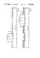
- FIGS. 1-12represent cross sections of a fragment of a silicon wafer at various stages of processing in accordance with the invention.
- the drawingis idealized and the vertical dimensions are exaggerated to show the various layers more clearly.
- ion implantationis used extensively for control of silicon dopant or impurity concentration.
- a form of shorthandis employed to characterize the ion implant.
- 1.2E13 @ 80 KeVdescribes an implant of 1.2 ⁇ 10 13 atoms per square centimeter with an energy of 80 kilo electron volts. The energy will determine the initial dopant penetration into the silicon substrate. The actual penetration will be a function of the size of the impurity ion as well as its energy. For example, the larger the ion the shallower its penetration at a given energy.
- FIG. 1A fragment of an IC wafer being processed is shown in various steps in the preferred fabrication process. It is to be understood that the substrate steps that result from localized oxidation are not shown. For example, if a localized impurity diffusion is performed in an oxidizing atmosphere, an oxide will be grown at the site. Typically, when an oxide is grown to a particular thickness about half of that thickness of silicon will be consumed from the substrate. This creates a surface step, but the step is typically so small that it has little effect on the device topology. The process is still essentially planar. For example, if a 4K ⁇ oxide is grown in a localized region, it will create a 2K ⁇ depression of the silicon in that region. No attempt will be made to illustrate such steps.
- the starting materialis a silicon wafer 10 having a P type impurity or dopant content of about 5 ⁇ 10 15 atoms per CC.
- An oxide 11is grown on the surface at about 1000° C. for three hours. This oxide will be about 8K ⁇ thick.
- P type substrate 10 with its oxide layer 11is provided with a photolithographically created hole or opening 13 therein. This opening defines the region where an NPN power transistor is to be incorporated into the IC.
- antimonyis implanted 2E15 @ 80 KeV.
- an antimony doped surface region 14is created.
- a new resist layer 15is applied as shown in FIG. 2 and processed to create hole 16 therein.
- Oxide layer 11is then etched to expose the surface of wafer 10 inside the hole.
- Phosphorousis then implanted at about 1.2E13 @ 100 KeV to create N type doped surface region 17. This region will ultimately form an N well that isolates the PNP power transistor to be incorporated into the IC.
- the resistis carefully cleaned from the wafer surface and the wafer subjected to a diffusion cycle that involves heating the wafer in an oxidizing atmosphere to about 1270° C. for 8 hours.
- a diffusion cyclethat involves heating the wafer in an oxidizing atmosphere to about 1270° C. for 8 hours.
- the antimony at region 14 and the phosphorous at region 17will diffuse into the substrate 10 as shown in FIG. 3.
- Region 14will produce an N++ region 19 and region 17 will produce N region 20.
- antimonyis a much slower diffuser than phosphorous its penetration into the substrate 10 will be substantially less.
- a 4K ⁇ oxide 18 and 18'will be grown over region 19 and 20. This diffusion temperature is the highest in the entire fabrication process so that the substrate impurity penetration shown in FIG. 3 is not altered substantially in subsequent steps.
- a new photoresist layer 22is applied to the wafer and holes therein are created at 23, 24, 25 and 26.
- Hole 23is in registry with and lies inside region 20. It will ultimately define the collector of the PNP power transistor.
- Holes 24-26represent areas where PN junction isolation regions will be fabricated.
- Oxide layer 11(including its thinned region 18') will be etched through the mask holes to expose the surface of silicon substrate 10. Then, boron is implanted, about 1E15 @ 160 Kev, to create heavily doped regions 27-30.
- Resist 22is then removed from the wafer and a new resist layer 32 applied as shown in FIG. 5. It is provided with a hole 31 that, after oxide 18 is etched, exposes one end of N++ region 19. Then phosphorous is ion implanted 1E15 @ 160 KeV. This creates a heavily doped region 72.
- the waferis then coated with an epitaxially deposited layer of silicon as shown at 33 in FIG. 6.
- a conventional vapor phase deposition processusing dichlorosilane, is employed to deposit the single crystal silicon.
- the deposition cycleis operated to produce a layer about 14.5 microns thick and is doped N type to a conductivity of 2.5 ohm centimeters.
- the conductivity of the epitaxial materialis selected to optimize the NPN power transistor collectors.
- the waferis oxidized at 1000° C. for 3 hours to produce an 8k ⁇ oxide 34.
- the impurities deposited previously into substrate 10will diffuse upwardly into epitaxial layer 10 as shown in FIG. 6. However, they will only partially penetrate the epitaxial layer. Regions 19 and 20, which were subjected to higher temperature previously, will not diffuse appreciably further into substrate 10, but they will supply impurities that diffuse upwardly into epitaxial layer 33.
- region 27 of FIG. 5will produce P+ region 35 which will define the PNP power transistor collector and act as a conductive buried layer.
- N++ region 19will diffuse only slightly upwardly into the epitaxial layer to provide the NPN transistor buried layer.
- Doped region 33 of FIG. 5will produce N+ region 36 which extends upwardly from region 19. Region 28 of FIG. 5 will diffuse up to form isolation region 37. Region 29 of FIG. 5 will diffuse up to form isolation region 38 and region 30 of FIG. 5 will diffuse up to form isolation region 39. Since regions 37-39 are P+ type their extensions into P type substrate 10 are ohmic and are therefore shown dashed.
- a photoresist mask(not shown) is applied to the wafer and provided with an opening 40 that is in registry with region 36.
- This maskis employed to photolithographically open a hole in the oxide 34 at 40, as shown in FIG. 7.
- the waferis subjected to a conventional phosphorus diffusion predep that is operated to produce an N+ region 41 of about one to two ohms per square.
- the waferis subjected to oxidation at 950° C. which diffuses the phosphorous to create an N+ type region shown as element 42 which is shown in dashed outline in FIG. 7. This diffusion leaves an oxide inside hole 40 that is about 4KA thick as shown in FIG. 8.
- holesare photolithographically etched through oxide 34 at locations opposite to the locations of regions 37-39 and at 46 which is a ring that is opposite the periphery of region 35.
- the photoresistwhich is not shown, is removed and boron predeposited in the conventional manner using boron nitride.
- the predepositionoperated to produce a 5 ohm per square boron doped layer in the exposed silicon. This deposit will occur in regions 43-45 and peripheral ring 46.
- the aluminum implant doseis selected to provide the desired resistivity of the PNP power transistor collector.
- regions 43-46the boron diffusion down from the wafer top surface meets the upward diffusion of boron from the periphery of region 35 and from regions 37-39 so that a P+ diffusion extends completely through epitaxial layer 33, as shown in FIG. 10. While the epitaxial layer 33 is N type and while region 20 will supply N type impurities into the wafer above region 35 this contribution will be neutralized and offset by the aluminum diffusing downwardly from region 47 so the entire region inside the periphery of region 35 to the wafer surface is P type.
- the silicon wafer surfacecan be probed to see if the isolation diodes are of the desired construction.
- an isolation process monitoris available at this stage of wafer fabrication.
- This processwhich produces integrated circuit trademarked NITRIDE-PLUS, by National Semiconductor Corporation, involves the ion implantation of arsenic 3E12 @ 40 KeV, a low dose that will raise the epitaxial layer doping of N type impurities by about an order of magnitude at the wafer surface. This layer is shown in FIG. 10 as layer 48. While this layer will significantly increase the surface doping of the epitaxial layer 33 it will have an insignificant effect upon the doped regions either present or to be fabricated later. Since arsenic is a slow diffuser in silicon this ion implant will be only slightly affected by an subsequent processing.
- the waferis reoxidized at about 1000° C. for about three hours to create an 8K ⁇ oxide 49.
- Conventional planar processingis then employed to complete the IC as shown in FIGS. 11 and 12.
- a photolithographic maskis employed to etch oxide 49 to expose the PNP power transistor base regions and phosphorous implanted 6E14 @ 100 KeV. This is followed by a PNP power transistor base diffusion at about 1150° C. for about one hour and twenty minutes. This creates region 50.
- a photolithographic maskis employed to have openings where the NPN power transistor bases are to be located.
- the oxideis etched inside the base holes to expose the silicon and a boron trichloride predep is employed to create a surface doping of about 190 ohms per square.
- the boronis then diffused at about 1150° C. for about thirty minutes. This produces P type base region 51 which is about 3.5 microns deep and also results in an oxide about 6.3K ⁇ thick.
- P type caps 52-54are applied to isolation diffusions 43-45 respectively. This acts to increase isolation conductivity.
- a photolithographic maskis employed to etch out the oxide 49 to expose the silicon where PNP power transistor emitters and collector contacts are to be fabricated along with the isolation regions.
- the PNP power transistor collector-base diodescan be probed as a process control to evaluate the PNP power transistor collector-base diodes.
- an 1800 ⁇ oxideis grown over the exposed silicon surface and boron implanted 1E16 @ 75 KeV. At this energy most of the relatively heavy boron dose is absorbed in the grown oxide.
- a subsequent emitter diffusion at about 1100° C. for about three hoursproduces a P++ emitter 55 about three microns deep in a N type base 50 which is about four microns deep.
- region 56is established to cap region 46
- region 57is established to cap region 43
- region 58is established to cap region 44
- region 59is established to cap region 45.
- P++ capsalso lower the resistance in the P type diffused regions they surmount.
- Region 56provides a low resistance collector contact for the PNP power transistor.
- Regions 57-59act to reduce the isolation region resistance to as low a value as possible.
- the masking oxide 49is stripped from the wafer and a final oxide 61 is grown as shown in FIG. 12. This oxide is grown at about 950° C. for about three hours to a final thickness of about 6K ⁇ to produce a relatively step free surface.
- a photolithgraphic mask(not shown) is applied with openings where the NPN emitters and N++ contacts are to be formed.
- Oxide 61is then etched to expose the silicon surface inside the openings. If desired, the wafer can be probed as a process test to evaluate the NPN power transistor collector-base diodes. Then an emitter predep, using phosphorous oxychloride and a diffusion operated at about 1070° C. for about one-half hour, produces the N++ emitter region 63.
- N++ contact regions 64 and 65are created to provide low resistance contacts respectively to the collector of the NPN power transistor and to the N well surrounding the collector of the PNP transistor. Then the wafer is coated with an oxide deposited to a thickness of about 6300 ⁇ .
- a gettering processis preferred to be employed.
- the wafer along with its post emitter diffusion and deposited oxideis heated to about 1000° C. in a phosphorous oxychloride atmosphere for ten minutes followed by ten minutes in a nitrogen atmosphere.
- the waferthus develops a phosphosilicate glass (PSG) layer over the surface oxide.
- PSGphosphosilicate glass
- Such a glassacts as a getter that will attract and trap impurities in the surface oxide that could otherwise act deleteriously to device operation.
- the presence of the PSG surface layeralso acts to produce a surface melting which results in planarization flow as well as the gettering action.
- the PSGalong with its entrapped impurities, is etched away in a 10:1 HF dip and rinsed.
- Contact holesare photolithographically etched into the oxide to expose the silicon surface over the transistor electrodes and a layer of aluminum about a micron thick sputtered over the wafer surface. Then, the aluminum is photolithographically etched to create the desired contact pattern and metal interconnects.
- contacts 62-64respectively represent the NPN power transistor collector, base and emitter electrodes.
- Contact 69is the PNP power transistor N well connection.
- Contacts 65-67respectively represent the PNP power transistor collector, base and emitter electrodes.
- Contact 68is the IC substrate connection. Then, at this point in fabrication, additional layers of insulator and metal layers can be applied if multilayer metallization is desired.
- a layer of silicon nitridecan be applied over the metal as shown in FIG. 12.
- Layer 70represents the nitride passivation layer which acts along with oxide layer 61 to passivate the IC.
- This nitride layer applied over the contact metaloperates in conjunction with the doped layer 48 to provide the benefits of NITRIDE-PLUSTM which was described above as benefiting high voltage transistor reliability.
- Power transistorswere fabricated as outlined above into silicon to form IC devices.
- the poser transistorswere made to have an area of about two square millimeters.
- the resulting transistorshad Beta values in excess of 40 at three amperes.
- Their BV cboexceeded sixty volts and their F T values exceeded fifty MHz.
- the transistorsdisplayed long term reliability after repeated cycling over temperature with applied bias.
Landscapes
- Engineering & Computer Science (AREA)
- Physics & Mathematics (AREA)
- Condensed Matter Physics & Semiconductors (AREA)
- General Physics & Mathematics (AREA)
- Manufacturing & Machinery (AREA)
- Computer Hardware Design (AREA)
- Microelectronics & Electronic Packaging (AREA)
- Power Engineering (AREA)
- Bipolar Integrated Circuits (AREA)
- Bipolar Transistors (AREA)
Abstract
Description
Claims (8)
Priority Applications (5)
| Application Number | Priority Date | Filing Date | Title |
|---|---|---|---|
| US07/361,171US4910160A (en) | 1989-06-06 | 1989-06-06 | High voltage complementary NPN/PNP process |
| EP90110523AEP0401716B1 (en) | 1989-06-06 | 1990-06-02 | High voltage complementary NPN/PNP process |
| DE69025647TDE69025647T2 (en) | 1989-06-06 | 1990-06-02 | Process for the production of complementary high voltage NPN / PNP |
| KR1019900008282AKR0143412B1 (en) | 1989-06-06 | 1990-06-05 | Complementary PNP / NPN IC Power Transistor Manufacturing Method |
| JP2146370AJP2934484B2 (en) | 1989-06-06 | 1990-06-06 | Method of manufacturing monolithic silicon planar pn junction separated integrated circuit |
Applications Claiming Priority (1)
| Application Number | Priority Date | Filing Date | Title |
|---|---|---|---|
| US07/361,171US4910160A (en) | 1989-06-06 | 1989-06-06 | High voltage complementary NPN/PNP process |
Publications (1)
| Publication Number | Publication Date |
|---|---|
| US4910160Atrue US4910160A (en) | 1990-03-20 |
Family
ID=23420940
Family Applications (1)
| Application Number | Title | Priority Date | Filing Date |
|---|---|---|---|
| US07/361,171Expired - LifetimeUS4910160A (en) | 1989-06-06 | 1989-06-06 | High voltage complementary NPN/PNP process |
Country Status (5)
| Country | Link |
|---|---|
| US (1) | US4910160A (en) |
| EP (1) | EP0401716B1 (en) |
| JP (1) | JP2934484B2 (en) |
| KR (1) | KR0143412B1 (en) |
| DE (1) | DE69025647T2 (en) |
Cited By (33)
| Publication number | Priority date | Publication date | Assignee | Title |
|---|---|---|---|---|
| US4999309A (en)* | 1990-07-12 | 1991-03-12 | National Semiconductor Corporation | Aluminum-implant leakage reduction |
| US5023195A (en)* | 1989-05-19 | 1991-06-11 | Sanyo Electric Co., Ltd. | Method for manufacturing a semiconductor integrated circuit including a bipolar transistor |
| US5110749A (en)* | 1990-06-22 | 1992-05-05 | Mitsubishi Denki Kabushiki Kaisha | Method for manufacturing semiconductor device |
| US5128272A (en)* | 1991-06-18 | 1992-07-07 | National Semiconductor Corporation | Self-aligned planar monolithic integrated circuit vertical transistor process |
| US5298788A (en)* | 1991-06-28 | 1994-03-29 | Sgs-Thomson Microelectronics S.A. | Avalanche diode in a bipolar integrated circuit |
| US5340752A (en)* | 1992-10-23 | 1994-08-23 | Ncr Corporation | Method for forming a bipolar transistor using doped SOG |
| WO1995002898A1 (en)* | 1993-07-12 | 1995-01-26 | National Semiconductor Corporation | Process for fabricating semiconductor devices having arsenic emitters |
| US5411898A (en)* | 1991-03-13 | 1995-05-02 | Mitsubishi Denki Kabushiki Kaisha | Method of manufacturing a complementary bipolar transistor |
| US5529939A (en)* | 1986-09-26 | 1996-06-25 | Analog Devices, Incorporated | Method of making an integrated circuit with complementary isolated bipolar transistors |
| US5614433A (en)* | 1995-12-18 | 1997-03-25 | International Business Machines Corporation | Method of fabricating low leakage SOI integrated circuits |
| US5885880A (en)* | 1994-09-19 | 1999-03-23 | Sony Corporation | Bipolar transistor device and method for manufacturing the same |
| US5976940A (en)* | 1995-12-12 | 1999-11-02 | Sony Corporation | Method of making plurality of bipolar transistors |
| US6090669A (en)* | 1995-10-09 | 2000-07-18 | Consorzio Per La Ricerca Sulla Microelectronics Nel Mezzogiorno | Fabrication method for high voltage devices with at least one deep edge ring |
| US20020151180A1 (en)* | 2000-01-18 | 2002-10-17 | Deboer Scott Jeffrey | Semiconductor processing methods of transferring patterns from patterned photoresists to materials, and structures comprising silicon nitride |
| US6468866B2 (en) | 1995-10-30 | 2002-10-22 | Sgs-Thomson Microelectronics S.R.L. | Single feature size MOS technology power device |
| US6492691B2 (en) | 1998-05-26 | 2002-12-10 | Stmicroelectronics S.R.L. | High integration density MOS technology power device structure |
| US6548864B2 (en) | 1995-10-30 | 2003-04-15 | Sgs Thomson Microelectronics | High density MOS technology power device |
| US6642620B1 (en)* | 2000-04-13 | 2003-11-04 | Micron Technology, Inc. | Integrated circuits having low resistivity contacts and the formation thereof using an in situ plasma doping and clean |
| US6660608B1 (en) | 2002-02-25 | 2003-12-09 | Advanced Micro Devices, Inc. | Method for manufacturing CMOS device having low gate resistivity using aluminum implant |
| US6727173B2 (en) | 1998-09-03 | 2004-04-27 | Micron Technology, Inc. | Semiconductor processing methods of forming an utilizing antireflective material layers, and methods of forming transistor gate stacks |
| KR100399690B1 (en)* | 1995-08-31 | 2004-06-04 | 텍사스 인스트루먼츠 인코포레이티드 | High current field effect transistor and its formation method |
| US20040159875A1 (en)* | 1998-12-23 | 2004-08-19 | Weimin Li | Compositions of matter and barrier layer compositions |
| US20040169257A1 (en)* | 2003-02-28 | 2004-09-02 | Texas Instruments Incorporated | Vertical bipolar transistor and a method of manufacture therefor |
| US6878507B2 (en) | 1998-02-25 | 2005-04-12 | Micron Technology, Inc. | Semiconductor processing methods |
| US7067415B2 (en) | 1999-09-01 | 2006-06-27 | Micron Technology, Inc. | Low k interlevel dielectric layer fabrication methods |
| US20060269699A1 (en)* | 1998-02-25 | 2006-11-30 | Richard Holscher | Semiconductor constructions |
| US20070004227A1 (en)* | 1999-01-20 | 2007-01-04 | Weimin Li | Semiconductor processing methods |
| US20070075363A1 (en)* | 2005-09-27 | 2007-04-05 | Sanyo Electric Co., Ltd. | Semiconductor device and method of manufacturing the same |
| US20070123006A1 (en)* | 2005-11-30 | 2007-05-31 | Keiji Mita | Semiconductor device and method of manufacturing the same |
| US20080038880A1 (en)* | 2006-08-08 | 2008-02-14 | Sanyo Electric Co., Ltd. | Method of manufacturing a semiconductor device |
| US20090068783A1 (en)* | 2007-08-31 | 2009-03-12 | Applied Materials, Inc. | Methods of emitter formation in solar cells |
| US7576400B1 (en) | 1998-09-03 | 2009-08-18 | Micron Technology, Inc. | Circuitry and gate stacks |
| US20100304527A1 (en)* | 2009-03-03 | 2010-12-02 | Peter Borden | Methods of thermal processing a solar cell |
Families Citing this family (4)
| Publication number | Priority date | Publication date | Assignee | Title |
|---|---|---|---|---|
| JP2783888B2 (en)* | 1990-02-05 | 1998-08-06 | 松下電器産業株式会社 | Semiconductor device and manufacturing method thereof |
| EP1061572A1 (en)* | 1999-06-16 | 2000-12-20 | STMicroelectronics S.r.l. | Intergrated stucture for radio frequency applications |
| KR100386340B1 (en)* | 2001-01-08 | 2003-06-02 | 주식회사 에스제이하이테크 | Multiple vaccuum shield of hybridization cover seal |
| CN107039510B (en)* | 2017-04-20 | 2020-05-05 | 重庆中科渝芯电子有限公司 | A vertical high-voltage power bipolar junction transistor and its manufacturing method |
Citations (11)
| Publication number | Priority date | Publication date | Assignee | Title |
|---|---|---|---|---|
| US3702428A (en)* | 1966-10-21 | 1972-11-07 | Philips Corp | Monolithic ic with complementary transistors and plural buried layers |
| US3901735A (en)* | 1973-09-10 | 1975-08-26 | Nat Semiconductor Corp | Integrated circuit device and method utilizing ion implanted and up diffusion for isolated region |
| US3956035A (en)* | 1973-10-17 | 1976-05-11 | Hans Herrmann | Planar diffusion process for manufacturing monolithic integrated circuits |
| US4038680A (en)* | 1972-12-29 | 1977-07-26 | Sony Corporation | Semiconductor integrated circuit device |
| US4110782A (en)* | 1975-07-31 | 1978-08-29 | National Semiconductor Corporation | Monolithic integrated circuit transistor having very low collector resistance |
| US4299024A (en)* | 1980-02-25 | 1981-11-10 | Harris Corporation | Fabrication of complementary bipolar transistors and CMOS devices with poly gates |
| US4512816A (en)* | 1982-02-26 | 1985-04-23 | National Semiconductor Corporation | High-density IC isolation technique capacitors |
| US4534806A (en)* | 1979-12-03 | 1985-08-13 | International Business Machines Corporation | Method for manufacturing vertical PNP transistor with shallow emitter |
| US4616405A (en)* | 1979-06-29 | 1986-10-14 | Hitachi, Ltd. | Semiconductor device and manufacturing method thereof |
| US4641419A (en)* | 1984-03-16 | 1987-02-10 | Hitachi, Ltd. | Fabricating an integrated circuit device having a vertical pnp transistor |
| US4719185A (en)* | 1986-04-28 | 1988-01-12 | International Business Machines Corporation | Method of making shallow junction complementary vertical bipolar transistor pair |
Family Cites Families (3)
| Publication number | Priority date | Publication date | Assignee | Title |
|---|---|---|---|---|
| DE3063191D1 (en)* | 1979-11-29 | 1983-06-16 | Tokyo Shibaura Electric Co | Method for manufacturing a semiconductor integrated circuit |
| EP0065346A3 (en)* | 1981-05-20 | 1983-08-31 | Reliance Electric Company | Semiconductor switching device |
| US4553044A (en)* | 1983-05-11 | 1985-11-12 | National Semiconductor Corporation | Integrated circuit output driver stage |
- 1989
- 1989-06-06USUS07/361,171patent/US4910160A/ennot_activeExpired - Lifetime
- 1990
- 1990-06-02EPEP90110523Apatent/EP0401716B1/ennot_activeExpired - Lifetime
- 1990-06-02DEDE69025647Tpatent/DE69025647T2/ennot_activeExpired - Fee Related
- 1990-06-05KRKR1019900008282Apatent/KR0143412B1/ennot_activeExpired - Fee Related
- 1990-06-06JPJP2146370Apatent/JP2934484B2/ennot_activeExpired - Fee Related
Patent Citations (11)
| Publication number | Priority date | Publication date | Assignee | Title |
|---|---|---|---|---|
| US3702428A (en)* | 1966-10-21 | 1972-11-07 | Philips Corp | Monolithic ic with complementary transistors and plural buried layers |
| US4038680A (en)* | 1972-12-29 | 1977-07-26 | Sony Corporation | Semiconductor integrated circuit device |
| US3901735A (en)* | 1973-09-10 | 1975-08-26 | Nat Semiconductor Corp | Integrated circuit device and method utilizing ion implanted and up diffusion for isolated region |
| US3956035A (en)* | 1973-10-17 | 1976-05-11 | Hans Herrmann | Planar diffusion process for manufacturing monolithic integrated circuits |
| US4110782A (en)* | 1975-07-31 | 1978-08-29 | National Semiconductor Corporation | Monolithic integrated circuit transistor having very low collector resistance |
| US4616405A (en)* | 1979-06-29 | 1986-10-14 | Hitachi, Ltd. | Semiconductor device and manufacturing method thereof |
| US4534806A (en)* | 1979-12-03 | 1985-08-13 | International Business Machines Corporation | Method for manufacturing vertical PNP transistor with shallow emitter |
| US4299024A (en)* | 1980-02-25 | 1981-11-10 | Harris Corporation | Fabrication of complementary bipolar transistors and CMOS devices with poly gates |
| US4512816A (en)* | 1982-02-26 | 1985-04-23 | National Semiconductor Corporation | High-density IC isolation technique capacitors |
| US4641419A (en)* | 1984-03-16 | 1987-02-10 | Hitachi, Ltd. | Fabricating an integrated circuit device having a vertical pnp transistor |
| US4719185A (en)* | 1986-04-28 | 1988-01-12 | International Business Machines Corporation | Method of making shallow junction complementary vertical bipolar transistor pair |
Cited By (58)
| Publication number | Priority date | Publication date | Assignee | Title |
|---|---|---|---|---|
| US5529939A (en)* | 1986-09-26 | 1996-06-25 | Analog Devices, Incorporated | Method of making an integrated circuit with complementary isolated bipolar transistors |
| US5023195A (en)* | 1989-05-19 | 1991-06-11 | Sanyo Electric Co., Ltd. | Method for manufacturing a semiconductor integrated circuit including a bipolar transistor |
| US5110749A (en)* | 1990-06-22 | 1992-05-05 | Mitsubishi Denki Kabushiki Kaisha | Method for manufacturing semiconductor device |
| US4999309A (en)* | 1990-07-12 | 1991-03-12 | National Semiconductor Corporation | Aluminum-implant leakage reduction |
| US5411898A (en)* | 1991-03-13 | 1995-05-02 | Mitsubishi Denki Kabushiki Kaisha | Method of manufacturing a complementary bipolar transistor |
| US5128272A (en)* | 1991-06-18 | 1992-07-07 | National Semiconductor Corporation | Self-aligned planar monolithic integrated circuit vertical transistor process |
| US5298788A (en)* | 1991-06-28 | 1994-03-29 | Sgs-Thomson Microelectronics S.A. | Avalanche diode in a bipolar integrated circuit |
| US5340752A (en)* | 1992-10-23 | 1994-08-23 | Ncr Corporation | Method for forming a bipolar transistor using doped SOG |
| WO1995002898A1 (en)* | 1993-07-12 | 1995-01-26 | National Semiconductor Corporation | Process for fabricating semiconductor devices having arsenic emitters |
| US5885880A (en)* | 1994-09-19 | 1999-03-23 | Sony Corporation | Bipolar transistor device and method for manufacturing the same |
| KR100399690B1 (en)* | 1995-08-31 | 2004-06-04 | 텍사스 인스트루먼츠 인코포레이티드 | High current field effect transistor and its formation method |
| US6090669A (en)* | 1995-10-09 | 2000-07-18 | Consorzio Per La Ricerca Sulla Microelectronics Nel Mezzogiorno | Fabrication method for high voltage devices with at least one deep edge ring |
| US6566690B2 (en) | 1995-10-30 | 2003-05-20 | Sgs Thomson Microelectronics S.R.L. | Single feature size MOS technology power device |
| US6468866B2 (en) | 1995-10-30 | 2002-10-22 | Sgs-Thomson Microelectronics S.R.L. | Single feature size MOS technology power device |
| US6548864B2 (en) | 1995-10-30 | 2003-04-15 | Sgs Thomson Microelectronics | High density MOS technology power device |
| US6977426B1 (en) | 1995-12-12 | 2005-12-20 | Sony Corporation | Semiconductor device including high speed transistors and high voltage transistors disposed on a single substrate |
| US5976940A (en)* | 1995-12-12 | 1999-11-02 | Sony Corporation | Method of making plurality of bipolar transistors |
| US5614433A (en)* | 1995-12-18 | 1997-03-25 | International Business Machines Corporation | Method of fabricating low leakage SOI integrated circuits |
| US7804115B2 (en) | 1998-02-25 | 2010-09-28 | Micron Technology, Inc. | Semiconductor constructions having antireflective portions |
| US7626238B2 (en) | 1998-02-25 | 2009-12-01 | Micron Technology, Inc. | Semiconductor devices having antireflective material |
| US20060269699A1 (en)* | 1998-02-25 | 2006-11-30 | Richard Holscher | Semiconductor constructions |
| US6878507B2 (en) | 1998-02-25 | 2005-04-12 | Micron Technology, Inc. | Semiconductor processing methods |
| US20060220186A1 (en)* | 1998-02-25 | 2006-10-05 | Micron Technology, Inc. | Semiconductor constructions |
| US20060038262A1 (en)* | 1998-02-25 | 2006-02-23 | Richard Holscher | Semiconductor processing methods |
| US7825443B2 (en) | 1998-02-25 | 2010-11-02 | Micron Technology, Inc. | Semiconductor constructions |
| US6492691B2 (en) | 1998-05-26 | 2002-12-10 | Stmicroelectronics S.R.L. | High integration density MOS technology power device structure |
| US7576400B1 (en) | 1998-09-03 | 2009-08-18 | Micron Technology, Inc. | Circuitry and gate stacks |
| US7151054B2 (en) | 1998-09-03 | 2006-12-19 | Micron Technology, Inc. | Semiconductor processing methods of forming and utilizing antireflective material layers, and methods of forming transistor gate stacks |
| US6727173B2 (en) | 1998-09-03 | 2004-04-27 | Micron Technology, Inc. | Semiconductor processing methods of forming an utilizing antireflective material layers, and methods of forming transistor gate stacks |
| US20040159875A1 (en)* | 1998-12-23 | 2004-08-19 | Weimin Li | Compositions of matter and barrier layer compositions |
| US6828683B2 (en) | 1998-12-23 | 2004-12-07 | Micron Technology, Inc. | Semiconductor devices, and semiconductor processing methods |
| US7279118B2 (en) | 1998-12-23 | 2007-10-09 | Micron Technology, Inc. | Compositions of matter and barrier layer compositions |
| US20070004227A1 (en)* | 1999-01-20 | 2007-01-04 | Weimin Li | Semiconductor processing methods |
| US7078356B2 (en) | 1999-09-01 | 2006-07-18 | Micron Technology, Inc. | Low K interlevel dielectric layer fabrication methods |
| US7067415B2 (en) | 1999-09-01 | 2006-06-27 | Micron Technology, Inc. | Low k interlevel dielectric layer fabrication methods |
| US7521354B2 (en) | 1999-09-01 | 2009-04-21 | Micron Technology, Inc. | Low k interlevel dielectric layer fabrication methods |
| US20090004605A1 (en)* | 2000-01-18 | 2009-01-01 | Deboer Scott Jeffrey | Semiconductor Processing Methods of Transferring Patterns from Patterned Photoresists to Materials |
| US7045277B2 (en) | 2000-01-18 | 2006-05-16 | Micron Technology, Inc. | Semiconductor processing methods of transferring patterns from patterned photoresists to materials, and structures comprising silicon nitride |
| US7078328B2 (en) | 2000-01-18 | 2006-07-18 | Micron Technology, Inc. | Semiconductor processing methods of transferring patterns from patterned photoresists to materials, and structures comprising silicon nitride |
| US20020151180A1 (en)* | 2000-01-18 | 2002-10-17 | Deboer Scott Jeffrey | Semiconductor processing methods of transferring patterns from patterned photoresists to materials, and structures comprising silicon nitride |
| US7208805B2 (en)* | 2000-01-18 | 2007-04-24 | Micron Technology, Inc. | Structures comprising a layer free of nitrogen between silicon nitride and photoresist |
| US20070111526A1 (en)* | 2000-01-18 | 2007-05-17 | Deboer Scott J | Semiconductor processing methods of patterning materials |
| US7435688B2 (en) | 2000-01-18 | 2008-10-14 | Micron Technology, Inc. | Semiconductor processing methods of transferring patterns from patterned photoresists to materials, and structures comprising silicon nitride |
| US6858523B2 (en) | 2000-01-18 | 2005-02-22 | Micron Technology, Inc. | Semiconductor processing methods of transferring patterns from patterned photoresists to materials, and structures comprising silicon nitride |
| US7638436B2 (en) | 2000-01-18 | 2009-12-29 | Micron Technology, Inc. | Semiconductor processing methods of transferring patterns from patterned photoresists to materials |
| US6921708B1 (en) | 2000-04-13 | 2005-07-26 | Micron Technology, Inc. | Integrated circuits having low resistivity contacts and the formation thereof using an in situ plasma doping and clean |
| US6642620B1 (en)* | 2000-04-13 | 2003-11-04 | Micron Technology, Inc. | Integrated circuits having low resistivity contacts and the formation thereof using an in situ plasma doping and clean |
| US6660608B1 (en) | 2002-02-25 | 2003-12-09 | Advanced Micro Devices, Inc. | Method for manufacturing CMOS device having low gate resistivity using aluminum implant |
| US6815801B2 (en) | 2003-02-28 | 2004-11-09 | Texas Instrument Incorporated | Vertical bipolar transistor and a method of manufacture therefor including two epitaxial layers and a buried layer |
| US20040169257A1 (en)* | 2003-02-28 | 2004-09-02 | Texas Instruments Incorporated | Vertical bipolar transistor and a method of manufacture therefor |
| US7485922B2 (en)* | 2005-09-27 | 2009-02-03 | Sanyo Electric Co., Ltd. | Isolation structure for semiconductor device including double diffusion isolation region forming PN junction with neighboring wells and isolation region beneath |
| US20070075363A1 (en)* | 2005-09-27 | 2007-04-05 | Sanyo Electric Co., Ltd. | Semiconductor device and method of manufacturing the same |
| US7619299B2 (en)* | 2005-11-30 | 2009-11-17 | Sanyo Electric Co., Ltd. | Semiconductor device and method of manufacturing the same |
| US20070123006A1 (en)* | 2005-11-30 | 2007-05-31 | Keiji Mita | Semiconductor device and method of manufacturing the same |
| US20080038880A1 (en)* | 2006-08-08 | 2008-02-14 | Sanyo Electric Co., Ltd. | Method of manufacturing a semiconductor device |
| US20090068783A1 (en)* | 2007-08-31 | 2009-03-12 | Applied Materials, Inc. | Methods of emitter formation in solar cells |
| US7776727B2 (en)* | 2007-08-31 | 2010-08-17 | Applied Materials, Inc. | Methods of emitter formation in solar cells |
| US20100304527A1 (en)* | 2009-03-03 | 2010-12-02 | Peter Borden | Methods of thermal processing a solar cell |
Also Published As
| Publication number | Publication date |
|---|---|
| DE69025647D1 (en) | 1996-04-11 |
| JPH0334364A (en) | 1991-02-14 |
| JP2934484B2 (en) | 1999-08-16 |
| EP0401716B1 (en) | 1996-03-06 |
| EP0401716A3 (en) | 1992-07-08 |
| DE69025647T2 (en) | 1996-10-02 |
| EP0401716A2 (en) | 1990-12-12 |
| KR0143412B1 (en) | 1998-07-01 |
Similar Documents
| Publication | Publication Date | Title |
|---|---|---|
| US4910160A (en) | High voltage complementary NPN/PNP process | |
| US3955269A (en) | Fabricating high performance integrated bipolar and complementary field effect transistors | |
| KR100220441B1 (en) | How to Form Spacers in Semiconductor Structure | |
| JPH05347383A (en) | Manufacturing method of integrated circuit | |
| GB2157885A (en) | Process for producing CMOS structures with bipolar transistors | |
| US4016596A (en) | High performance integrated bipolar and complementary field effect transistors | |
| KR100379586B1 (en) | Self aligned double poly BJT formation method using SiGe spacers as extrinsic base contacts | |
| US5128272A (en) | Self-aligned planar monolithic integrated circuit vertical transistor process | |
| US5014107A (en) | Process for fabricating complementary contactless vertical bipolar transistors | |
| US4512816A (en) | High-density IC isolation technique capacitors | |
| JPH0630359B2 (en) | Bipolar transistor manufacturing method | |
| US5055418A (en) | Process for fabricating complementary contactless vertical bipolar transistors | |
| US6767797B2 (en) | Method of fabricating complementary self-aligned bipolar transistors | |
| US5151378A (en) | Self-aligned planar monolithic integrated circuit vertical transistor process | |
| US4999309A (en) | Aluminum-implant leakage reduction | |
| US4669179A (en) | Integrated circuit fabrication process for forming a bipolar transistor having extrinsic base regions | |
| US5691226A (en) | Method of manufacturing BICMOS integrated circuits | |
| US4758537A (en) | Lateral subsurface zener diode making process | |
| US6372595B1 (en) | Lateral bipolar junction transistor with reduced parasitic current loss | |
| US6445058B1 (en) | Bipolar junction transistor incorporating integral field plate | |
| JPH0715912B2 (en) | Complementary vertical bipolar transistor and manufacturing method thereof | |
| EP0605946B1 (en) | Transistor process for removing narrow base effects | |
| EP0347550A2 (en) | Process for fabricating isolated vertical and super beta bipolar transistors | |
| US6437421B1 (en) | Self-aligned dual-base semiconductor process and structure incorporating multiple bipolar device types | |
| US5013672A (en) | Manufacturing process for high-frequency bipolar transistors |
Legal Events
| Date | Code | Title | Description |
|---|---|---|---|
| AS | Assignment | Owner name:NATIONAL SEMICONDUCTOR CORPORATION, 2900 SEMICONDU Free format text:ASSIGNMENT OF ASSIGNORS INTEREST.;ASSIGNORS:JENNINGS, DEAN;BUYNOSKI, MATTHEW S.;REEL/FRAME:005088/0012 Effective date:19890601 Owner name:NATIONAL SEMICONDUCTOR CORPORATION, A DE CORP.,CAL Free format text:ASSIGNMENT OF ASSIGNORS INTEREST;ASSIGNORS:JENNINGS, DEAN;BUYNOSKI, MATTHEW S.;REEL/FRAME:005088/0012 Effective date:19890601 | |
| STCF | Information on status: patent grant | Free format text:PATENTED CASE | |
| FEPP | Fee payment procedure | Free format text:PAYER NUMBER DE-ASSIGNED (ORIGINAL EVENT CODE: RMPN); ENTITY STATUS OF PATENT OWNER: LARGE ENTITY Free format text:PAYOR NUMBER ASSIGNED (ORIGINAL EVENT CODE: ASPN); ENTITY STATUS OF PATENT OWNER: LARGE ENTITY | |
| REFU | Refund | Free format text:REFUND PROCESSED. MAINTENANCE FEE HAS ALREADY BEEN PAID (ORIGINAL EVENT CODE: R160); ENTITY STATUS OF PATENT OWNER: LARGE ENTITY | |
| FEPP | Fee payment procedure | Free format text:PAYOR NUMBER ASSIGNED (ORIGINAL EVENT CODE: ASPN); ENTITY STATUS OF PATENT OWNER: LARGE ENTITY | |
| FPAY | Fee payment | Year of fee payment:4 | |
| FPAY | Fee payment | Year of fee payment:8 | |
| FPAY | Fee payment | Year of fee payment:12 |