US4901084A - Object detection and location system - Google Patents
Object detection and location systemDownload PDFInfo
- Publication number
- US4901084A US4901084AUS07/183,215US18321588AUS4901084AUS 4901084 AUS4901084 AUS 4901084AUS 18321588 AUS18321588 AUS 18321588AUS 4901084 AUS4901084 AUS 4901084A
- Authority
- US
- United States
- Prior art keywords
- array
- view
- field
- signal
- objects
- Prior art date
- Legal status (The legal status is an assumption and is not a legal conclusion. Google has not performed a legal analysis and makes no representation as to the accuracy of the status listed.)
- Expired - Lifetime
Links
- 238000001514detection methodMethods0.000titleclaimsabstractdescription14
- 230000005855radiationEffects0.000claimsabstractdescription56
- 238000005286illuminationMethods0.000claimsabstractdescription25
- 230000010287polarizationEffects0.000claimsabstractdescription25
- 238000002156mixingMethods0.000claimsabstractdescription20
- 239000004020conductorSubstances0.000claimsdescription30
- 238000000034methodMethods0.000claimsdescription28
- 239000000758substrateSubstances0.000claimsdescription18
- 238000012545processingMethods0.000claimsdescription17
- 230000003287optical effectEffects0.000claimsdescription16
- 230000005499meniscusEffects0.000claimsdescription10
- 238000005259measurementMethods0.000claimsdescription5
- 238000004458analytical methodMethods0.000claimsdescription3
- 230000004888barrier functionEffects0.000claimsdescription3
- 239000004065semiconductorSubstances0.000claimsdescription3
- 238000006243chemical reactionMethods0.000claimsdescription2
- 238000010276constructionMethods0.000abstractdescription7
- 238000003384imaging methodMethods0.000description10
- 229910001218Gallium arsenideInorganic materials0.000description6
- 238000003491arrayMethods0.000description5
- 238000013461designMethods0.000description5
- 239000010931goldSubstances0.000description5
- 239000000463materialSubstances0.000description5
- VYPSYNLAJGMNEJ-UHFFFAOYSA-NSilicium dioxideChemical compoundO=[Si]=OVYPSYNLAJGMNEJ-UHFFFAOYSA-N0.000description4
- 238000005516engineering processMethods0.000description4
- 229910052737goldInorganic materials0.000description4
- 229910052751metalInorganic materials0.000description4
- 239000002184metalSubstances0.000description4
- 230000005540biological transmissionEffects0.000description3
- 230000008859changeEffects0.000description3
- 238000010586diagramMethods0.000description3
- PCHJSUWPFVWCPO-UHFFFAOYSA-NgoldChemical compound[Au]PCHJSUWPFVWCPO-UHFFFAOYSA-N0.000description3
- 238000004519manufacturing processMethods0.000description3
- GPXJNWSHGFTCBW-UHFFFAOYSA-NIndium phosphideChemical compound[In]#PGPXJNWSHGFTCBW-UHFFFAOYSA-N0.000description2
- 229910007277Si3 N4Inorganic materials0.000description2
- 239000006117anti-reflective coatingSubstances0.000description2
- 238000013459approachMethods0.000description2
- 230000002238attenuated effectEffects0.000description2
- 230000008901benefitEffects0.000description2
- 230000015572biosynthetic processEffects0.000description2
- 229910052681coesiteInorganic materials0.000description2
- 238000007796conventional methodMethods0.000description2
- 229910052906cristobaliteInorganic materials0.000description2
- 230000007423decreaseEffects0.000description2
- 238000011161developmentMethods0.000description2
- 230000018109developmental processEffects0.000description2
- 230000000694effectsEffects0.000description2
- 230000005684electric fieldEffects0.000description2
- 229910052594sapphireInorganic materials0.000description2
- 239000010980sapphireSubstances0.000description2
- 239000000377silicon dioxideSubstances0.000description2
- 229910052682stishoviteInorganic materials0.000description2
- 229910052905tridymiteInorganic materials0.000description2
- 229920002799BoPETPolymers0.000description1
- 239000005041Mylar™Substances0.000description1
- 239000004809TeflonSubstances0.000description1
- 229920006362Teflon®Polymers0.000description1
- 238000010521absorption reactionMethods0.000description1
- 230000002411adverseEffects0.000description1
- PNEYBMLMFCGWSK-UHFFFAOYSA-Naluminium oxideInorganic materials[O-2].[O-2].[O-2].[Al+3].[Al+3]PNEYBMLMFCGWSK-UHFFFAOYSA-N0.000description1
- 230000003321amplificationEffects0.000description1
- 230000009286beneficial effectEffects0.000description1
- 238000009795derivationMethods0.000description1
- 239000003989dielectric materialSubstances0.000description1
- 239000000428dustSubstances0.000description1
- -1e.g.Substances0.000description1
- 238000001914filtrationMethods0.000description1
- 230000007274generation of a signal involved in cell-cell signalingEffects0.000description1
- 230000008676importEffects0.000description1
- 238000002347injectionMethods0.000description1
- 239000007924injectionSubstances0.000description1
- 238000003754machiningMethods0.000description1
- 238000003199nucleic acid amplification methodMethods0.000description1
- 230000003071parasitic effectEffects0.000description1
- 239000002245particleSubstances0.000description1
- 229920003223poly(pyromellitimide-1,4-diphenyl ether)Polymers0.000description1
- 230000008569processEffects0.000description1
- 239000000779smokeSubstances0.000description1
- 239000007787solidSubstances0.000description1
- 125000006850spacer groupChemical group0.000description1
- 239000000126substanceSubstances0.000description1
- 230000009466transformationEffects0.000description1
- WFKWXMTUELFFGS-UHFFFAOYSA-NtungstenChemical compound[W]WFKWXMTUELFFGS-UHFFFAOYSA-N0.000description1
- 229910052721tungstenInorganic materials0.000description1
- 239000010937tungstenSubstances0.000description1
- XLYOFNOQVPJJNP-UHFFFAOYSA-NwaterChemical compoundOXLYOFNOQVPJJNP-UHFFFAOYSA-N0.000description1
Images


Classifications
- G—PHYSICS
- G01—MEASURING; TESTING
- G01S—RADIO DIRECTION-FINDING; RADIO NAVIGATION; DETERMINING DISTANCE OR VELOCITY BY USE OF RADIO WAVES; LOCATING OR PRESENCE-DETECTING BY USE OF THE REFLECTION OR RERADIATION OF RADIO WAVES; ANALOGOUS ARRANGEMENTS USING OTHER WAVES
- G01S7/00—Details of systems according to groups G01S13/00, G01S15/00, G01S17/00
- G01S7/02—Details of systems according to groups G01S13/00, G01S15/00, G01S17/00 of systems according to group G01S13/00
- G01S7/024—Details of systems according to groups G01S13/00, G01S15/00, G01S17/00 of systems according to group G01S13/00 using polarisation effects
- G01S7/025—Details of systems according to groups G01S13/00, G01S15/00, G01S17/00 of systems according to group G01S13/00 using polarisation effects involving the transmission of linearly polarised waves
- G—PHYSICS
- G01—MEASURING; TESTING
- G01S—RADIO DIRECTION-FINDING; RADIO NAVIGATION; DETERMINING DISTANCE OR VELOCITY BY USE OF RADIO WAVES; LOCATING OR PRESENCE-DETECTING BY USE OF THE REFLECTION OR RERADIATION OF RADIO WAVES; ANALOGOUS ARRANGEMENTS USING OTHER WAVES
- G01S13/00—Systems using the reflection or reradiation of radio waves, e.g. radar systems; Analogous systems using reflection or reradiation of waves whose nature or wavelength is irrelevant or unspecified
- G01S13/02—Systems using reflection of radio waves, e.g. primary radar systems; Analogous systems
- G01S13/06—Systems determining position data of a target
- G01S13/08—Systems for measuring distance only
- G01S13/32—Systems for measuring distance only using transmission of continuous waves, whether amplitude-, frequency-, or phase-modulated, or unmodulated
- G01S13/34—Systems for measuring distance only using transmission of continuous waves, whether amplitude-, frequency-, or phase-modulated, or unmodulated using transmission of continuous, frequency-modulated waves while heterodyning the received signal, or a signal derived therefrom, with a locally-generated signal related to the contemporaneously transmitted signal
- G—PHYSICS
- G01—MEASURING; TESTING
- G01S—RADIO DIRECTION-FINDING; RADIO NAVIGATION; DETERMINING DISTANCE OR VELOCITY BY USE OF RADIO WAVES; LOCATING OR PRESENCE-DETECTING BY USE OF THE REFLECTION OR RERADIATION OF RADIO WAVES; ANALOGOUS ARRANGEMENTS USING OTHER WAVES
- G01S13/00—Systems using the reflection or reradiation of radio waves, e.g. radar systems; Analogous systems using reflection or reradiation of waves whose nature or wavelength is irrelevant or unspecified
- G01S13/88—Radar or analogous systems specially adapted for specific applications
- G01S13/89—Radar or analogous systems specially adapted for specific applications for mapping or imaging
- G—PHYSICS
- G01—MEASURING; TESTING
- G01S—RADIO DIRECTION-FINDING; RADIO NAVIGATION; DETERMINING DISTANCE OR VELOCITY BY USE OF RADIO WAVES; LOCATING OR PRESENCE-DETECTING BY USE OF THE REFLECTION OR RERADIATION OF RADIO WAVES; ANALOGOUS ARRANGEMENTS USING OTHER WAVES
- G01S7/00—Details of systems according to groups G01S13/00, G01S15/00, G01S17/00
- G01S7/02—Details of systems according to groups G01S13/00, G01S15/00, G01S17/00 of systems according to group G01S13/00
- G01S7/024—Details of systems according to groups G01S13/00, G01S15/00, G01S17/00 of systems according to group G01S13/00 using polarisation effects
- G—PHYSICS
- G01—MEASURING; TESTING
- G01S—RADIO DIRECTION-FINDING; RADIO NAVIGATION; DETERMINING DISTANCE OR VELOCITY BY USE OF RADIO WAVES; LOCATING OR PRESENCE-DETECTING BY USE OF THE REFLECTION OR RERADIATION OF RADIO WAVES; ANALOGOUS ARRANGEMENTS USING OTHER WAVES
- G01S7/00—Details of systems according to groups G01S13/00, G01S15/00, G01S17/00
- G01S7/02—Details of systems according to groups G01S13/00, G01S15/00, G01S17/00 of systems according to group G01S13/00
- G01S7/03—Details of HF subsystems specially adapted therefor, e.g. common to transmitter and receiver
- G01S7/032—Constructional details for solid-state radar subsystems
- G—PHYSICS
- G01—MEASURING; TESTING
- G01S—RADIO DIRECTION-FINDING; RADIO NAVIGATION; DETERMINING DISTANCE OR VELOCITY BY USE OF RADIO WAVES; LOCATING OR PRESENCE-DETECTING BY USE OF THE REFLECTION OR RERADIATION OF RADIO WAVES; ANALOGOUS ARRANGEMENTS USING OTHER WAVES
- G01S7/00—Details of systems according to groups G01S13/00, G01S15/00, G01S17/00
- G01S7/02—Details of systems according to groups G01S13/00, G01S15/00, G01S17/00 of systems according to group G01S13/00
- G01S7/41—Details of systems according to groups G01S13/00, G01S15/00, G01S17/00 of systems according to group G01S13/00 using analysis of echo signal for target characterisation; Target signature; Target cross-section
- G—PHYSICS
- G01—MEASURING; TESTING
- G01V—GEOPHYSICS; GRAVITATIONAL MEASUREMENTS; DETECTING MASSES OR OBJECTS; TAGS
- G01V8/00—Prospecting or detecting by optical means
- G01V8/005—Prospecting or detecting by optical means operating with millimetre waves, e.g. measuring the black losey radiation
- H—ELECTRICITY
- H01—ELECTRIC ELEMENTS
- H01Q—ANTENNAS, i.e. RADIO AERIALS
- H01Q1/00—Details of, or arrangements associated with, antennas
- H01Q1/12—Supports; Mounting means
- H01Q1/22—Supports; Mounting means by structural association with other equipment or articles
- H01Q1/24—Supports; Mounting means by structural association with other equipment or articles with receiving set
- H01Q1/247—Supports; Mounting means by structural association with other equipment or articles with receiving set with frequency mixer, e.g. for direct satellite reception or Doppler radar
- H—ELECTRICITY
- H01—ELECTRIC ELEMENTS
- H01Q—ANTENNAS, i.e. RADIO AERIALS
- H01Q13/00—Waveguide horns or mouths; Slot antennas; Leaky-waveguide antennas; Equivalent structures causing radiation along the transmission path of a guided wave
- H01Q13/08—Radiating ends of two-conductor microwave transmission lines, e.g. of coaxial lines, of microstrip lines
- H01Q13/085—Slot-line radiating ends
- H—ELECTRICITY
- H01—ELECTRIC ELEMENTS
- H01Q—ANTENNAS, i.e. RADIO AERIALS
- H01Q15/00—Devices for reflection, refraction, diffraction or polarisation of waves radiated from an antenna, e.g. quasi-optical devices
- H01Q15/24—Polarising devices; Polarisation filters
- H01Q15/242—Polarisation converters
- H01Q15/246—Polarisation converters rotating the plane of polarisation of a linear polarised wave
- H01Q15/248—Polarisation converters rotating the plane of polarisation of a linear polarised wave using a reflecting surface, e.g. twist reflector
- H—ELECTRICITY
- H01—ELECTRIC ELEMENTS
- H01Q—ANTENNAS, i.e. RADIO AERIALS
- H01Q3/00—Arrangements for changing or varying the orientation or the shape of the directional pattern of the waves radiated from an antenna or antenna system
- H01Q3/44—Arrangements for changing or varying the orientation or the shape of the directional pattern of the waves radiated from an antenna or antenna system varying the electric or magnetic characteristics of reflecting, refracting, or diffracting devices associated with the radiating element
- H01Q3/46—Active lenses or reflecting arrays
Definitions
- This inventionrelates to apparatus and methods for millimeter wave object detection, location, and ranging. More particularly, the invention relates to a millimeter wave object detection and location system in which a reflected illumination signal is detected by an array of millimeter wave radiation responsive detectors, such that mechanical or electronic scanning of a transmitting array is avoided.
- millimeter wave radiationradiation having wavelengths in approximately the 1 cm-1 mm range, that is, of between approximately 30 and 300 GHz frequency
- millimeter wavesare not as completely attenuated by moisture in the air, as are, for example, visible and infrared radiation.
- visible lightis very thoroughly attenuated by fog currently prevents aircraft from landing and taking off in fog, which obviously is highly inconvenient to travellers.
- Millimeter wavesalso penetrate other adverse enviornments such as smoke, clouds of chemical gas, dust and the like wherein the particles are of less than millimeter size.
- a further advantage of millimeter waves, particularly with respect to microwaves,is that many of the components, notably antennas, can be made much smaller due to the shorter wavelength of the radiation. Accordingly, it would be desirable to use millimeter waves in various applications where smaller antennas are needed, for example, in aircraft applications, or in other mobile, marine or space applications.
- millimeter wave object detection and location systemsare not now available.
- Mechanical scanning devicesin which a sensor is physically moved through a range of azimuths, elevations or both, defining a field of view, are complex and subject to failure.
- Electronic scanningis also complex and at millimeter-wave frequencies requires employment of electronic phase shifting or switching techniques, which are relatively complex to implement.
- aperture-plane arraysthat is, arrays of radiation sources, which emit radiation which varies in pahse from one emitter to the next.
- aperture-plane arraysthat is, arrays of radiation sources, which emit radiation which varies in pahse from one emitter to the next.
- phased-arraysystems are described in Introduction to Radar Systems, Skolnik (1980), especially in chaper 8, pp. 278-342.
- the signal transmitted by each of the sourcestravels outwardly in a different direction; a single detector element detects radiation reflected from objects in the field of view, and the phase of the detected radiation is used to determine the azimuth and elevation of the reflecting object.
- phased-array systemsare complex by their nature; the complexity would only be compounded by the high frequencies inherent in millimeter-wave systems.
- One conventional method of reducing the frequency of a received signal to a lower frequency for convenience in signal processingis to mix the received signal with a local oscillator signal of generally similar frequency. As is well known, this "mixing" results in sum and difference signals.
- the difference signalis reduced in frequency, such that it can be processed using more conventional electronic circuitry and techniques.
- millimeter-wave local oscillator signalNormally a millimeter-wave local oscillator signal must be combined with the received signal using waveguide or transmission line technology; while not infeasible, this requirement has limited millimeter-wave receivers to a single imaging element, which therefore must be scanned either mechanically or electronically as described above to generate an image of an field of view. As noted, either scanning technique introduces substantial complexity to an imaging system.
- Skolnikop. cit., page 82, teaches that mixing of local oscillator and transmitted radar signals can be performed in a non-linear circuit element such as a diode. Skolnik also suggests at p. 561 the specific application of such techniques, employing Schottoy-carrier diodes, to millimeter-wave systems. However, the present inventors are aware of no suggestion in the art that it would be useful or possible to fabricate a multiple-element array using this technique.
- any radar systemit is necessary to transmit time-varying energy into the field of view to illuminate it, so that object direction and velocity information can be derived from the reflected signal.
- the prior artdoes not suggest a method for construction of a sufficiently powerful millimeter-wave oscillator to provide an adequately powerful signal; present day solid state sources such as Gunn diode oscillators and the like are limited in their millimeter wave power output.
- a millimeter wave object detection and location systemthat is, a radar system, which does not employ mechanical or electronic scanning in order to generate an image of objects in a field of view.
- the present inventioncomprises a multiple-element source of millimeter-wave energy, a major portion of which is simply directed onto the field of view, and a minor portion of which is directed onto a detector array as a local oscillator signal.
- the detector arrayis a "staring", that is, unscanned, millimeter wave sensor, in which each element provides a signal corresponding to a particular picture element or "pixel".
- linearly-polarized radiation from a local oscillator sourcecomprising a plurality of Gunn diodes or other oscillators, each continuously emitting time-varying millimeter-wave energy, is directed onto a polarization grid in the optical path between a multiple lement mixer/detector array and the field of view.
- the optical pathneed not be collinear.
- the griddivides the energy into major and minor portions. A minor portion of the energy is reflected onto the mixer/detector array, and becomes a local oscillator signal. The major portion is directed into the field of view as the illumination signal.
- Millimeter wave radiation reflected from objects in the field of viewpasses through a lens, an optional high pass filter and the polarization grid and is combined by each of the mixer/detector elements of the array with the local oscillator signal.
- the mixersmay each comprise a Schottky barrier diode or other nonlinear device formed directly across planar conductors comprising the antenna elements of each of the mixer/detector elements of the array.
- the difference signalnow at an intermediate frequency, can be processed conventionally, e.g., amplified and employed to provide a radar image of the field of view.
- Each mixer/detector element, and therefore each of the different signals,corresponds to a particular picture element or "pixel" of the field of view. This eliminates scanning as a requirement for generation of an image, and further simplifies image signal processing.
- the oscillator signalis used both as a local oscillator signal and to illuminate the field of view with millimeter wave radiation.
- Linearly-polarized millimeter wave energy output by the sourceis divided into major and minor portions by a polarizing grid.
- the major portionis reflected from the grid toward the field of view through the lens and a preferable quarter-wave plate, becoming an illumination beam which is incident on objects in the field of view.
- the remainder of the oscillator signalpasses through the polarizing grid and is reflected by a twist reflector back onto the polarizing grid with proper polarization, such that it is reflected towards the detector array, becoming a local oscillator signal.
- the illumination beamWhen the illumination beam is reflected from objects in the field of view, it again passes through the lens, the quarter wave plate, and the polarizing grid, and is incident on the array of mixer/detector elements, where it is combined with the local oscillator signal.
- the difference frequency signal from each of the mixer/detector elementscan then by used, for example, to form an image.
- generally conventional radar signal processing apparatus and circuitrycan be employed to analyze the difference frequency signals to yield information concerning the range, elevation, azimuth, and velocity of objects in the field of view. Equivalent optical arrangements are also described below.
- FIG. 1shows a block diagram of one of the mixer/detector elements of the imaging array of the sensor according to the invention
- FIG. 2shows an overall view of the optical arrangement of the imaging device of the invention
- FIG. 3shows a detailed view of the twist reflector
- FIG. 4shows a perspective view of the end of the focal-plane mixer/detector array which is exposed to incoming millimeter wave radiation to be used to form the image;
- FIG. 5shows a schematic diagram of salient portions of the circuitry connected to the mixer/detector array of the invention
- FIG. 6shows a cross-sectional view of a Schottky mixer diode employed in each of the individual mixer/detector elements of the imaging array
- FIG. 7shows an overall view of a portion of the aperture-plane source array used to provide the millimeter-wave signal
- FIG. 8shows a cross-sectional view of one of the elements of the source array taken along line 8--8 of FIG. 7;
- FIG. 9shows an alternative embodiment of the optical arrangement of the system of the invention, which is comparable to that of FIG. 2.
- FIG. 1is a block diagram showing the individual signal processing components employed in each of a large number of mixer/detector elements 8 in the imaging device of the invention.
- Energy 34 provided by a millimeter-wave oscillator 26illuminates the field of view (FOV) as indicated at 24, and also serves as a local oscillator signal 14 which is mixed with the reflected radiation 12 to provide a lower frequency signal for convenience in signal processing.
- FOVfield of view
- an antenna 10receives a millimeter wave signal 12 consisting of radiation reflected from objects in the field of view, and a local oscillator signal 14 from a millimeter-wave source 26.
- the same source 26is the source of time-varied millimeter wave energy 34 employed both to illuminate the field of view at 24, and as the local oscillator signal 14.
- the reflected energy 12 at frequency f sig and local oscillator signal 14 at frequency f LOare combined in a mixer 16.
- ,is supplied to a video or radio frequency amplifier 18.
- the amplified signal, together with a number of similar signals 20 from other identical elements 8 of the array,is supplied to radar signal processing circuitry 22 for generation of an image, or other purposes.
- each element 8is a signal the frequency of which is responsive to the difference between the frequency of the received signal 12 and the frequency of the local oscillator signal 14, and the amplitude of which is approximately proportional to the amplitude of signal 12.
- the signal output by each element 8corresponds to a portion of the field of view; if an image is to be formed, each element 8 may be taken to correspond to a particular picture element (hereinafter "pixel") of the image.
- pixelpicture element
- CCD arraysMultiple element staring sensors which provide output signals directly responsive to incident visible and infrared radiation are known, e.g., so called CCD arrays.
- CCD arraysMultiple element staring sensors which provide output signals directly responsive to incident visible and infrared radiation.
- the Yngvesson et al. paper and others of similar import described abovedisclose suggestions for multiple element staring sensor arrays responsive to millimeter wave radiation, in which a local oscillator signal is injected into each of the elements of the array by means of a Cassegrain-telescope system. It is one object of the invention to avoid the complexity of construction of such a system.
- the local oscillator signal 14 and the signal 12 received from the objectare combined by a mixer 16 which is integrally combined with the antenna element 10 in which they are detected. Accordingly, now waveguide technology or the like is required to combine the local oscillator signal 14 with the signal 12 received from the field of view. This greatly simplifies construction of the apparatus according to the invention.
- the major portion of energy 34 provided by oscillator 26is transmitted as an illumination beam 24 onto the field of view. More particularly, the millimeter-wave energy signal 34 generated by the soruce 26, is linearly-polarized, such that it can be split into major and minor components 24 and 30 respectively by a polarizing grid 28.
- the major component 24is employed as an illumination beam after reflection from the polarizing grid 28.
- the minor portion 30, which may include approximately 10% of the total signal energy output by the source 26passes through the polarizing grid 28. It is then reflected from a twist reflector 32, which rotates its polarization through 90°, back onto the first reflector 28, which reflects it toward the array of mixer/detector elements 8.
- the minor portion 30thus becomes the local oscillator signal 14, which is then combined with the reflected signal 12 from the field of view.
- the transmitted illumination signalis swept in frequency as a function of time; when the reflected signal 12 is received, the local oscillator signal 14 is then at a slightly different frequency, such that the difference signal is non-zero.
- the energy 34 from oscillator 26is used both as an illumination beam 24 to illuminate the object and as the local oscillator signal 14 which is mixed with the signal 12 reflected from the field of view 12.
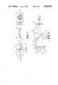
- FIG. 2shows a possible optical arrangement of the millimeter wave signal detecting system discussed above.
- Incident radiation 12 reflected from an object in the field of viewpasses through lens 40, filter 42, a quarter-wave plate 46 to be described subsequently, and polarizing grid 28, after which it is combined with a local oscillator signal emitted by the source of millimeter wave radiation 26.
- the linearly polarized radiation 34 emitted by the sourceis divided by the polarizing grid 28 into major and minor portions 24 and 30 respectively.
- the major portion 24, desirably including about 90% of the millimeter wave energy,passes outwardly as indicated at 48 to illuminate the field of view with millimeter wave radiation.
- the remaining minor portion 30 of the radiation 34 emitted by the source 26is incident on a twist reflector 50. This device, which is described in connection with FIG.
- twist reflector 50reflects the minor component 30 of the radiation back onto the polarizing grid 28, it is then reflected towards the mixer/detector array 36, forming a local oscillator signal 14 for combination with the portion of the illumination beam 24 having been reflected from the field of view.
- the lens 40is generally as described in Goldsmith et al., "Gaussian Optics Lens Antennas", Microwave Journal, Jul. 1984.
- the filter 42is generally as described in Goldsmith, "Designing Quasioptical Systems", in The Microwave System Designers Handbook, Fifth Edition, (1987).
- the filter 42may comprise a metal plate having an array of holes drilled therein to provide a high pass filter for the millimeter wave frequencies of interest.
- the polarizing grid 28may comprise a series of parallel conductors spaced from one another by a dielectric medium.
- the conducting membersmay be spaced parallel wires, e.g., of tungsten coated with gold, spaced in air.
- a less expensive alternativeis to photolithograph flat conductive strips onto a dielectric substrate, e.g., Mylar (TM). In either case, the orientation of the conductors (which are indicated generally at 44 in FIG. 2), with respect to the direction of polarization of the electric field of the millimeter wave energy 34 emitted by the source 26, determines the fraction 24 of the incident millimeter wave energy which is reflected from the grid 28; the remainder 30 passes through the grid 28.
- the spacing of the conductors 44is approximately equal to or less than the wavelength of the millimeter wave radiation emitted by the source 26 divided by five.
- This grid 28transmits the component of the linearly polarized electric field which is perpendicular to the direction of the conductors and reflects the portion which is parallel to their direction. If the conductors 44 are angled with respect to the direction of polarization of the radiation, a corresponding fraction passes through, and the remainder is reflected.
- a quarter-wave plate 46is typically interposed between the polarizing grid 28 and the lens 40.
- the quarter-wave plate 46is a known component which converts a linearly polarized incident wave, such as that emitted by the source 26, into a circularly polarized wave.
- a circularly polarized wavemay have more desirable reflection characteristics from an object to be imaged than the linearly polarized wave; for example, a linearly polarized wave can be reflected asymmetrically depending on the particular orientation of the object, whereas a circularly polarized wave has more uniform reflection characteristics.
- the quarter-wave plate 46Upon reflection of the circularly-polarized wave from the object, the quarter-wave plate 46 will convert it back to a linearly polarized wave, such that it will pass through the polarizing grid 28 without substantial attenuation.
- the quarter-wave platemay be manufactured from crystalline sapphire or by machining appropriate grooves into a dielelectric material such as Rexolite (TM).
- the twist reflector 50comprises a number of generally concave or dish-shaped elements arranged in an array.
- the number of elements in this arrayis equal to the number of elements in the array of millimeter wave emittes making up source 26.
- the shape of the concave elements of the array 50is such as to focus the divergent beams emitted by the elements of the source 26 onto a corresponding area on the surface of the array 36 of mixer/detector elements after reflection from the polarizing grid 28.
- the twist reflector 50comprises a dielectric substrate 56 coated on its rear side with a conductive layer 58, and on its front surface with a series of strips 60 of conductive material oriented at 45° to the direction of polarization of the incident wave.
- the electrical thickness of the dielectric 56is one-quarter wavelength, such that the effective travel distance of the wave through the dielectric is one-half wavelength. Accordingly, when a component 57 of the incident wave 30 which is reflected from the rear conductive layer 58 is combined with a component 59 directly reflected from the strips 60, they will be 180° out of phase. This is equivalent to rotating the direction of polarization of the incident beam by 90°.
- the beam 30 incident on the twist reflector 50(which, it will be recalled, had passed through grid 28) is effectively rotated by 90° with respect to the polarizing grid 28.
- the rotated beamis again incident on grid 28, it is, therefore, reflected onto the array 36.
- the concave elements of the twist reflector 50are square and are fitted into a mosaic, in which as mentioned each element corresponds to one of the emitters of the source 26.
- FIG. 9shows an alternative optical arrangement of the system of the invention in which the twist reflector is eliminated.
- FIG. 4shows a perspective view of a portion of the mixer/detector array 36
- FIG. 5shows schematically a plan view of a portion of a substrate 70 on which conductors 68 making up the individual elements 66 of the array 36 of mixer/detector elements are formed.
- Array 36comprises a plurality of substantially identical mixer/detector elements indicated at 66.
- Each element 66comprises two conductive antenna elements 68 which may be formed directly on a non-conductive dielectric substrate such as Kapton (TM) in turn supported on alumina panels 70, which are spaced from one another by a precision spacer member 72.
- TMKapton
- the outline of a preferred embodiment of the antenna elements 68is shown in FIG. 5.
- the conductive antenna elements 68comprise parallel portions 73 which extend a distance into the array (the incident radiation being received endwise in the view shown), curved portions 74 which approach one another along an exponentially curved outline, and further portions which are separated by a slot 76 and extend for another distance.
- Such an antennais referred to in the art as an "endfire traveling wave slot antenna", as originally described by P. J. Gibson, "The Vivaldi Aerial", Proc. of the European Mic. Conf., Brighton, UK (1979), pp. 101-105.
- Each antennais paired with a nonlinear circuit element 80, e.g. a diode, which provides the mixing function.
- the detector 36may be an array 100 ⁇ 100 of mixer/detector elements 66, resulting in 10,000 identical mixer/detector elements 66 in the overall array 36. This is adequate to provide quite reasonable resolution, for example, to produce an image of a field of view.
- each mixer/detector element 66comprises a paiir of conductors 68, each of which has a relatively thin forward section 73 extending toward the incoming reflected and local oscillator signals, an exponential middle section 74, and a terminal slot 76 separating the two elements 68.
- Mixer diodes 80are connected across the conductors 68, as indicated by FIG. 5.
- slot 76has two additional slots 78 extending from either side thereof and orthogonal thereto. These slots 78 comprise a radio frequency choke which reflects the sum of the local oscillator and detected signals formed upon their mixing, while passing their difference.
- the actual mixing of the local oscillator signal with the signal received from the field of viewis performed by a nonlinear circuit element, e.g., a diode 80, which is preferably physically disposed between the two conductive elements 68 of each element, that is, directly across the slot 76.
- a nonlinear circuit elemente.g., a diode 80
- the diode 80is formed directly on the substrate 70 without separate connecting leads.
- the difference frequency signal which remainsis a relatively "clean" intermediate frequency signal which can be amplified by conventional operational amplifiers 82 associated with each element 66 of the array 36.
- the output signals from amplifiers 82can be supplied directly to the image formation or other radar signal processing circuitry 22 as indicated above.
- FIG. 6shows a cross-sectional view through one of the mixer diodes 80 which are preferably formed directly on the substrate 70 on which are formed the conductors 68 making up each of the antenna elements 66.
- the diode 80comprises bonding pads 84 and 85 which may be formed of gold and extend through vias (that is, through-holes) 86 in a semi-insulating (SI) GaAs substrate 88.
- the gold bonding pads 84 and 85contact further additional gold electrodes 90 and 92 formed on the opposite side of the substrate 88. Electrodes 90 and 92 overlay the actual diode structure.
- the diode structurecomprises a first layer 94 of n + -GaAs which is in contact with the semi-insulating GaAs substrate 88.
- n-GaAs layer 96Over this is formed an n-GaAs layer 96. Atop this layer 96 is provided a layer 98 of Schottky metal, which in a preferred embodiment may be Ti/Pt/Au. The Schottky metal layer 98 is directly in contact with electrode 92 and is thus in contact with bonding pad 84. The n + -GaAs layer 94 is in contact with the other electrode 90 and thus the other bonding pad 85 via an ohmic layer 93 of AuGe/Ni. Finally, an insulating/passivating SiO 2 /Si 3 N 4 material fills spaces 100 and 102 between the various layers.
- Schottky metalwhich in a preferred embodiment may be Ti/Pt/Au.
- the Schottky metal layer 98is directly in contact with electrode 92 and is thus in contact with bonding pad 84.
- the n + -GaAs layer 94is in contact with the other electrode 90 and thus the other bonding pad
- the spaces 100 and 102may also include an air gap between the electrode 92 and the GaAs layers 93 and 94, i.e., around the Schottky metal 98, with or without the SiO 2 /Si 3 N 4 material. This has the beneficial effect of reducing the parasitic capacitance of the mixer diode 80.
- amplifiers 82With that of mixer/detector diodes 80, it may be possible to integrate the function of amplifiers 82 with that of mixer/detector diodes 80. This would require the development of amplifiers capable of operation at millimeter-wave frequencies. It is envisioned that such devices could perform the mixing and amplification functions within a single semiconductive element. This would be highly desirable, as it would presumably substantially increase the signal-to-noise ratio of each mixer/detector element 66. The claims of this application are intended to include such improved devices, when they become available.
- FIG. 7shows a partial end-on view of the emitter array 26, which emits the signal which is mixed with the received signal and which illumiinates the field of view.
- the array 26is made up of a number of substantially identical elements 112.
- the emitter array 26may comprise 625 identical elements 112 in a 25 ⁇ 25 arrangment.
- Each of the individual elements 112 of the array 26, the structure of which is discussed below in connection with FIG. 8,comprises an indium phosphide (InP) Gunn diode or other oscillator coupled to a radiating horn.
- the array 26may be made up of a number of sub-arrays 110 which are integrally fabricated for convenience in manufacturing and assembly.
- FIG. 8is a cross section taken along line 8--8 of FIG. 7, and shows a detail of one of the elements 112 in the source array 26.
- Each elementcomprises a linear osciallator cavity 114 including an integral radiator horn output section.
- the active elementis a Gunn diode element 116, the construction of which is generally conventional.
- the cavitycomprises a radial disc resonator 118 located along a coaxial RF choke structure 119 which supplies DC bias to the Gunn diode element 116.
- a fixed backshort 117is used to optimize the performance of the basic oscillator.
- This type of elementis referred to in the art as a "waveguide cavity resonator" which is driven by the Gunn diode.
- the diode element 116is compressed by a threaded member 120 into the resonator structure 119.
- the center frequency of the Gunn diode oscillatoris determined by the diameter of the resonator disc 118; minor adjustments to its frequency can by provided by mechanical tuning rod 124.
- the bias voltage of the InP Gunn diodecan be varied in order to transmit millimeter wave energy at frequencies varying by approximately ⁇ 300 MHz at 65 GHz. As discussed below, in the preferred embodiment, a "sawtooth" transmitted signal is preferred; to produce this the bias voltage is accordingly varied in a sawtooth fashion. If needed, additonal tuning can be provided by introducing a dielectric material such as sapphire into the vicinity of the resonant disc 118. Typical continuous-wave radiative power levels for the device are 100 mw/emitter at 95 GHz.
- the characteristic atmospheric absorptiondictates operation in either the 1.2 mm, 2 mm or 3 mm wavelength band. Aperture size is reduced for smaller wavelengths, encouraging miniaturization of antenna components, but mixer performance decreases at the higher frequencies concomitant with smaller wavelengths.
- the optimum frequencyis considered to be 94 GHz (3 mm wavelength) or 140 GHz (2 mm), but this could change as better components (principally mixers) become availabe.
- atmospheric attenuationincluding that due to water vapor, need only be considered in connection with very long range imaging systems.
- FIG. 9shows an alternative optical arrangement of the millimeter-wave radar system of the present invention.
- This figureis comparable to FIG. 2, in that it shows the overall arrangement of the device.
- a transmitting array 26located in the focal plane of the lens transmits linearly-polarized millimeter-wave energy onto a polarizing grid 28 which directs it towards a field of view (FOV).
- the transmitted energytravels through a quarter wave plate 46 which transforms it from a linearly polarized beam to a circularly polarized beam.
- the circularly polarized beamis then incident on lens 40' which in this case is a meniscus lens, that is, a concave-convex lens.
- the meniscus lensmay be formed of materials such as Rexolite (TM) or Teflon (TM).
- a portion of the incident radiationis reflected from the lens 40' and becomes the local oscillator signal.
- the precise amount of the radiation reflectedcan be controlled as needed by the employment of known anti-reflective coatings on the surface of lens 40'.
- the remainder of the energy incident on lens 40'is transmitted therethrough to become the illumination beam.
- the quarter-wave plate 46transforms the circularly-polarized reflected local oscillator portion of the beam back into a linearly-polarized beam, but at a polarization of 90° to the original energy, so that is passes through the polarizing grid 28 and is incident on the mixer/detector array 36.
- a high pass filtermay again be employed as indicated at 42.
- the twist reflector 50 of FIG. 2is replaced by the meniscus lens 40', which has the property of passing a major portion of the energy to become the beam which illuminates the field of view while reflecting a minor portion of the energy to become the local oscillator signal which is then incident on array 36.
- the polarizing grid 28need not be aligned with respect to the polarization of the energy from the source array 26 in order to divide the energy into local oscillator and illumination portions; this function is provided by the intrisic characteristics of the mensicus lens 40', optionally in conjunction with an anti-reflective coating as discussed above. Both the local oscillator portion of the incident energy from the source and the energy reflected from objects in the field of view pass twice through the quarter-wave plate. This provides a 90° change in polarization direction, so that the energy passes through the polarizing grid 28 and is incident on the mixer/detector array 36.
- the advantage of this designis that depending on various parameters it may be somewhat simpler to fabricate the meniscus lens than the twist reflector.
- a Faraday rotatorcan be substituted for the quarter wave plate in the embodiment of FIG. 9.
- the Faraday rotatoris described in the Goldsmith article, "Designing Quasioptical Systems", referred to above.
- the Faraday rotatorprovides 45° rotation of the polarization beam such that both the minor local oscillator portion of the emitted energy and the energy reflected from objects in the field of view are rotated through 90° by the Faraday rotator.
- the illumination beamwould be linearly polarized (rather then circularly polarized, as if the quarter-wave plate were used). This may be desirable, depending on the reflection characteristics of the objects to be imaged.
- a further possibilitywould be to provide a Faraday rotator and mirror combination in place of the twist reflector described in connection with FIG. 2. Again this combination would have the function of reflecting the local oscillator portion of the beam and rotating its polarization through 90°, such that on its second incidence on the polarizing grid 28, it would be reflected therefrom and become a local oscillator signal for mixing with the received signal from the field of view in the array of mixer/detector elements 36.
- a millimeter wave signal detection devicewhich comprises an array of mixer/detector elements, each adapted to provide an output intermediate frequency signal responsive to a local oscillator signal mixed with radiation reflected from a portion of a field of view.
- the mixer/detector array according to the inventionis a "staring" array, that is, one which does not require mechanical or electronic scanning in order to provide an image of an entire field of view.
- the output signal from each of the mixer/detector elements of the array 36corresponds to a portion of the device's field of view.
- a detecting devicebe mechanically scanned with respect to the field of view, or that the transmitter by scanned, either by providing a phased-array of emitters or otherwise, in order that a complete image can be generated.
- the transmitting elements according to the inventionilluminate the field of view substantially continually and the detectors each respond to reflection of the transmitted signal from a portion of the field of view. This greatly simplifies generation of an image responsive to reflection of the radar signal from objects in the field of view, and determining their distance, elevation, and azimuth with respect to the system of the invention and measuring their relative velocity.
- the direction of an object from which radiation has been reflectedcan be determined directly responsive to identification of the one or more detector elements which detected the reflected radiation. That is, the postion of the detecting element in the array which detects the reflected signal indicates directly the relative position of the reflecting object with respect to the array.
- Measurement of the distance of the reflecting object from the array, and of its relative velocity with respect to the arraycan be determined using conventional radar signal processing techniques, after the signal has been generated according to the invention.
- conventional radar signal processing techniquesfor example, at pages 81-84 of Skolnik op. cit., (which is incorporated by reference herein) there is provided a brief and succinct but complete description of the way in which distance and velocity information can be derived from reflection of a simple sawtooth varying transmitted signal.
- the distance of the reflecting object from the arrayis determined simply by measuring the transit time taken for the signal to reach the object, be reflected therefrom and be detected at the array, and dividing this time by twice the speed of light c.
- the difference in frequency between the local oscillator signal being transmitted at a particular time and the frequency of the detected signalis directly responsive to the travel time of the reflected signal.
- the travel time of the signalcan be determined proportional to the rate of change of frequency of the transmitted signal.
- Derivation of the relative velocity of the object with respect to the arraycan also readily be derived from relative frequency information contained in the reflected signal, as indicated by Skolnik.
- the relative frequency of the signal reflected from a moving objectvaries with respect to a stationary object at the same azimuth and elevation according to the well known Doppler effect.
- Relative motion of the reflecting object toward the arrayincreases the apparent frequency shift, and motion of the object away from the array decreases the frequency shift.
- This effectcan be distinguished from frequency shift in the reflected signal with respect to the transmitted signal by employment of the sawtooth transmitted signal, and comparison of frequency shift in successive portions thereof.
- this factcan be used in a manner well understood by those of skill in the art to monitor the velocity of objects within the field of view of the system of the invention.
- any of a wide variety of image processing and image enhancement and analysis techinquesmay be combined with the radar signal generation and processing techniques according to the invention, such as convolution, false coloration, and identification of individual objects in the image both by comparison to known shapes and otherwise.
- image signalis provided pixel-by-pixel by the staring array of the invention makes it particularly amenable to many image processing techniques, especially those involving Fourier transformation.
Landscapes
- Engineering & Computer Science (AREA)
- Remote Sensing (AREA)
- Radar, Positioning & Navigation (AREA)
- Physics & Mathematics (AREA)
- General Physics & Mathematics (AREA)
- Computer Networks & Wireless Communication (AREA)
- Electromagnetism (AREA)
- Life Sciences & Earth Sciences (AREA)
- General Life Sciences & Earth Sciences (AREA)
- Geophysics (AREA)
- Radar Systems Or Details Thereof (AREA)
- Geophysics And Detection Of Objects (AREA)
Abstract
Description
Claims (64)
Priority Applications (4)
| Application Number | Priority Date | Filing Date | Title |
|---|---|---|---|
| US07/183,215US4901084A (en) | 1988-04-19 | 1988-04-19 | Object detection and location system |
| US07/286,210US5073782A (en) | 1988-04-19 | 1988-12-19 | Contraband detection system |
| US07/686,841US5202692A (en) | 1986-06-16 | 1991-04-17 | Millimeter wave imaging sensors, sources and systems |
| US07/764,656US5227800A (en) | 1988-04-19 | 1991-09-24 | Contraband detection system |
Applications Claiming Priority (1)
| Application Number | Priority Date | Filing Date | Title |
|---|---|---|---|
| US07/183,215US4901084A (en) | 1988-04-19 | 1988-04-19 | Object detection and location system |
Related Child Applications (2)
| Application Number | Title | Priority Date | Filing Date |
|---|---|---|---|
| US07/286,210Continuation-In-PartUS5073782A (en) | 1987-11-06 | 1988-12-19 | Contraband detection system |
| US07/686,841Continuation-In-PartUS5202692A (en) | 1986-06-16 | 1991-04-17 | Millimeter wave imaging sensors, sources and systems |
Publications (1)
| Publication Number | Publication Date |
|---|---|
| US4901084Atrue US4901084A (en) | 1990-02-13 |
Family
ID=22671938
Family Applications (2)
| Application Number | Title | Priority Date | Filing Date |
|---|---|---|---|
| US07/183,215Expired - LifetimeUS4901084A (en) | 1986-06-16 | 1988-04-19 | Object detection and location system |
| US07/286,210Expired - LifetimeUS5073782A (en) | 1987-11-06 | 1988-12-19 | Contraband detection system |
Family Applications After (1)
| Application Number | Title | Priority Date | Filing Date |
|---|---|---|---|
| US07/286,210Expired - LifetimeUS5073782A (en) | 1987-11-06 | 1988-12-19 | Contraband detection system |
Country Status (1)
| Country | Link |
|---|---|
| US (2) | US4901084A (en) |
Cited By (64)
| Publication number | Priority date | Publication date | Assignee | Title |
|---|---|---|---|---|
| US4994809A (en)* | 1990-03-07 | 1991-02-19 | Hughes Aircraft Company | Polystatic correlating radar |
| US5036748A (en)* | 1988-07-20 | 1991-08-06 | The Marconi Company Limited | Weapon system |
| US5047783A (en)* | 1987-11-06 | 1991-09-10 | Millitech Corporation | Millimeter-wave imaging system |
| EP0386152A4 (en)* | 1987-11-06 | 1991-12-18 | Millitech Corporation | Millimeter wave imaging device |
| US5115245A (en)* | 1990-09-04 | 1992-05-19 | Hughes Aircraft Company | Single substrate microwave radar transceiver including flip-chip integrated circuits |
| US5311603A (en)* | 1992-10-28 | 1994-05-10 | Litton Systems Inc. | Highly efficient superfluorescent fiber laser/amplifier for interferometric sensors |
| US5351077A (en)* | 1992-10-19 | 1994-09-27 | Trw Inc. | Microwave aircraft landing system using narrow bandwidth filtering |
| US5383053A (en)* | 1992-04-07 | 1995-01-17 | Hughes Aircraft Company | Virtual image display having a high efficiency grid beamsplitter |
| US5483455A (en)* | 1992-09-08 | 1996-01-09 | Caterpillar Inc. | Method and apparatus for determining the location of a vehicle |
| EP0690315A3 (en)* | 1994-07-01 | 1996-04-03 | Hughes Aircraft Co | RF sensor and radar for automotive speed and collision avoidance applications |
| US5548637A (en)* | 1993-09-09 | 1996-08-20 | Precision Tracking Fm, Inc. | Method and apparatus for locating personnel and objects in response to telephone inquiries |
| US5580795A (en)* | 1993-08-10 | 1996-12-03 | Loral Vought Systems Corporation | Fabrication method for integrated structure such as photoconductive impedance-matched infrared detector with heterojunction blocking contacts |
| US5734345A (en)* | 1996-04-23 | 1998-03-31 | Trw Inc. | Antenna system for controlling and redirecting communications beams |
| US5760741A (en)* | 1996-04-09 | 1998-06-02 | Trw Inc. | Beam forming network for multiple-beam-feed sharing antenna system |
| US5866965A (en)* | 1991-06-27 | 1999-02-02 | Dana Corporation | Variable reluctance motor having foil wire wound coils |
| US6405127B1 (en) | 2000-09-15 | 2002-06-11 | General Electric Company | Method for determining stationary locomotive location in a railyard |
| US6417797B1 (en) | 1998-07-14 | 2002-07-09 | Cirrus Logic, Inc. | System for A multi-purpose portable imaging device and methods for using same |
| US6447841B1 (en) | 1999-06-02 | 2002-09-10 | International Paper Company | Plastic pigments for durable ink jet paper |
| DE19600609B4 (en)* | 1995-09-30 | 2004-02-19 | Eads Deutschland Gmbh | Polarizer for converting a linearly polarized wave into a circularly polarized wave or into a linearly polarized wave with rotated polarization and vice versa |
| US20040149907A1 (en)* | 2003-01-31 | 2004-08-05 | Vaidya Nitin M. | Offset drift compensating flat fielding method and camera used in millimeter wave imaging |
| US6777684B1 (en) | 1999-08-23 | 2004-08-17 | Rose Research L.L.C. | Systems and methods for millimeter and sub-millimeter wave imaging |
| US6791487B1 (en) | 2003-03-07 | 2004-09-14 | Honeywell International Inc. | Imaging methods and systems for concealed weapon detection |
| US6870162B1 (en) | 2003-01-31 | 2005-03-22 | Millivision, Inc. | Weighted noise compensating method and camera used in millimeter wave imaging |
| US6900438B2 (en) | 2003-01-31 | 2005-05-31 | Millivision Technologies | Baseline compensating method and camera used in millimeter wave imaging |
| US20050122258A1 (en)* | 2003-12-05 | 2005-06-09 | Blasing Raymond R. | Millimeter-wave active imaging system with modular array |
| US20050122249A1 (en)* | 2003-12-05 | 2005-06-09 | Grudkowski Thomas W. | Millimeter-wave active imaging system |
| US20050231416A1 (en)* | 2004-04-14 | 2005-10-20 | Rowe Richard L | Relational millimeter-wave interrogating |
| US20050230604A1 (en)* | 2004-04-14 | 2005-10-20 | Rowe Richard L | Multi-sensor surveillance portal |
| US20050231417A1 (en)* | 2004-04-14 | 2005-10-20 | Michael Fleisher | Surveilled subject privacy imaging |
| US20050231415A1 (en)* | 2004-04-14 | 2005-10-20 | Michael Fleisher | Surveilled subject imaging with object identification |
| US20050232459A1 (en)* | 2004-04-14 | 2005-10-20 | Rowe Richard L | Multi-source surveillance portal |
| US20050231421A1 (en)* | 2004-04-14 | 2005-10-20 | Michael Fleisher | Enhanced surveilled subject imaging |
| US20050232487A1 (en)* | 2004-04-14 | 2005-10-20 | Safeview, Inc. | Active subject privacy imaging |
| US20060097906A1 (en)* | 2003-01-13 | 2006-05-11 | Patric Heide | Radar-transceiver for microwave and millimetre applications |
| US20060104480A1 (en)* | 2004-11-12 | 2006-05-18 | Safeview, Inc. | Active subject imaging with body identification |
| US20060104489A1 (en)* | 2004-08-23 | 2006-05-18 | Bailey Kenneth S | Minutia detection from measurement of a human skull and identifying and profiling individuals from the human skull detection |
| US20060164285A1 (en)* | 2005-01-21 | 2006-07-27 | Safeview, Inc. | Depth-based surveillance imaging |
| US20060164287A1 (en)* | 2005-01-21 | 2006-07-27 | Safeview, Inc. | Depth-based surveillance image reconstruction |
| US20060164286A1 (en)* | 2005-01-21 | 2006-07-27 | Safeview, Inc. | Frequency-based surveillance imaging |
| WO2006090353A1 (en)* | 2005-02-23 | 2006-08-31 | Global Security Devices Ltd. | System and method for detecting concealed objects |
| US7212153B2 (en) | 2003-12-05 | 2007-05-01 | Safeview, Inc. | Millimeter-wave active imaging system with fixed array |
| US20080100510A1 (en)* | 2006-10-27 | 2008-05-01 | Bonthron Andrew J | Method and apparatus for microwave and millimeter-wave imaging |
| RU2326400C1 (en)* | 2007-03-22 | 2008-06-10 | Федеральное государственное учреждение "Федеральный государственный научно-исследовательский испытательный центр радиоэлектронной борьбы и оценки эффективности снижения заметности" Министерства обороны Российской Федерации | Method of measurement of efficient scattering area of large dimension objects in polygon conditions |
| CN100424895C (en)* | 2006-11-24 | 2008-10-08 | 中国科学院上海技术物理研究所 | InGaAs Linear Detector with Micro-Mesa Structure |
| US20090195435A1 (en)* | 2006-06-19 | 2009-08-06 | Ariel-University Research And Develoment Company Ltd. | Hand-held device and method for detecting concealed weapons and hidden objects |
| US20090237092A1 (en)* | 2008-03-20 | 2009-09-24 | The Curators Of The University Of Missouri | Microwave and millimeter wave imaging system |
| US20100045514A1 (en)* | 2007-02-21 | 2010-02-25 | Bernd Bartscher | Device for imaging test objects using electromagnetic waves, in particular for inspecting people for suspicious items |
| US20100090887A1 (en)* | 2008-10-15 | 2010-04-15 | California Institute Of Technology | Multi-pixel high-resolution three-dimensional imaging radar |
| US20100124359A1 (en)* | 2008-03-14 | 2010-05-20 | Vaidya Nitin M | Method and system for automatic detection of a class of objects |
| US20100328142A1 (en)* | 2008-03-20 | 2010-12-30 | The Curators Of The University Of Missouri | Microwave and millimeter wave resonant sensor having perpendicular feed, and imaging system |
| US7973697B2 (en) | 2004-04-14 | 2011-07-05 | L-3 Communications Security And Detection Systems, Inc. | Surveillance systems and methods with subject-related screening |
| US20110254727A1 (en)* | 2010-04-20 | 2011-10-20 | International Business Machines Corporation | Phased array millimeter wave imaging techniques |
| US20120041310A1 (en)* | 2008-09-02 | 2012-02-16 | Arizona Board Of Regents For And On Behalf Of Arizona State University | Apparatus, System and Method for Ultrasound Powered Neurotelemetry |
| US8350747B2 (en) | 2004-04-14 | 2013-01-08 | L-3 Communications Security And Detection Systems, Inc. | Surveillance with subject screening |
| US8681218B1 (en)* | 2008-07-03 | 2014-03-25 | Rockwell Collins, Inc. | System for providing spatial awareness of transmissions of energy in an environment |
| WO2015041502A1 (en)* | 2013-09-23 | 2015-03-26 | 고려대학교 산학협력단 | Image sensing device using radio waves |
| US9046605B2 (en) | 2012-11-05 | 2015-06-02 | The Curators Of The University Of Missouri | Three-dimensional holographical imaging |
| US9700712B2 (en) | 2009-01-26 | 2017-07-11 | Arizona Board Of Regents, A Body Corporate Of The State Of Arizona Acting For And On Behalf Of Arizona State University | Dipolar antenna system and related methods |
| US9871295B2 (en) | 2011-03-25 | 2018-01-16 | Battelle Memorial Institute | Multi-scale, multi-layer diode grid array rectenna |
| US10006993B1 (en)* | 2016-10-27 | 2018-06-26 | Northrop Grumman Systems Corporation | Compact passive millimeter wave (PMMW) camera |
| US20190011534A1 (en)* | 2017-07-07 | 2019-01-10 | Infineon Technologies Ag | System and Method for Identifying a Target Using Radar Sensors |
| US20190056488A1 (en)* | 2017-08-15 | 2019-02-21 | Honeywell International Inc. | Radar using personal phone, tablet, pc for display and interaction |
| CN113960086A (en)* | 2021-09-18 | 2022-01-21 | 中国航天科工集团第二研究院 | Grid collimation imaging system and method for compensation type back scattering detector |
| US12023499B2 (en) | 2014-03-17 | 2024-07-02 | Arizona Board Of Regents On Behalf Of Arizona State University | Methods and systems for measuring tissue impedance and monitoring PVD treatment using neuro-implants with improved ultrasound powering |
Families Citing this family (86)
| Publication number | Priority date | Publication date | Assignee | Title |
|---|---|---|---|---|
| US5990822A (en)* | 1989-04-14 | 1999-11-23 | Honigsbaum; Richard F. | Process and apparatus for finding stealthcraft |
| US5557283A (en)* | 1991-08-30 | 1996-09-17 | Sheen; David M. | Real-time wideband holographic surveillance system |
| US5859609A (en)* | 1991-08-30 | 1999-01-12 | Battelle Memorial Institute | Real-time wideband cylindrical holographic surveillance system |
| US5455590A (en)* | 1991-08-30 | 1995-10-03 | Battelle Memorial Institute | Real-time holographic surveillance system |
| NL9300113A (en)* | 1993-01-21 | 1994-08-16 | Hollandse Signaalapparaten Bv | Radar device. |
| GB9700966D0 (en)* | 1997-01-17 | 1997-03-05 | Secr Defence | Millimetre wave imaging apparatus |
| US7028899B2 (en)* | 1999-06-07 | 2006-04-18 | Metrologic Instruments, Inc. | Method of speckle-noise pattern reduction and apparatus therefore based on reducing the temporal-coherence of the planar laser illumination beam before it illuminates the target object by applying temporal phase modulation techniques during the transmission of the plib towards the target |
| US6218943B1 (en)* | 1998-03-27 | 2001-04-17 | Vivid Technologies, Inc. | Contraband detection and article reclaim system |
| US6208288B1 (en)* | 1998-06-19 | 2001-03-27 | Trw Inc. | Millimeter wave all azimuth field of view surveillance and imaging system |
| US5999122A (en)* | 1998-06-23 | 1999-12-07 | Trw Inc. | Millimeter wave instant photographic camera |
| GB2345750B (en)* | 1998-12-11 | 2002-12-18 | Wicks & Wilson Ltd | Body scanning equipment |
| US7450052B2 (en)* | 1999-05-25 | 2008-11-11 | The Macaleese Companies, Inc. | Object detection method and apparatus |
| US7167123B2 (en)* | 1999-05-25 | 2007-01-23 | Safe Zone Systems, Inc. | Object detection method and apparatus |
| US6342696B1 (en)* | 1999-05-25 | 2002-01-29 | The Macaleese Companies, Inc. | Object detection method and apparatus employing polarized radiation |
| AU2001285167A1 (en)* | 2000-08-23 | 2002-03-04 | Rose Research, L.L.C. | Systems and methods for millimeter and sub-millimeter wave imaging |
| US6473487B1 (en) | 2000-12-27 | 2002-10-29 | Rapiscan Security Products, Inc. | Method and apparatus for physical characteristics discrimination of objects using a limited view three dimensional reconstruction |
| GB0104206D0 (en)* | 2001-02-21 | 2001-04-11 | Secr Defence | Radiometers |
| US6480141B1 (en) | 2001-03-13 | 2002-11-12 | Sandia Corporation | Detection of contraband using microwave radiation |
| US6507309B2 (en) | 2001-03-16 | 2003-01-14 | Battelle Memorial Institute | Interrogation of an object for dimensional and topographical information |
| US6876322B2 (en)* | 2003-06-26 | 2005-04-05 | Battelle Memorial Institute | Concealed object detection |
| US7365672B2 (en)* | 2001-03-16 | 2008-04-29 | Battelle Memorial Institute | Detection of a concealed object |
| US7405692B2 (en)* | 2001-03-16 | 2008-07-29 | Battelle Memorial Institute | Detecting concealed objects at a checkpoint |
| US6563462B1 (en)* | 2001-10-17 | 2003-05-13 | Northrop Grumman Corporation | Millimeter-wave camera for radiometric imaging and communications |
| US6755186B2 (en)* | 2001-10-24 | 2004-06-29 | Honeywell International, Inc. | EGR system flexible gas connection joint |
| GB0204167D0 (en)* | 2002-02-22 | 2002-04-10 | Qinetiq Ltd | Object detection apparatus and method |
| GB0211161D0 (en)* | 2002-05-16 | 2002-06-26 | Qinetiq Ltd | Millimetre-wave illumination source |
| GB0220434D0 (en)* | 2002-09-03 | 2004-03-17 | Qinetiq Ltd | Detection device |
| US7633518B2 (en)* | 2002-10-25 | 2009-12-15 | Quantum Magnetics, Inc. | Object detection portal with video display overlay |
| JP4392661B2 (en)* | 2003-01-16 | 2010-01-06 | 東レ・ファインケミカル株式会社 | Method for recovering optically active diacyltartaric acid |
| AU2004273207B2 (en)* | 2003-09-15 | 2010-03-11 | The Science And Technology Facilities Council | Millimetre and sub-millimetre imaging device |
| US7352180B2 (en)* | 2003-10-02 | 2008-04-01 | Alessandro Manneschi | Magnetic resonance detector for detecting non-authorized materials in footwear |
| WO2005086620A2 (en)* | 2003-10-10 | 2005-09-22 | L-3 Communications Security And Detection Systems | Mmw contraband screening system |
| GB0401389D0 (en)* | 2004-01-22 | 2004-02-25 | Remtons Ltd | Illumination method and apparatus |
| GB2412441A (en)* | 2004-03-26 | 2005-09-28 | Qinetiq Ltd | Imaging apparatus and method |
| GB0407511D0 (en)* | 2004-04-02 | 2004-05-05 | Qinetiq Ltd | Improved millimetre wave illumination system |
| US20080174401A1 (en)* | 2004-04-14 | 2008-07-24 | L-3 Communications Security And Detection Systems, Inc | Surveillance of subject-associated items with identifiers |
| US7253766B2 (en)* | 2004-09-24 | 2007-08-07 | Battelle Memorial Institute | Three-dimensional surface/contour processing based on electromagnetic radiation interrogation |
| US6967612B1 (en)* | 2004-10-22 | 2005-11-22 | Gorman John D | System and method for standoff detection of human carried explosives |
| WO2006055960A2 (en)* | 2004-11-20 | 2006-05-26 | Scenterra, Inc. | Device for emission of high frequency signals |
| US7280078B2 (en)* | 2004-11-20 | 2007-10-09 | Scenterra, Inc. | Sensor for detecting high frequency signals |
| US7709796B2 (en)* | 2005-02-25 | 2010-05-04 | Iscon Video Imaging, Inc. | Methods and systems for detecting presence of materials |
| US7034746B1 (en)* | 2005-03-24 | 2006-04-25 | Bettelle Memorial Institute | Holographic arrays for threat detection and human feature removal |
| US7295146B2 (en)* | 2005-03-24 | 2007-11-13 | Battelle Memorial Institute | Holographic arrays for multi-path imaging artifact reduction |
| EP1886257A1 (en) | 2005-05-11 | 2008-02-13 | Optosecurity Inc. | Method and system for screening luggage items, cargo containers or persons |
| US7991242B2 (en) | 2005-05-11 | 2011-08-02 | Optosecurity Inc. | Apparatus, method and system for screening receptacles and persons, having image distortion correction functionality |
| EP1750147B1 (en) | 2005-08-04 | 2014-04-09 | Alessandro Manneschi | Metal detector |
| RU2294549C1 (en)* | 2005-08-09 | 2007-02-27 | Общество С Ограниченной Ответственностью "Научно-Технический Центр Прикладной Физики" | Method for remote inspection of target in controlled area of space |
| WO2007054685A2 (en)* | 2005-11-09 | 2007-05-18 | Qinetiq Limited | Passive detection apparatus |
| US7298317B2 (en)* | 2005-11-16 | 2007-11-20 | Intellifit Corporation | Gain compensation in an ultra-wideband transceiver |
| ITFI20060098A1 (en)* | 2006-04-28 | 2007-10-29 | Saima Sicurezza Spa | PORTABLE DEVICE FOR DETECTION OF HIDDEN OBJECTS |
| US7899232B2 (en) | 2006-05-11 | 2011-03-01 | Optosecurity Inc. | Method and apparatus for providing threat image projection (TIP) in a luggage screening system, and luggage screening system implementing same |
| US7844081B2 (en)* | 2006-05-15 | 2010-11-30 | Battelle Memorial Institute | Imaging systems and methods for obtaining and using biometric information |
| US7683828B2 (en)* | 2006-07-12 | 2010-03-23 | Enterprise Electronics Corporation | System and method for measuring phase and power variance |
| US8494210B2 (en) | 2007-03-30 | 2013-07-23 | Optosecurity Inc. | User interface for use in security screening providing image enhancement capabilities and apparatus for implementing same |
| GB0617586D0 (en)* | 2006-09-07 | 2006-10-18 | Mbda Uk Ltd | Improvements in or relating to scanners |
| US20080079625A1 (en)* | 2006-10-03 | 2008-04-03 | William Weems | System and method for stereoscopic anomaly detection using microwave imaging |
| JP4963640B2 (en)* | 2006-10-10 | 2012-06-27 | キヤノン株式会社 | Object information acquisition apparatus and method |
| EP2100255A4 (en)* | 2006-12-06 | 2013-12-04 | Kirsen Technologies Corp | SYSTEM AND METHOD FOR DETECTING OBJECTS AND HAZARDOUS SUBSTANCES |
| WO2008109859A1 (en)* | 2007-03-07 | 2008-09-12 | The Macaleese Companies, Inc. D/B/A Safe Zone Systems | Object detection method and apparatus |
| US7830299B2 (en)* | 2007-11-28 | 2010-11-09 | Lockheed Martin Corporation | Radar system for manmade device detection and discrimination from clutter |
| US20100282960A1 (en)* | 2007-12-26 | 2010-11-11 | Clark Keith A | Combined imaging and trace-detection inspection system and method |
| US20090167322A1 (en)* | 2007-12-28 | 2009-07-02 | Erik Edmund Magnuson | Systems and method for classifying a substance |
| CA3018910C (en) | 2008-03-18 | 2020-05-12 | Radio Physics Solutions Limited | Remote detection and measurement of objects |
| US8063813B1 (en)* | 2008-04-14 | 2011-11-22 | Nokomis, Inc. | Active improvised explosive device (IED) electronic signature detection |
| US8035550B2 (en)* | 2008-07-03 | 2011-10-11 | The Boeing Company | Unbalanced non-linear radar |
| US20110102233A1 (en)* | 2008-09-15 | 2011-05-05 | Trex Enterprises Corp. | Active millimeter-wave imaging system |
| GB0916300D0 (en) | 2009-09-17 | 2009-10-28 | Univ Manchester Metropolitan | Remote detection of bladed objects |
| US8835849B1 (en)* | 2010-02-10 | 2014-09-16 | Mvt Equity Llc | Method and apparatus for detection of concealed objects in passive thermal images using environment control |
| JP5617292B2 (en)* | 2010-03-23 | 2014-11-05 | 富士通株式会社 | Transmission / reception apparatus and imaging apparatus |
| EP2697671A2 (en)* | 2011-04-15 | 2014-02-19 | Ariel-University Research and Development Company, Ltd | Passive millimeter-wave detector |
| US20140375335A1 (en)* | 2011-08-26 | 2014-12-25 | Spectral Labs Incorporated | Handheld multisensor contraband detector to improve inspection of personnel at checkpoints |
| KR101973221B1 (en) | 2011-09-07 | 2019-04-26 | 라피스캔 시스템스, 인코포레이티드 | X-ray inspection system that integrates manifest data with imaging/detection processing |
| US9746553B2 (en)* | 2012-12-19 | 2017-08-29 | Sony Corporation | Method for generating an image and handheld screening device |
| DE102013218555A1 (en)* | 2013-07-18 | 2015-01-22 | Rohde & Schwarz Gmbh & Co. Kg | System and method for illuminating and imaging an object |
| US9330330B2 (en)* | 2014-01-15 | 2016-05-03 | Northrop Grumman Systems Corporation | Polarized millimeter wave imaging system and method |
| JP6271384B2 (en)* | 2014-09-19 | 2018-01-31 | 株式会社東芝 | Inspection device |
| US10690760B2 (en)* | 2015-05-05 | 2020-06-23 | Vayyar Imaging Ltd | System and methods for three dimensional modeling of an object using a radio frequency device |
| US9915754B2 (en)* | 2015-05-29 | 2018-03-13 | The Boeing Company | Method and apparatus for detecting energetic materials |
| CN105049071B (en)* | 2015-08-16 | 2017-08-29 | 南京理工大学 | The millimeter wave radiometer receiver and measuring method measured for infrared radiation characteristics |
| CN116309260A (en) | 2016-02-22 | 2023-06-23 | 拉皮斯坎系统股份有限公司 | Method for evaluating average pallet size and density of goods |
| US10473762B2 (en)* | 2016-08-15 | 2019-11-12 | Microsoft Technology Licensing, Llc | Wireless radio module |
| US10448864B1 (en) | 2017-02-24 | 2019-10-22 | Nokomis, Inc. | Apparatus and method to identify and measure gas concentrations |
| US11489847B1 (en) | 2018-02-14 | 2022-11-01 | Nokomis, Inc. | System and method for physically detecting, identifying, and diagnosing medical electronic devices connectable to a network |
| RU2723987C1 (en)* | 2019-07-23 | 2020-06-18 | Роман Евгеньевич Стахно | Method of detection and identification of explosive and narcotic substances and device for its implementation |
| CN110389388B (en)* | 2019-08-06 | 2020-11-13 | 哈尔滨工业大学 | Mechanical linkage scanning passive millimeter wave imaging device |
| US20230408630A1 (en)* | 2022-06-16 | 2023-12-21 | Bae Systems Information And Electronic Systems Integration Inc. | Polarizer assisted star isolation method |
Citations (3)
| Publication number | Priority date | Publication date | Assignee | Title |
|---|---|---|---|---|
| US3746454A (en)* | 1971-03-03 | 1973-07-17 | Us Navy | Infrared receiver for optical radar |
| US4164740A (en)* | 1976-03-04 | 1979-08-14 | Constant James N | Synthetic aperture using image scanner |
| US4611912A (en)* | 1983-04-04 | 1986-09-16 | Ball Corporation | Method and apparatus for optically measuring distance and velocity |
Family Cites Families (8)
| Publication number | Priority date | Publication date | Assignee | Title |
|---|---|---|---|---|
| US3403399A (en)* | 1967-03-10 | 1968-09-24 | Army Usa | Millimeter wave imaging system |
| US4106014A (en)* | 1967-06-26 | 1978-08-08 | The United States Of America As Represented By The Secretary Of The Army | Radar set sensitive to target shape |
| US3772689A (en)* | 1967-12-06 | 1973-11-13 | Us Army | Radar target discrimination method and apparatus |
| US3713156A (en)* | 1970-10-12 | 1973-01-23 | R Pothier | Surface and subsurface detection device |
| US3824593A (en)* | 1972-12-04 | 1974-07-16 | Hughes Aircraft Co | Millimeter wave imaging system using direct carrier injection |
| US3909827A (en)* | 1974-08-30 | 1975-09-30 | Gen Dynamics Corp | Method of and system for microwave interferometry |
| US4521861A (en)* | 1982-04-30 | 1985-06-04 | Texas Instruments Incorporated | Method and apparatus for enhancing radiometric imaging |
| US4754277A (en)* | 1986-09-02 | 1988-06-28 | The Boeing Company | Apparatus and method for producing linear frequency sweep |
- 1988
- 1988-04-19USUS07/183,215patent/US4901084A/ennot_activeExpired - Lifetime
- 1988-12-19USUS07/286,210patent/US5073782A/ennot_activeExpired - Lifetime
Patent Citations (3)
| Publication number | Priority date | Publication date | Assignee | Title |
|---|---|---|---|---|
| US3746454A (en)* | 1971-03-03 | 1973-07-17 | Us Navy | Infrared receiver for optical radar |
| US4164740A (en)* | 1976-03-04 | 1979-08-14 | Constant James N | Synthetic aperture using image scanner |
| US4611912A (en)* | 1983-04-04 | 1986-09-16 | Ball Corporation | Method and apparatus for optically measuring distance and velocity |
Non-Patent Citations (14)
| Title |
|---|
| Goldsmith, P. F., "Designing Quasioptical Systems" (5th Edition), Microwave System Designers Handbook (1987). |
| Goldsmith, P. F., Designing Quasioptical Systems (5th Edition), Microwave System Designers Handbook (1987).* |
| Korzeniowski et al., "Imaging System at 946HZ Using Tuperev Slot Antennu Elements", Eighth IEEE Int'l. Conference on Infrared and Millimeter Waves (1983). |
| Korzeniowski et al., Imaging System at 946HZ Using Tuperev Slot Antennu Elements , Eighth IEEE Int l. Conference on Infrared and Millimeter Waves (1983).* |
| Singh et al., "Integrated 946HZ Transceiver with InP Gunn Diode Local Oscillator", Government Microelectronics and Circuits Conference (1986), pp. 295-297. |
| Singh et al., Integrated 946HZ Transceiver with InP Gunn Diode Local Oscillator , Government Microelectronics and Circuits Conference (1986), pp. 295 297.* |
| Skolnik, Introduction to Radar Systems (1980), pp. 81 84.* |
| Skolnik, Introduction to Radar Systems (1980), pp. 81-84. |
| Yngvesson et al., "Millimeter Wave Imaging System with an Endfire Receptor Array" Tenth Int'l. Conf. On Infrared and Millimeter Waves (1981). |
| Yngvesson et al., Millimeter Wave Imaging System with an Endfire Receptor Array Tenth Int l. Conf. On Infrared and Millimeter Waves (1981).* |
| Yngvesson, "Imaging Front-End Systems for Millimeter Waves on Submillimeter Waves", SPIE Conf. on Submillimeter Spectroscopy, (1985). |
| Yngvesson, "Near Millimeter Imaging with Integrated Planar Receptors: General Requirements and Constraints", Infrared and Millimeter Waves, 10, pp. 91-110 (1983). |
| Yngvesson, Imaging Front End Systems for Millimeter Waves on Submillimeter Waves , SPIE Conf. on Submillimeter Spectroscopy, (1985).* |
| Yngvesson, Near Millimeter Imaging with Integrated Planar Receptors: General Requirements and Constraints , Infrared and Millimeter Waves, 10, pp. 91 110 (1983).* |
Cited By (100)
| Publication number | Priority date | Publication date | Assignee | Title |
|---|---|---|---|---|
| US5047783A (en)* | 1987-11-06 | 1991-09-10 | Millitech Corporation | Millimeter-wave imaging system |
| EP0386152A4 (en)* | 1987-11-06 | 1991-12-18 | Millitech Corporation | Millimeter wave imaging device |
| US5036748A (en)* | 1988-07-20 | 1991-08-06 | The Marconi Company Limited | Weapon system |
| US4994809A (en)* | 1990-03-07 | 1991-02-19 | Hughes Aircraft Company | Polystatic correlating radar |
| US5115245A (en)* | 1990-09-04 | 1992-05-19 | Hughes Aircraft Company | Single substrate microwave radar transceiver including flip-chip integrated circuits |
| EP0474393A3 (en)* | 1990-09-04 | 1992-10-21 | Hughes Aircraft Company | Single substrate microwave radar transceiver including flip-chip integrated circuits |
| US5866965A (en)* | 1991-06-27 | 1999-02-02 | Dana Corporation | Variable reluctance motor having foil wire wound coils |
| US5383053A (en)* | 1992-04-07 | 1995-01-17 | Hughes Aircraft Company | Virtual image display having a high efficiency grid beamsplitter |
| US5483455A (en)* | 1992-09-08 | 1996-01-09 | Caterpillar Inc. | Method and apparatus for determining the location of a vehicle |
| US5351077A (en)* | 1992-10-19 | 1994-09-27 | Trw Inc. | Microwave aircraft landing system using narrow bandwidth filtering |
| US5311603A (en)* | 1992-10-28 | 1994-05-10 | Litton Systems Inc. | Highly efficient superfluorescent fiber laser/amplifier for interferometric sensors |
| US5580795A (en)* | 1993-08-10 | 1996-12-03 | Loral Vought Systems Corporation | Fabrication method for integrated structure such as photoconductive impedance-matched infrared detector with heterojunction blocking contacts |
| US5548637A (en)* | 1993-09-09 | 1996-08-20 | Precision Tracking Fm, Inc. | Method and apparatus for locating personnel and objects in response to telephone inquiries |
| EP0690315A3 (en)* | 1994-07-01 | 1996-04-03 | Hughes Aircraft Co | RF sensor and radar for automotive speed and collision avoidance applications |
| DE19600609B4 (en)* | 1995-09-30 | 2004-02-19 | Eads Deutschland Gmbh | Polarizer for converting a linearly polarized wave into a circularly polarized wave or into a linearly polarized wave with rotated polarization and vice versa |
| US5760741A (en)* | 1996-04-09 | 1998-06-02 | Trw Inc. | Beam forming network for multiple-beam-feed sharing antenna system |
| US5734345A (en)* | 1996-04-23 | 1998-03-31 | Trw Inc. | Antenna system for controlling and redirecting communications beams |
| US6417797B1 (en) | 1998-07-14 | 2002-07-09 | Cirrus Logic, Inc. | System for A multi-purpose portable imaging device and methods for using same |
| US6447841B1 (en) | 1999-06-02 | 2002-09-10 | International Paper Company | Plastic pigments for durable ink jet paper |
| US6777684B1 (en) | 1999-08-23 | 2004-08-17 | Rose Research L.L.C. | Systems and methods for millimeter and sub-millimeter wave imaging |
| US6405127B1 (en) | 2000-09-15 | 2002-06-11 | General Electric Company | Method for determining stationary locomotive location in a railyard |
| US20060097906A1 (en)* | 2003-01-13 | 2006-05-11 | Patric Heide | Radar-transceiver for microwave and millimetre applications |
| US6870162B1 (en) | 2003-01-31 | 2005-03-22 | Millivision, Inc. | Weighted noise compensating method and camera used in millimeter wave imaging |
| US7075080B2 (en) | 2003-01-31 | 2006-07-11 | Millivision Technologies | Offset drift compensating flat fielding method and camera used in millimeter wave imaging |
| US6878939B2 (en) | 2003-01-31 | 2005-04-12 | Millivision Technologies | Offset drift compensating flat fielding method and camera used in millimeter wave imaging |
| US6900438B2 (en) | 2003-01-31 | 2005-05-31 | Millivision Technologies | Baseline compensating method and camera used in millimeter wave imaging |
| US20060006322A1 (en)* | 2003-01-31 | 2006-01-12 | Vaidya Nitin M | Weighted noise compensating method and camera used in millimeter wave imaging |
| US20060022128A1 (en)* | 2003-01-31 | 2006-02-02 | Vaidya Nitin M | Baseline compensating method and camera used in millimeter wave imaging |
| US20050151080A1 (en)* | 2003-01-31 | 2005-07-14 | Vaidya Nitin M. | Offset drift compensating flat fielding method and camera used in millimeter wave imaging |
| US20040149907A1 (en)* | 2003-01-31 | 2004-08-05 | Vaidya Nitin M. | Offset drift compensating flat fielding method and camera used in millimeter wave imaging |
| US7132649B2 (en) | 2003-01-31 | 2006-11-07 | Vaidya Nitin M | Weighted noise compensating method and camera used in millimeter wave imaging |
| US6791487B1 (en) | 2003-03-07 | 2004-09-14 | Honeywell International Inc. | Imaging methods and systems for concealed weapon detection |
| US7212153B2 (en) | 2003-12-05 | 2007-05-01 | Safeview, Inc. | Millimeter-wave active imaging system with fixed array |
| US7119740B2 (en) | 2003-12-05 | 2006-10-10 | Safeview, Inc. | Millimeter-wave active imaging system with modular array |
| US6992616B2 (en) | 2003-12-05 | 2006-01-31 | Safeview, Inc. | Millimeter-wave active imaging system |
| US20050122249A1 (en)* | 2003-12-05 | 2005-06-09 | Grudkowski Thomas W. | Millimeter-wave active imaging system |
| US20050122258A1 (en)* | 2003-12-05 | 2005-06-09 | Blasing Raymond R. | Millimeter-wave active imaging system with modular array |
| US7123185B2 (en) | 2004-04-14 | 2006-10-17 | Safeview, Inc. | Enhanced surveilled subject imaging |
| US20050231415A1 (en)* | 2004-04-14 | 2005-10-20 | Michael Fleisher | Surveilled subject imaging with object identification |
| US20050231421A1 (en)* | 2004-04-14 | 2005-10-20 | Michael Fleisher | Enhanced surveilled subject imaging |
| US20080043102A1 (en)* | 2004-04-14 | 2008-02-21 | Safeview, Inc. | Multi-source surveillance system |
| US7265709B2 (en) | 2004-04-14 | 2007-09-04 | Safeview, Inc. | Surveilled subject imaging with object identification |
| US20050232459A1 (en)* | 2004-04-14 | 2005-10-20 | Rowe Richard L | Multi-source surveillance portal |
| US20050232487A1 (en)* | 2004-04-14 | 2005-10-20 | Safeview, Inc. | Active subject privacy imaging |
| US20050231416A1 (en)* | 2004-04-14 | 2005-10-20 | Rowe Richard L | Relational millimeter-wave interrogating |
| US7973697B2 (en) | 2004-04-14 | 2011-07-05 | L-3 Communications Security And Detection Systems, Inc. | Surveillance systems and methods with subject-related screening |
| US8345918B2 (en) | 2004-04-14 | 2013-01-01 | L-3 Communications Corporation | Active subject privacy imaging |
| US7528763B2 (en) | 2004-04-14 | 2009-05-05 | Safeview, Inc. | Millimeter-wave interrogation relating features |
| US7205926B2 (en) | 2004-04-14 | 2007-04-17 | Safeview, Inc. | Multi-source surveillance system |
| US20050231417A1 (en)* | 2004-04-14 | 2005-10-20 | Michael Fleisher | Surveilled subject privacy imaging |
| US20050230604A1 (en)* | 2004-04-14 | 2005-10-20 | Rowe Richard L | Multi-sensor surveillance portal |
| US8350747B2 (en) | 2004-04-14 | 2013-01-08 | L-3 Communications Security And Detection Systems, Inc. | Surveillance with subject screening |
| US20060279451A1 (en)* | 2004-04-14 | 2006-12-14 | Safeview, Inc. | Millimeter-wave interrogation relating features |
| US7180441B2 (en) | 2004-04-14 | 2007-02-20 | Safeview, Inc. | Multi-sensor surveillance portal |
| US7202808B2 (en) | 2004-04-14 | 2007-04-10 | Safeview, Inc. | Surveilled subject privacy imaging |
| US7616797B2 (en)* | 2004-08-23 | 2009-11-10 | Bailey Kenneth S | Minutia detection from measurement of a human skull and identifying and profiling individuals from the human skull detection |
| US20060104489A1 (en)* | 2004-08-23 | 2006-05-18 | Bailey Kenneth S | Minutia detection from measurement of a human skull and identifying and profiling individuals from the human skull detection |
| US7386150B2 (en) | 2004-11-12 | 2008-06-10 | Safeview, Inc. | Active subject imaging with body identification |
| US20060104480A1 (en)* | 2004-11-12 | 2006-05-18 | Safeview, Inc. | Active subject imaging with body identification |
| US20060164286A1 (en)* | 2005-01-21 | 2006-07-27 | Safeview, Inc. | Frequency-based surveillance imaging |
| US7145506B2 (en) | 2005-01-21 | 2006-12-05 | Safeview, Inc. | Depth-based surveillance image reconstruction |
| US7119731B2 (en) | 2005-01-21 | 2006-10-10 | Safeview, Inc. | Depth-based surveillance imaging |
| US20060164287A1 (en)* | 2005-01-21 | 2006-07-27 | Safeview, Inc. | Depth-based surveillance image reconstruction |
| US20060164285A1 (en)* | 2005-01-21 | 2006-07-27 | Safeview, Inc. | Depth-based surveillance imaging |
| WO2006090353A1 (en)* | 2005-02-23 | 2006-08-31 | Global Security Devices Ltd. | System and method for detecting concealed objects |
| US20090195435A1 (en)* | 2006-06-19 | 2009-08-06 | Ariel-University Research And Develoment Company Ltd. | Hand-held device and method for detecting concealed weapons and hidden objects |
| US20080100510A1 (en)* | 2006-10-27 | 2008-05-01 | Bonthron Andrew J | Method and apparatus for microwave and millimeter-wave imaging |
| WO2008057286A3 (en)* | 2006-10-27 | 2008-08-07 | Clariant Technologies Corp | Method and apparatus for microwave and millimeter-wave imaging |
| CN100424895C (en)* | 2006-11-24 | 2008-10-08 | 中国科学院上海技术物理研究所 | InGaAs Linear Detector with Micro-Mesa Structure |
| US20100045514A1 (en)* | 2007-02-21 | 2010-02-25 | Bernd Bartscher | Device for imaging test objects using electromagnetic waves, in particular for inspecting people for suspicious items |
| US8169355B2 (en)* | 2007-02-21 | 2012-05-01 | Smiths Heimann Gmbh | Device for imaging test objects using electromagnetic waves, in particular for inspecting people for suspicious items |
| RU2326400C1 (en)* | 2007-03-22 | 2008-06-10 | Федеральное государственное учреждение "Федеральный государственный научно-исследовательский испытательный центр радиоэлектронной борьбы и оценки эффективности снижения заметности" Министерства обороны Российской Федерации | Method of measurement of efficient scattering area of large dimension objects in polygon conditions |
| US8774461B2 (en) | 2008-03-14 | 2014-07-08 | Mvt Equity Llc | Method and system for automatic detection of a class of objects |
| US20100124359A1 (en)* | 2008-03-14 | 2010-05-20 | Vaidya Nitin M | Method and system for automatic detection of a class of objects |
| US8224021B2 (en) | 2008-03-14 | 2012-07-17 | Millivision Technologies, Inc. | Method and system for automatic detection of a class of objects |
| US7746266B2 (en)* | 2008-03-20 | 2010-06-29 | The Curators Of The University Of Missouri | Microwave and millimeter wave imaging system |
| US20100328142A1 (en)* | 2008-03-20 | 2010-12-30 | The Curators Of The University Of Missouri | Microwave and millimeter wave resonant sensor having perpendicular feed, and imaging system |
| US20090237092A1 (en)* | 2008-03-20 | 2009-09-24 | The Curators Of The University Of Missouri | Microwave and millimeter wave imaging system |
| US8681218B1 (en)* | 2008-07-03 | 2014-03-25 | Rockwell Collins, Inc. | System for providing spatial awareness of transmissions of energy in an environment |
| US20120041310A1 (en)* | 2008-09-02 | 2012-02-16 | Arizona Board Of Regents For And On Behalf Of Arizona State University | Apparatus, System and Method for Ultrasound Powered Neurotelemetry |
| US20100090887A1 (en)* | 2008-10-15 | 2010-04-15 | California Institute Of Technology | Multi-pixel high-resolution three-dimensional imaging radar |
| US8144052B2 (en)* | 2008-10-15 | 2012-03-27 | California Institute Of Technology | Multi-pixel high-resolution three-dimensional imaging radar |
| US9700712B2 (en) | 2009-01-26 | 2017-07-11 | Arizona Board Of Regents, A Body Corporate Of The State Of Arizona Acting For And On Behalf Of Arizona State University | Dipolar antenna system and related methods |
| US10463856B2 (en) | 2009-05-22 | 2019-11-05 | Arizona Board Of Regents On Behalf Of Arizona State University | Dipolar antenna system and related methods |
| US11497907B2 (en) | 2009-05-22 | 2022-11-15 | Arizona Board Of Regents On Behalf Of Arizona State University | Dipolar antenna system and related methods |
| US8456351B2 (en)* | 2010-04-20 | 2013-06-04 | International Business Machines Corporation | Phased array millimeter wave imaging techniques |
| US20110254727A1 (en)* | 2010-04-20 | 2011-10-20 | International Business Machines Corporation | Phased array millimeter wave imaging techniques |
| US9871295B2 (en) | 2011-03-25 | 2018-01-16 | Battelle Memorial Institute | Multi-scale, multi-layer diode grid array rectenna |
| US9046605B2 (en) | 2012-11-05 | 2015-06-02 | The Curators Of The University Of Missouri | Three-dimensional holographical imaging |
| WO2015041502A1 (en)* | 2013-09-23 | 2015-03-26 | 고려대학교 산학협력단 | Image sensing device using radio waves |
| US12023499B2 (en) | 2014-03-17 | 2024-07-02 | Arizona Board Of Regents On Behalf Of Arizona State University | Methods and systems for measuring tissue impedance and monitoring PVD treatment using neuro-implants with improved ultrasound powering |
| US10006993B1 (en)* | 2016-10-27 | 2018-06-26 | Northrop Grumman Systems Corporation | Compact passive millimeter wave (PMMW) camera |
| US10591586B2 (en)* | 2017-07-07 | 2020-03-17 | Infineon Technologies Ag | System and method for identifying a target using radar sensors |
| US11656333B2 (en) | 2017-07-07 | 2023-05-23 | Infineon Technologies Ag | System and method for identifying a target using radar sensors |
| US20190011534A1 (en)* | 2017-07-07 | 2019-01-10 | Infineon Technologies Ag | System and Method for Identifying a Target Using Radar Sensors |
| US10712438B2 (en)* | 2017-08-15 | 2020-07-14 | Honeywell International Inc. | Radar using personal phone, tablet, PC for display and interaction |
| US20190056488A1 (en)* | 2017-08-15 | 2019-02-21 | Honeywell International Inc. | Radar using personal phone, tablet, pc for display and interaction |
| US11906617B2 (en) | 2017-08-15 | 2024-02-20 | Honeywell International Inc. | Radar using personal phone, tablet, PC for display and interaction |
| CN113960086A (en)* | 2021-09-18 | 2022-01-21 | 中国航天科工集团第二研究院 | Grid collimation imaging system and method for compensation type back scattering detector |
| CN113960086B (en)* | 2021-09-18 | 2024-01-02 | 中国航天科工集团第二研究院 | Compensation type back scattering detector grid collimation imaging system and method |
Also Published As
| Publication number | Publication date |
|---|---|
| US5073782A (en) | 1991-12-17 |
Similar Documents
| Publication | Publication Date | Title |
|---|---|---|
| US4901084A (en) | Object detection and location system | |
| CA1325258C (en) | Millimeter wave imaging device | |
| US5227800A (en) | Contraband detection system | |
| US5455589A (en) | Compact microwave and millimeter wave radar | |
| Menzel et al. | A 77-GHz FM/CW radar front-end with a low-profile low-loss printed antenna | |
| US5202692A (en) | Millimeter wave imaging sensors, sources and systems | |
| EP0690315B1 (en) | RF sensor and radar for automotive speed and collision avoidance applications | |
| US6943742B2 (en) | Focal plane array for THz imager and associated methods | |
| US5982326A (en) | Active micropatch antenna device and array system | |
| McMillan et al. | An experimental 225 GHz pulsed coherent radar | |
| US7460060B2 (en) | Electromagnetic wave transmitting/receiving module and imaging sensor having electromagnetic wave transmitting/receiving module | |
| Uehara et al. | Lens-coupled imaging arrays for the millimeter-and submillimeter-wave regions | |
| EP0012055B1 (en) | Microstrip monopulse primary feed and antenna using same | |
| JP3534410B2 (en) | Radiation sensor | |
| FR2930079A1 (en) | RADIATION SENSOR, IN PARTICULAR FOR RADAR | |
| Skalare et al. | A planar dipole array antenna with an elliptical lens | |
| US5248977A (en) | One-dimensional electronic image scanner | |
| US3970839A (en) | Generating and using coherent optical radiation | |
| US4020341A (en) | Generating and using coherent optical radiation | |
| Basu et al. | Millimeter-wave antennas | |
| CA1329659C (en) | Millimeter wave imaging sensors, sources, and systems | |
| JPH05107337A (en) | Pulse radar and its components | |
| GB2235585A (en) | A multiple-beam antenna system | |
| Bischoff et al. | Concepts for a Submm Array Receiver | |
| Emerson et al. | U. BISCHOFF, R. NITSCH, J. HORN, K. JACOBS, R. SCHIEDER |
Legal Events
| Date | Code | Title | Description |
|---|---|---|---|
| AS | Assignment | Owner name:MILLITECH CORPORATION, A CORP. OF MA Free format text:ASSIGNMENT OF ASSIGNORS INTEREST.;ASSIGNORS:HUGUENIN, G. RICHARD;GOLDSMITH, PAUL F.;REEL/FRAME:004941/0336;SIGNING DATES FROM 19880422 TO 19880506 Owner name:MILLITECH CORPORATION, A CORP. OF MA Free format text:ASSIGNMENT OF ASSIGNORS INTEREST.;ASSIGNORS:DEO, NARESH C.;WALKER, DAVID K.;REEL/FRAME:004941/0335 Effective date:19880505 | |
| STCF | Information on status: patent grant | Free format text:PATENTED CASE | |
| AS | Assignment | Owner name:SHAWMUT BANK, N.A.,, MASSACHUSETTS Free format text:SECURITY INTEREST;ASSIGNOR:MILLITECH CORPORATION;REEL/FRAME:005811/0036 Effective date:19910718 | |
| CC | Certificate of correction | ||
| FPAY | Fee payment | Year of fee payment:4 | |
| AS | Assignment | Owner name:MILLITECH CORPORATION, MASSACHUSETTS Free format text:RELEASE BY SECURED PARTY;ASSIGNOR:SHAWMUT BANK, N.A.;REEL/FRAME:006763/0127 Effective date:19930816 | |
| AS | Assignment | Owner name:SILICON VALLEY BANK, CALIFORNIA Free format text:CONVEYANCE OF PATENT & TRADEMARKS;ASSIGNOR:MILLITECH CORPORATION;REEL/FRAME:006767/0016 Effective date:19930421 | |
| FEPP | Fee payment procedure | Free format text:PAYOR NUMBER ASSIGNED (ORIGINAL EVENT CODE: ASPN); ENTITY STATUS OF PATENT OWNER: LARGE ENTITY | |
| FPAY | Fee payment | Year of fee payment:8 | |
| FEPP | Fee payment procedure | Free format text:PAT HLDR NO LONGER CLAIMS SMALL ENT STAT AS SMALL BUSINESS (ORIGINAL EVENT CODE: LSM2); ENTITY STATUS OF PATENT OWNER: LARGE ENTITY Free format text:PAYER NUMBER DE-ASSIGNED (ORIGINAL EVENT CODE: RMPN); ENTITY STATUS OF PATENT OWNER: LARGE ENTITY Free format text:PAYOR NUMBER ASSIGNED (ORIGINAL EVENT CODE: ASPN); ENTITY STATUS OF PATENT OWNER: LARGE ENTITY | |
| REFU | Refund | Free format text:REFUND - PAYMENT OF MAINTENANCE FEE, 12TH YR, SMALL ENTITY (ORIGINAL EVENT CODE: R285); ENTITY STATUS OF PATENT OWNER: LARGE ENTITY | |
| FPAY | Fee payment | Year of fee payment:12 | |
| AS | Assignment | Owner name:MLV EQUITY LLC, NEW YORK Free format text:ASSIGNMENT OF ASSIGNORS INTEREST;ASSIGNOR:YDI WIRELESS, INC. (F/K/A TELAXIS COMMUNICATIONS CORPORATION AND MILLITECH CORPORATION);REEL/FRAME:014384/0744 Effective date:20040225 | |
| AS | Assignment | Owner name:MVT EQUITY LLC, NEW YORK Free format text:MERGER;ASSIGNOR:MLV EQUITY LLC;REEL/FRAME:015583/0536 Effective date:20040225 |