US4893094A - Frequency synthesizer with control of start-up battery saving operations - Google Patents
Frequency synthesizer with control of start-up battery saving operationsDownload PDFInfo
- Publication number
- US4893094A US4893094AUS07/322,393US32239389AUS4893094AUS 4893094 AUS4893094 AUS 4893094AUS 32239389 AUS32239389 AUS 32239389AUS 4893094 AUS4893094 AUS 4893094A
- Authority
- US
- United States
- Prior art keywords
- signal
- frequency
- battery saving
- awake
- signals
- Prior art date
- Legal status (The legal status is an assumption and is not a legal conclusion. Google has not performed a legal analysis and makes no representation as to the accuracy of the status listed.)
- Expired - Lifetime
Links
- 230000004044responseEffects0.000claimsabstractdescription12
- 239000003990capacitorSubstances0.000claimsdescription15
- 238000012358sourcingMethods0.000claimsdescription12
- 238000012360testing methodMethods0.000claimsdescription4
- 230000002401inhibitory effectEffects0.000claimsdescription3
- 230000002708enhancing effectEffects0.000abstractdescription3
- 230000000694effectsEffects0.000description8
- 230000003321amplificationEffects0.000description4
- 238000003199nucleic acid amplification methodMethods0.000description4
- 230000000295complement effectEffects0.000description3
- 238000000034methodMethods0.000description3
- 230000000737periodic effectEffects0.000description3
- 230000006399behaviorEffects0.000description2
- 238000010586diagramMethods0.000description2
- 238000007792additionMethods0.000description1
- 238000013459approachMethods0.000description1
- 238000013461designMethods0.000description1
- 238000001514detection methodMethods0.000description1
- 238000012986modificationMethods0.000description1
- 230000004048modificationEffects0.000description1
- 210000000056organAnatomy0.000description1
- 230000006641stabilisationEffects0.000description1
- 238000011105stabilizationMethods0.000description1
- 230000007704transitionEffects0.000description1
Images


Classifications
- H—ELECTRICITY
- H03—ELECTRONIC CIRCUITRY
- H03L—AUTOMATIC CONTROL, STARTING, SYNCHRONISATION OR STABILISATION OF GENERATORS OF ELECTRONIC OSCILLATIONS OR PULSES
- H03L7/00—Automatic control of frequency or phase; Synchronisation
- H03L7/06—Automatic control of frequency or phase; Synchronisation using a reference signal applied to a frequency- or phase-locked loop
- H03L7/16—Indirect frequency synthesis, i.e. generating a desired one of a number of predetermined frequencies using a frequency- or phase-locked loop
- H03L7/18—Indirect frequency synthesis, i.e. generating a desired one of a number of predetermined frequencies using a frequency- or phase-locked loop using a frequency divider or counter in the loop
- H03L7/183—Indirect frequency synthesis, i.e. generating a desired one of a number of predetermined frequencies using a frequency- or phase-locked loop using a frequency divider or counter in the loop a time difference being used for locking the loop, the counter counting between fixed numbers or the frequency divider dividing by a fixed number
- H—ELECTRICITY
- H03—ELECTRONIC CIRCUITRY
- H03L—AUTOMATIC CONTROL, STARTING, SYNCHRONISATION OR STABILISATION OF GENERATORS OF ELECTRONIC OSCILLATIONS OR PULSES
- H03L7/00—Automatic control of frequency or phase; Synchronisation
- H03L7/06—Automatic control of frequency or phase; Synchronisation using a reference signal applied to a frequency- or phase-locked loop
- H03L7/16—Indirect frequency synthesis, i.e. generating a desired one of a number of predetermined frequencies using a frequency- or phase-locked loop
- H03L7/18—Indirect frequency synthesis, i.e. generating a desired one of a number of predetermined frequencies using a frequency- or phase-locked loop using a frequency divider or counter in the loop
- H—ELECTRICITY
- H03—ELECTRONIC CIRCUITRY
- H03L—AUTOMATIC CONTROL, STARTING, SYNCHRONISATION OR STABILISATION OF GENERATORS OF ELECTRONIC OSCILLATIONS OR PULSES
- H03L3/00—Starting of generators
- H—ELECTRICITY
- H03—ELECTRONIC CIRCUITRY
- H03L—AUTOMATIC CONTROL, STARTING, SYNCHRONISATION OR STABILISATION OF GENERATORS OF ELECTRONIC OSCILLATIONS OR PULSES
- H03L7/00—Automatic control of frequency or phase; Synchronisation
- H03L7/06—Automatic control of frequency or phase; Synchronisation using a reference signal applied to a frequency- or phase-locked loop
- H03L7/08—Details of the phase-locked loop
- H03L7/0802—Details of the phase-locked loop the loop being adapted for reducing power consumption
- H—ELECTRICITY
- H03—ELECTRONIC CIRCUITRY
- H03L—AUTOMATIC CONTROL, STARTING, SYNCHRONISATION OR STABILISATION OF GENERATORS OF ELECTRONIC OSCILLATIONS OR PULSES
- H03L7/00—Automatic control of frequency or phase; Synchronisation
- H03L7/06—Automatic control of frequency or phase; Synchronisation using a reference signal applied to a frequency- or phase-locked loop
- H03L7/08—Details of the phase-locked loop
- H03L7/10—Details of the phase-locked loop for assuring initial synchronisation or for broadening the capture range
- H03L7/107—Details of the phase-locked loop for assuring initial synchronisation or for broadening the capture range using a variable transfer function for the loop, e.g. low pass filter having a variable bandwidth
- H03L7/1072—Details of the phase-locked loop for assuring initial synchronisation or for broadening the capture range using a variable transfer function for the loop, e.g. low pass filter having a variable bandwidth by changing characteristics of the charge pump, e.g. changing the gain
- H—ELECTRICITY
- H03—ELECTRONIC CIRCUITRY
- H03L—AUTOMATIC CONTROL, STARTING, SYNCHRONISATION OR STABILISATION OF GENERATORS OF ELECTRONIC OSCILLATIONS OR PULSES
- H03L7/00—Automatic control of frequency or phase; Synchronisation
- H03L7/06—Automatic control of frequency or phase; Synchronisation using a reference signal applied to a frequency- or phase-locked loop
- H03L7/08—Details of the phase-locked loop
- H03L7/085—Details of the phase-locked loop concerning mainly the frequency- or phase-detection arrangement including the filtering or amplification of its output signal
- H03L7/089—Details of the phase-locked loop concerning mainly the frequency- or phase-detection arrangement including the filtering or amplification of its output signal the phase or frequency detector generating up-down pulses
- H03L7/0891—Details of the phase-locked loop concerning mainly the frequency- or phase-detection arrangement including the filtering or amplification of its output signal the phase or frequency detector generating up-down pulses the up-down pulses controlling source and sink current generators, e.g. a charge pump
- H03L7/0895—Details of the current generators
- H03L7/0898—Details of the current generators the source or sink current values being variable
Definitions
- the present inventionrelates to a frequency synthesizer which is governed over time in accordance with sleep and awake cycles of a battery saving signal, and more particularly, to a control circuit coupled to the frequency synthesizer for enhancing the start-up operational behavior thereof with regard to the sleep and awake battery saving cycles.
- a frequency synthesizermay be used in a radio receiver, for example, to generate a channel frequency signal which is used in a demodulator section to pass received information signals only within a desired channel represented by the generated channel frequency signal.
- Other applications of a frequency synthesizerinclude tone generating circuits for an electronic organ and oscillator circuits for controlling the operational frequency of a microprocessor, for example.
- a frequency synthesizergenerally includes a reference oscillator which generates a very stable reference frequency signal and another oscillator which is controlled by a voltage potential to generate the channel frequency signal.
- a feedback frequency signalis developed from the channel frequency signal via a divide by N circuit.
- a phase detector circuitoperates to converge the phase of the feedback frequency signal to the phase of the reference frequency signal by adjusting the governing voltage potential of the voltage controlled oscillator.
- the elements of the phase detector, the voltage controlled oscillator, and the divide by N counterconstitute, in combination, what is generally referred to as a phase locked loop.
- phase locked loopsIn most phase locked loops, a storage device such as a capacitor, for example, is coupled between the phase detector and voltage controlled oscillator.
- the phase detectormay govern the sourcing and sinking of current to and from the capacitor in order to adjust the voltage thereacross which governs the channel frequency of the signal generated by the voltage controlled oscillator.
- An example of such a phase locked loopis described in U.S. Pat. No. 4,167,711 issued to George Smoot on Sep. 11, 1979 and assigned to the same assignee as the instant application.
- Certain electronic devices utilizing a frequency synthesizermay be portable and powered by a battery.
- a battery saving circuitis generally included as part of such battery powered devices in order to conserve the usage of energy and prolong the life of the battery.
- An example of such a battery saving system for a radio receiveris described in U.S. Pat. No. 4,631,496 issued to Borras et al. on Dec. 23, 1986 and assigned to the same assignee as the instant application.
- the battery saving circuitNormally, the battery saving circuit generates a periodic signal having a duty cycle comprising sleep and awake cycles.
- certain circuits of the radio receiver including the frequency synthesizerare rendered inoperative in order to conserve energy drain from the battery source.
- such circuitsare made operative to perform their respective operations.
- the reference oscillator, the voltage controlled oscillator, and the phase detector circuitsare generally governed by the battery saving signal. More specifically, the reference oscillator and voltage controlled oscillator are inhibited from generating their respective frequency signals during the sleep cycles and restarted at the commencement of each awake cycle.
- the charging circuitwhich is governed by the phase detector to adjust the voltage across the storage capacitor, is rendered in a floating condition during the sleep cycles such that such capacitive stored voltage may be maintained throughout the sleep cycle to enhance the start up time of the phase locked loop at the commencement of each awake cycle.
- the reference oscillator and voltage controlled oscillatorboth require a start up time interval after enablement by the battery saving signal in order to settle and stabilize and generate an effective frequency signal. It is further recognized that when the frequency synthesizer is used in a receiver for demodulation, the information developed by the demodulation circuitry of the receiver is unreliable throughout this start up time interval. Accordingly, in order to compensate for these undesirable start up conditions, the sleep cycles are generally made shorter in the periodic battery saving signal.
- a frequency synthesizer governed by a battery saving signal having sleep and awake cycles for inhibiting and enabling, respectively, the generation of a synthesized frequency signalincludes a control means for enhancing the start-up operations at the commencement of each awake cycle. More specifically, the frequency synthesizer comprises first means for generating a reference frequency signal and second means controlled by a governing signal to generate a feedback frequency signal representative of the synthesized frequency signal. The first and second means are governed by the battery saving signal to enable and inhibit the generation of their respective reference and feedback frequency signals during the awake and sleep cycles, respectively, thereof.
- the frequency synthesizerfurther includes storage means for maintaining the governing signal, means governed by the battery saving signal to adjust the governing signal of the storage means in response to the reference and feedback frequency signals solely during the awake cycles of the battery saving signal, and control means governed by the battery saving signal, the reference frequency signal and the feedback frequency signal to inhibit the adjustment of the governing signal by the adjusting means until both of the first and second generating means are determined to be effectively enabled in response to an awake cycle of the battery saving signal.
- control meansincludes third means for testing the reference and feedback frequency signals to determine the initial time in an awake cycle when both such signals are effectively generated by their respective generating means and to generate a set signal at such determined initial time, means for generating a reset signal at the commencement of a sleep cycle of the battery saving signal, and means governed by the set and reset signals to enable and inhibit adjustment, respectively, of the governing signal by the adjusting means.
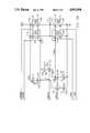
- FIG. 1is a block diagram schematic of a frequency synthesizer suitable for embodying the broad principles of the present invention.
- FIG. 2is a circuit schematic of an alternate embodiment of a storage device suitable for use in the frequency synthesizer depicted in FIG. 1.
- FIG. 3is a logic circuit schematic of an embodiment suitable for use as a control circuit of the frequency synthesizer depicted in FIG. 1.
- FIG. 4depicts timing waveforms A-G which illustrate an operation of the control circuit embodiment depicted in FIG. 3.
- FIGS. 5A-Bdepict, in combination, a circuit schematic embodiment of a charging circuit suitable for use in the frequency synthesizer depicted in FIG. 1.
- phase locked loop 10Shown within dot-dashed lines in FIG. 1, as part of the frequency synthesizer, is a phase locked loop 10.
- the central controller 16may also be used to generate a battery saver signal over signal line 20.
- the reference frequency signal 14is provided to a divide by K prescaler circuit 22 and the resulting signal therefrom is provided over signal line 24 to one input of a phase detector circuit 26.
- Command signals NPU and NPD generated by the detector circuit 26are coupled to a charging circuit 28 which has an output 30 coupled to a storage device 32 which may include a capacitor 34 coupled between the signal line 30 and ground potential.
- a signal representative of the voltage potential across the storage capacitor 34may be coupled to a voltage controlled oscillator 36 utilizing signal line 38.
- the oscillator 36generates a signal, having a frequency commensurate with the voltage potential of signal line 38, over signal line 40 for use by an electronic device such as a radio receiver, for example.
- the frequency signalmay be conducted over signal line 42 to a divide by N circuit 44.
- the output of the divider circuit 44referred to as the feedback frequency signal, is conducted to the phase detector 36 over signal line 46.
- an alternate embodiment of the storage device 32is shown in the schematic of FIG. 2 wherein an active device such as an operational amplifier, for example, is coupled between the capacitive element 34 and oscillator circuit 36.
- the capacitor 34may be coupled to the non-inverting (+) input of an operational amplifier 58 and the inverting (-) input thereof may be coupled to the node of series connected resistors R1 and R2 which are coupled between the output of amplifier 58 and ground.
- the output of operational amplifier 58generates an amplified voltage signal, proportional to the voltage across the capacitor 34.
- the generated voltage signalis conducted to the oscillator 36 over signal line 38 for controlling the frequency of the oscillator generated signal.
- the battery saving signal of line 20may be coupled to the reference oscillator 12, the charging circuit 28, and a switch 48 operative to connect and disconnect a battery supply Vs to the voltage controlled oscillator 36 for energization and enablement thereof.
- the central controller 16may provide from time to time, for programming purposes, 32 bits of information to a memory circuit 50 which distributes the digital information to the prescaler circuit 22, the charging circuit 28, and the divide by N circuit 44. More specifically, 11 bits of data are provided to the prescaler circuit 22 over data lines 52 to set the value of K thereof. In addition, 19 bits of data are conducted to the circuit 44 over data lines 54 to set the value of N in the operation thereof. Further, two bits of data are conducted from the memory 50 to the charging circuit 28 over data lines 56 to set phase loop bandwidth therein.
- the battery saving signal 20may be generated with periodic sleep and awake cycles as exemplified by the waveform A in FIG. 4.
- the sleep cycles of the waveform Aare characterized by the signal going low for duration 60 and the awake cycles are characterized by the signal going high for the duration 62.
- the commencement of the sleep cyclesis shown at the edges 64, and the commencement of the awake cycles is shown at the signal edges 66.
- the oscillators 12 and 36are governed to inhibit the generation of their respective frequency signals which substantially reduces the energy drain on the battery source Vs.
- the output line 30 of the charging circuit 28is governed to a floating state in order to maintain the voltage potential across the storage capacitor 34 for the duration of each sleep cycle.
- the oscillators 12 and 36are enabled to generate their respective frequency signals, and the charging circuit 28 is enabled to adjust the voltage potential across the capacitive element 34 as governed by the phase detector command signals NPU and NPD. More specifically, the phases of the reference and feedback frequency signals are compared by the phase detector 26 which issues current sourcing and current sinking command signals NPU and NPD to the charging circuit 28 to source and sink current over signal line 30 to adjust the voltage across the capacitive element 34.
- a signal representing the adjusted voltageis conducted to the oscillator 36 over signal line 38 to control the frequency of its generated signal which may be conducted over signal line 40 for use as a channel frequency signal in the demodulation section of a radio receiver, for example.
- the channel frequency signalis divided by N in the circuit 44 and the resultant signal is fed back to the phase detector 36 over signal line 46.
- This operationis well known and is characterized as phase locking the feedback frequency signal 46 to the very stable reference frequency signal 24.
- the synthesized frequency of the signal 40becomes the prescaled reference frequency multiplied by the value of N of circuit 44.
- the central controller 16may from time to time provide new values for the prescaler K and the divider N in order to change the frequency of the signal 40 between predetermined channels. Concurrently with the switching of synthesized frequency, the loop bandwidth of the phase locked loop 10 may be altered to a high loop bandwidth setting by the two bits of data 56 provided to the charging circuit 28 which operation provides for a more expeditious phase lock in the dynamics of switching from one synthesized frequency to another. As the loop 10 approaches a phase lock condition, the loop bandwidth may be changed again to a low loop bandwidth setting by the central controller 16 via new data over signal line 18 to the memory 50 which conducts the loop bandwidth governing signals over signal lines 56 to the charging circuit 28. This technique of switching between loop bandwidths will be described in greater herein below.
- the oscillators 12 and 36are not immediately effectively enabled, i.e. they do not immediately begin generating effective or viable frequency signals, but rather require a period of time to settle and stabilize before generating their respective desired frequency signals having positive and negative sloping edges between adequate amplitude levels.
- Present frequency synthesizerspermit the charging circuit 28 to begin sourcing and sinking current to the capacitor 34 as commanded by the phase detector circuit 26 at the commencement 66 of an awake cycle 62.
- the phase detector 26responds by commanding the charging circuit 28 to adjust the voltage of the storage device 32 which controls the oscillator 46.
- the voltage potentialmay be altered substantially away from its desired setting, i.e. the level which was maintained through the sleep cycle, so that phase lock will not be completed at the end of the oscillator start up time but rather will require further time in order to readjust the voltage across the capacitive element 34 back to its desired setting.
- a control circuit 70is included as part of the phase locked loop 10 of the frequency synthesizer.
- the reference frequency signal 24, feedback frequency signal 46, and battery saving signal 20are provided as inputs to the control circuit 70.
- An output control signal from the circuit 70is conducted over signal line 72 to the charging circuit 28 to govern the operation thereof.
- the control circuit 70is governed by the battery saving signal 20, the reference frequency signal 24, and the feedback frequency signal 46 to inhibit the adjustment of the governing voltage potential across the capacitive element 34 by the charging circuit 28 until both of the oscillator circuits 12 and 36 are determined to be effectively enabled in response to an awake cycle of the battery saving signal 20. More specifically, the control circuit 70 tests the reference and feedback frequency signals to determine the initial time in an awake cycle 62 when both such signals are effectively generated by their respective generating means 12 and 36 and to control the charging circuit at such determined initial time to begin adjustment of the governing voltage potential.
- a suitable embodiment for the control circuit 70 of the frequency synthesizeris shown in the circuit schematic diagram of FIG. 3.
- the reference frequency signalis conducted over signal line 24 to the clock input of a D-type flip-flop 74 which has its Q output coupled to one input of a NAND gate 76 over signal line 78.
- the data input D of the flip-flop 74may be coupled to a voltage supply Vs having a sufficient amplitude level to constitute a logical 1.
- the battery saving signalmay be coupled over signal line 20 to one input of the NAND gate 86 and also to an input to an inverter gate 80.
- Another input of NAND gate 86may be coupled to a signal "ON" which may be supplied to the control circuit 70 for the charging circuit 28.
- the feedback frequency signalmay be coupled to the clock input of another D type flip-flop 82 over signal line 46.
- the Q output of flip-flop 82may be coupled to another input of the NAND gate 76 over signal line 84.
- the data input D of flip-flop 82may also be coupled to the voltage potential Vs.
- the output of the NAND gate 76may be coupled to another input of NAND gate 86, the output of which being coupled to reset R inputs of the flip-flops 74 and 82 and also to the clock input of another D type flip-flop 88.
- the data input D and reset input R of the flip-flop 88may be coupled respectively to the supply Vs and the output of the inverter gate 80.
- the Q output of the flip-flop 88becomes the enabling/inhibiting control signal conducted to the charging circuit 28 over signal line 72.
- the oscillators 12 and 36are considered to be effectively enabled within an awake cycle of the battery saving signal when they generate their respective frequency signals having positive and negative sloping edges between adequate amplitude levels.
- the test for determining when both of the oscillators 12 and 36 first become effectively enabledis by determining when a selected one of such sloping edges first occurs in an awake cycle for both of the reference and feedback frequency signals.
- the control circuit 70generates an enabling signal over signal line 72 to the charging circuit 28 to initiate the charging operations thereof. Accordingly, until such time, the adjustment of the governing voltage potential is inhibited and thus such voltage potential is maintained substantially at the desired level throughout the oscillator start up time.
- waveform Bexhibits illustratively the waveform of the reference frequency signal as generated by the reference oscillator 12 governed by the battery saving signal, waveform C the feedback frequency signal, waveform D the Q output of flip-flop 74, waveform E the Q output of flip-flop 82, waveform F the output signal of NAND gate 86, and waveform G the Q output of flip-flop 88 which is the control signal 72.
- the battery saving signal 20disables the NAND gate 86 and causes the flip-flop 88 to be reset through the inverter gate 80.
- the control signal 72goes low to inhibit the charging operations of the circuit 28 as described above.
- the control signal 72is maintained low throughout the sleep cycle 60, and the governing voltage potential across the capacitive element 34 is maintained at the desired level.
- both oscillators 12 and 36are enabled by the battery saving signal and the signal "ON" is set to a logical 1 via charging circuit 28.
- a reference frequency signalis generated with a positive slope effective to clock the D type flip-flop 74 and set its output to a logical one which is shown in the waveform D at 92.
- the feedback frequency signalis generated by the oscillator 36 with a positive sloping edge effective to clock the D type flip-flop 82 and set its Q output to a logical 1 as shown by the waveform E at 96.
- the NAND gate 76responds to the resetting of the Q outputs of the flip-flops 74 and 82 and drives the output of NAND gate 86 to a logical 0 as shown at time 106 in waveform F.
- the transition of the control signal of waveform G from a logical 0 to a logical 1 at time 104causes the circuit 28 to be enabled and commence its charging operations which will be described in greater detail here below in connection with FIGS. 5A and 5B.
- the charging circuit 28may be considered as divided into two parts, one being a logical control circuit and the other being an analog charging circuit.
- FIG. 5Arepresents a suitable embodiment of the logical control section of the charging circuit 28.
- a section of the memory 50 containing two bits of information which are conducted over signal lines to the charging circuit 28is depicted in FIG. 5A for completeness.
- D type flip-flops 110 and 112are included in the memory section 50 to store the two bits of data.
- the control lines 18 coupled from the central controller 16include a serial data path SD for providing serial digital data to the D type flip-flops of the section 50.
- complementary clocking signals SC and NSCare part of the signal lines 18 and used to clock the D type flip-flops of the memory section 50 in order to store the serial digital data provided over line SD.
- a reset signal RSTis provided as part of the control lines to reset the flip-flops of the memory section 50.
- the digital control bits 56are conducted to corresponding D-type latches 114 and 116 of the charging circuit as depicted in FIG. 5A.
- the battery saver signal over signal line 20is coupled to a reset input of each of the latches 114 and 116.
- complementary clocking signals LC and NLCare coupled to the flip-flops 114 and 116 to provide control for the storage of the respective digital bits therein.
- the stored digital data bits of flip-flops 114 and 116will hereinafter be referred to as Q1 and Q2, respectively, and their complements will hereinafter be referred to as Q1 and Q2.
- the command signals NPU and NPDare coupled respectively through inverter gates 118 and 120 to one input of NAND gates 122 and 124, respectively.
- the control signal line 72is coupled to another input of the NAND gates 122 and 124.
- An auto bandwidth signal AUTBWis coupled through an inverter gate 126 to one input of another NAND gate 128.
- Another input of the NAND gate 128is coupled to the signal line of Q2.
- the signal line of Q1is coupled to one input of another NAND gate 130 which has another input thereof coupled to the output of the NAND gate 128.
- the signal lines Q1 and Q2are coupled to two inputs of a NAND gate 132, the output of which effecting a signal ON which is coupled through an inverter gate 134 to effect the complement NON thereof.
- the signal ONis coupled to the control circuit 70 for use therein as described in connection with the embodiment of FIG. 3.
- the output of the NAND gate 124is coupled through an inverter gate 136 to effect a control signal LBW and also coupled to one input of a NOR gate 138.
- the output of the NAND gate 130is coupled to another input of the NOR gate 138 and to an input of another NOR gate 140.
- the output of the NAND gate 122effects a control signal NLBW and is coupled to the other input of the NOR gate 140.
- the output of the NOR gate 140is coupled through an inverter gate 142 to produce another control signal NHBW
- the output of the NOR gate 138is coupled through a pair of cascaded inverter gates 144 and 146 to effect still another control signal HBW.
- the control signals NLBW, NHBW, HBW, and LBWare used in the charging circuit 28 to control MOSFET switches for the sourcing and sinking of current over signal line 30 to the storage capacitor 34.
- MOSFET transistorsare constructed in a circuit arrangement to form current mirrors which set the current levels for low bandwidth and high bandwidth phase locked loop states.
- the numbers shown alongside each of the MOSFET transistorsrepresent their respective width over length ratios.
- the combination of MOSFET transistors 150, 152, 154, and 156are coupled in tandem between the supply VDD and ground to effect a bias current I1 for the diode section 150, 152 of the current mirrors of the current sourcing stages.
- the value of the sourcing bias current I1is set by a bias voltage NBIAS applied to the gate of the transistor 154.
- the value of the bias current I2is set by a bias voltage PBIAS applied to the gate of the transistor 160.
- a voltage Vg1is produced at the drain of the diode configured MOSFET transistor 152 and is coupled to the gates of two MOSFET transistors 166 and 168 to produce a current mirroring effect thereat. That is, the sourcing current conducted through transistor 166 is an amplification of the bias current I1 based on the width to length ratios of the transistors 152 and 166. In the present embodiment, this ratio was set at a value of 8 (low bandwidth state). Similarly, the sourcing current conducted through the transistor 168 is also an amplification of the bias current I1 for the same reasons, and for the present embodiment, the amplification was set at 400 (high bandwidth state).
- a voltage Vg2is effected at the source of the diode configured MOSFET transistor 162 in accordance with the value of the bias current I2.
- the voltage signal Vg2is coupled to the gates of two MOSFET transistors 170 and 172 to produce the current mirroring effects for the sinking currents in both the low bandwidth and high bandwidth states as that described above for the transistors 166 and 168.
- the amplification settings for the transistors 170 and 172are substantially the same as those set for transistors 166 and 168, respectively.
- MOSFET transistors 174 and 176are coupled between the transistors 166 and 168, respectively, and a voltage supply VDD.
- the switches 174 and 176are controlled by the respective signals NLBW and NHBW to conduct and not conduct sourcing current through the transistors 166 and 168, respectively.
- the coupled transistor pair 166 and 174will be referred to as SW1
- the coupled pair of transistors 168 and 176will be referred to as SW2.
- the MOSFET transistors 178 and 180are coupled between their respective transistors 170 and 172 and ground potential.
- the transistors 178 and 180are controlled by the signals LBW and HBW to conduct and not conduct sinking current through their respectively coupled transistors 170 and 172.
- the coupled pairs 170, 178 and 172, 180will be referred to as SW3 and SW4, respectively.
- source currentmay be supplied to or drained from the capacitive element 34 via signal line 30 through SW1 or SW3 as controlled by the signals NLBW and LBW, respectively.
- sourcing currentis supplied through both SW1 and SW2 and sinking current is conducted through SW3 and SW4 as controlled by the signals LBW and HBW, respectively.
- the designis such that when both signals NHBW and NLBW are both logical 1's and signals LBW and HBW are both logical 0, all of the switches SW1, SW2, SW3, and SW4 are off, creating a floating state at the conduction line 30. This floating state is created during the inhibit control stage of the control signal 72 in order to maintain the voltage across the capacitive element 34.
- the NAND gates 122 and 124are disabled effecting a logical 1 at the output thereof.
- the charging circuit 28is inhibited from adjusting the voltage across the capacitive element 34 which state continues for the duration of the inhibit cycle of the control signal 72.
- the control signalis changed to a logical 1 representative of the commencement of an enable cycle of the control signal 72 which change in state enables the NAND gates 122 and 124 to thereafter respond to their respective command signals NPU and NPD (see FIG. 5A).
Landscapes
- Stabilization Of Oscillater, Synchronisation, Frequency Synthesizers (AREA)
Abstract
Description
__________________________________________________________________________TRUTH TABLE A 01 02 NPU NPD LBW HBW NLBW NHBW SW1 SW2 SW3 SW4 __________________________________________________________________________X 1 0 1 0 1 1 1 l OFF OFF ON ON X 0 X 1 0 1 0 1 1 OFF OFF ON OFF 1 1 1 1 0 1 1 1 1 OFFOFF ON ON 0 1 1 1 0 1 0 1 1 OFF OFF ON OFF X 1 0 0 1 0 0 0 0 ON ON OFF OFF X 0X 0 1 0 0 0 l ON OFF OFF OFF 1 1 1 0l 0 0 0 0 ON ON OFF OFF 0 l 1 0 1 0 0 0 1 ON OFF OFF OFF __________________________________________________________________________
Claims (8)
Priority Applications (6)
| Application Number | Priority Date | Filing Date | Title |
|---|---|---|---|
| US07/322,393US4893094A (en) | 1989-03-13 | 1989-03-13 | Frequency synthesizer with control of start-up battery saving operations |
| JP2505441AJPH04505840A (en) | 1989-03-13 | 1990-02-23 | Frequency synthesizer with startup battery saving operation control function |
| PCT/US1990/000896WO1990010978A1 (en) | 1989-03-13 | 1990-02-23 | Frequency synthesizer with control of start-up battery saving operations |
| EP19900905808EP0464139A4 (en) | 1989-03-13 | 1990-02-23 | Frequency synthesizer with control of start-up battery saving operations |
| CA002046294ACA2046294A1 (en) | 1989-03-13 | 1990-02-23 | Frequency synthesizer with control of start-up battery saving operations |
| KR1019900702431AKR920700495A (en) | 1989-03-13 | 1990-02-23 | Frequency synthesizer |
Applications Claiming Priority (1)
| Application Number | Priority Date | Filing Date | Title |
|---|---|---|---|
| US07/322,393US4893094A (en) | 1989-03-13 | 1989-03-13 | Frequency synthesizer with control of start-up battery saving operations |
Publications (1)
| Publication Number | Publication Date |
|---|---|
| US4893094Atrue US4893094A (en) | 1990-01-09 |
Family
ID=23254693
Family Applications (1)
| Application Number | Title | Priority Date | Filing Date |
|---|---|---|---|
| US07/322,393Expired - LifetimeUS4893094A (en) | 1989-03-13 | 1989-03-13 | Frequency synthesizer with control of start-up battery saving operations |
Country Status (6)
| Country | Link |
|---|---|
| US (1) | US4893094A (en) |
| EP (1) | EP0464139A4 (en) |
| JP (1) | JPH04505840A (en) |
| KR (1) | KR920700495A (en) |
| CA (1) | CA2046294A1 (en) |
| WO (1) | WO1990010978A1 (en) |
Cited By (49)
| Publication number | Priority date | Publication date | Assignee | Title |
|---|---|---|---|---|
| WO1991002413A1 (en)* | 1989-08-01 | 1991-02-21 | At&E Corporation | Radio receiver frequency control system |
| US5059925A (en)* | 1990-09-28 | 1991-10-22 | Stratacom, Inc. | Method and apparatus for transparently switching clock sources |
| US5103192A (en)* | 1989-06-14 | 1992-04-07 | Fujitsu Limited | Phase-difference detecting circuit and method of reducing power consumption in a pll system |
| US5125107A (en)* | 1989-03-02 | 1992-06-23 | Motorola, Inc. | Diagnostic mode for a frequency synthesizer |
| US5128632A (en)* | 1991-05-16 | 1992-07-07 | Motorola, Inc. | Adaptive lock time controller for a frequency synthesizer and method therefor |
| US5160900A (en)* | 1992-01-21 | 1992-11-03 | Nokia Mobile Phones Ltd. | Method to speed up the training of a shift oscillator in a frequency synthesizer |
| US5163159A (en)* | 1990-07-30 | 1992-11-10 | Motorola, Inc. | Dual mode automatic frequency control |
| US5223755A (en)* | 1990-12-26 | 1993-06-29 | Xerox Corporation | Extended frequency range variable delay locked loop for clock synchronization |
| US5256980A (en)* | 1991-07-09 | 1993-10-26 | Pairgain Technologies, Inc. | Frequency synthesizer incorporating vernier phase adjuster |
| US5257294A (en)* | 1990-11-13 | 1993-10-26 | National Semiconductor Corporation | Phase-locked loop circuit and method |
| US5335365A (en)* | 1991-07-08 | 1994-08-02 | Motorola, Inc. | Frequency synthesizer with VCO output control |
| US5349310A (en)* | 1993-06-09 | 1994-09-20 | Alcatel Network Systems, Inc. | Digitally controlled fractional frequency synthesizer |
| WO1995004405A1 (en)* | 1993-07-30 | 1995-02-09 | Apple Computer, Inc. | Method and apparatus for charge pump with reduced charge injection |
| US5420545A (en)* | 1993-03-10 | 1995-05-30 | National Semiconductor Corporation | Phase lock loop with selectable frequency switching time |
| US5440595A (en)* | 1992-12-07 | 1995-08-08 | Nec Corporation | Communication apparatus with low power consumption |
| WO1995022206A1 (en)* | 1994-02-15 | 1995-08-17 | Rambus, Inc. | Delay-locked loop |
| US5475877A (en)* | 1993-03-26 | 1995-12-12 | Mitsubishi Denki Kabushiki Kaisha | Mobile wireless set with improved intermittent operation control and reduced power consumption |
| US5483687A (en)* | 1993-11-10 | 1996-01-09 | Motorola, Inc. | Operational transconductance amplifier track and hold system |
| US5488332A (en)* | 1994-06-10 | 1996-01-30 | Oki Telecom | Reversed phase-locked loop |
| US5491439A (en)* | 1994-08-31 | 1996-02-13 | International Business Machines Corporation | Method and apparatus for reducing jitter in a phase locked loop circuit |
| US5495207A (en)* | 1994-08-31 | 1996-02-27 | International Business Machines Corporation | Differential current controlled oscillator with variable load |
| US5513225A (en)* | 1994-08-31 | 1996-04-30 | International Business Machines Corporation | Resistorless phase locked loop circuit employing direct current injection |
| US5525932A (en)* | 1994-08-31 | 1996-06-11 | International Business Machines Corporation | Lock indicator for phase locked loop circuit |
| US5541929A (en)* | 1992-04-10 | 1996-07-30 | Nec Corporation | TDMA mobile unit frequency synthesizer having power saving mode during transmit and receive slots |
| US5594735A (en)* | 1992-04-10 | 1997-01-14 | Nec Corporation | TDMA mobile unit frequency synthesizer having power saving mode during transmit and receive slots |
| US5613235A (en)* | 1995-06-29 | 1997-03-18 | Nokia Mobile Phones Limited | Operation of a radiotelephone in a synchronous extended standby mode for conserving battery power |
| US5617062A (en)* | 1995-06-07 | 1997-04-01 | American Microsystems, Inc. | Timing circuit with rapid initialization on power-up |
| US5619161A (en)* | 1994-08-31 | 1997-04-08 | International Business Machines Corporation | Diffrential charge pump with integrated common mode control |
| DE4498746T1 (en)* | 1993-11-09 | 1997-07-31 | Motorola Inc | Device and method for releasing elements of a phase-locked loop |
| US5708687A (en)* | 1993-06-09 | 1998-01-13 | Alcatel Network Systems, Inc. | Synchronized clock using a non-pullable reference oscillator |
| US5736892A (en)* | 1993-12-10 | 1998-04-07 | Rambus, Inc. | Differential charge pump circuit with high differential impedance and low common mode impedance |
| WO1998021827A1 (en)* | 1996-11-15 | 1998-05-22 | Analog Devices | Low power charge pump |
| US5808498A (en)* | 1995-05-26 | 1998-09-15 | Rambus, Inc. | At frequency phase shifting circuit for use in a quadrature clock generator |
| US5825209A (en)* | 1997-02-27 | 1998-10-20 | Rambus Inc. | Quadrature phase detector |
| US6072250A (en)* | 1998-06-01 | 2000-06-06 | Motorola, Inc. | Battery pack having a hibernate circuit |
| US6097933A (en)* | 1997-12-04 | 2000-08-01 | Glenayre Electronics, Inc. | Method and apparatus for conserving power in a pager |
| US6104915A (en)* | 1997-10-09 | 2000-08-15 | Nortel Networks Corporation | Synchronization system using aging prediction |
| US6157821A (en)* | 1997-10-23 | 2000-12-05 | Ericsson Inc. | Voltage step up for a low voltage frequency synthesizer architecture |
| US6160490A (en)* | 1998-02-02 | 2000-12-12 | Motorola | Apparatus for improving the battery life of a selective call receiver |
| US6340900B1 (en) | 1994-02-15 | 2002-01-22 | Rambus, Inc. | Phase detector with minimized phase detection error |
| US6356538B1 (en) | 1998-03-30 | 2002-03-12 | Oki Telecom, Inc. | Partial sleep system for power savings in CDMA wireless telephone devices |
| US20020077074A1 (en)* | 2000-10-10 | 2002-06-20 | Francesco Piazza | RF receiver with power off control |
| US6642746B2 (en) | 1996-01-02 | 2003-11-04 | Rambus Inc. | Phase detector with minimized phase detection error |
| US20030220087A1 (en)* | 2002-05-27 | 2003-11-27 | Nokia Corporation | Circuit arrangement for phase locked loop, and phase locked loop based method to be used in cellular network terminals |
| US6728521B1 (en)* | 1999-05-28 | 2004-04-27 | Stmicroelectronics, S.A. | Phase locked device with reduced electrical consumption |
| US20050253734A1 (en)* | 2004-05-13 | 2005-11-17 | Matsushita Electric Industrial Co., Ltd. | Communication device |
| EP1612944A1 (en)* | 2004-07-01 | 2006-01-04 | Krohne Messtechnik Gmbh & Co. Kg | Frequency synthesizer and method of operating a frequency synthesizer |
| US7027796B1 (en)* | 2001-06-22 | 2006-04-11 | Rfmd Wpan, Inc. | Method and apparatus for automatic fast locking power conserving synthesizer |
| US20190165792A1 (en)* | 2017-11-27 | 2019-05-30 | Anapass Inc. | Phase-locked loop and delay-locked loop |
Families Citing this family (2)
| Publication number | Priority date | Publication date | Assignee | Title |
|---|---|---|---|---|
| US5683668A (en)* | 1990-09-20 | 1997-11-04 | The United States Of America As Represented By The Department Of Health And Human Services | Method of generating nitric oxide gas using nitric oxide complexes |
| FI87033C (en)* | 1990-10-05 | 1992-11-10 | Nokia Mobile Phones Ltd | Method for arranging switching type controls in a radio telephone |
Citations (3)
| Publication number | Priority date | Publication date | Assignee | Title |
|---|---|---|---|---|
| US4631496A (en)* | 1981-04-06 | 1986-12-23 | Motorola, Inc. | Battery saving system for a frequency synthesizer |
| US4673892A (en)* | 1985-05-13 | 1987-06-16 | Nec Corporation | Phase locked loop frequency synthesizer with battery saving circuit |
| US4743864A (en)* | 1985-10-23 | 1988-05-10 | Hitachi, Ltd | Power saving intermittently operated phase locked loop |
Family Cites Families (2)
| Publication number | Priority date | Publication date | Assignee | Title |
|---|---|---|---|---|
| US4745372A (en)* | 1985-10-17 | 1988-05-17 | Matsushita Electric Industrial Co., Ltd. | Phase-locked-loop circuit having a charge pump |
| CA1290407C (en)* | 1986-12-23 | 1991-10-08 | Shigeki Saito | Frequency synthesizer |
- 1989
- 1989-03-13USUS07/322,393patent/US4893094A/ennot_activeExpired - Lifetime
- 1990
- 1990-02-23WOPCT/US1990/000896patent/WO1990010978A1/ennot_activeApplication Discontinuation
- 1990-02-23CACA002046294Apatent/CA2046294A1/ennot_activeAbandoned
- 1990-02-23JPJP2505441Apatent/JPH04505840A/enactivePending
- 1990-02-23KRKR1019900702431Apatent/KR920700495A/ennot_activeCeased
- 1990-02-23EPEP19900905808patent/EP0464139A4/ennot_activeWithdrawn
Patent Citations (3)
| Publication number | Priority date | Publication date | Assignee | Title |
|---|---|---|---|---|
| US4631496A (en)* | 1981-04-06 | 1986-12-23 | Motorola, Inc. | Battery saving system for a frequency synthesizer |
| US4673892A (en)* | 1985-05-13 | 1987-06-16 | Nec Corporation | Phase locked loop frequency synthesizer with battery saving circuit |
| US4743864A (en)* | 1985-10-23 | 1988-05-10 | Hitachi, Ltd | Power saving intermittently operated phase locked loop |
Cited By (67)
| Publication number | Priority date | Publication date | Assignee | Title |
|---|---|---|---|---|
| US5125107A (en)* | 1989-03-02 | 1992-06-23 | Motorola, Inc. | Diagnostic mode for a frequency synthesizer |
| US5103192A (en)* | 1989-06-14 | 1992-04-07 | Fujitsu Limited | Phase-difference detecting circuit and method of reducing power consumption in a pll system |
| WO1991002413A1 (en)* | 1989-08-01 | 1991-02-21 | At&E Corporation | Radio receiver frequency control system |
| DE4191766C2 (en)* | 1990-07-30 | 1999-08-19 | Motorola Inc | Frequency control circuit for an adjustable receiver oscillator |
| US5163159A (en)* | 1990-07-30 | 1992-11-10 | Motorola, Inc. | Dual mode automatic frequency control |
| DE4191766T1 (en)* | 1990-07-30 | 1997-07-31 | Motorola Inc | Automatic dual mode frequency control |
| US5059925A (en)* | 1990-09-28 | 1991-10-22 | Stratacom, Inc. | Method and apparatus for transparently switching clock sources |
| US5257294A (en)* | 1990-11-13 | 1993-10-26 | National Semiconductor Corporation | Phase-locked loop circuit and method |
| US5223755A (en)* | 1990-12-26 | 1993-06-29 | Xerox Corporation | Extended frequency range variable delay locked loop for clock synchronization |
| US5128632A (en)* | 1991-05-16 | 1992-07-07 | Motorola, Inc. | Adaptive lock time controller for a frequency synthesizer and method therefor |
| US5335365A (en)* | 1991-07-08 | 1994-08-02 | Motorola, Inc. | Frequency synthesizer with VCO output control |
| US5256980A (en)* | 1991-07-09 | 1993-10-26 | Pairgain Technologies, Inc. | Frequency synthesizer incorporating vernier phase adjuster |
| US5160900A (en)* | 1992-01-21 | 1992-11-03 | Nokia Mobile Phones Ltd. | Method to speed up the training of a shift oscillator in a frequency synthesizer |
| US5541929A (en)* | 1992-04-10 | 1996-07-30 | Nec Corporation | TDMA mobile unit frequency synthesizer having power saving mode during transmit and receive slots |
| US5594735A (en)* | 1992-04-10 | 1997-01-14 | Nec Corporation | TDMA mobile unit frequency synthesizer having power saving mode during transmit and receive slots |
| US5440595A (en)* | 1992-12-07 | 1995-08-08 | Nec Corporation | Communication apparatus with low power consumption |
| US5420545A (en)* | 1993-03-10 | 1995-05-30 | National Semiconductor Corporation | Phase lock loop with selectable frequency switching time |
| US5475877A (en)* | 1993-03-26 | 1995-12-12 | Mitsubishi Denki Kabushiki Kaisha | Mobile wireless set with improved intermittent operation control and reduced power consumption |
| US5790614A (en)* | 1993-06-09 | 1998-08-04 | Alcatel Network Systems, Inc. | Synchronized clock using a non-pullable reference oscillator |
| US5708687A (en)* | 1993-06-09 | 1998-01-13 | Alcatel Network Systems, Inc. | Synchronized clock using a non-pullable reference oscillator |
| US5349310A (en)* | 1993-06-09 | 1994-09-20 | Alcatel Network Systems, Inc. | Digitally controlled fractional frequency synthesizer |
| WO1995004405A1 (en)* | 1993-07-30 | 1995-02-09 | Apple Computer, Inc. | Method and apparatus for charge pump with reduced charge injection |
| US6185411B1 (en)* | 1993-11-09 | 2001-02-06 | Motorola Inc. | Apparatus and method for enabling elements of a phase locked loop |
| DE4498746T1 (en)* | 1993-11-09 | 1997-07-31 | Motorola Inc | Device and method for releasing elements of a phase-locked loop |
| US5483687A (en)* | 1993-11-10 | 1996-01-09 | Motorola, Inc. | Operational transconductance amplifier track and hold system |
| US5736892A (en)* | 1993-12-10 | 1998-04-07 | Rambus, Inc. | Differential charge pump circuit with high differential impedance and low common mode impedance |
| USRE36013E (en)* | 1993-12-10 | 1998-12-29 | Rambus, Inc. | Differential charge pump circuit with high differential and low common mode impedance |
| WO1995022206A1 (en)* | 1994-02-15 | 1995-08-17 | Rambus, Inc. | Delay-locked loop |
| US5614855A (en)* | 1994-02-15 | 1997-03-25 | Rambus, Inc. | Delay-locked loop |
| US6340900B1 (en) | 1994-02-15 | 2002-01-22 | Rambus, Inc. | Phase detector with minimized phase detection error |
| US6480035B1 (en) | 1994-02-15 | 2002-11-12 | Rambus, Inc. | Phase detector with minimized phase detection error |
| US5488332A (en)* | 1994-06-10 | 1996-01-30 | Oki Telecom | Reversed phase-locked loop |
| US5525932A (en)* | 1994-08-31 | 1996-06-11 | International Business Machines Corporation | Lock indicator for phase locked loop circuit |
| US5495207A (en)* | 1994-08-31 | 1996-02-27 | International Business Machines Corporation | Differential current controlled oscillator with variable load |
| US5491439A (en)* | 1994-08-31 | 1996-02-13 | International Business Machines Corporation | Method and apparatus for reducing jitter in a phase locked loop circuit |
| US5513225A (en)* | 1994-08-31 | 1996-04-30 | International Business Machines Corporation | Resistorless phase locked loop circuit employing direct current injection |
| US5546052A (en)* | 1994-08-31 | 1996-08-13 | International Business Machines Corporation | Phase locked loop circuit with phase/frequency detector which eliminates dead zones |
| US5619161A (en)* | 1994-08-31 | 1997-04-08 | International Business Machines Corporation | Diffrential charge pump with integrated common mode control |
| US5808498A (en)* | 1995-05-26 | 1998-09-15 | Rambus, Inc. | At frequency phase shifting circuit for use in a quadrature clock generator |
| USRE37452E1 (en) | 1995-05-26 | 2001-11-20 | Rambus Inc. | At frequency phase shifting circuit for use in a quadrature clock generator |
| US5617062A (en)* | 1995-06-07 | 1997-04-01 | American Microsystems, Inc. | Timing circuit with rapid initialization on power-up |
| US5613235A (en)* | 1995-06-29 | 1997-03-18 | Nokia Mobile Phones Limited | Operation of a radiotelephone in a synchronous extended standby mode for conserving battery power |
| US6642746B2 (en) | 1996-01-02 | 2003-11-04 | Rambus Inc. | Phase detector with minimized phase detection error |
| WO1998021827A1 (en)* | 1996-11-15 | 1998-05-22 | Analog Devices | Low power charge pump |
| US5847614A (en)* | 1996-11-15 | 1998-12-08 | Analog Devices, Inc. | Low power charge pump |
| US5825209A (en)* | 1997-02-27 | 1998-10-20 | Rambus Inc. | Quadrature phase detector |
| US6104915A (en)* | 1997-10-09 | 2000-08-15 | Nortel Networks Corporation | Synchronization system using aging prediction |
| US6157821A (en)* | 1997-10-23 | 2000-12-05 | Ericsson Inc. | Voltage step up for a low voltage frequency synthesizer architecture |
| US6097933A (en)* | 1997-12-04 | 2000-08-01 | Glenayre Electronics, Inc. | Method and apparatus for conserving power in a pager |
| US6160490A (en)* | 1998-02-02 | 2000-12-12 | Motorola | Apparatus for improving the battery life of a selective call receiver |
| US6356538B1 (en) | 1998-03-30 | 2002-03-12 | Oki Telecom, Inc. | Partial sleep system for power savings in CDMA wireless telephone devices |
| US6072250A (en)* | 1998-06-01 | 2000-06-06 | Motorola, Inc. | Battery pack having a hibernate circuit |
| US6728521B1 (en)* | 1999-05-28 | 2004-04-27 | Stmicroelectronics, S.A. | Phase locked device with reduced electrical consumption |
| US6968220B2 (en)* | 2000-10-10 | 2005-11-22 | Nemerix Sa | RF receiver with power off control |
| US20020077074A1 (en)* | 2000-10-10 | 2002-06-20 | Francesco Piazza | RF receiver with power off control |
| US7027796B1 (en)* | 2001-06-22 | 2006-04-11 | Rfmd Wpan, Inc. | Method and apparatus for automatic fast locking power conserving synthesizer |
| US20030220087A1 (en)* | 2002-05-27 | 2003-11-27 | Nokia Corporation | Circuit arrangement for phase locked loop, and phase locked loop based method to be used in cellular network terminals |
| US7283801B2 (en)* | 2002-05-27 | 2007-10-16 | Nokia Corporation | Circuit arrangement for phase locked loop, and phase locked loop based method to be used in cellular network terminals |
| US20050253734A1 (en)* | 2004-05-13 | 2005-11-17 | Matsushita Electric Industrial Co., Ltd. | Communication device |
| EP1612945A1 (en)* | 2004-07-01 | 2006-01-04 | Krohne Messtechnik Gmbh & Co. Kg | Frequency synthesizer and method of operating a frequency synthesizer |
| US20060006952A1 (en)* | 2004-07-01 | 2006-01-12 | Thomas Musch | Frequency synthesizer and method for operating a frequency synthesizer |
| EP1612944A1 (en)* | 2004-07-01 | 2006-01-04 | Krohne Messtechnik Gmbh & Co. Kg | Frequency synthesizer and method of operating a frequency synthesizer |
| US20190165792A1 (en)* | 2017-11-27 | 2019-05-30 | Anapass Inc. | Phase-locked loop and delay-locked loop |
| CN109842413A (en)* | 2017-11-27 | 2019-06-04 | 安纳帕斯股份有限公司 | Phaselocked loop and delay lock loop |
| US10516400B2 (en)* | 2017-11-27 | 2019-12-24 | Anapass Inc. | Phase-locked loop and delay-locked loop |
| US10944405B2 (en)* | 2017-11-27 | 2021-03-09 | Anapass Inc. | Phase-locked loop and delay-locked loop |
| CN109842413B (en)* | 2017-11-27 | 2023-08-22 | 安纳帕斯股份有限公司 | Phase-locked loop and delay-locked loop |
Also Published As
| Publication number | Publication date |
|---|---|
| WO1990010978A1 (en) | 1990-09-20 |
| EP0464139A4 (en) | 1992-05-13 |
| JPH04505840A (en) | 1992-10-08 |
| KR920700495A (en) | 1992-02-19 |
| EP0464139A1 (en) | 1992-01-08 |
| CA2046294A1 (en) | 1990-09-14 |
Similar Documents
| Publication | Publication Date | Title |
|---|---|---|
| US4893094A (en) | Frequency synthesizer with control of start-up battery saving operations | |
| US4926141A (en) | Frequency synthesizer with improved automatic control of loop bandwidth selection | |
| US5831483A (en) | PLL frequency synthesizer having circuit for controlling gain of charge pump circuit | |
| US5847614A (en) | Low power charge pump | |
| EP0777333B1 (en) | Power saving PLL circuit | |
| KR100337998B1 (en) | Phase locked loop circuit | |
| JP3250540B2 (en) | PLL circuit | |
| KR100719693B1 (en) | A PLL that operates stably and stably to PVT changes and its operation method | |
| US5955928A (en) | Automatically adjusting the dynamic range of the VCO in a PLL at start-up for optimal operating point | |
| JPH06112815A (en) | Charging pump in phase-locked loop | |
| JP3331115B2 (en) | Frequency phase locked loop | |
| JPH1065530A (en) | Charge pump circuit and pll circuit using it | |
| US4901033A (en) | Frequency synthesizer with dynamically programmable frequency range of selected loop bandwith | |
| USRE36874E (en) | Supply voltage tolerant phase-locked loop circuit | |
| US7446595B2 (en) | Charge pump circuit with power management | |
| JP3609658B2 (en) | PLL circuit | |
| JP3561035B2 (en) | Synchronous clock generation circuit | |
| GB2258960A (en) | Power saving frequency synthesiser with fast pull-in feature | |
| JP4038030B2 (en) | Phase constrained loop | |
| KR100282124B1 (en) | Digital phase-locked loop circuit | |
| US5936473A (en) | Clock generator in which external oscillator is disabled after internal PLL becomes locked | |
| US6304147B1 (en) | Method and circuit for reduced power consumption in a charge pump circuit | |
| JP4066500B2 (en) | PLL circuit | |
| JP2006211376A (en) | Pll circuit and its program | |
| JP3070076B2 (en) | Phase-locked oscillation circuit |
Legal Events
| Date | Code | Title | Description |
|---|---|---|---|
| AS | Assignment | Owner name:MOTOROLA, INC., A DE CORP., ILLINOIS Free format text:ASSIGNMENT OF ASSIGNORS INTEREST.;ASSIGNORS:HEROLD, BARRY W.;TAHERNIA, OMID;REEL/FRAME:005054/0190 Effective date:19890307 | |
| STCF | Information on status: patent grant | Free format text:PATENTED CASE | |
| FEPP | Fee payment procedure | Free format text:PAYOR NUMBER ASSIGNED (ORIGINAL EVENT CODE: ASPN); ENTITY STATUS OF PATENT OWNER: LARGE ENTITY | |
| FPAY | Fee payment | Year of fee payment:4 | |
| FPAY | Fee payment | Year of fee payment:8 | |
| FPAY | Fee payment | Year of fee payment:12 | |
| AS | Assignment | Owner name:FREESCALE SEMICONDUCTOR, INC., TEXAS Free format text:ASSIGNMENT OF ASSIGNORS INTEREST;ASSIGNOR:MOTOROLA, INC.;REEL/FRAME:015698/0657 Effective date:20040404 Owner name:FREESCALE SEMICONDUCTOR, INC.,TEXAS Free format text:ASSIGNMENT OF ASSIGNORS INTEREST;ASSIGNOR:MOTOROLA, INC.;REEL/FRAME:015698/0657 Effective date:20040404 | |
| AS | Assignment | Owner name:CITIBANK, N.A. AS COLLATERAL AGENT, NEW YORK Free format text:SECURITY AGREEMENT;ASSIGNORS:FREESCALE SEMICONDUCTOR, INC.;FREESCALE ACQUISITION CORPORATION;FREESCALE ACQUISITION HOLDINGS CORP.;AND OTHERS;REEL/FRAME:018855/0129 Effective date:20061201 Owner name:CITIBANK, N.A. AS COLLATERAL AGENT,NEW YORK Free format text:SECURITY AGREEMENT;ASSIGNORS:FREESCALE SEMICONDUCTOR, INC.;FREESCALE ACQUISITION CORPORATION;FREESCALE ACQUISITION HOLDINGS CORP.;AND OTHERS;REEL/FRAME:018855/0129 Effective date:20061201 | |
| AS | Assignment | Owner name:FREESCALE SEMICONDUCTOR, INC., TEXAS Free format text:PATENT RELEASE;ASSIGNOR:CITIBANK, N.A., AS COLLATERAL AGENT;REEL/FRAME:037354/0225 Effective date:20151207 |