US4892392A - Picture display cell and method of forming an orientation layer on a substrate of the picture display cell - Google Patents
Picture display cell and method of forming an orientation layer on a substrate of the picture display cellDownload PDFInfo
- Publication number
- US4892392A US4892392AUS07/267,694US26769488AUS4892392AUS 4892392 AUS4892392 AUS 4892392AUS 26769488 AUS26769488 AUS 26769488AUS 4892392 AUS4892392 AUS 4892392A
- Authority
- US
- United States
- Prior art keywords
- display cell
- picture display
- substrate
- monomer
- orientation layer
- Prior art date
- Legal status (The legal status is an assumption and is not a legal conclusion. Google has not performed a legal analysis and makes no representation as to the accuracy of the status listed.)
- Expired - Lifetime
Links
- 239000000758substrateSubstances0.000titleclaimsabstractdescription31
- 238000000034methodMethods0.000titleclaimsabstractdescription18
- 239000000178monomerSubstances0.000claimsabstractdescription47
- 239000007788liquidSubstances0.000claimsabstractdescription24
- 239000002178crystalline materialSubstances0.000claimsabstractdescription8
- 238000007789sealingMethods0.000claimsabstractdescription4
- 238000006116polymerization reactionMethods0.000claimsdescription14
- NIXOWILDQLNWCW-UHFFFAOYSA-MAcrylateChemical compound[O-]C(=O)C=CNIXOWILDQLNWCW-UHFFFAOYSA-M0.000claimsdescription10
- 239000000463materialSubstances0.000claimsdescription10
- 229920000642polymerPolymers0.000claimsdescription9
- 239000003999initiatorSubstances0.000claimsdescription4
- 239000000203mixtureSubstances0.000claimsdescription4
- 125000003118aryl groupChemical group0.000claimsdescription3
- 230000005684electric fieldEffects0.000claimsdescription3
- 125000000217alkyl groupChemical group0.000claimsdescription2
- 125000004093cyano groupChemical group*C#N0.000claimsdescription2
- 239000007767bonding agentSubstances0.000claims1
- 125000004435hydrogen atomChemical group[H]*0.000claims1
- 125000002496methyl groupChemical group[H]C([H])([H])*0.000claims1
- 150000003384small moleculesChemical class0.000claims1
- 150000001875compoundsChemical class0.000abstractdescription6
- 239000010410layerSubstances0.000description25
- 238000006243chemical reactionMethods0.000description7
- 230000007704transitionEffects0.000description6
- 239000010408filmSubstances0.000description5
- 239000004990Smectic liquid crystalSubstances0.000description4
- 239000013047polymeric layerSubstances0.000description4
- HEMHJVSKTPXQMS-UHFFFAOYSA-MSodium hydroxideChemical compound[OH-].[Na+]HEMHJVSKTPXQMS-UHFFFAOYSA-M0.000description3
- 230000001419dependent effectEffects0.000description3
- 239000004973liquid crystal related substanceSubstances0.000description3
- 239000002245particleSubstances0.000description3
- 229910017344Fe2 O3Inorganic materials0.000description2
- 239000004988Nematic liquid crystalSubstances0.000description2
- VYPSYNLAJGMNEJ-UHFFFAOYSA-NSilicium dioxideChemical compoundO=[Si]=OVYPSYNLAJGMNEJ-UHFFFAOYSA-N0.000description2
- 150000001412aminesChemical class0.000description2
- 125000003277amino groupChemical group0.000description2
- RWCCWEUUXYIKHB-UHFFFAOYSA-NbenzophenoneChemical groupC=1C=CC=CC=1C(=O)C1=CC=CC=C1RWCCWEUUXYIKHB-UHFFFAOYSA-N0.000description2
- 238000000151depositionMethods0.000description2
- 125000004386diacrylate groupChemical group0.000description2
- 239000011521glassSubstances0.000description2
- 238000010438heat treatmentMethods0.000description2
- 239000006249magnetic particleSubstances0.000description2
- 229920000620organic polymerPolymers0.000description2
- 230000005855radiationEffects0.000description2
- 229910052814silicon oxideInorganic materials0.000description2
- 238000009987spinningMethods0.000description2
- XOLBLPGZBRYERU-UHFFFAOYSA-Ntin dioxideChemical compoundO=[Sn]=OXOLBLPGZBRYERU-UHFFFAOYSA-N0.000description2
- KWVGIHKZDCUPEU-UHFFFAOYSA-N2,2-dimethoxy-2-phenylacetophenoneChemical compoundC=1C=CC=CC=1C(OC)(OC)C(=O)C1=CC=CC=C1KWVGIHKZDCUPEU-UHFFFAOYSA-N0.000description1
- 239000004593EpoxySubstances0.000description1
- BLRPTPMANUNPDV-UHFFFAOYSA-NSilaneChemical group[SiH4]BLRPTPMANUNPDV-UHFFFAOYSA-N0.000description1
- WYURNTSHIVDZCO-UHFFFAOYSA-NTetrahydrofuranChemical compoundC1CCOC1WYURNTSHIVDZCO-UHFFFAOYSA-N0.000description1
- ZMANZCXQSJIPKH-UHFFFAOYSA-NTriethylamineChemical compoundCCN(CC)CCZMANZCXQSJIPKH-UHFFFAOYSA-N0.000description1
- 239000000853adhesiveSubstances0.000description1
- 230000001070adhesive effectEffects0.000description1
- 125000002947alkylene groupChemical group0.000description1
- QVGXLLKOCUKJST-UHFFFAOYSA-Natomic oxygenChemical compound[O]QVGXLLKOCUKJST-UHFFFAOYSA-N0.000description1
- 239000011230binding agentSubstances0.000description1
- 238000001311chemical methods and processMethods0.000description1
- 238000001816coolingMethods0.000description1
- 230000008021depositionEffects0.000description1
- 230000000694effectsEffects0.000description1
- 238000005516engineering processMethods0.000description1
- 150000002170ethersChemical class0.000description1
- 239000008240homogeneous mixtureSubstances0.000description1
- 229930195733hydrocarbonNatural products0.000description1
- 150000002430hydrocarbonsChemical class0.000description1
- 150000003949imidesChemical class0.000description1
- 238000011065in-situ storageMethods0.000description1
- 150000002576ketonesChemical class0.000description1
- 238000005259measurementMethods0.000description1
- MYWUZJCMWCOHBA-VIFPVBQESA-NmethamphetamineChemical compoundCN[C@@H](C)CC1=CC=CC=C1MYWUZJCMWCOHBA-VIFPVBQESA-N0.000description1
- 230000004048modificationEffects0.000description1
- 238000012986modificationMethods0.000description1
- OKDQKPLMQBXTNH-UHFFFAOYSA-Nn,n-dimethyl-2h-pyridin-1-amineChemical compoundCN(C)N1CC=CC=C1OKDQKPLMQBXTNH-UHFFFAOYSA-N0.000description1
- 230000003287optical effectEffects0.000description1
- 239000003960organic solventSubstances0.000description1
- 229910052760oxygenInorganic materials0.000description1
- 239000001301oxygenSubstances0.000description1
- 230000035699permeabilityEffects0.000description1
- 125000002294quinazolinyl groupChemical groupN1=C(N=CC2=CC=CC=C12)*0.000description1
- SCPYDCQAZCOKTP-UHFFFAOYSA-NsilanolChemical compound[SiH3]OSCPYDCQAZCOKTP-UHFFFAOYSA-N0.000description1
- 239000007787solidSubstances0.000description1
- 239000002904solventSubstances0.000description1
- 239000000126substanceSubstances0.000description1
- 239000010409thin filmSubstances0.000description1
Images


Classifications
- G—PHYSICS
- G03—PHOTOGRAPHY; CINEMATOGRAPHY; ANALOGOUS TECHNIQUES USING WAVES OTHER THAN OPTICAL WAVES; ELECTROGRAPHY; HOLOGRAPHY
- G03F—PHOTOMECHANICAL PRODUCTION OF TEXTURED OR PATTERNED SURFACES, e.g. FOR PRINTING, FOR PROCESSING OF SEMICONDUCTOR DEVICES; MATERIALS THEREFOR; ORIGINALS THEREFOR; APPARATUS SPECIALLY ADAPTED THEREFOR
- G03F7/00—Photomechanical, e.g. photolithographic, production of textured or patterned surfaces, e.g. printing surfaces; Materials therefor, e.g. comprising photoresists; Apparatus specially adapted therefor
- G03F7/004—Photosensitive materials
- G03F7/027—Non-macromolecular photopolymerisable compounds having carbon-to-carbon double bonds, e.g. ethylenic compounds
- C—CHEMISTRY; METALLURGY
- C09—DYES; PAINTS; POLISHES; NATURAL RESINS; ADHESIVES; COMPOSITIONS NOT OTHERWISE PROVIDED FOR; APPLICATIONS OF MATERIALS NOT OTHERWISE PROVIDED FOR
- C09K—MATERIALS FOR MISCELLANEOUS APPLICATIONS, NOT PROVIDED FOR ELSEWHERE
- C09K19/00—Liquid crystal materials
- C09K19/04—Liquid crystal materials characterised by the chemical structure of the liquid crystal components, e.g. by a specific unit
- C09K19/38—Polymers
- G—PHYSICS
- G02—OPTICS
- G02F—OPTICAL DEVICES OR ARRANGEMENTS FOR THE CONTROL OF LIGHT BY MODIFICATION OF THE OPTICAL PROPERTIES OF THE MEDIA OF THE ELEMENTS INVOLVED THEREIN; NON-LINEAR OPTICS; FREQUENCY-CHANGING OF LIGHT; OPTICAL LOGIC ELEMENTS; OPTICAL ANALOGUE/DIGITAL CONVERTERS
- G02F1/00—Devices or arrangements for the control of the intensity, colour, phase, polarisation or direction of light arriving from an independent light source, e.g. switching, gating or modulating; Non-linear optics
- G02F1/01—Devices or arrangements for the control of the intensity, colour, phase, polarisation or direction of light arriving from an independent light source, e.g. switching, gating or modulating; Non-linear optics for the control of the intensity, phase, polarisation or colour
- G02F1/13—Devices or arrangements for the control of the intensity, colour, phase, polarisation or direction of light arriving from an independent light source, e.g. switching, gating or modulating; Non-linear optics for the control of the intensity, phase, polarisation or colour based on liquid crystals, e.g. single liquid crystal display cells
- G02F1/133—Constructional arrangements; Operation of liquid crystal cells; Circuit arrangements
- G02F1/1333—Constructional arrangements; Manufacturing methods
- G02F1/1337—Surface-induced orientation of the liquid crystal molecules, e.g. by alignment layers
- G02F1/133711—Surface-induced orientation of the liquid crystal molecules, e.g. by alignment layers by organic films, e.g. polymeric films
- G02F1/133719—Surface-induced orientation of the liquid crystal molecules, e.g. by alignment layers by organic films, e.g. polymeric films with coupling agent molecules, e.g. silane
- G—PHYSICS
- G03—PHOTOGRAPHY; CINEMATOGRAPHY; ANALOGOUS TECHNIQUES USING WAVES OTHER THAN OPTICAL WAVES; ELECTROGRAPHY; HOLOGRAPHY
- G03F—PHOTOMECHANICAL PRODUCTION OF TEXTURED OR PATTERNED SURFACES, e.g. FOR PRINTING, FOR PROCESSING OF SEMICONDUCTOR DEVICES; MATERIALS THEREFOR; ORIGINALS THEREFOR; APPARATUS SPECIALLY ADAPTED THEREFOR
- G03F7/00—Photomechanical, e.g. photolithographic, production of textured or patterned surfaces, e.g. printing surfaces; Materials therefor, e.g. comprising photoresists; Apparatus specially adapted therefor
- G03F7/0005—Production of optical devices or components in so far as characterised by the lithographic processes or materials used therefor
- G03F7/001—Phase modulating patterns, e.g. refractive index patterns
- C—CHEMISTRY; METALLURGY
- C09—DYES; PAINTS; POLISHES; NATURAL RESINS; ADHESIVES; COMPOSITIONS NOT OTHERWISE PROVIDED FOR; APPLICATIONS OF MATERIALS NOT OTHERWISE PROVIDED FOR
- C09K—MATERIALS FOR MISCELLANEOUS APPLICATIONS, NOT PROVIDED FOR ELSEWHERE
- C09K2323/00—Functional layers of liquid crystal optical display excluding electroactive liquid crystal layer characterised by chemical composition
- G—PHYSICS
- G02—OPTICS
- G02F—OPTICAL DEVICES OR ARRANGEMENTS FOR THE CONTROL OF LIGHT BY MODIFICATION OF THE OPTICAL PROPERTIES OF THE MEDIA OF THE ELEMENTS INVOLVED THEREIN; NON-LINEAR OPTICS; FREQUENCY-CHANGING OF LIGHT; OPTICAL LOGIC ELEMENTS; OPTICAL ANALOGUE/DIGITAL CONVERTERS
- G02F1/00—Devices or arrangements for the control of the intensity, colour, phase, polarisation or direction of light arriving from an independent light source, e.g. switching, gating or modulating; Non-linear optics
- G02F1/01—Devices or arrangements for the control of the intensity, colour, phase, polarisation or direction of light arriving from an independent light source, e.g. switching, gating or modulating; Non-linear optics for the control of the intensity, phase, polarisation or colour
- G02F1/13—Devices or arrangements for the control of the intensity, colour, phase, polarisation or direction of light arriving from an independent light source, e.g. switching, gating or modulating; Non-linear optics for the control of the intensity, phase, polarisation or colour based on liquid crystals, e.g. single liquid crystal display cells
- G02F1/133—Constructional arrangements; Operation of liquid crystal cells; Circuit arrangements
- G02F1/1333—Constructional arrangements; Manufacturing methods
- G02F1/1337—Surface-induced orientation of the liquid crystal molecules, e.g. by alignment layers
- G02F1/133711—Surface-induced orientation of the liquid crystal molecules, e.g. by alignment layers by organic films, e.g. polymeric films
- G02F1/133726—Surface-induced orientation of the liquid crystal molecules, e.g. by alignment layers by organic films, e.g. polymeric films made of a mesogenic material
Definitions
- the inventionrelates to a picture display cell comprising as a substrate two orthogonally relocated plates which are transparent to light and which on the facing sides comprise an electrode of a material which is transparent to light and having an orientation layer, a sealing ring positioned between the ends of the plates, a liquid crystalline material being provided in the space between the plates and the ring.
- the inventionfurther relates to a method of forming an orientation layer on a substrate for the picture display cell comprising an electrode and to the materials from which the orientation layer is manufactured.
- Such a picture display cellis known from U.S. Pat. No. 4,469,409 in which picture display cell an orientation layer is provided on a glass substrate, which orientation layer is formed from a film of a homogeneous mixture having a silanol oligomer modified with an aromatic ring which comprises a silane group and an organic polymer.
- the picture display cell of the twisted nematic type (TN-type) according to the said U.S. Patentcomprises a substrate having an orientation layer which can withstand elevated temperatures better and bonds more satisfactorily to the substrate in the previously used organic polymers having an imide or quinazoline ring and bonds more satisfactorily in the substrate.
- a method of providing a polymeric layer on a substrateis described in example 1 of this U.S. Patent in which a solution of the polymer is prepared and this solution is provided on the substrate via a spinning technique.
- German Auslegeschrift 2,315,541discloses a picture display cell in which on the substrate an orientation layer is provided by vapour deposition at reduced pressure. According to this vapour deposition technique SiO x layers are provided. More information on such layers is shown in H. A. van Sprang and R. G. Aartsen in J. Appl. Phys. 56 (2), July 15, 1984, pp. 251-262, in which article the method of providing, the measurements and the apparatus used are described.
- German Offenlegungschrift 3,020,645discloses a picture display cell in which a polymeric orientation layer is provided on the substrate, which polymeric orientation layer itself is liquid crystalline. When switching on or off the voltage the liquid crystalline material and the polymeric layer are both oriented at right angles to or parallel to the substrate. The orientation layer is also in the liquid crystalline phase under operating conditions.
- Japanese Patent Application Kokai No. 52-146255discloses a picture display cell having a liquid crystalline material in which the orientation of the liquid crystalline material takes place by incorporating herein magnetic particles, for example, --Fe 2 O 3 acicular particles which are oriented by means of a magnet, after which the temperature of the glass plates is raised so that the liquid binder at the raised temperature is made to solidify. In this manner the magnetic particles are fixed and hence also the liquid crystal material.
- the presence of the acicular --Fe 2 O 3 -particles in the picture display cellhas disadvantages because under the influence of said particles inteferences in the light permeability can easily occur.
- the orientation layeris formed from a monomer or low molecular compound which is first oriented in a magnetic or electric field and is then polymerized.
- the method of forming an orientation layer on a substrate which comprises an electrode for a picture display cellis therefore characterized in that a film of a liquid crystalline monomer is provided, the monomer is oriented at a given angle in a magnetic or an electric field and is then polymerized.
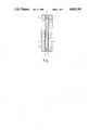
- FIGUREis a cross-sectional view of a display wall of the invention and a formula sheet.
- FIGURE of whichis cross-sectional view of a picture display cell according to the invention and the formula sheet.
- Reference numerals 1 and 2 in the FIGUREdenote two oppositely relocated plates which are transparent to light and which are hereinafter referred to as substrates and which on the facing sides comprise electrodes 4 and 5, for example, manufactured of In 2 O 3 SnO 2 .
- An orientation layer 7 with which preferably nematic liquid crystals 6 can be orientedis provided on the facing sides of these electrodes.
- the cellis formed by placing the substrates thus formed with electrodes and orientation layer opposite to each other and sealing the aperture by means of a ring and filling the space between the substrates and the ring 3 with the liquid crystalline material 6.
- a layer of adhesive of an epoxy compoundis often used as the ring 3.
- the inventionresides in the fact that a liquid crystalline monomer is provided on a substrate and is oriented in an electric or magnetic field after the liquid crystalline monomer has been provided in a liquid crystalline phase and after the orientation the monomer is polymerized, possibly by exposure to actinic light.
- Another methodis to heat the monomer up to a temperature above the nematic-isotropic transition state and then cool it in the field down to a temperature at which the monomer is again liquid crystalline, after which the polymerization is carried out.
- Dependent on the angle of the optical axis of the nematic groups the polymer layerinduces tilted orientation in the subsequently provided liquid crystal material.
- the orientation layermay be started from a liquid film of a crystalline (meth)acrylate monomer.
- This monomercan be dissolved and the resulting solution can then be provided on the substrate in the form of a thin film according to a known spinning technique.
- An useful example of such an acrylate monomeris represented by the formula 4 of the formula sheet.
- liquid crystalline meth(acrylate)monomercorresponds to the formulae 2 and 3 of the formula sheet.
- the monomers of the formulae 2 and 3are diacrylates which upon polymerization form a cross-linked structure.
- the monomers of formulae 2 and 3are novel products.
- the inventionalso relates to these novel products.
- the monomers of formula 2can be prepared by a chemical process represented by reaction scheme 12 of the formula sheet.
- the monomers of formula 3can be manufactured according to the reaction scheme 13 of the formula sheet.
- the several reactionsare, as usual, performed in the presence of inert organic solvents such as ketones, ethers or hydrocarbons.
- the reaction A and B of scheme 12are performed in the presence of an amine, particularly a mixture (10:1) of triethyamine and 1-dimethylamino-pyridine.
- the reaction A of scheme 13is performed in the presence of NaOH and NaI.
- the reactions C and E of scheme 13are performed in the presence of an amine as denoted above for scheme 12.
- R 1has the meaning disclosed hereinbefore and Alk stands for an alkylene group.
- the monomerFor the orientation of the mesogenic groups of the monomer in the electric or the magnetic field, the monomer must be to the liquid crystalline phase, which is possible by raising the temperature.
- the transition from the crystalline to the nematic statetakes place at 89° C. and from the nematic to the isotropic state at 98,5° C. upon heating the monomer, while upon cooling the transition from the isotropic state to the nematic state takes place at 98° C., the transition from the nematic to the smectic state at 78° C. and from the smectic state to the crystalline state at 49° C.
- the orientation and the in situ polymerizationpreferably take place at a temperature of 89°-98° C. dependent on the desired state of the orientation layer.
- the transition in a heating cycle from the crystalline to the smectic statetakes place at 17° C. and from smectic to the nematic state at 93° C. and from nematic to the isotropic state at 193° C. Therefore, the orientation for the monomer of formula 4 will take place at a temperature between 77° and 153° C.
- the compound of the formula 6shows a transition from the crystalline to the nematic at 129° C. and from the nematic state to the isotropic at 149° C.
- the temperature at which the orientation of the monomer, notably the mesogenic group, has to be carried outmay be reduced by using a mixture of monomers in which not only the orientation takes place separately but can also take place at a comparatively low temperature, possibly at the ambient temperature.
- a further modificationis the use of a mixture of a polymer in a monomer in which the polymer may be constructed from other monomers than the monomer which is used here as a solvent.
- the polymerization of the oriented monomerpreferably takes place by exposure to actinic light, notably by exposure to UV-light.
- the polymerizationcan be accelerated by adding to the acrylate monomers a small quantity, preferably less than 10% by weight, of a photoinitiator.
- the polymerizationpreferably takes place while excluding oxygen.
- the orientation of the mesogenic groupsis fixed so that said anisotropy is maintained within a wide temperature range.
- the photoinitiators to be usedare known an example of which is is is Irgacure 651 (trademark of CIBA-Geigy).
- a bonding layerwhich may consist of a -methacryloxypropyl trimethoxysilane or -aminopropylsilane.
- Another embodiment which is to be preferredis to carry out the polymerization in the presence of a photoinitiator which, however, is not mixed with the monomer but which photoinitiator is bound to the surface so that no changes of the liquid crystalline properties of the monomer are obtained in that it is mixed with the non-liquid crystalline photoinitiator and moreover the polymerization then takes place from the surface and the polymer chains are bound to the surface. In this manner it is prevented that the polymer is optionally dissolved in the liquid crystalline material 6 of the display cell.
- the photo initiatormay be bound to the surface by first providing the substrate, according to a known method, with a layer of an -aminopropylsilane, after which the substrate is immersed in a solution of a photo initiator in THF (tetrahydrofuran), for which purpose a 5% solution of the photoinitiator of formula 9 may be used.
- THFtetrahydrofuran
- a 5% solution of the photoinitiator of formula 9may be used.
- the substrateis provided with a surface film of a material which comprises both an amino group and a benzophenone group, which amino group has an accelerating effect on the photoinitiator of the benzophenone group.
- the actinic radiationis carried out with electron radiation it is not necessary to use an initiator.
- the orientation of the mesogenic group in the monomerhas to be carried out at a comparatively high temperature, the disadvantage of this is that at the said comparatively high temperature the possibility of polymerization rather occurs so that it is to be preferred to perform the orientation at a comparatively low temperature and then to freeze the oriented monomeric groups by polymerization.
Landscapes
- Physics & Mathematics (AREA)
- Chemical & Material Sciences (AREA)
- Nonlinear Science (AREA)
- Spectroscopy & Molecular Physics (AREA)
- General Physics & Mathematics (AREA)
- Crystallography & Structural Chemistry (AREA)
- Mathematical Physics (AREA)
- Optics & Photonics (AREA)
- Engineering & Computer Science (AREA)
- Materials Engineering (AREA)
- Organic Chemistry (AREA)
- Liquid Crystal (AREA)
- Addition Polymer Or Copolymer, Post-Treatments, Or Chemical Modifications (AREA)
- Macromonomer-Based Addition Polymer (AREA)
Abstract
Description
This is a continuation of application Ser. No. 092,253, filed Sept. 1, 1987 now abandoned.
The invention relates to a picture display cell comprising as a substrate two orthogonally relocated plates which are transparent to light and which on the facing sides comprise an electrode of a material which is transparent to light and having an orientation layer, a sealing ring positioned between the ends of the plates, a liquid crystalline material being provided in the space between the plates and the ring. The invention further relates to a method of forming an orientation layer on a substrate for the picture display cell comprising an electrode and to the materials from which the orientation layer is manufactured.
Such a picture display cell is known from U.S. Pat. No. 4,469,409 in which picture display cell an orientation layer is provided on a glass substrate, which orientation layer is formed from a film of a homogeneous mixture having a silanol oligomer modified with an aromatic ring which comprises a silane group and an organic polymer. The picture display cell of the twisted nematic type (TN-type) according to the said U.S. Patent comprises a substrate having an orientation layer which can withstand elevated temperatures better and bonds more satisfactorily to the substrate in the previously used organic polymers having an imide or quinazoline ring and bonds more satisfactorily in the substrate. A method of providing a polymeric layer on a substrate is described in example 1 of this U.S. Patent in which a solution of the polymer is prepared and this solution is provided on the substrate via a spinning technique.
German Auslegeschrift 2,315,541 discloses a picture display cell in which on the substrate an orientation layer is provided by vapour deposition at reduced pressure. According to this vapour deposition technique SiOx layers are provided. More information on such layers is shown in H. A. van Sprang and R. G. Aartsen in J. Appl. Phys. 56 (2), July 15, 1984, pp. 251-262, in which article the method of providing, the measurements and the apparatus used are described.
The use of such an SiOx orientation layer in a picture display cell, however, has for a disadvantage or in that with these cells only a restricted range of solid angles for the orientation of the nematic liquid crystal material is available.
German Offenlegungschrift 3,020,645 discloses a picture display cell in which a polymeric orientation layer is provided on the substrate, which polymeric orientation layer itself is liquid crystalline. When switching on or off the voltage the liquid crystalline material and the polymeric layer are both oriented at right angles to or parallel to the substrate. The orientation layer is also in the liquid crystalline phase under operating conditions.
Japanese Patent Application Kokai No. 52-146255 discloses a picture display cell having a liquid crystalline material in which the orientation of the liquid crystalline material takes place by incorporating herein magnetic particles, for example, --Fe2 O3 acicular particles which are oriented by means of a magnet, after which the temperature of the glass plates is raised so that the liquid binder at the raised temperature is made to solidify. In this manner the magnetic particles are fixed and hence also the liquid crystal material. The presence of the acicular --Fe2 O3 -particles in the picture display cell, however, has disadvantages because under the influence of said particles inteferences in the light permeability can easily occur.
Applicants have made further research into the orientation layer of the picture display cell and they have found that it is possible to provide a polymeric layer on the substrate, which polymeric layer can be oriented and fixed after the orientation. As specific examples of polymers that may be used are the specific materials described inter alia by R. Simon and H. J. Coles in Mol. Cryst. Liq. Cryst. Vol. 102 (Letters), pp. 43-48. This method yielded good results but had the disadvantage that it took some time, for example, 5 minutes to more than 1 hour, dependent on the polymer used, until the orientation layer had been oriented completely in an electric or magnetic field.
According to the invention Applicants have found that it is possible to considerably reduce said time necessary for the orientation, namely to even a few seconds, by forming a picture display cell according to the invention as described in the opening paragraph which is characterized in that the orientation layer is formed from a monomer or low molecular compound which is first oriented in a magnetic or electric field and is then polymerized. According to the invention, the method of forming an orientation layer on a substrate which comprises an electrode for a picture display cell is therefore characterized in that a film of a liquid crystalline monomer is provided, the monomer is oriented at a given angle in a magnetic or an electric field and is then polymerized.
Present in the drawing is a FIGURE which is a cross-sectional view of a display wall of the invention and a formula sheet.
The invention will now be described in greater detail with reference to the ensuing description and the drawing, the FIGURE of which is cross-sectional view of a picture display cell according to the invention and the formula sheet.
Essentially the invention resides in the fact that a liquid crystalline monomer is provided on a substrate and is oriented in an electric or magnetic field after the liquid crystalline monomer has been provided in a liquid crystalline phase and after the orientation the monomer is polymerized, possibly by exposure to actinic light. Another method is to heat the monomer up to a temperature above the nematic-isotropic transition state and then cool it in the field down to a temperature at which the monomer is again liquid crystalline, after which the polymerization is carried out. Dependent on the angle of the optical axis of the nematic groups the polymer layer induces tilted orientation in the subsequently provided liquid crystal material.
More in particular it has been found that, the orientation layer, may be started from a liquid film of a crystalline (meth)acrylate monomer. This monomer can be dissolved and the resulting solution can then be provided on the substrate in the form of a thin film according to a known spinning technique. A suitable group of liquid crystalline acrylate monomers is represented byformula 1 of the formula sheet, in which formula --A-- is a bivalent radical, for example, (CH2)x, (CH2)x O, (Si(CH3)2 --O)x, wherein x=1-15 and (CH2 --CH2 --O)y, wherein y=1 to 8 and --B-- is a mesogenic group, for example, a group offormulae formula 4 of the formula sheet.
In a preferred embodiment of the picture display cell according to the invention the liquid crystalline meth(acrylate)monomer corresponds to theformulae formulae
The monomers offormulae formula 2 can be prepared by a chemical process represented by reaction scheme 12 of the formula sheet. The monomers offormula 3 can be manufactured according to thereaction scheme 13 of the formula sheet. The several reactions are, as usual, performed in the presence of inert organic solvents such as ketones, ethers or hydrocarbons. The reaction A and B of scheme 12 are performed in the presence of an amine, particularly a mixture (10:1) of triethyamine and 1-dimethylamino-pyridine. The reaction A ofscheme 13 is performed in the presence of NaOH and NaI. The reactions C and E ofscheme 13 are performed in the presence of an amine as denoted above for scheme 12. Inschemes 12 and 13, R1 has the meaning disclosed hereinbefore and Alk stands for an alkylene group.
Useful examples of the diacrylate monomers are given by theformulae
For the orientation of the mesogenic groups of the monomer in the electric or the magnetic field, the monomer must be to the liquid crystalline phase, which is possible by raising the temperature. For the acrylate offormula 4, shown on the formula sheet, the transition from the crystalline to the nematic state takes place at 89° C. and from the nematic to the isotropic state at 98,5° C. upon heating the monomer, while upon cooling the transition from the isotropic state to the nematic state takes place at 98° C., the transition from the nematic to the smectic state at 78° C. and from the smectic state to the crystalline state at 49° C. This means that the orientation and the in situ polymerization preferably take place at a temperature of 89°-98° C. dependent on the desired state of the orientation layer.
For the acrylate monomer shown in the formula sheet byformula 5, the transition in a heating cycle from the crystalline to the smectic state takes place at 17° C. and from smectic to the nematic state at 93° C. and from nematic to the isotropic state at 193° C. Therefore, the orientation for the monomer offormula 4 will take place at a temperature between 77° and 153° C.
The compound of theformula 6 shows a transition from the crystalline to the nematic at 129° C. and from the nematic state to the isotropic at 149° C.
The temperature at which the orientation of the monomer, notably the mesogenic group, has to be carried out may be reduced by using a mixture of monomers in which not only the orientation takes place separately but can also take place at a comparatively low temperature, possibly at the ambient temperature. A further modification is the use of a mixture of a polymer in a monomer in which the polymer may be constructed from other monomers than the monomer which is used here as a solvent.
The polymerization of the oriented monomer preferably takes place by exposure to actinic light, notably by exposure to UV-light. The polymerization can be accelerated by adding to the acrylate monomers a small quantity, preferably less than 10% by weight, of a photoinitiator. The polymerization preferably takes place while excluding oxygen. As a result of the polymerization the orientation of the mesogenic groups is fixed so that said anisotropy is maintained within a wide temperature range.
The photoinitiators to be used are known an example of which is is Irgacure 651 (trademark of CIBA-Geigy).
It may be advantageous not to provide the film of the monomer directly on the substrate material but first to provide the substrate material with a bonding layer which may consist of a -methacryloxypropyl trimethoxysilane or -aminopropylsilane. Another embodiment which is to be preferred is to carry out the polymerization in the presence of a photoinitiator which, however, is not mixed with the monomer but which photoinitiator is bound to the surface so that no changes of the liquid crystalline properties of the monomer are obtained in that it is mixed with the non-liquid crystalline photoinitiator and moreover the polymerization then takes place from the surface and the polymer chains are bound to the surface. In this manner it is prevented that the polymer is optionally dissolved in the liquidcrystalline material 6 of the display cell.
The photo initiator may be bound to the surface by first providing the substrate, according to a known method, with a layer of an -aminopropylsilane, after which the substrate is immersed in a solution of a photo initiator in THF (tetrahydrofuran), for which purpose a 5% solution of the photoinitiator offormula 9 may be used. At the ambient temperature reaction takes place between the -aminopropylsilane and the compound offormula 9, so that the substrate is provided with a surface film of a material which comprises both an amino group and a benzophenone group, which amino group has an accelerating effect on the photoinitiator of the benzophenone group.
If the actinic radiation is carried out with electron radiation it is not necessary to use an initiator. When the orientation of the mesogenic group in the monomer has to be carried out at a comparatively high temperature, the disadvantage of this is that at the said comparatively high temperature the possibility of polymerization rather occurs so that it is to be preferred to perform the orientation at a comparatively low temperature and then to freeze the oriented monomeric groups by polymerization.
Claims (12)
1. A picture display cell comprising as a substrate two oppositely located plates which are transparent to light and which on the facing sides comprise an electrode of a material which is transparent to light having thereon an orientation layer and a sealing ring between the ends of the plate, a liquid crystalline material being provided in the space between the plates and the ring, characterized in that the orientation layer is formed from a monomer or a low molecular weight compound which is first oriented at a given angle essentially only in an electric or magnetic field and is then polymerized.
2. A picture display cell as claimed in claim 1, characterized in that the orientation layer is built up from a polymer obtained by the polymerization of oriented liquid crystalline (meth)acrylate monomers.
3. A picture display cell as claimed in claims 1 or 2, characterized in that the monomers are acrylate monomers which correspond to formula 1, 2 or 3 of the formula sheet, wherein--A--is a bivalent radical, --B--is a mesogenic group, R is hydrogen atom or a methyl group and R2 is an alkyl group, an aromatic group, a cyano group or combinations thereof.
4. A picture display cell as claimed in claim 3, characterized in that the acrylate monomers correspond to formula 4, 5 or 6 of the formula sheet.
5. A picture display cell as claimed in claims 1 or 2, characterized in that the orientation layer is formed from a mixture of two or more monomers which are polymerized.
6. A method of forming an orientation layer on a substrate for a picture display cell comprising an electrode, characterized in that a film of a liquid crystalline monomer is provided in the substrate, the monomer is oriented essentially in a magnetic or electric field at a given angle, and is then polymerized.
7. A method as claimed in claim 6, characterized in that the polymerization is carried out by exposure to actinic light.
8. A method as claimed in claims 6 or 7, characterized in that a photo initiator is added to a monomer in a quantity smaller than 10% by weight calculated on the monomer.
9. A method as claimed in claim 6 or 7, characterized in that monomers are used as stated in claim 6.
10. A method as claimed in claim 6 or 7, characterized in that a bonding layer is formed on the substrate before the monomeric film is provided.
11. A method as claimed in claim 8, characterized in that the photoinitiator is bonded to the surface of the substrate and is not mixed in the monomer.
12. A method as claimed in claim 11, characterized in that the substrate is provided with a bonding agent, then with a photoinitiator, after which a monomeric film is provided and after orientation the polymerization of the monomeric film is carried out under the influence of UV-rays.
Applications Claiming Priority (2)
| Application Number | Priority Date | Filing Date | Title |
|---|---|---|---|
| NL8602235 | 1986-09-04 | ||
| NL8602235 | 1986-09-04 |
Related Parent Applications (1)
| Application Number | Title | Priority Date | Filing Date |
|---|---|---|---|
| US07092253Continuation | 1987-09-01 |
Publications (1)
| Publication Number | Publication Date |
|---|---|
| US4892392Atrue US4892392A (en) | 1990-01-09 |
Family
ID=19848498
Family Applications (1)
| Application Number | Title | Priority Date | Filing Date |
|---|---|---|---|
| US07/267,694Expired - LifetimeUS4892392A (en) | 1986-09-04 | 1988-11-02 | Picture display cell and method of forming an orientation layer on a substrate of the picture display cell |
Country Status (3)
| Country | Link |
|---|---|
| US (1) | US4892392A (en) |
| EP (1) | EP0261712A1 (en) |
| JP (1) | JPH083586B2 (en) |
Cited By (30)
| Publication number | Priority date | Publication date | Assignee | Title |
|---|---|---|---|---|
| US4983479A (en)* | 1988-02-29 | 1991-01-08 | U.S. Philips Corporation | Method of manufacturing a laminated element and the element thus obtained |
| US5178710A (en)* | 1988-11-02 | 1993-01-12 | U.S. Philips Corporation | Bonding using a difunctional liquid crystalline monomer adhesive under an applied force field |
| US5247379A (en)* | 1989-02-16 | 1993-09-21 | S. T. Lagerwall S.A.R.L. | Chiral nematic liquid crystal device with linear electroclinic effect |
| US5262882A (en)* | 1991-03-26 | 1993-11-16 | U.S. Philips Corporation | Liquid crystal device orientation layer of an oriented polymer network containing liquid crystal |
| US5438421A (en)* | 1991-04-24 | 1995-08-01 | Alps Electric Co., Ltd. | Orientation film of liquid crystal having bilaterally asymmetric ridges separated by grooves |
| US5468519A (en)* | 1992-12-11 | 1995-11-21 | Sharp Kabushiki Kaisha | Method for forming an orientation film including coupling an organic compound to a silane coupling agent in a magnetic or electrical field |
| US5486403A (en)* | 1993-04-02 | 1996-01-23 | Alps Electric Co., Ltd. | Alignment layer for liquid crystal element and method of producing same |
| WO1996009567A1 (en)* | 1994-09-20 | 1996-03-28 | Philips Electronics N.V. | Manufacture of a substrate having a modified orientation layer and of a liquid crystalline display device comprising such a substrate |
| US5541039A (en)* | 1989-12-26 | 1996-07-30 | Alliedsignal Inc. | Method for forming optically active waveguides |
| US5707691A (en)* | 1996-08-27 | 1998-01-13 | The Coca-Cola Company | Coating hollow containers by in-situ polymerization of monomers in bi-axially orientated form |
| US5725915A (en)* | 1994-09-21 | 1998-03-10 | Alps Electric Co., Ltd. | Liquid crystal display |
| US5742370A (en)* | 1996-09-12 | 1998-04-21 | Korea Institute Of Science And Technology | Fabrication method for liquid crystal alignment layer by magnetic field treatment |
| US5846452A (en)* | 1995-04-06 | 1998-12-08 | Alliant Techsystems Inc. | Liquid crystal optical storage medium with gray scale |
| US5851471A (en)* | 1996-05-16 | 1998-12-22 | The Coca-Cola Company | Method for injection molding a multi-layer preform for use in blow molding a plastic bottle |
| US5863457A (en)* | 1993-12-24 | 1999-01-26 | Dainippon Ink And Chemicals, Inc. | Polymerizable liquid crystal composition and optically anisotropic film comprising the same |
| US5965081A (en)* | 1996-05-16 | 1999-10-12 | The Coca-Cola Company | Method of making side-gated preforms for use in blow molding plastic bottles |
| US20010022998A1 (en)* | 1996-09-17 | 2001-09-20 | Merck Patent Gesellschaft Mit Beschrankter Haftung | Anisotropic polymer layer |
| US6404476B1 (en)* | 1989-09-01 | 2002-06-11 | Semiconductor Energy Laboratory Co., Ltd. | Device having an improved connective structure between two electrodes |
| US6495221B1 (en)* | 1997-07-31 | 2002-12-17 | Matsushita Electric Industrial Co., Ltd. | Chemisorptive substance, aligned liquid-crystal film and liquid-crystal display element both made by using the same, and processes for producing these |
| US20040075082A1 (en)* | 1999-08-31 | 2004-04-22 | Canon Kabushiki Kaisha | Single-crystalline film and process for production thereof |
| US6833166B2 (en)* | 2001-07-10 | 2004-12-21 | Koninklijke Philips Electronics N.V. | Anisotropic composite comprising a mixture of a polymeric network and an inorganic material |
| WO2005008324A1 (en)* | 2003-07-18 | 2005-01-27 | Koninklijke Philips Electronics N.V. | Liquid crystal display device comprising an anchoring layer |
| US20060016516A1 (en)* | 2004-07-21 | 2006-01-26 | Beck Patricia A | Method for preparation of anisotropic materials |
| US20060176431A1 (en)* | 2005-02-07 | 2006-08-10 | Kim Chang D | Method and apparatus for forming alignment layer for liquid crystal display |
| US20060176432A1 (en)* | 2005-02-07 | 2006-08-10 | Kim Chang D | Method and apparatus of forming alignment layer for liquid crystal display device |
| US20060198969A1 (en)* | 2005-03-07 | 2006-09-07 | Lg.Philips Lcd Co., Ltd. | Method of forming alignment layer for liquid crystal display and liquid crystal display fabricated using the same |
| US20070064176A1 (en)* | 2005-09-15 | 2007-03-22 | Semiconductor Energy Laboratory Co., Ltd. | Manufacturing method of liquid crystal display device |
| US20110116020A1 (en)* | 2008-07-14 | 2011-05-19 | Universite Laval | Surface programming method and light modulator devices made thereof |
| US20110122362A1 (en)* | 2008-07-14 | 2011-05-26 | Lensvector Inc. | Liquid crystal lens using surface programming |
| CN108681158A (en)* | 2018-05-21 | 2018-10-19 | 南京中电熊猫平板显示科技有限公司 | One kind is from orientation display device and its alignment method |
Families Citing this family (88)
| Publication number | Priority date | Publication date | Assignee | Title |
|---|---|---|---|---|
| NL8901167A (en)* | 1989-05-10 | 1990-12-03 | Philips Nv | METHOD FOR MANUFACTURING A POLARIZATION FILTER, A POLARIZATION FILTER SO OBTAINED AND A DISPLAY EQUIPPED WITH THE POLARIZATION FILTER. |
| US5078910A (en)* | 1989-06-20 | 1992-01-07 | Edison Polymer Innovation Corp. | Polimerization of liquid crystalline monomers |
| US5073294A (en) | 1990-03-07 | 1991-12-17 | Hercules Incorporated | Process of preparing compositions having multiple oriented mesogens |
| NL9000808A (en)* | 1990-04-06 | 1991-11-01 | Koninkl Philips Electronics Nv | LIQUID CRYSTALLINE MATERIAL AND IMAGE DISPLAY CELL CONTAINING THIS MATERIAL. |
| EP0476543B1 (en)* | 1990-09-17 | 1996-08-28 | Matsushita Electric Industrial Co., Ltd. | Liquid crystal alignment film and method of manufacturing the same |
| US5256456A (en)* | 1990-09-17 | 1993-10-26 | Matsushita Electric Industrial Co., Ltd. | Liquid crystal alignment film and method of manufacturing the same |
| TW240240B (en)* | 1992-03-27 | 1995-02-11 | Philips Nv | |
| DE4405316A1 (en)* | 1994-02-19 | 1995-08-24 | Basf Ag | New polymerizable liquid crystalline compounds |
| DE4408170A1 (en)* | 1994-03-11 | 1995-09-14 | Basf Ag | New polymerizable liquid crystalline compounds |
| JP3954098B2 (en)* | 1995-02-06 | 2007-08-08 | メルク パテント ゲゼルシャフト ミット ベシュレンクテル ハフトング | Bireactive mesogenic compounds and intermediates |
| GB9514970D0 (en)* | 1995-07-21 | 1995-09-20 | Secr Defence | Liquid crystal polymer devices and materials |
| GB2317965B (en)* | 1995-07-21 | 2000-02-16 | Secr Defence | Liquid crystal polymer devices and materials |
| KR0182876B1 (en) | 1996-01-09 | 1999-05-01 | 구자홍 | Method for controlling pretilt direction for lcd cell |
| DE19611101A1 (en)* | 1996-03-21 | 1997-09-25 | Basf Ag | Chiral connections |
| US6217792B1 (en)* | 1996-07-01 | 2001-04-17 | Merck Patent Gmbh | Chiral dopants |
| US6191836B1 (en) | 1996-11-07 | 2001-02-20 | Lg Philips Lcd, Co., Ltd. | Method for fabricating a liquid crystal cell |
| US6292296B1 (en) | 1997-05-28 | 2001-09-18 | Lg. Philips Lcd Co., Ltd. | Large scale polarizer and polarizer system employing it |
| GB2330214A (en)* | 1997-10-08 | 1999-04-14 | Secr Defence | Bistable nematic liquid crystal device |
| GB2330213A (en)* | 1997-10-08 | 1999-04-14 | Secr Defence | Twisted Nematic Liquid crystal device |
| KR100259258B1 (en) | 1997-11-21 | 2000-06-15 | 구본준 | Liquid crystal display device |
| US7061679B1 (en) | 1998-05-27 | 2006-06-13 | Lg. Philips Lcd Co., Ltd. | Light irradiating device |
| SE517919C2 (en)* | 1998-07-08 | 2002-08-06 | Ecsibeo Ab | Liquid crystal device and method for its preparation and use |
| US6723393B1 (en) | 1998-10-20 | 2004-04-20 | Asahi Glass Company, Limited | Liquid crystal optical element and method for preparing the same |
| KR100301853B1 (en) | 1999-03-25 | 2001-09-26 | 구본준, 론 위라하디락사 | Alignment layer for liquid crystal display device |
| KR100357214B1 (en) | 1999-04-21 | 2002-10-18 | 엘지.필립스 엘시디 주식회사 | Liquid crystal display device |
| KR100475107B1 (en) | 1999-10-14 | 2005-03-09 | 엘지.필립스 엘시디 주식회사 | A method of manufacturing a multi-domain liquid crystal display device |
| JP2002069450A (en)* | 2000-08-29 | 2002-03-08 | Dainippon Ink & Chem Inc | Polymerizable liquid crystal composition |
| KR100595300B1 (en) | 2000-10-28 | 2006-07-03 | 엘지.필립스 엘시디 주식회사 | Optical alignment material and liquid crystal display device using same |
| KR100565739B1 (en) | 2000-10-28 | 2006-03-29 | 엘지.필립스 엘시디 주식회사 | Optical alignment material and liquid crystal display device using same |
| JP2003161835A (en) | 2001-07-02 | 2003-06-06 | Merck Patent Gmbh | Optical variable marking |
| US6824706B2 (en) | 2001-07-25 | 2004-11-30 | Merck Patent Gesellschaft Mit Beschrank Haftung | Mono-, Oligo- and poly-difluorovinyl-(hetero)arylenes, their synthesis and their use as charge transport materials |
| KR20030010508A (en) | 2001-07-25 | 2003-02-05 | 메르크 파텐트 게엠베하 | Mono-, oligo- and poly-4-fluorothiophenes and their use as charge transport materials |
| ATE409714T1 (en) | 2001-07-25 | 2008-10-15 | Merck Patent Gmbh | MONO-, OLIGO AND POLY-3-(1,1-DIFLUOROALKYL)THIOPHENES AND THEIR USE AS CHARGE TRANSPORT MATERIAL |
| TWI245795B (en) | 2001-08-17 | 2005-12-21 | Merck Patent Gmbh | Mono-, oligo- and polyalkylidenefluorenes and their use as charge transport materials |
| ATE473251T1 (en) | 2001-09-29 | 2010-07-15 | Merck Patent Gmbh | MONO-, OLIGO- AND POLYMERS OF BENZO(B)THIOPHENE AND 2,2'-BISBENZOTHIOPHENE AND THEIR USE AS CHARGE TRANSPORT MATERIAL |
| JP2004002288A (en) | 2001-12-13 | 2004-01-08 | Merck Patent Gmbh | Oxadiazole derivative and use thereof as charge transfer material and luminescent material |
| DE10257711B4 (en) | 2001-12-27 | 2019-09-26 | Merck Patent Gmbh | Polymerizable monocyclic compounds containing liquid crystal mixtures |
| DE60336184D1 (en) | 2002-02-06 | 2011-04-14 | Merck Patent Gmbh | Birefringent film and its use |
| EP2209027A1 (en) | 2002-02-13 | 2010-07-21 | MERCK PATENT GmbH | Security marking comprising an anisotropic polymer film on a substrate with a structured surface |
| DE60332784D1 (en) | 2002-02-13 | 2010-07-15 | Merck Patent Gmbh | A method of making an anisotropic polymer film on a substrate having a structured surface |
| ATE328049T1 (en)* | 2002-03-04 | 2006-06-15 | Fuji Photo Film Co Ltd | POLYMERIZABLE LIQUID CRYSTAL COMPOUND, LIQUID CRYSTAL POLYMER AND APPLICATIONS THEREOF |
| TWI258603B (en) | 2002-04-23 | 2006-07-21 | Nitto Denko Corp | Polarized light device, polarized light source and image display apparatus using the same |
| DE60305570T2 (en) | 2002-04-24 | 2007-05-03 | Merck Patent Gmbh | Reactive mesogenic benzodithiophenes |
| KR100839402B1 (en) | 2002-07-23 | 2008-06-20 | 닛토덴코 가부시키가이샤 | Optical film and liquid crystal display device using same |
| US7046443B2 (en) | 2002-07-24 | 2006-05-16 | Nitto Denko Corporation | Anisotropic light scattering element, anisotropic light scattering polarizing plate using the same, and image display device using the same |
| DE10251861A1 (en) | 2002-11-07 | 2004-05-19 | Consortium für elektrochemische Industrie GmbH | Polymerizable mixture containing a monomer or oligomer useful for optical applications, e.g. wavelength and polarization selective, and phase lag, optical elements for electromagnetic radiation, and for liquid crystal displays |
| EP1431050A3 (en) | 2002-12-19 | 2004-11-03 | MERCK PATENT GmbH | Process for laser marking of a liquid crystal film |
| CN101316876A (en) | 2005-11-24 | 2008-12-03 | 默克专利股份有限公司 | regioregular polyselenophene |
| US7879256B2 (en) | 2006-03-31 | 2011-02-01 | E. I. Du Pont De Nemours And Company | Liquid crystal compositions, polymer networks derived therefrom and process for making the same |
| US7914700B2 (en) | 2006-03-31 | 2011-03-29 | E. I. Du Pont De Nemours And Company | Liquid crystal compositions and polymer networks derived therefrom |
| TW200811492A (en) | 2006-07-12 | 2008-03-01 | Nitto Denko Corp | Polarizing plate with optical compensation layer, method of producing the same, and liquid crystal panel, liquid crystal display, and image display including the same |
| JP2010536782A (en) | 2007-08-15 | 2010-12-02 | イー・アイ・デュポン・ドウ・ヌムール・アンド・カンパニー | Chiral compounds, liquid crystal compositions and polymer networks derived therefrom |
| WO2009023762A1 (en) | 2007-08-15 | 2009-02-19 | E. I. Du Pont De Nemours And Company | Alkaloid monomers, liquid crystal compositions and polymer networks derived therefrom |
| DE102008039745A1 (en) | 2007-09-07 | 2009-03-12 | Merck Patent Gmbh | Process for the preparation of a homogeneous liquid mixture |
| EP2065361B1 (en) | 2007-11-30 | 2014-12-17 | Merck Patent GmbH | Polymerisable compounds |
| KR101631045B1 (en) | 2008-02-29 | 2016-06-15 | 메르크 파텐트 게엠베하 | Alignment film for liquid crystals obtainable by direct particle beam deposition |
| ATE528377T1 (en) | 2008-03-05 | 2011-10-15 | Merck Patent Gmbh | LIQUID CRYSTALLINE MEDIUM AND LIQUID CRYSTAL DISPLAY WITH TWISTED YARN |
| US7988881B2 (en) | 2008-09-30 | 2011-08-02 | E. I. Du Pont De Nemours And Company | Multilayer laminates comprising chiral nematic liquid crystals |
| EP2218764B1 (en) | 2009-02-13 | 2012-01-18 | Merck Patent GmbH | Chiral reactive mesogen mixture |
| US20120013831A1 (en) | 2009-03-26 | 2012-01-19 | Merck Patent Gmbh | Process of preparing an anisotropic multilayer using particle beam alignment |
| EP2320268A1 (en) | 2009-10-26 | 2011-05-11 | Merck Patent GmbH | Alignment layer for planar alignment of a polymerizable liquid crystalline or mesogenic material |
| KR101779226B1 (en) | 2009-10-30 | 2017-09-18 | 메르크 파텐트 게엠베하 | Polymerisable lc material and polymer film with negative optical dispersion |
| WO2011078055A1 (en) | 2009-12-24 | 2011-06-30 | 日東電工株式会社 | Process for production of broad-band cholesteric liquid crystal film |
| US20130029169A1 (en) | 2010-03-30 | 2013-01-31 | Merck Patent Gesellschaft Mit Beschrankter Haftung | Method for producing multicoloured coatings |
| EP2399972B1 (en) | 2010-06-25 | 2015-11-25 | Merck Patent GmbH | Liquid-crystalline medium and liquid-crystal display having high twist |
| WO2012152409A1 (en) | 2011-05-09 | 2012-11-15 | Merck Patent Gmbh | Reactive mesogen based polymer particles |
| DE102012011464A1 (en) | 2012-06-12 | 2013-12-12 | Merck Patent Gmbh | Method for producing three-dimensional patterns in liquid-crystalline coatings |
| US10100253B2 (en) | 2012-06-26 | 2018-10-16 | Merck Patent Gmbh | Method of preparing a birefringent polymer film |
| EP3060947B1 (en) | 2013-10-21 | 2021-04-14 | Merck Patent GmbH | Method of preparing a birefringent polymer film |
| DE102013018094A1 (en) | 2013-12-03 | 2015-06-03 | Merck Patent Gmbh | Mixing device and its use |
| DE102013020400A1 (en) | 2013-12-10 | 2015-06-11 | Merck Patent Gmbh | cleaning device |
| DE102013020638A1 (en) | 2013-12-16 | 2015-06-18 | Merck Patent Gmbh | Filling device and its use for filling a fluid |
| DE102013021279A1 (en) | 2013-12-18 | 2015-06-18 | Merck Patent Gmbh | Process for cleaning a liquid crystal mixture |
| US20170343847A1 (en) | 2014-11-06 | 2017-11-30 | Merck Patent Gmbh | Light modulation element |
| CN107003578B (en) | 2014-12-19 | 2021-03-23 | 默克专利股份有限公司 | Light modulation element |
| WO2016116123A1 (en) | 2015-01-23 | 2016-07-28 | Merck Patent Gmbh | Light modulation element |
| EP3248061B1 (en) | 2015-01-23 | 2020-10-14 | Merck Patent GmbH | Light modulation element |
| US20180188586A1 (en) | 2015-07-02 | 2018-07-05 | Merck Patent Gmbh | Process of preparing a light modulation element |
| WO2017001041A1 (en) | 2015-07-02 | 2017-01-05 | Merck Patent Gmbh | Process of preparing a light modulation element |
| WO2017059942A1 (en) | 2015-10-06 | 2017-04-13 | Merck Patent Gmbh | Chiral compounds |
| WO2017198586A1 (en) | 2016-05-17 | 2017-11-23 | Merck Patent Gmbh | Light modulation element |
| TWI747947B (en) | 2016-09-05 | 2021-12-01 | 德商馬克專利公司 | Uv curable adhesion promoters based on functionalised polyvinyl alcohols |
| WO2018099883A1 (en) | 2016-12-01 | 2018-06-07 | Merck Patent Gmbh | Polymerisable lc medium and polymer film with flat optical dispersion |
| WO2018073459A2 (en) | 2017-03-28 | 2018-04-26 | Merck Patent Gmbh | Liquid crystal device |
| EP3612615B1 (en) | 2017-04-20 | 2024-10-16 | Merck Patent GmbH | Light modulation element |
| WO2019121368A1 (en) | 2017-12-18 | 2019-06-27 | Merck Patent Gmbh | Liquid crystal medium and liquid crystal device |
| JP2023035529A (en) | 2021-09-01 | 2023-03-13 | 日東電工株式会社 | Polymer dispersion type liquid crystal film and method for manufacturing polymer dispersion type liquid crystal film |
| JP2025070267A (en) | 2023-10-19 | 2025-05-02 | 日東電工株式会社 | Elliptical polarizing plate and image display device |
Citations (18)
| Publication number | Priority date | Publication date | Assignee | Title |
|---|---|---|---|---|
| US3989354A (en)* | 1973-10-19 | 1976-11-02 | Thomson-Csf | Nematic liquid crystal of homeotropically aligned type and a method of manufacturing said device |
| US4022934A (en)* | 1975-04-21 | 1977-05-10 | Hughes Aircraft Company | Means for inducing perpendicular alignment of a nematic liquid crystal on a coated substrate |
| US4038441A (en)* | 1973-12-23 | 1977-07-26 | Thomson-Csf | Method of manufacturing a liquid crystal device with plane alignment |
| US4293435A (en)* | 1978-07-20 | 1981-10-06 | Basf Aktiengesellschaft | Liquid-crystalline polymer phase having a cholesteric structure, processes for its preparation and its use |
| US4561725A (en)* | 1983-02-09 | 1985-12-31 | Canon Kabushiki Kaisha | Electro-optical device having homogeneous alignment layer hardened with cross-linking agents |
| US4615962A (en)* | 1979-06-25 | 1986-10-07 | University Patents, Inc. | Diacetylenes having liquid crystal phases |
| US4639089A (en)* | 1984-01-23 | 1987-01-27 | Canon Kabushiki Kaisha | Liquid crystal device |
| US4643528A (en)* | 1985-03-18 | 1987-02-17 | Manchester R & D Partnership | Encapsulated liquid crystal and filler material |
| US4647978A (en)* | 1984-02-06 | 1987-03-03 | Canon Kabushiki Kaisha | Image sensing apparatus with means for removing unnecessary charges |
| GB2185487A (en)* | 1986-01-16 | 1987-07-22 | Gen Electric Co Plc | Copolymer having both liquid crystalline and electro-optical properties |
| US4683327A (en)* | 1985-06-24 | 1987-07-28 | Celanese Corporation | Anisotropic heat-curable acrylic terminated monomers |
| US4707086A (en)* | 1985-02-21 | 1987-11-17 | Centre National De La Recherche Scientifique | Stage assembly for thermodynamic study under a microscope |
| US4725517A (en)* | 1984-08-10 | 1988-02-16 | Alpine Electronics Inc. | Method of manufacturing a liquid crystal display device |
| US4735492A (en)* | 1985-10-14 | 1988-04-05 | Hitachi Chemical Company, Ltd. | Liquid crystal orientation controlling film and liquid crystal device using the same |
| US4749777A (en)* | 1986-06-18 | 1988-06-07 | Nissan Chemical Industries Ltd. | Liquid crystal aligning agent from tetracarboxylic acid dianhydride, diamine and monoamine |
| US4767191A (en)* | 1986-11-14 | 1988-08-30 | U.S. Philips Corporation | Display cell |
| US4799772A (en)* | 1985-12-09 | 1989-01-24 | Diafoil Company, Limited | Uniaxially high-oriented polyethylene naphthalate film for liquid crystal panel substrates |
| US4820026A (en)* | 1986-03-20 | 1989-04-11 | Canon Kabushiki Kaisha | Ferroelectric liquid crystal device with modified polyvinyl alcohol alignment film |
Family Cites Families (3)
| Publication number | Priority date | Publication date | Assignee | Title |
|---|---|---|---|---|
| DE3027571C2 (en)* | 1980-07-21 | 1985-03-07 | Siemens AG, 1000 Berlin und 8000 München | Liquid crystal display with an orienting and polarizing layer |
| FR2573082B1 (en)* | 1984-11-13 | 1987-02-20 | Thomson Csf | THERMOTROPIC POLYMERS WITH SIDE CHAINS HAVING A CHIRAL STRUCTURE AND THEIR MANUFACTURING METHOD |
| JPS62245218A (en)* | 1986-04-18 | 1987-10-26 | Seiko Epson Corp | Manufacturing method of liquid crystal display device |
- 1987
- 1987-08-31EPEP87201642Apatent/EP0261712A1/ennot_activeWithdrawn
- 1987-09-04JPJP62220529Apatent/JPH083586B2/ennot_activeExpired - Fee Related
- 1988
- 1988-11-02USUS07/267,694patent/US4892392A/ennot_activeExpired - Lifetime
Patent Citations (18)
| Publication number | Priority date | Publication date | Assignee | Title |
|---|---|---|---|---|
| US3989354A (en)* | 1973-10-19 | 1976-11-02 | Thomson-Csf | Nematic liquid crystal of homeotropically aligned type and a method of manufacturing said device |
| US4038441A (en)* | 1973-12-23 | 1977-07-26 | Thomson-Csf | Method of manufacturing a liquid crystal device with plane alignment |
| US4022934A (en)* | 1975-04-21 | 1977-05-10 | Hughes Aircraft Company | Means for inducing perpendicular alignment of a nematic liquid crystal on a coated substrate |
| US4293435A (en)* | 1978-07-20 | 1981-10-06 | Basf Aktiengesellschaft | Liquid-crystalline polymer phase having a cholesteric structure, processes for its preparation and its use |
| US4615962A (en)* | 1979-06-25 | 1986-10-07 | University Patents, Inc. | Diacetylenes having liquid crystal phases |
| US4561725A (en)* | 1983-02-09 | 1985-12-31 | Canon Kabushiki Kaisha | Electro-optical device having homogeneous alignment layer hardened with cross-linking agents |
| US4639089A (en)* | 1984-01-23 | 1987-01-27 | Canon Kabushiki Kaisha | Liquid crystal device |
| US4647978A (en)* | 1984-02-06 | 1987-03-03 | Canon Kabushiki Kaisha | Image sensing apparatus with means for removing unnecessary charges |
| US4725517A (en)* | 1984-08-10 | 1988-02-16 | Alpine Electronics Inc. | Method of manufacturing a liquid crystal display device |
| US4707086A (en)* | 1985-02-21 | 1987-11-17 | Centre National De La Recherche Scientifique | Stage assembly for thermodynamic study under a microscope |
| US4643528A (en)* | 1985-03-18 | 1987-02-17 | Manchester R & D Partnership | Encapsulated liquid crystal and filler material |
| US4683327A (en)* | 1985-06-24 | 1987-07-28 | Celanese Corporation | Anisotropic heat-curable acrylic terminated monomers |
| US4735492A (en)* | 1985-10-14 | 1988-04-05 | Hitachi Chemical Company, Ltd. | Liquid crystal orientation controlling film and liquid crystal device using the same |
| US4799772A (en)* | 1985-12-09 | 1989-01-24 | Diafoil Company, Limited | Uniaxially high-oriented polyethylene naphthalate film for liquid crystal panel substrates |
| GB2185487A (en)* | 1986-01-16 | 1987-07-22 | Gen Electric Co Plc | Copolymer having both liquid crystalline and electro-optical properties |
| US4820026A (en)* | 1986-03-20 | 1989-04-11 | Canon Kabushiki Kaisha | Ferroelectric liquid crystal device with modified polyvinyl alcohol alignment film |
| US4749777A (en)* | 1986-06-18 | 1988-06-07 | Nissan Chemical Industries Ltd. | Liquid crystal aligning agent from tetracarboxylic acid dianhydride, diamine and monoamine |
| US4767191A (en)* | 1986-11-14 | 1988-08-30 | U.S. Philips Corporation | Display cell |
Non-Patent Citations (2)
| Title |
|---|
| Portugall et al., "Makramol. Chem.", Vol. 183, pp. 2311-2321 (1982). |
| Portugall et al., Makramol. Chem. , Vol. 183, pp. 2311 2321 (1982).* |
Cited By (53)
| Publication number | Priority date | Publication date | Assignee | Title |
|---|---|---|---|---|
| US4983479A (en)* | 1988-02-29 | 1991-01-08 | U.S. Philips Corporation | Method of manufacturing a laminated element and the element thus obtained |
| US5178710A (en)* | 1988-11-02 | 1993-01-12 | U.S. Philips Corporation | Bonding using a difunctional liquid crystalline monomer adhesive under an applied force field |
| US5247379A (en)* | 1989-02-16 | 1993-09-21 | S. T. Lagerwall S.A.R.L. | Chiral nematic liquid crystal device with linear electroclinic effect |
| US6404476B1 (en)* | 1989-09-01 | 2002-06-11 | Semiconductor Energy Laboratory Co., Ltd. | Device having an improved connective structure between two electrodes |
| US6956635B2 (en) | 1989-09-01 | 2005-10-18 | Semiconductor Energy Laboratory Co., Ltd. | Liquid crystal device and manufacturing method therefor |
| US5541039A (en)* | 1989-12-26 | 1996-07-30 | Alliedsignal Inc. | Method for forming optically active waveguides |
| US5262882A (en)* | 1991-03-26 | 1993-11-16 | U.S. Philips Corporation | Liquid crystal device orientation layer of an oriented polymer network containing liquid crystal |
| US5438421A (en)* | 1991-04-24 | 1995-08-01 | Alps Electric Co., Ltd. | Orientation film of liquid crystal having bilaterally asymmetric ridges separated by grooves |
| US5468519A (en)* | 1992-12-11 | 1995-11-21 | Sharp Kabushiki Kaisha | Method for forming an orientation film including coupling an organic compound to a silane coupling agent in a magnetic or electrical field |
| US5486403A (en)* | 1993-04-02 | 1996-01-23 | Alps Electric Co., Ltd. | Alignment layer for liquid crystal element and method of producing same |
| US5863457A (en)* | 1993-12-24 | 1999-01-26 | Dainippon Ink And Chemicals, Inc. | Polymerizable liquid crystal composition and optically anisotropic film comprising the same |
| WO1996009567A1 (en)* | 1994-09-20 | 1996-03-28 | Philips Electronics N.V. | Manufacture of a substrate having a modified orientation layer and of a liquid crystalline display device comprising such a substrate |
| US5725915A (en)* | 1994-09-21 | 1998-03-10 | Alps Electric Co., Ltd. | Liquid crystal display |
| US5846452A (en)* | 1995-04-06 | 1998-12-08 | Alliant Techsystems Inc. | Liquid crystal optical storage medium with gray scale |
| US6051295A (en)* | 1996-05-16 | 2000-04-18 | The Coca-Cola Company | Method for injection molding a multi-layer preform for use in blow molding a plastic bottle |
| US5965081A (en)* | 1996-05-16 | 1999-10-12 | The Coca-Cola Company | Method of making side-gated preforms for use in blow molding plastic bottles |
| US5851471A (en)* | 1996-05-16 | 1998-12-22 | The Coca-Cola Company | Method for injection molding a multi-layer preform for use in blow molding a plastic bottle |
| US5707691A (en)* | 1996-08-27 | 1998-01-13 | The Coca-Cola Company | Coating hollow containers by in-situ polymerization of monomers in bi-axially orientated form |
| US5742370A (en)* | 1996-09-12 | 1998-04-21 | Korea Institute Of Science And Technology | Fabrication method for liquid crystal alignment layer by magnetic field treatment |
| US20010022998A1 (en)* | 1996-09-17 | 2001-09-20 | Merck Patent Gesellschaft Mit Beschrankter Haftung | Anisotropic polymer layer |
| US7105586B2 (en) | 1996-09-17 | 2006-09-12 | Merck Kgaa | Optical retardation firm |
| US20040175513A1 (en)* | 1996-09-17 | 2004-09-09 | Mark Verrall | Optical retardation film |
| US6899929B2 (en)* | 1996-09-17 | 2005-05-31 | Merck Patent Gmbh | Anisotropic polymer layer |
| US6495221B1 (en)* | 1997-07-31 | 2002-12-17 | Matsushita Electric Industrial Co., Ltd. | Chemisorptive substance, aligned liquid-crystal film and liquid-crystal display element both made by using the same, and processes for producing these |
| US6982104B2 (en) | 1999-08-31 | 2006-01-03 | Canon Kabushiki Kaisha | Single-crystalline film and process for production thereof |
| US20060159863A1 (en)* | 1999-08-31 | 2006-07-20 | Canon Kabushiki Kaisha | Single-crystalline film and process for production thereof |
| US20040075082A1 (en)* | 1999-08-31 | 2004-04-22 | Canon Kabushiki Kaisha | Single-crystalline film and process for production thereof |
| US7153551B2 (en) | 1999-08-31 | 2006-12-26 | Canon Kabushiki Kaisha | Single-crystalline film and process for production thereof |
| US6833166B2 (en)* | 2001-07-10 | 2004-12-21 | Koninklijke Philips Electronics N.V. | Anisotropic composite comprising a mixture of a polymeric network and an inorganic material |
| WO2005008324A1 (en)* | 2003-07-18 | 2005-01-27 | Koninklijke Philips Electronics N.V. | Liquid crystal display device comprising an anchoring layer |
| US7390540B2 (en)* | 2004-07-21 | 2008-06-24 | Hewlett-Packard Development Company, L.P. | Method for preparation of anisotropic materials |
| US20060016516A1 (en)* | 2004-07-21 | 2006-01-26 | Beck Patricia A | Method for preparation of anisotropic materials |
| US7910181B2 (en)* | 2004-07-21 | 2011-03-22 | Hewlett-Packard Development Company, L.P. | Method for preparation of anisotropic materials |
| US20080258103A1 (en)* | 2004-07-21 | 2008-10-23 | Beck Patricia A | Method for preparation of anisotropic materials |
| US7656484B2 (en)* | 2005-02-07 | 2010-02-02 | Lg Display Co., Ltd. | Method and apparatus for forming alignment layer for liquid crystal display |
| US20100203793A1 (en)* | 2005-02-07 | 2010-08-12 | Chang Dong Kim | Method and apparatus of forming alignment layer for liquid crystal display device |
| US8692965B2 (en) | 2005-02-07 | 2014-04-08 | Lg Display Co., Ltd. | Method and apparatus of forming alignment layer for liquid crystal display device |
| US8184248B2 (en) | 2005-02-07 | 2012-05-22 | Lg Display Co., Ltd. | Apparatus for fabricating liquid crystal display panels |
| US20060176431A1 (en)* | 2005-02-07 | 2006-08-10 | Kim Chang D | Method and apparatus for forming alignment layer for liquid crystal display |
| US20060176432A1 (en)* | 2005-02-07 | 2006-08-10 | Kim Chang D | Method and apparatus of forming alignment layer for liquid crystal display device |
| US7728933B2 (en)* | 2005-02-07 | 2010-06-01 | Lg Display Co., Ltd. | Method and apparatus of forming alignment layer for liquid crystal display device |
| US7615263B2 (en) | 2005-03-07 | 2009-11-10 | Lg Display Co., Ltd. | Method of forming alignment layer for liquid crystal display and liquid crystal display fabricated using the same |
| US20060198969A1 (en)* | 2005-03-07 | 2006-09-07 | Lg.Philips Lcd Co., Ltd. | Method of forming alignment layer for liquid crystal display and liquid crystal display fabricated using the same |
| CN100428025C (en)* | 2005-03-07 | 2008-10-22 | 乐金显示有限公司 | Method for forming alignment layer for liquid crystal display and liquid crystal display manufactured using same |
| US7697098B2 (en)* | 2005-09-15 | 2010-04-13 | Semiconductor Energy Laboratory Co., Ltd. | Manufacturing method of liquid crystal display device |
| US20100134739A1 (en)* | 2005-09-15 | 2010-06-03 | Semiconductor Energy Laboratory Co., Ltd. | Manufacturing method of liquid crystal display device |
| US20070064176A1 (en)* | 2005-09-15 | 2007-03-22 | Semiconductor Energy Laboratory Co., Ltd. | Manufacturing method of liquid crystal display device |
| US8456607B2 (en) | 2005-09-15 | 2013-06-04 | Semiconductor Energy Laboratory Co., Ltd. | Manufacturing method of liquid crystal display device |
| US20110116020A1 (en)* | 2008-07-14 | 2011-05-19 | Universite Laval | Surface programming method and light modulator devices made thereof |
| US20110122362A1 (en)* | 2008-07-14 | 2011-05-26 | Lensvector Inc. | Liquid crystal lens using surface programming |
| US8542333B2 (en) | 2008-07-14 | 2013-09-24 | Universite Laval | Liquid crystal cell alignment surface programming method and liquid cell light modulator devices made thereof |
| US8797499B2 (en) | 2008-07-14 | 2014-08-05 | Lensvector Inc. | Liquid crystal lens or beam steering device comprising an alignment layer with a rubbed foundation layer and an ordered surface layer that aligns liquid crystal molecules in a zero field ground state |
| CN108681158A (en)* | 2018-05-21 | 2018-10-19 | 南京中电熊猫平板显示科技有限公司 | One kind is from orientation display device and its alignment method |
Also Published As
| Publication number | Publication date |
|---|---|
| JPH083586B2 (en) | 1996-01-17 |
| EP0261712A1 (en) | 1988-03-30 |
| JPS6364029A (en) | 1988-03-22 |
Similar Documents
| Publication | Publication Date | Title |
|---|---|---|
| US4892392A (en) | Picture display cell and method of forming an orientation layer on a substrate of the picture display cell | |
| US5024850A (en) | Method of manufacturing a polarization filter and a polarization filter so obtained | |
| US5368770A (en) | Method of preparing thin liquid crystal films | |
| US5523127A (en) | Liquid crystal composite layer of the dispersion type, method for the production thereof and liquid crystal materials used therein | |
| JP3948799B2 (en) | Trifunctional compounds and polymer liquid crystals | |
| JP4104938B2 (en) | Composition for vertical alignment film and method for producing vertical alignment film | |
| JPH11510277A (en) | Liquid crystal elastomer | |
| JP3491926B2 (en) | Light modulator | |
| US6548127B1 (en) | Liquid-crystalline photocrosslinkable mixture | |
| CN106281361B (en) | Polymer network liquid crystal display | |
| CN104903423B (en) | Monomer, liquid-crystal composition, the manufacture method of liquid crystal display device and liquid crystal display device | |
| US4842375A (en) | Method for the orientation of liquid crystals | |
| JP4334028B2 (en) | Manufacturing method of liquid crystal display element | |
| JPH09211462A (en) | Liquid crystal display device | |
| EP0586014A1 (en) | Optical modulation device | |
| US6010641A (en) | Liquid crystal polymer devices and materials | |
| CN111198452A (en) | Liquid crystal display device | |
| JPH0782183A (en) | Liquid crystal intermediate compound, liquid crystal compound, polymer liquid crystal compound, polymer liquid crystal copolymer compound, composition thereof, liquid crystal element and recording device | |
| JPH11501359A (en) | Liquid crystal polymer | |
| JP2002521552A (en) | Liquid crystal polymer | |
| JP4419221B2 (en) | Polymer optical low-pass filter, its production method, and polymer optical low-pass filter composite | |
| JP4255728B2 (en) | LCD panel | |
| EP0803525A2 (en) | Chiral anisotropic thermosets (cat) in polymer stabilized liquid crystals | |
| JP2001501229A (en) | Liquid crystal polymer | |
| US6060133A (en) | Polysiloxanes |
Legal Events
| Date | Code | Title | Description |
|---|---|---|---|
| AS | Assignment | Owner name:U.S. PHILIPS CORPORATION, 100 EAST 42ND ST., NEW Y Free format text:ASSIGNMENT OF ASSIGNORS INTEREST.;ASSIGNOR:BROER, DIRK J.;REEL/FRAME:005142/0190 Effective date:19890830 | |
| STCF | Information on status: patent grant | Free format text:PATENTED CASE | |
| FEPP | Fee payment procedure | Free format text:PAYOR NUMBER ASSIGNED (ORIGINAL EVENT CODE: ASPN); ENTITY STATUS OF PATENT OWNER: LARGE ENTITY | |
| FPAY | Fee payment | Year of fee payment:4 | |
| FPAY | Fee payment | Year of fee payment:8 | |
| FPAY | Fee payment | Year of fee payment:12 |