US4892122A - Probe pin alignment tool - Google Patents
Probe pin alignment toolDownload PDFInfo
- Publication number
- US4892122A US4892122AUS07/286,855US28685588AUS4892122AUS 4892122 AUS4892122 AUS 4892122AUS 28685588 AUS28685588 AUS 28685588AUS 4892122 AUS4892122 AUS 4892122A
- Authority
- US
- United States
- Prior art keywords
- probe pin
- aperture
- probe
- shaft
- wire
- Prior art date
- Legal status (The legal status is an assumption and is not a legal conclusion. Google has not performed a legal analysis and makes no representation as to the accuracy of the status listed.)
- Expired - Lifetime
Links
- 239000000523sampleSubstances0.000titleclaimsabstractdescription34
- 238000005452bendingMethods0.000claimsabstractdescription7
- 239000004065semiconductorSubstances0.000description5
- 238000004519manufacturing processMethods0.000description2
- 238000000034methodMethods0.000description2
- 239000004593EpoxySubstances0.000description1
- 238000012423maintenanceMethods0.000description1
- 239000000463materialSubstances0.000description1
- 238000012986modificationMethods0.000description1
- 230000004048modificationEffects0.000description1
- WFKWXMTUELFFGS-UHFFFAOYSA-NtungstenChemical compound[W]WFKWXMTUELFFGS-UHFFFAOYSA-N0.000description1
- 229910052721tungstenInorganic materials0.000description1
- 239000010937tungstenSubstances0.000description1
Images


Classifications
- G—PHYSICS
- G01—MEASURING; TESTING
- G01R—MEASURING ELECTRIC VARIABLES; MEASURING MAGNETIC VARIABLES
- G01R3/00—Apparatus or processes specially adapted for the manufacture or maintenance of measuring instruments, e.g. of probe tips
- G—PHYSICS
- G01—MEASURING; TESTING
- G01R—MEASURING ELECTRIC VARIABLES; MEASURING MAGNETIC VARIABLES
- G01R1/00—Details of instruments or arrangements of the types included in groups G01R5/00 - G01R13/00 and G01R31/00
- G01R1/02—General constructional details
- G01R1/06—Measuring leads; Measuring probes
- G01R1/067—Measuring probes
- G01R1/073—Multiple probes
- G01R1/07307—Multiple probes with individual probe elements, e.g. needles, cantilever beams or bump contacts, fixed in relation to each other, e.g. bed of nails fixture or probe card
- G01R1/07342—Multiple probes with individual probe elements, e.g. needles, cantilever beams or bump contacts, fixed in relation to each other, e.g. bed of nails fixture or probe card the body of the probe being at an angle other than perpendicular to test object, e.g. probe card
- H—ELECTRICITY
- H01—ELECTRIC ELEMENTS
- H01L—SEMICONDUCTOR DEVICES NOT COVERED BY CLASS H10
- H01L21/00—Processes or apparatus adapted for the manufacture or treatment of semiconductor or solid state devices or of parts thereof
- H01L21/67—Apparatus specially adapted for handling semiconductor or electric solid state devices during manufacture or treatment thereof; Apparatus specially adapted for handling wafers during manufacture or treatment of semiconductor or electric solid state devices or components ; Apparatus not specifically provided for elsewhere
- H01L21/67005—Apparatus not specifically provided for elsewhere
- H01L21/67242—Apparatus for monitoring, sorting or marking
- H01L21/67271—Sorting devices
Definitions
- This inventionrelates to the maintenance and repair of probe pins located on probe cards such as used during the wafer-sort stage of a semiconductor manufacturing process.
- probe cardIn the wafer-sort stage of the manufacturing of semiconductor devices, devices are tested while still in wafer form. In this stage a critical component called a probe card is used. The probe card interfaces a tester to the semiconductor device.
- the probe cardtypically consists of a printed circuit board with probe pins mounted in an epoxy ring, configured such that the tester can be connected to the probe card and have continuity to pads on the semiconductor device via the probe pins touching the pads.
- the probe pinsare generally made of hard, thin, tapered wire, each bent specifically to contact just one pad without contacting neighboring pins or pads.
- the probe pinsare correspondingly small and very close together.
- a typical probe pin diametermight be 1.5 mils at the tip, tapered to 10 mils at the base, and a pad can be 2-4 mils wide, 1-2 mils between it and the next pad.
- dozens of pinsare required to access all pads on a device.
- the tipsIn order for the probe card to properly contact the pads, the tips should be positioned within a 1 mil range in planarity (vertical or z positioning, perpendicular to the card) and 0.1 mil in alignment (horizontal or x-y positioning).
- 1 mil planaritymeans that as the probe pins descend on the pads, all tips must contact the pads within 1 mil of descent from the point that a first tip contacts a pad.
- 0.1 mil alignmentmeans that each probe tip must contact its pad in the center, not varying more than 0.1 mil in any direction. The scale of this can be appreciated when one realizes that a human hair is roughly 4 mils wide (see FIGS. 1 and 2).
- Precision manipulating hand toolsare not available for this work, so the technician constructs his own by bending a sharp tweezer tip into a tiny hook. The hook is then used to pull and stroke the pin this way or that, until the pin is bent to proper alignment.
- a disadvantage to the hookis that it does not push very well, which can make the process awkward.
- the probe pin alignment toolis simply a stiff wire loop attached to a handle.
- the loop wire diameteris approximately the same as the diameter of the probe pin to be bent.
- the loopis slipped over the end of the probe pin, allowing force to be manually applied to the pin in any direction without changing the tool position.
- bending probe pinsis the application of choice, the invention can be applied to bending other sorts of wire.
- FIG. 1shows a probe pin portion of a probe card from the underside (the device under test side), actual size.
- FIG. 2details box A of FIG. 1, indicating pad positions of a device under test, also showing a side view of a probe pin.
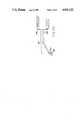
- FIGS. 3a-3dshow some embodiments of the probe pin alignment tool.
- FIGS. 3a-3cAll are variations of a shaft-like member 301 having a small loop or aperture 302 at one end 303 and a second end 304 attached to a handle 305.
- the member 301is an old probe pin, the narrow end 303 formed into the aperture 302.
- the member 301 diameteris about 2-4 mils at the loop 302, and about 10 mils at end 304.
- the aperture 302 inside diameteris about 4 mils.
- One important characteristic of the member 301 usedis that it should be at least as stiff as the probe pin to be bent.
- the userholds the handle 305 and slips the aperture 302 over the end of a probe pin to be bent.
- the inventionis then used to manually bend the probe pin.
- FIG. 3bThe presently preferred embodiment is shown in FIG. 3b. It is different from the embodiment of FIG. 3a in that the wire end 303' is hooked over the shaft 301' to prevent the aperture 302' from flexing open and breaking off.
- FIG. 3cshows wire 306" folded and twisted, the fold forming the aperture 302", and the twisted wire 306" ends attached to the handle 305".
- the aperture and handlebeing one element instead of two elements connected together; or the aperture having an angularity or notch on its inside or outside perimeter to aid in catching, forcing and bending a probe pin; a reduced or eliminated shaft; the shaft having one or more bends to help position the loop in tight spaces; the aperture being open; the aperture consisting more than one loop of wire; the aperture and shaft being made of flat stock instead of wire stock.
Landscapes
- Physics & Mathematics (AREA)
- General Physics & Mathematics (AREA)
- Engineering & Computer Science (AREA)
- Condensed Matter Physics & Semiconductors (AREA)
- Manufacturing & Machinery (AREA)
- Computer Hardware Design (AREA)
- Microelectronics & Electronic Packaging (AREA)
- Power Engineering (AREA)
- Measuring Leads Or Probes (AREA)
Abstract
Description
This invention relates to the maintenance and repair of probe pins located on probe cards such as used during the wafer-sort stage of a semiconductor manufacturing process.
In the wafer-sort stage of the manufacturing of semiconductor devices, devices are tested while still in wafer form. In this stage a critical component called a probe card is used. The probe card interfaces a tester to the semiconductor device.
The probe card, depicted in FIG. 1, typically consists of a printed circuit board with probe pins mounted in an epoxy ring, configured such that the tester can be connected to the probe card and have continuity to pads on the semiconductor device via the probe pins touching the pads. The probe pins are generally made of hard, thin, tapered wire, each bent specifically to contact just one pad without contacting neighboring pins or pads.
Because the semiconductor device under test is typically very small, the probe pins are correspondingly small and very close together. In the present application, a typical probe pin diameter might be 1.5 mils at the tip, tapered to 10 mils at the base, and a pad can be 2-4 mils wide, 1-2 mils between it and the next pad. Generally, dozens of pins are required to access all pads on a device. In order for the probe card to properly contact the pads, the tips should be positioned within a 1 mil range in planarity (vertical or z positioning, perpendicular to the card) and 0.1 mil in alignment (horizontal or x-y positioning). 1 mil planarity means that as the probe pins descend on the pads, all tips must contact the pads within 1 mil of descent from the point that a first tip contacts a pad. 0.1 mil alignment means that each probe tip must contact its pad in the center, not varying more than 0.1 mil in any direction. The scale of this can be appreciated when one realizes that a human hair is roughly 4 mils wide (see FIGS. 1 and 2).
Aligning these pins to such tolerances is challenging because they are so small and because they are generally made of a hard material such as tungsten. A probe card is mounted underneath a microscope and each pin is individually, manually worked until it comes within tolerance. This process can take hours.
Precision manipulating hand tools are not available for this work, so the technician constructs his own by bending a sharp tweezer tip into a tiny hook. The hook is then used to pull and stroke the pin this way or that, until the pin is bent to proper alignment. A disadvantage to the hook is that it does not push very well, which can make the process awkward.
The probe pin alignment tool is simply a stiff wire loop attached to a handle. The loop wire diameter is approximately the same as the diameter of the probe pin to be bent. The loop is slipped over the end of the probe pin, allowing force to be manually applied to the pin in any direction without changing the tool position.
Although bending probe pins is the application of choice, the invention can be applied to bending other sorts of wire.
FIG. 1 shows a probe pin portion of a probe card from the underside (the device under test side), actual size.
FIG. 2 details box A of FIG. 1, indicating pad positions of a device under test, also showing a side view of a probe pin.
FIGS. 3a-3d show some embodiments of the probe pin alignment tool.
Several embodiments of the invention are shown in FIGS. 3a-3c. All are variations of a shaft-like member 301 having a small loop oraperture 302 at oneend 303 and asecond end 304 attached to ahandle 305. In the original prototype (FIG. 3a) themember 301 is an old probe pin, thenarrow end 303 formed into theaperture 302. In this embodiment, themember 301 diameter is about 2-4 mils at theloop 302, and about 10 mils atend 304. Theaperture 302 inside diameter is about 4 mils. One important characteristic of themember 301 used is that it should be at least as stiff as the probe pin to be bent.
In use, the user holds thehandle 305 and slips theaperture 302 over the end of a probe pin to be bent. The invention is then used to manually bend the probe pin.
The presently preferred embodiment is shown in FIG. 3b. It is different from the embodiment of FIG. 3a in that the wire end 303' is hooked over the shaft 301' to prevent the aperture 302' from flexing open and breaking off.
An alternative embodiment is shown in FIG. 3c, which showswire 306" folded and twisted, the fold forming theaperture 302", and thetwisted wire 306" ends attached to thehandle 305".
Clearly, modifications can be made to the invention without stepping outside the claims, such as: the aperture and handle being one element instead of two elements connected together; or the aperture having an angularity or notch on its inside or outside perimeter to aid in catching, forcing and bending a probe pin; a reduced or eliminated shaft; the shaft having one or more bends to help position the loop in tight spaces; the aperture being open; the aperture consisting more than one loop of wire; the aperture and shaft being made of flat stock instead of wire stock.
Claims (2)
1. Apparatus for bending a probe pin, comprising a member attached to a handle, having a substantially closed aperture with a general diameter larger than a diameter of the probe pin, so that said aperture can be easily positioned around the probe pin, said member being made of wire at least as stiff as the probe pin and having a substantially straight shaft, a first end of said shaft being formed into at least one loop, so making said aperture, and a second end of said shaft connected to said handle, said first end being wrapped at least partially around said shaft, to prevent said aperture from flexing open, and said first end's cross-sectional area being less than said second end's cross-sectional area.
2. The apparatus of claim 1, further comprising:
said shaft having at least one bend to aid in positioning the aperture.
Priority Applications (1)
| Application Number | Priority Date | Filing Date | Title |
|---|---|---|---|
| US07/286,855US4892122A (en) | 1988-12-19 | 1988-12-19 | Probe pin alignment tool |
Applications Claiming Priority (1)
| Application Number | Priority Date | Filing Date | Title |
|---|---|---|---|
| US07/286,855US4892122A (en) | 1988-12-19 | 1988-12-19 | Probe pin alignment tool |
Publications (1)
| Publication Number | Publication Date |
|---|---|
| US4892122Atrue US4892122A (en) | 1990-01-09 |
Family
ID=23100460
Family Applications (1)
| Application Number | Title | Priority Date | Filing Date |
|---|---|---|---|
| US07/286,855Expired - LifetimeUS4892122A (en) | 1988-12-19 | 1988-12-19 | Probe pin alignment tool |
Country Status (1)
| Country | Link |
|---|---|
| US (1) | US4892122A (en) |
Cited By (10)
| Publication number | Priority date | Publication date | Assignee | Title |
|---|---|---|---|---|
| US20020053734A1 (en)* | 1993-11-16 | 2002-05-09 | Formfactor, Inc. | Probe card assembly and kit, and methods of making same |
| US6604395B2 (en)* | 2001-07-23 | 2003-08-12 | St Assembly Test Services Ltd. | Semi-automated probe bender |
| US20030199179A1 (en)* | 1993-11-16 | 2003-10-23 | Formfactor, Inc. | Contact tip structure for microelectronic interconnection elements and method of making same |
| US20040036490A1 (en)* | 2002-08-26 | 2004-02-26 | Ralph Schaeffer | Selectively configurable probe structures, e.g., for testing microelectronic components |
| US20060237856A1 (en)* | 1993-11-16 | 2006-10-26 | Formfactor, Inc. | Microelectronic Contact Structure And Method Of Making Same |
| US20070216431A1 (en)* | 2006-02-08 | 2007-09-20 | Bahadir Tunaboylu | Automated probe card planarization and alignment methods and tools |
| WO2007092592A3 (en)* | 2006-02-08 | 2007-12-21 | Sv Probe Pte Ltd | Automated probe card planarization and alignment methods and tools |
| US20090158583A1 (en)* | 2007-12-19 | 2009-06-25 | Rivera Rudel P | Head gimbal assembly (HGA) connector pad alignment jig |
| US20100093229A1 (en)* | 1996-02-21 | 2010-04-15 | Formfactor, Inc. | Microelectronic contact structure and method of making same |
| US20100117672A1 (en)* | 2008-11-13 | 2010-05-13 | Dcg Systems, Inc. | Probe tip to device pad alignment in obscured view probing applications |
Citations (11)
| Publication number | Priority date | Publication date | Assignee | Title |
|---|---|---|---|---|
| GB287773A (en)* | 1927-08-17 | 1928-03-29 | Georg Angel | Improvements in tensioning devices for fencing wire |
| US2573198A (en)* | 1950-12-18 | 1951-10-30 | Saul J Hoffman | Straightening tool for vacuum tube terminal plugs |
| US2701589A (en)* | 1952-06-14 | 1955-02-08 | Stephen P Mckinney | Loop-forming tool |
| AT181562B (en)* | 1949-01-12 | 1955-04-12 | Gerald Waterworth Cafferata | Hand tool for twisting wire ends |
| FR64749E (en)* | 1953-10-27 | 1955-12-01 | Wire tensioner | |
| AT219444B (en)* | 1958-05-24 | 1962-01-25 | Agfa Ag | Plastic containers for packaging solutions of chemical substances, in particular photographic treatment baths in concentrated form |
| US3313189A (en)* | 1965-06-15 | 1967-04-11 | Marra Lewis | Dual cartridge construction for repair product |
| GB1273289A (en)* | 1970-11-23 | 1972-05-03 | Faynot & Cie Sa | Means for stretching or straining wire |
| US3742987A (en)* | 1970-05-28 | 1973-07-03 | Hughes Aircraft Co | Pin alignment apparatus |
| US3941165A (en)* | 1975-02-13 | 1976-03-02 | Richard P. Wheat | Wire lead straightening device |
| US4510686A (en)* | 1983-04-11 | 1985-04-16 | Universal Instruments Corporation | Method and apparatus for straightening and aligning leads and testing electrical functioning of components |
- 1988
- 1988-12-19USUS07/286,855patent/US4892122A/ennot_activeExpired - Lifetime
Patent Citations (11)
| Publication number | Priority date | Publication date | Assignee | Title |
|---|---|---|---|---|
| GB287773A (en)* | 1927-08-17 | 1928-03-29 | Georg Angel | Improvements in tensioning devices for fencing wire |
| AT181562B (en)* | 1949-01-12 | 1955-04-12 | Gerald Waterworth Cafferata | Hand tool for twisting wire ends |
| US2573198A (en)* | 1950-12-18 | 1951-10-30 | Saul J Hoffman | Straightening tool for vacuum tube terminal plugs |
| US2701589A (en)* | 1952-06-14 | 1955-02-08 | Stephen P Mckinney | Loop-forming tool |
| FR64749E (en)* | 1953-10-27 | 1955-12-01 | Wire tensioner | |
| AT219444B (en)* | 1958-05-24 | 1962-01-25 | Agfa Ag | Plastic containers for packaging solutions of chemical substances, in particular photographic treatment baths in concentrated form |
| US3313189A (en)* | 1965-06-15 | 1967-04-11 | Marra Lewis | Dual cartridge construction for repair product |
| US3742987A (en)* | 1970-05-28 | 1973-07-03 | Hughes Aircraft Co | Pin alignment apparatus |
| GB1273289A (en)* | 1970-11-23 | 1972-05-03 | Faynot & Cie Sa | Means for stretching or straining wire |
| US3941165A (en)* | 1975-02-13 | 1976-03-02 | Richard P. Wheat | Wire lead straightening device |
| US4510686A (en)* | 1983-04-11 | 1985-04-16 | Universal Instruments Corporation | Method and apparatus for straightening and aligning leads and testing electrical functioning of components |
Cited By (25)
| Publication number | Priority date | Publication date | Assignee | Title |
|---|---|---|---|---|
| US20060237856A1 (en)* | 1993-11-16 | 2006-10-26 | Formfactor, Inc. | Microelectronic Contact Structure And Method Of Making Same |
| US20030199179A1 (en)* | 1993-11-16 | 2003-10-23 | Formfactor, Inc. | Contact tip structure for microelectronic interconnection elements and method of making same |
| US8373428B2 (en) | 1993-11-16 | 2013-02-12 | Formfactor, Inc. | Probe card assembly and kit, and methods of making same |
| US20020053734A1 (en)* | 1993-11-16 | 2002-05-09 | Formfactor, Inc. | Probe card assembly and kit, and methods of making same |
| US7601039B2 (en) | 1993-11-16 | 2009-10-13 | Formfactor, Inc. | Microelectronic contact structure and method of making same |
| US8033838B2 (en) | 1996-02-21 | 2011-10-11 | Formfactor, Inc. | Microelectronic contact structure |
| US20100093229A1 (en)* | 1996-02-21 | 2010-04-15 | Formfactor, Inc. | Microelectronic contact structure and method of making same |
| US6604395B2 (en)* | 2001-07-23 | 2003-08-12 | St Assembly Test Services Ltd. | Semi-automated probe bender |
| US6924653B2 (en) | 2002-08-26 | 2005-08-02 | Micron Technology, Inc. | Selectively configurable microelectronic probes |
| US20050206399A1 (en)* | 2002-08-26 | 2005-09-22 | Micron Technology, Inc. | Selectively configurable probe structures, e.g., for testing microelectronic components |
| US6972580B2 (en) | 2002-08-26 | 2005-12-06 | Micron Technology, Inc. | Selectively configurable probe structures, e.g., for testing microelectronic components |
| US6952109B2 (en) | 2002-08-26 | 2005-10-04 | Micron Technology, Inc. | Selectively configurable probe structures, e.g., for testing microelectronic components |
| US7145355B2 (en) | 2002-08-26 | 2006-12-05 | Micron Technology, Inc. | Selectively configurable probe structures, e.g., for testing microelectronic components |
| US7170304B2 (en) | 2002-08-26 | 2007-01-30 | Micron Technology, Inc. | Selectively configurable probe structures, e.g., selectively configurable probe cards for testing microelectronic components |
| US20040036490A1 (en)* | 2002-08-26 | 2004-02-26 | Ralph Schaeffer | Selectively configurable probe structures, e.g., for testing microelectronic components |
| US20050024071A1 (en)* | 2002-08-26 | 2005-02-03 | Ralph Schaeffer | Selectively configurable probe structures, e.g., for testing microelectronic components |
| US20050024072A1 (en)* | 2002-08-26 | 2005-02-03 | Ralph Schaeffer | Selectively configurable probe structures, e.g., for testing microelectronic components |
| US20050258848A1 (en)* | 2002-08-26 | 2005-11-24 | Ralph Schaeffer | Selectively configurable probe strucutres, e.g., for testing microelectronic components |
| US7583098B2 (en) | 2006-02-08 | 2009-09-01 | Sv Probe Pte. Ltd. | Automated probe card planarization and alignment methods and tools |
| WO2007092592A3 (en)* | 2006-02-08 | 2007-12-21 | Sv Probe Pte Ltd | Automated probe card planarization and alignment methods and tools |
| US20070216431A1 (en)* | 2006-02-08 | 2007-09-20 | Bahadir Tunaboylu | Automated probe card planarization and alignment methods and tools |
| US20090158583A1 (en)* | 2007-12-19 | 2009-06-25 | Rivera Rudel P | Head gimbal assembly (HGA) connector pad alignment jig |
| US8024853B2 (en) | 2007-12-19 | 2011-09-27 | Hitachi Global Storage Technologies, Netherlands B.V. | Head gimbal assembly (HGA) connector pad alignment jig |
| US20100117672A1 (en)* | 2008-11-13 | 2010-05-13 | Dcg Systems, Inc. | Probe tip to device pad alignment in obscured view probing applications |
| US8159243B2 (en) | 2008-11-13 | 2012-04-17 | Dcg Systems, Inc. | Probe tip to device pad alignment in obscured view probing applications |
Similar Documents
| Publication | Publication Date | Title |
|---|---|---|
| US5521522A (en) | Probe apparatus for testing multiple integrated circuit dies | |
| US5890390A (en) | Method and apparatus for mounting, inspecting and adjusting probe card needles | |
| US4892122A (en) | Probe pin alignment tool | |
| US5124646A (en) | Universal probe card for use in a semiconductor chip die sorter test | |
| JP3090477B2 (en) | Probe card having vertical needle and method for manufacturing probe card | |
| US4382228A (en) | Probes for fixed point probe cards | |
| KR100430208B1 (en) | Test assembly | |
| JPH02183177A (en) | Mounting device for electric test | |
| JP2003294787A (en) | Contactor, manufacturing method thereof and test method using contactor | |
| US4177425A (en) | Multiple contact electrical test probe assembly | |
| US5266895A (en) | Probe with contact portion including Au and Cu alloy | |
| US20080157797A1 (en) | Probe, probe card, and testing device | |
| US7132839B2 (en) | Ultra-short low-force vertical probe test head and method | |
| KR102283282B1 (en) | Vertical probe card with improved alignment efficiency | |
| US4847553A (en) | Needle card contacting mechanism for testing micro-electronic components | |
| EP0740160A1 (en) | Vertically operative probe card assembly | |
| US6011405A (en) | Apparatus and method for probing multiple integrated circuit dice in a semiconductor wafer | |
| US6864697B1 (en) | Flip-over alignment station for probe needle adjustment | |
| KR20030033206A (en) | Probe micro-structure | |
| JPH1019991A (en) | Test head for circuit board tester | |
| JPH11185912A (en) | Jig for semiconductor measurement | |
| KR100446551B1 (en) | Volcano type probe, its manufacturing method and probe card having it | |
| JPH04334039A (en) | Semiconductor inspecting device | |
| JPH06140482A (en) | Probe device | |
| JPH06124985A (en) | Probe equipment and probing method |
Legal Events
| Date | Code | Title | Description |
|---|---|---|---|
| AS | Assignment | Owner name:MICRON TECHNOLOGY, INC., 2805 E. COLUMBIA ROAD, BO Free format text:ASSIGNMENT OF ASSIGNORS INTEREST.;ASSIGNOR:ICKES, JOHN M.;REEL/FRAME:004986/0863 Effective date:19881212 Owner name:MICRON TECHNOLOGY, INC., A CORP. OF DE, IDAHO Free format text:ASSIGNMENT OF ASSIGNORS INTEREST;ASSIGNOR:ICKES, JOHN M.;REEL/FRAME:004986/0863 Effective date:19881212 | |
| REMI | Maintenance fee reminder mailed | ||
| FEPP | Fee payment procedure | Free format text:PETITION RELATED TO MAINTENANCE FEES FILED (ORIGINAL EVENT CODE: PMFP); ENTITY STATUS OF PATENT OWNER: LARGE ENTITY | |
| FEPP | Fee payment procedure | Free format text:PETITION RELATED TO MAINTENANCE FEES GRANTED (ORIGINAL EVENT CODE: PMFG); ENTITY STATUS OF PATENT OWNER: LARGE ENTITY | |
| REIN | Reinstatement after maintenance fee payment confirmed | ||
| FPAY | Fee payment | Year of fee payment:4 | |
| SULP | Surcharge for late payment | ||
| STCF | Information on status: patent grant | Free format text:PATENTED CASE | |
| FP | Lapsed due to failure to pay maintenance fee | Effective date:19940109 | |
| DP | Notification of acceptance of delayed payment of maintenance fee | ||
| FPAY | Fee payment | Year of fee payment:8 | |
| FPAY | Fee payment | Year of fee payment:12 |