US4891828A - Voltage to pulse-width conversion circuit - Google Patents
Voltage to pulse-width conversion circuitDownload PDFInfo
- Publication number
- US4891828A US4891828AUS07/165,716US16571688AUS4891828AUS 4891828 AUS4891828 AUS 4891828AUS 16571688 AUS16571688 AUS 16571688AUS 4891828 AUS4891828 AUS 4891828A
- Authority
- US
- United States
- Prior art keywords
- signal
- output signal
- voltage
- analog
- producing
- Prior art date
- Legal status (The legal status is an assumption and is not a legal conclusion. Google has not performed a legal analysis and makes no representation as to the accuracy of the status listed.)
- Expired - Lifetime
Links
- 238000006243chemical reactionMethods0.000titleabstractdescription29
- 230000010355oscillationEffects0.000claimsdescription25
- 238000001514detection methodMethods0.000claimsdescription15
- 230000001052transient effectEffects0.000claimsdescription2
- 239000003990capacitorSubstances0.000description7
- 238000010586diagramMethods0.000description6
- 230000000694effectsEffects0.000description3
- 238000005286illuminationMethods0.000description3
- 230000007423decreaseEffects0.000description2
- 238000000034methodMethods0.000description2
- 238000012986modificationMethods0.000description2
- 230000004048modificationEffects0.000description2
- 230000009471actionEffects0.000description1
- 238000013459approachMethods0.000description1
- 238000010420art techniqueMethods0.000description1
- 230000008859changeEffects0.000description1
- 238000010276constructionMethods0.000description1
- 230000006870functionEffects0.000description1
- 230000004313glareEffects0.000description1
- 230000010354integrationEffects0.000description1
- 238000004519manufacturing processMethods0.000description1
- 230000008569processEffects0.000description1
- 230000009467reductionEffects0.000description1
- 239000004065semiconductorSubstances0.000description1
- 238000003079width controlMethods0.000description1
Images


Classifications
- H—ELECTRICITY
- H03—ELECTRONIC CIRCUITRY
- H03K—PULSE TECHNIQUE
- H03K7/00—Modulating pulses with a continuously-variable modulating signal
- H03K7/08—Duration or width modulation ; Duty cycle modulation
- Y—GENERAL TAGGING OF NEW TECHNOLOGICAL DEVELOPMENTS; GENERAL TAGGING OF CROSS-SECTIONAL TECHNOLOGIES SPANNING OVER SEVERAL SECTIONS OF THE IPC; TECHNICAL SUBJECTS COVERED BY FORMER USPC CROSS-REFERENCE ART COLLECTIONS [XRACs] AND DIGESTS
- Y10—TECHNICAL SUBJECTS COVERED BY FORMER USPC
- Y10S—TECHNICAL SUBJECTS COVERED BY FORMER USPC CROSS-REFERENCE ART COLLECTIONS [XRACs] AND DIGESTS
- Y10S315/00—Electric lamp and discharge devices: systems
- Y10S315/04—Dimming circuit for fluorescent lamps
Definitions
- This inventionrelates to a voltage to pulse-width conversion circuit for adjusting the brightness of an electronic indicating device such as a fluorescent character display tube or the like.
- Some automobilesare provided with an electronic indicating panel on a dashboard which is controlled by a driving circuit and which may be used, for example, for an audio system, etc.
- a voltage to pulse-width conversion circuithas been used to control the pulse-width of a drive signal from the driving circuit to the segment electrode of an indicating panel for adjusting the brightness of the indicating panel.
- FIG. 2shows one of conventional analog type voltage to pulse-width conversion circuits which comprises a voltage comparator 20 having a positive input for receiving a pulse width control signal S1 through an input terminal 1 and an output 2 for producing a pulse width modulation signal (hereinafter referred to as a PWM signal) S2, and a CR oscillation circuit 10.
- a CR oscillation circuit 10has an output terminal connected to the negative input of voltage comparator 20. An output of the voltage comparator 20 is connected to the output terminal 2.
- the CR oscillation circuit 10produces sawtooth waveform signals S10.
- This circuitconsists of a voltage comparator 11 having an NPN transistor in a collector open state, a capacitor 12, and five resistors 13-17.
- the voltage comparators 11 and 20operate on the positive voltage V10 of a current source used for an electronic indicator device (not shown in the figure).
- a signal S11a divided by the resistors 13 and 14is applied to the positive input of the voltage comparator 11.
- the voltage comparator 11has a negative input for receiving a signal S11b which is supplied through resistor 17.
- the input terminal 1is connected to an input circuit which supplies a PWM input signal S1.
- This input circuithas a switch 30 for illumination of the interior of an automobile during a night drive.
- the switch 30has one terminal connected to a positive voltage V30 of a 13.8 V battery and the other terminal connected to a variable resistor 31 which is normally adjusted by a driver.
- the variable resistor 31supplies a divided voltage across the resistors 32 and 33, an intermediate node between the registers 32 and 33 is connected to the input terminal 1.
- FIG. 3shows signal waveforms generated in the circuit of FIG. 2.
- FIG. 4is a chart which illustrates input-output characteristics of the circuit of FIG. 2. Operation of the circuit of FIG. 2 will now be described with reference to FIGS. 3 and 4.
- the CR oscillation circuit 10begins to oscillate and normally generates on its output an oscillation signal S10 having a frequency of about 128 Hz.
- This signal S10is fed to the negative of voltage comparator 20.
- the frequency and waveform of oscillation signal S10are determined by the time constant of the capacitor 12 and the resistors 13-17. More specifically, when capacitor 12 is charged through the resistors, the potential of an input signal S11b on the negative input of comparator 11 is increased. At this moment, the potential of input signal S11a entering the positive-input of voltage comparator 11 also is slightly increased under the effect of a feed back resistor 15 based on a reference potential divided by resistors 13 and 14.
- a feed back resistor 17has a much lower value of resistance than those of the other resistors 13-16.
- the input signal S11aalso quickly decreases its potential. The amount of such a change in the potential is determined by values of the resistors 13 to 17.
- the voltage comparator 11When the potential of the input signal S11b falls below that of the input signal S11a, the voltage comparator 11 is set OFF, and until the potential of the input signal S11b becomes higher than that of the input signal S11a, the capacitor 12 will be charged through the resistors. Such an action will sustain operation of the CR oscillation circuit 10.
- the battery voltage V30is supplied across the variable resistor 31.
- a voltage divided by the variable resistor 31is subdivided by the voltage dividing resistors 32 and 33.
- the voltage at the point between resistors 32 and 33is fed to the input terminal 1 in the form of a PWM input signal S1 supplied to the positive input of the voltage comparator 20.
- the level of the PWM input signal S1varies as shown in FIG. 3 as S1-1 and S1-2.
- the voltage comparator 20compares the level of the output signal S10 with that of the PWM input signal S1, performs a voltage to pulse-width conversion, and supplies a PWM output signal S2 to the output terminal 2.
- the PWM output signal S2first falls into a high level (hereinafter designated merely by the letter "H”) at a range of S10 ⁇ S1 and then becomes "L" at a range of S10 > S1.
- the input-output characteristics of PWM output signal S2 versus PWM input signal S1 as shown in FIG. 4are determined by the output waveform of the CR oscillation circuit 10.
- FIG. 5illustrates an example of a conventional digital type voltage to pulse-width conversion circuit.
- This voltage to pulse-width conversion circuithas an analog/digital converter (hereinafter referred to as an A/D converter).
- the circuithas an input terminal 40 for receiving a PWM input signal S1, an input terminal 41 for receiving a reference frequency signal S0, and an output terminal 42 for generating a PWM output signal S2.
- Installed in series between the input terminal 40 and the output terminal 42are a ten-bit A/D converter 43, a (1024 word x ten-bit) read-only memory (hereinafter referred to as ROM) 44, and a ten-bit PWM generation circuit 45.
- the input terminal 41is also connected to an input of a timing generation circuit 46.
- An output of the circuit 46is connected to the A/D converter 43, the ROM 44, and the PWM generation circuit 45.
- the timing generation circuit 46When a reference frequency signal S0 is supplied to the input terminal 40, the timing generation circuit 46 generates a timing signal to be supplied to the A/D converter 43, the ROM 44, and the PWM generation circuit 45.
- the A/D converter 43converts the PWM input signal S1 into a digital signal to be transmitted to the ROM 44.
- the ROM 44reads out the data corresponding to the digital signal, and the PWM generation circuit 45 generates a PWM output signal S2 corresponding to the received data to the output terminal 42.
- each of the resistors 13-17requires a very high resistance value i.e., of about several hundred kOhm. Therefore, it is very difficult to integrate the CR oscillation circuit 10 in a semiconductor IC chip.
- the variations in resistance values of the resistors 13-17 due to process conditionsaffect the output oscillation waveform and decrease the frequency stability of the PWM output signal S2.
- the use of external resistors 13-17increases the number of IC lead terminals. It will not be practical to make a voltage to pulse-width conversion circuit by using discrete components, because there is generally not enough mounting space on the back side of the indicating panel of a car radio (tuner).
- An object of this inventionis to provide a voltage to pulse-width conversion circuit which solves the problems associated with the prior art technique and makes it possible to minimize the actual dimensions of the IC chip.
- D/A converterdigital/analog converter
- a countercounts a reference frequency signal and sends the counted number signal to a D/A converter.
- the D/A converterconverts the digital value obtained into an analog signal which, in turn, is transmitted to a comparator.
- the comparatorcompares the analog signal with the PWM input signal in levels and outputs the PWM output signal having a duty ratio.
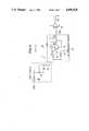
- FIG. 1is a circuit diagram of a voltage to pulse width conversion circuit according to the first embodiment of this invention.
- FIG. 2is a circuit diagram of a conventional analog type voltage to pulse-width conversion circuit.
- FIG. 3shows waveforms of signals generated by the circuit of FIG. 2.
- FIG. 4shows input-output characteristics of the circuit of FIG. 2.
- FIG. 5is a conventional digital type voltage to pulse-width conversion circuit.
- FIG. 6is a circuit diagram of D/A converter used in the circuit of FIG. 1.
- FIG. 7shows waveforms of signals generated by the circuit of FIGS. 1 and 6.
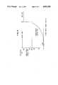
- FIG. 8shows input-output characteristics of the circuit of FIG. 1.
- FIG. 9is a circuit diagram of a voltage to pulse-width conversion circuit in accordance with the second embodiment of this invention.
- FIG. 1A voltage to pulse-width conversion circuit in accordance with the first embodiment of this invention is shown in FIG. 1.
- the voltage to pulse-width conversion circuit shown in this figurecomprises an oscillation circuit which incorporates a multi-bit counter 54 and a multi-bit D/A converter 55.
- This oscillation circuitcorresponds to the CR oscillation circuit 10 of the conventional circuit shown in FIG. 2.
- the voltage to pulse-width conversion circuit of this inventionhas an input terminal 50 for receiving a PWM input signal S50, an input terminal 51 for receiving a reference frequency signal S51, and an output terminal 52 which issues a PWM output signal S52, e.g., of 128 Hz.
- the input terminal 50is connected to a positive input of a voltage comparator 53, whereas an output of comparator 53 is connected to output terminal 52.
- Input terminal 51is also connected to a counter 54, e.g., an eight-bit binary counter.
- An output terminal of counter 54is connected to an input terminal 55a of, e.g., a six-bit D/A converter 55.
- the D/A converter 55converts the output signal of the counter 54, which is fed to input terminal 55a, into an analog signal.
- This analog signal S55is generated on an output terminal 55b, which is connected to a negative input of voltage comparator 53.
- the input terminal 50is connected to an input circuit for suppling PWM input signal S50.
- the input circuithas a switch 60 which illuminates various meters on a dashboard in an automobile during a night drive.
- One terminal of switch 60receives a positive battery voltage V60 (which is normally 13.8 V), while the other terminal thereof is grounded through a variable resistor 61 which is manually adjusted.
- An output terminal of the variable resistor 61is grounded through the voltage-dividing resistors 62 and 63. The point of interconnection between the voltage-dividing resistors 62 and 63 is connected to the input terminal 50.
- the input terminal 51is connected to an oscillator 64 which supplies a reference frequency signal S51, e.g., of 32.768 KHz.
- the other terminal of switch 60is also connected to an input of a detection circuit 65 which detects an OFF condition of the switch 60 and produces a high level signal, or ⁇ H ⁇ level signal.
- An output terminal of the detection circuit 65is connected to an input terminal of a logical OR gate 66 which has two inputs and an output for providing a PWM output signal S66 to a driving circuit.
- FIG. 6is a circuit diagram of the six-bit D/A converter 55 of FIG. 1.
- the D/A converter 55comprises a resistance, voltage-dividing type converter which has a decoder 70, analog switches 71-1 to 71-64, and voltage-dividing resistors 72-1 to 72-64.
- the decoder 70includes an input terminal 55a for receiving eight-bit signals 2 o to 2 7 , and OUT 0-1, OUT2 to OUT63, and OUT64-255 output terminals.
- the decoder 70decodes the input signals and produces decoded signals on its output.
- Each output terminal (i.e., OUT0-1, OUT2 to OUT63, OUT64-255) of decoder 70is connected to a respective control input terminal of an analog switch 71-1 to 71-64.
- each analog switch 71-1 to 71-64is connected to an output terminal 55b, while the other side of each analog switch 71-1 to 71-64 is connected to a point between respective voltage-dividing resistors 72-1 to 72-64.
- the one side of analog switch 71-1 and one side of the voltage-dividing resistor 72-1are grounded, and the other sides of the analog switch 71-64 and the voltage-dividing resistor 72-64 are connected to a reference voltage V o .
- the output terminal OUT0-1 of the decoder 70issues a signal S70-1, and the output terminal OUT64-255 issues the signal S70-2.
- FIG. 7shows signal waveforms seen in the circuits in FIGS. 1 and 6.
- FIG. 8illustrates input-output characteristics of the circuit of FIG. 1. The operation of circuits of FIGS. 1 and 6 will now be explained with reference to FIGS. 7 and 8.
- the circuit of FIG. 1will be energized, the oscillator 64 begins to oscillate and produces on its output a reference signal S51 of 32.768 kHz.
- This signal S51is supplied through the input terminal 51 to the eight-bit counter 54 which continuously counts from 0 to 255.
- the counter 54feeds the output to the input terminal 55a of the six-bit D/A converter 55.
- the decoder 70successively selects one of the output terminals OUT0-1, OUT2 to OUT63, OUT64-255, in accordance with a counted value to switch successively ON a selected one of the analog switches 71-1 to 71-64 via selected output terminals OUT0-1, OUT2 to OUT63, OUT64-255, and then to output a voltage signal S55 divided by resistors 72-1 to 72-64 to the output terminal 55b.
- the decoder 70when the counter 54 counts a value of 0 or 1, the decoder 70 set only the analog switch 71-1 to an ON state to provide OV signal S55 to the output terminal 55b.
- the decoder 70sets only the analog switch 71-2 to an ON state to a fraction voltage between the resistors 72-1 and 72-2 as a signal S22 to the output terminal 55b.
- the decoder 70selects the analog switches 71-1 to 71-64 to supply the signal S55 having waveforms as seen in FIG. 7 to the negative input of the voltage comparator 53.
- the linear curve between counted values 2 and 63is represented in a staircase form in detail.
- variable resistor 61When the indicator illumination switch 60 is ON for driving an automobile at night, a 13.8 V battery voltage v60 is supplied across the variable resistor 61 which can produce a divided voltage signal between 0 and 13.8 V.
- the divided voltageis applied to the resistance voltage-divider.
- the resistance values of the resistors 62 and 63are determined on the swing range of an output signal S55 of the D/A converter 55, as well as on the swing range of an input signal of the voltage comparator 53.
- the divided voltage of the resistance voltage-divideris fed to the positive input terminal of the voltage comparator 53 as a PWM input signal S50 through input terminal 50.
- the level of the PWM input signal S50can be varied by means of variable resistor 61, as shown in FIG. 7 as signals S50-1 and S50-2.
- the voltage comparator 53compares the output signal S55 of D/A converter 55 with the PWM input signal S50 to output a PWM output signal S52 to the terminal 52.
- the PWM output signal S52becomes "H” within the range of S50 ⁇ S55, and "L” within the range of S50 ⁇ S55. Therefore, as shown in FIG. 7, the PWM output signal S52 having a duty ratio corresponding to the voltage of PWM input signals S50 can be obtained by adjusting the variable resistor 61.
- the PWM control range for night drivingcorresponds to the duty ratio of PWM output signal S52 between 1 and 25%.
- the characteristic curve of PWM output signal S52 in the 1%-25% zoneis not linear and fine adjustments can be performed in the vicinity of 1% duty ratio while coarse adjustments can be performed near the 25% duty ratio.
- a drivercan freely adjust the PWM control ranges.
- the waveform of output signal S55 of the converter 55determines such PWM characteristics.
- the desired waveform of output signal S55can be obtained by changing a resistance ratio between the resistors 72-1 to 72-64.
- the PWM controlwhich has fine adjustment characteristics near 1% duty ratio and coarse adjustment characteristics near 25% duty ratio can be obtained by upwardly and gradually reducing the resistors 72-2 to 72-63 in resistance value.
- the use of the D/A converter 55 shown in FIG. 6has the following advantages. If the reference voltage V o is stable, the level stability of the output signal S55 is determined by a resistance ratio among the voltage-dividing resistors 72-1 to 72-64. Therefore, integrated voltage dividing resistors are sufficiently practical, if resistance deviation of e.g., below 2%, is guaranteed by controlling IC manufacturing tolerances. This means that the output signal S55 is required to have linear characteristics only over a setting range.
- Setting of the circuit for day or night-time drivingis performed by switching the switch 60 ON or OFF. For example, when the switch 60 is ON, night time mode is detected and when the switch 60 is OFF, and the day-time mode is detected. When the switch 60 is ON, the detection circuit 65 outputs an "H" level signal whereby the OR gate 66 provides the PWM output signal S66 of a 100% duty ratio in day-time mode.
- FIG. 9shows a circuit diagram of a voltage to pulse-width conversion circuit in accordance with the second embodiment of the present invention.
- the elements identical with those shown in FIG. 1are designated by the same reference numerals.
- the voltage to pulse-width conversion circuithas an additional circuit 80 connected between one input terminal of the OR gate 66 and the output terminal 52, and oscillator 64 having a terminal for receiving a control signal from the detection circuit 65 to stop the oscillation.
- an eight-bit counter 54is provided with a reset terminal R for receiving a control signal from the detection circuit 65 to perform a reset function.
- the additional circuit 80consists of a D-type flip-flop (hereinafter referred to as D-FF) 81 and a two-input OR gate 82.
- the OR gate 82can positively maintain the 1% duty ratio of the PWM characteristic as shown FIG. 8, even though PWM input signal approaches zero.
- One input terminal of this OR gate 82is connected to the output terminal 52, while the other input terminal of the OR gate 82 is connected to the output terminal OUT0-1 of decoder 70 in D/A converter 55.
- the D-FF circuitprevents unfavorable effects to the PWM output signal due to a transient spike or overshoot (glitch) which occurs in the ON/OFF operation of the analog switches 71-1 to 71-64.
- the D-FF 81its data input terminal D is connected to an output terminal of OR gate 82, its clock terminal is connected to an output terminal of oscillator 64, while its output terminal Q is connected to an input terminal of OR gate 66.
- the counter 54may be a different bit counter and may be a counter having a different coding system. In that case, the decoder 70 of D/A converter 55 should be naturally matched with the corresponding counting code.
- the six-bit resistor-type voltage-dividing D/A converter 55may be replaced by other types and other bit-number D/A converters.
- the voltage to pulse-width conversion circuit of this inventioncomprises a counter, a D/A converter, and a voltage comparator, it is small in size and it has a reduced number of terminals as well a reduced number of externally components. This makes easily possible a single chip integration with a drive circuit for a display device as well as cost reduction of the device.
- the conversion circuitcan be easily mounted into the limited space for an electronic display device of an automobile, etc.
- the characteristics of a PWM output signal versus a PWM input signalcan be arbitrarily selected at the design stage. As a result, the brightness control can be conducted with high accuracy.
- An input offset voltage below 5 mVdoes not affect the accuracy of the comparator. Since the accuracy of the resistor-type voltage-dividing D/A converter depends on the resistance ratio of several voltage-dividing resistors, the conversion accuracy due to temperature variations is improved over that of a conventional analog type converter.
- the conversion circuit of this inventionmay find wide practical applications in brightness control circuits for car audio devices (such as tuners, cassette decks, compact discs, car clocks, or similar information indicator devices), or for other electronic indicator devices.
- car audio devicessuch as tuners, cassette decks, compact discs, car clocks, or similar information indicator devices
Landscapes
- Analogue/Digital Conversion (AREA)
- Arrangements Of Lighting Devices For Vehicle Interiors, Mounting And Supporting Thereof, Circuits Therefore (AREA)
Abstract
Description
Claims (11)
Applications Claiming Priority (2)
| Application Number | Priority Date | Filing Date | Title |
|---|---|---|---|
| JP62-53386 | 1987-03-09 | ||
| JP62053386AJP2698580B2 (en) | 1987-03-09 | 1987-03-09 | Voltage / pulse width conversion circuit |
Publications (1)
| Publication Number | Publication Date |
|---|---|
| US4891828Atrue US4891828A (en) | 1990-01-02 |
Family
ID=12941386
Family Applications (1)
| Application Number | Title | Priority Date | Filing Date |
|---|---|---|---|
| US07/165,716Expired - LifetimeUS4891828A (en) | 1987-03-09 | 1988-03-08 | Voltage to pulse-width conversion circuit |
Country Status (2)
| Country | Link |
|---|---|
| US (1) | US4891828A (en) |
| JP (1) | JP2698580B2 (en) |
Cited By (46)
| Publication number | Priority date | Publication date | Assignee | Title |
|---|---|---|---|---|
| US5105127A (en)* | 1989-06-30 | 1992-04-14 | Thomson-Csf | Dimming method and device for fluorescent lamps used for backlighting of liquid crystal screens |
| US5192922A (en)* | 1992-05-29 | 1993-03-09 | Analog Devices, Inc. | Anti-false triggering system for a pulse width modulation system |
| US5198785A (en)* | 1992-05-29 | 1993-03-30 | Analog Devices, Inc. | Dual edge pulse width modulation system |
| US5208559A (en)* | 1992-05-29 | 1993-05-04 | Analog Devices, Inc. | Pulse shaping system for a pulse width modulation system |
| US5277497A (en)* | 1991-03-04 | 1994-01-11 | Oki Electric Industry Co., Ltd. | Voltage to pulse-width conversion circuit |
| EP0545077A3 (en)* | 1991-12-06 | 1994-04-27 | Bosch Gmbh Robert | |
| US5321315A (en)* | 1992-03-09 | 1994-06-14 | Eastman Kodak Company | Tracking control pulse generation for variable frame rate CCD sensors for electronic imaging applications |
| US5339009A (en)* | 1991-08-08 | 1994-08-16 | Ford Motor Company | Method and apparatus for distinguishing input signals and generating a common dimming signal |
| US5481214A (en)* | 1993-07-22 | 1996-01-02 | Oki Electric Industry Co., Ltd. | Voltage to pulse-width conversion circuit |
| US5894239A (en)* | 1997-04-18 | 1999-04-13 | International Business Machines Corporation | Single shot with pulse width controlled by reference oscillator |
| US5936564A (en)* | 1996-07-09 | 1999-08-10 | Samsung Electronics Co., Ltd. | Digital to analog converter using pulse width modulation and the controlling method thereof |
| US6531834B2 (en)* | 2000-09-28 | 2003-03-11 | Patent-Treuhand-Gesellschaft Fuer Elektrische Gluehlampen Mbh | Circuit arrangement for controlling an analog voltage signal |
| US6570347B2 (en) | 2000-06-01 | 2003-05-27 | Everbrite, Inc. | Gas-discharge lamp having brightness control |
| US20090015736A1 (en)* | 2005-11-01 | 2009-01-15 | Donnelly Corporation | Interior rearview mirror assembly with display |
| US20090219394A1 (en)* | 1998-01-07 | 2009-09-03 | Donnelly Corporation | Accessory mounting system suitable for use in a vehicle |
| US20090316422A1 (en)* | 2001-01-23 | 2009-12-24 | Donnelly Corporation | Display device for exterior rearview mirror |
| US20100033797A1 (en)* | 2003-10-02 | 2010-02-11 | Donnelly Corporation | Mirror reflective element assembly |
| US7821697B2 (en) | 1994-05-05 | 2010-10-26 | Donnelly Corporation | Exterior reflective mirror element for a vehicular rearview mirror assembly |
| US7859737B2 (en) | 2002-09-20 | 2010-12-28 | Donnelly Corporation | Interior rearview mirror system for a vehicle |
| US7864399B2 (en) | 2002-09-20 | 2011-01-04 | Donnelly Corporation | Reflective mirror assembly |
| US7871169B2 (en) | 1994-05-05 | 2011-01-18 | Donnelly Corporation | Vehicular signal mirror |
| US20110026152A1 (en)* | 2002-06-06 | 2011-02-03 | Donnelly Corporation | Interior rearview mirror system |
| US20110035120A1 (en)* | 2000-03-02 | 2011-02-10 | Donnelly Corporation | Vehicular wireless communication system |
| US7898398B2 (en) | 1997-08-25 | 2011-03-01 | Donnelly Corporation | Interior mirror system |
| US7906756B2 (en) | 2002-05-03 | 2011-03-15 | Donnelly Corporation | Vehicle rearview mirror system |
| US7916009B2 (en) | 1998-01-07 | 2011-03-29 | Donnelly Corporation | Accessory mounting system suitable for use in a vehicle |
| US7914188B2 (en) | 1997-08-25 | 2011-03-29 | Donnelly Corporation | Interior rearview mirror system for a vehicle |
| US7918570B2 (en) | 2002-06-06 | 2011-04-05 | Donnelly Corporation | Vehicular interior rearview information mirror system |
| US7926960B2 (en) | 1999-11-24 | 2011-04-19 | Donnelly Corporation | Interior rearview mirror system for vehicle |
| US20110109746A1 (en)* | 2003-10-14 | 2011-05-12 | Donnelly Corporation | Vehicle information display |
| US20110166785A1 (en)* | 1998-04-08 | 2011-07-07 | Donnelly Corporation | Interior rearview mirror system |
| US8044776B2 (en) | 2000-03-02 | 2011-10-25 | Donnelly Corporation | Rear vision system for vehicle |
| US8049640B2 (en) | 2003-05-19 | 2011-11-01 | Donnelly Corporation | Mirror assembly for vehicle |
| US8072318B2 (en) | 2001-01-23 | 2011-12-06 | Donnelly Corporation | Video mirror system for vehicle |
| US8154418B2 (en) | 2008-03-31 | 2012-04-10 | Magna Mirrors Of America, Inc. | Interior rearview mirror system |
| US8194133B2 (en) | 2000-03-02 | 2012-06-05 | Donnelly Corporation | Vehicular video mirror system |
| US8277059B2 (en) | 2002-09-20 | 2012-10-02 | Donnelly Corporation | Vehicular electrochromic interior rearview mirror assembly |
| US8288711B2 (en) | 1998-01-07 | 2012-10-16 | Donnelly Corporation | Interior rearview mirror system with forwardly-viewing camera and a control |
| US8294975B2 (en) | 1997-08-25 | 2012-10-23 | Donnelly Corporation | Automotive rearview mirror assembly |
| US8462204B2 (en) | 1995-05-22 | 2013-06-11 | Donnelly Corporation | Vehicular vision system |
| US8503062B2 (en) | 2005-05-16 | 2013-08-06 | Donnelly Corporation | Rearview mirror element assembly for vehicle |
| US9019091B2 (en) | 1999-11-24 | 2015-04-28 | Donnelly Corporation | Interior rearview mirror system |
| CN106535412A (en)* | 2016-12-21 | 2017-03-22 | 贵州恒芯微电子科技有限公司 | Digital-analogue dimming circuit with shared port |
| CN113765464A (en)* | 2020-05-28 | 2021-12-07 | 广东美的暖通设备有限公司 | Voltage conversion device, motor control system and air conditioner |
| TWI760766B (en)* | 2020-06-11 | 2022-04-11 | 瑞鼎科技股份有限公司 | Pulse-width modulation detection circuit and method for power saving and anti-noise |
| EP4398484A3 (en)* | 2022-12-13 | 2024-10-30 | LX Semicon Co., Ltd. | Pulse width modulation signal generation circuit and lamp control system including the same |
Citations (10)
| Publication number | Priority date | Publication date | Assignee | Title |
|---|---|---|---|---|
| US3906247A (en)* | 1974-01-16 | 1975-09-16 | Gte Automatic Electric Lab Inc | Programmable proportional clock edge delay circuit |
| US4028609A (en)* | 1975-12-22 | 1977-06-07 | Westinghouse Electric Corporation | Digital firing pulse generator with pulse suppression |
| US4241295A (en)* | 1979-02-21 | 1980-12-23 | Williams Walter E Jr | Digital lighting control system |
| US4287468A (en)* | 1978-08-28 | 1981-09-01 | Robert Sherman | Dimmer control system |
| US4330751A (en)* | 1979-12-03 | 1982-05-18 | Norlin Industries, Inc. | Programmable frequency and duty cycle tone signal generator |
| US4365202A (en)* | 1980-08-25 | 1982-12-21 | Rca Corporation | Duty cycle generator with improved resolution |
| US4370067A (en)* | 1978-04-11 | 1983-01-25 | Citizen Watch Company Limited | Electronic timepiece with gain/loss adjustment |
| US4396869A (en)* | 1979-03-05 | 1983-08-02 | Leviton Manufacturing Company, Inc. | Time responsive variable voltage power supply |
| US4415861A (en)* | 1981-06-08 | 1983-11-15 | Tektronix, Inc. | Programmable pulse generator |
| US4754163A (en)* | 1983-07-08 | 1988-06-28 | Hewlett-Packard Company | Pulse generator with adjustable pulse frequency, pulse width and pulse delay |
Family Cites Families (1)
| Publication number | Priority date | Publication date | Assignee | Title |
|---|---|---|---|---|
| JPS5821852A (en)* | 1981-08-03 | 1983-02-08 | Semiconductor Energy Lab Co Ltd | Semiconductor device |
- 1987
- 1987-03-09JPJP62053386Apatent/JP2698580B2/ennot_activeExpired - Lifetime
- 1988
- 1988-03-08USUS07/165,716patent/US4891828A/ennot_activeExpired - Lifetime
Patent Citations (10)
| Publication number | Priority date | Publication date | Assignee | Title |
|---|---|---|---|---|
| US3906247A (en)* | 1974-01-16 | 1975-09-16 | Gte Automatic Electric Lab Inc | Programmable proportional clock edge delay circuit |
| US4028609A (en)* | 1975-12-22 | 1977-06-07 | Westinghouse Electric Corporation | Digital firing pulse generator with pulse suppression |
| US4370067A (en)* | 1978-04-11 | 1983-01-25 | Citizen Watch Company Limited | Electronic timepiece with gain/loss adjustment |
| US4287468A (en)* | 1978-08-28 | 1981-09-01 | Robert Sherman | Dimmer control system |
| US4241295A (en)* | 1979-02-21 | 1980-12-23 | Williams Walter E Jr | Digital lighting control system |
| US4396869A (en)* | 1979-03-05 | 1983-08-02 | Leviton Manufacturing Company, Inc. | Time responsive variable voltage power supply |
| US4330751A (en)* | 1979-12-03 | 1982-05-18 | Norlin Industries, Inc. | Programmable frequency and duty cycle tone signal generator |
| US4365202A (en)* | 1980-08-25 | 1982-12-21 | Rca Corporation | Duty cycle generator with improved resolution |
| US4415861A (en)* | 1981-06-08 | 1983-11-15 | Tektronix, Inc. | Programmable pulse generator |
| US4754163A (en)* | 1983-07-08 | 1988-06-28 | Hewlett-Packard Company | Pulse generator with adjustable pulse frequency, pulse width and pulse delay |
Cited By (156)
| Publication number | Priority date | Publication date | Assignee | Title |
|---|---|---|---|---|
| US5105127A (en)* | 1989-06-30 | 1992-04-14 | Thomson-Csf | Dimming method and device for fluorescent lamps used for backlighting of liquid crystal screens |
| US5277497A (en)* | 1991-03-04 | 1994-01-11 | Oki Electric Industry Co., Ltd. | Voltage to pulse-width conversion circuit |
| US5339009A (en)* | 1991-08-08 | 1994-08-16 | Ford Motor Company | Method and apparatus for distinguishing input signals and generating a common dimming signal |
| EP0545077A3 (en)* | 1991-12-06 | 1994-04-27 | Bosch Gmbh Robert | |
| US5321315A (en)* | 1992-03-09 | 1994-06-14 | Eastman Kodak Company | Tracking control pulse generation for variable frame rate CCD sensors for electronic imaging applications |
| US5192922A (en)* | 1992-05-29 | 1993-03-09 | Analog Devices, Inc. | Anti-false triggering system for a pulse width modulation system |
| US5198785A (en)* | 1992-05-29 | 1993-03-30 | Analog Devices, Inc. | Dual edge pulse width modulation system |
| US5208559A (en)* | 1992-05-29 | 1993-05-04 | Analog Devices, Inc. | Pulse shaping system for a pulse width modulation system |
| WO1993025000A1 (en)* | 1992-05-29 | 1993-12-09 | Analog Devices, Inc. | Pulse shaping system for a pulse width modulation system |
| WO1993024999A1 (en)* | 1992-05-29 | 1993-12-09 | Analog Devices, Inc. | Dual edge pulse width modulation system |
| WO1993025001A1 (en)* | 1992-05-29 | 1993-12-09 | Analog Devices, Inc. | Anti-false triggering system for a pulse width modulation system |
| US5481214A (en)* | 1993-07-22 | 1996-01-02 | Oki Electric Industry Co., Ltd. | Voltage to pulse-width conversion circuit |
| US7821697B2 (en) | 1994-05-05 | 2010-10-26 | Donnelly Corporation | Exterior reflective mirror element for a vehicular rearview mirror assembly |
| US8511841B2 (en) | 1994-05-05 | 2013-08-20 | Donnelly Corporation | Vehicular blind spot indicator mirror |
| US7871169B2 (en) | 1994-05-05 | 2011-01-18 | Donnelly Corporation | Vehicular signal mirror |
| US8164817B2 (en) | 1994-05-05 | 2012-04-24 | Donnelly Corporation | Method of forming a mirrored bent cut glass shape for vehicular exterior rearview mirror assembly |
| US8559093B2 (en) | 1995-04-27 | 2013-10-15 | Donnelly Corporation | Electrochromic mirror reflective element for vehicular rearview mirror assembly |
| US8462204B2 (en) | 1995-05-22 | 2013-06-11 | Donnelly Corporation | Vehicular vision system |
| US5936564A (en)* | 1996-07-09 | 1999-08-10 | Samsung Electronics Co., Ltd. | Digital to analog converter using pulse width modulation and the controlling method thereof |
| US5894239A (en)* | 1997-04-18 | 1999-04-13 | International Business Machines Corporation | Single shot with pulse width controlled by reference oscillator |
| US8779910B2 (en) | 1997-08-25 | 2014-07-15 | Donnelly Corporation | Interior rearview mirror system |
| US8610992B2 (en) | 1997-08-25 | 2013-12-17 | Donnelly Corporation | Variable transmission window |
| US8063753B2 (en) | 1997-08-25 | 2011-11-22 | Donnelly Corporation | Interior rearview mirror system |
| US8294975B2 (en) | 1997-08-25 | 2012-10-23 | Donnelly Corporation | Automotive rearview mirror assembly |
| US8100568B2 (en) | 1997-08-25 | 2012-01-24 | Donnelly Corporation | Interior rearview mirror system for a vehicle |
| US8309907B2 (en) | 1997-08-25 | 2012-11-13 | Donnelly Corporation | Accessory system suitable for use in a vehicle and accommodating a rain sensor |
| US20110140606A1 (en)* | 1997-08-25 | 2011-06-16 | Donnelly Corporation | Interior rearview mirror system |
| US8267559B2 (en) | 1997-08-25 | 2012-09-18 | Donnelly Corporation | Interior rearview mirror assembly for a vehicle |
| US7898398B2 (en) | 1997-08-25 | 2011-03-01 | Donnelly Corporation | Interior mirror system |
| US7914188B2 (en) | 1997-08-25 | 2011-03-29 | Donnelly Corporation | Interior rearview mirror system for a vehicle |
| US7888629B2 (en) | 1998-01-07 | 2011-02-15 | Donnelly Corporation | Vehicular accessory mounting system with a forwardly-viewing camera |
| US7916009B2 (en) | 1998-01-07 | 2011-03-29 | Donnelly Corporation | Accessory mounting system suitable for use in a vehicle |
| US8325028B2 (en) | 1998-01-07 | 2012-12-04 | Donnelly Corporation | Interior rearview mirror system |
| US8288711B2 (en) | 1998-01-07 | 2012-10-16 | Donnelly Corporation | Interior rearview mirror system with forwardly-viewing camera and a control |
| US20090219394A1 (en)* | 1998-01-07 | 2009-09-03 | Donnelly Corporation | Accessory mounting system suitable for use in a vehicle |
| US8134117B2 (en) | 1998-01-07 | 2012-03-13 | Donnelly Corporation | Vehicular having a camera, a rain sensor and a single-ball interior electrochromic mirror assembly attached at an attachment element |
| US7994471B2 (en) | 1998-01-07 | 2011-08-09 | Donnelly Corporation | Interior rearview mirror system with forwardly-viewing camera |
| US8094002B2 (en) | 1998-01-07 | 2012-01-10 | Donnelly Corporation | Interior rearview mirror system |
| US8525703B2 (en) | 1998-04-08 | 2013-09-03 | Donnelly Corporation | Interior rearview mirror system |
| US8884788B2 (en) | 1998-04-08 | 2014-11-11 | Donnelly Corporation | Automotive communication system |
| US9221399B2 (en) | 1998-04-08 | 2015-12-29 | Magna Mirrors Of America, Inc. | Automotive communication system |
| US20110166785A1 (en)* | 1998-04-08 | 2011-07-07 | Donnelly Corporation | Interior rearview mirror system |
| US9481306B2 (en) | 1998-04-08 | 2016-11-01 | Donnelly Corporation | Automotive communication system |
| US9376061B2 (en) | 1999-11-24 | 2016-06-28 | Donnelly Corporation | Accessory system of a vehicle |
| US10144355B2 (en) | 1999-11-24 | 2018-12-04 | Donnelly Corporation | Interior rearview mirror system for vehicle |
| US7926960B2 (en) | 1999-11-24 | 2011-04-19 | Donnelly Corporation | Interior rearview mirror system for vehicle |
| US9019091B2 (en) | 1999-11-24 | 2015-04-28 | Donnelly Corporation | Interior rearview mirror system |
| US9278654B2 (en) | 1999-11-24 | 2016-03-08 | Donnelly Corporation | Interior rearview mirror system for vehicle |
| US8162493B2 (en) | 1999-11-24 | 2012-04-24 | Donnelly Corporation | Interior rearview mirror assembly for vehicle |
| US20110176323A1 (en)* | 1999-11-24 | 2011-07-21 | Donnelly Corporation | Interior rearview mirror assembly for vehicle |
| US10131280B2 (en) | 2000-03-02 | 2018-11-20 | Donnelly Corporation | Vehicular video mirror system |
| US9019090B2 (en) | 2000-03-02 | 2015-04-28 | Magna Electronics Inc. | Vision system for vehicle |
| US8095310B2 (en) | 2000-03-02 | 2012-01-10 | Donnelly Corporation | Video mirror system for a vehicle |
| US20110035120A1 (en)* | 2000-03-02 | 2011-02-10 | Donnelly Corporation | Vehicular wireless communication system |
| US10053013B2 (en) | 2000-03-02 | 2018-08-21 | Magna Electronics Inc. | Vision system for vehicle |
| US8121787B2 (en) | 2000-03-02 | 2012-02-21 | Donnelly Corporation | Vehicular video mirror system |
| US8427288B2 (en) | 2000-03-02 | 2013-04-23 | Donnelly Corporation | Rear vision system for a vehicle |
| US9809168B2 (en) | 2000-03-02 | 2017-11-07 | Magna Electronics Inc. | Driver assist system for vehicle |
| US9809171B2 (en) | 2000-03-02 | 2017-11-07 | Magna Electronics Inc. | Vision system for vehicle |
| US8543330B2 (en) | 2000-03-02 | 2013-09-24 | Donnelly Corporation | Driver assist system for vehicle |
| US9783114B2 (en) | 2000-03-02 | 2017-10-10 | Donnelly Corporation | Vehicular video mirror system |
| US8676491B2 (en) | 2000-03-02 | 2014-03-18 | Magna Electronics Inc. | Driver assist system for vehicle |
| US8179236B2 (en) | 2000-03-02 | 2012-05-15 | Donnelly Corporation | Video mirror system suitable for use in a vehicle |
| US8908039B2 (en) | 2000-03-02 | 2014-12-09 | Donnelly Corporation | Vehicular video mirror system |
| US8194133B2 (en) | 2000-03-02 | 2012-06-05 | Donnelly Corporation | Vehicular video mirror system |
| US9014966B2 (en) | 2000-03-02 | 2015-04-21 | Magna Electronics Inc. | Driver assist system for vehicle |
| US8044776B2 (en) | 2000-03-02 | 2011-10-25 | Donnelly Corporation | Rear vision system for vehicle |
| US8271187B2 (en) | 2000-03-02 | 2012-09-18 | Donnelly Corporation | Vehicular video mirror system |
| US9315151B2 (en) | 2000-03-02 | 2016-04-19 | Magna Electronics Inc. | Driver assist system for vehicle |
| US10179545B2 (en) | 2000-03-02 | 2019-01-15 | Magna Electronics Inc. | Park-aid system for vehicle |
| US10239457B2 (en) | 2000-03-02 | 2019-03-26 | Magna Electronics Inc. | Vehicular vision system |
| US8000894B2 (en) | 2000-03-02 | 2011-08-16 | Donnelly Corporation | Vehicular wireless communication system |
| US6570347B2 (en) | 2000-06-01 | 2003-05-27 | Everbrite, Inc. | Gas-discharge lamp having brightness control |
| US6531834B2 (en)* | 2000-09-28 | 2003-03-11 | Patent-Treuhand-Gesellschaft Fuer Elektrische Gluehlampen Mbh | Circuit arrangement for controlling an analog voltage signal |
| US10272839B2 (en) | 2001-01-23 | 2019-04-30 | Magna Electronics Inc. | Rear seat occupant monitoring system for vehicle |
| US9352623B2 (en) | 2001-01-23 | 2016-05-31 | Magna Electronics Inc. | Trailer hitching aid system for vehicle |
| US20090316422A1 (en)* | 2001-01-23 | 2009-12-24 | Donnelly Corporation | Display device for exterior rearview mirror |
| US9694749B2 (en) | 2001-01-23 | 2017-07-04 | Magna Electronics Inc. | Trailer hitching aid system for vehicle |
| US8653959B2 (en) | 2001-01-23 | 2014-02-18 | Donnelly Corporation | Video mirror system for a vehicle |
| US8654433B2 (en) | 2001-01-23 | 2014-02-18 | Magna Mirrors Of America, Inc. | Rearview mirror assembly for vehicle |
| US8072318B2 (en) | 2001-01-23 | 2011-12-06 | Donnelly Corporation | Video mirror system for vehicle |
| US8083386B2 (en) | 2001-01-23 | 2011-12-27 | Donnelly Corporation | Interior rearview mirror assembly with display device |
| US8304711B2 (en) | 2002-05-03 | 2012-11-06 | Donnelly Corporation | Vehicle rearview mirror system |
| US8106347B2 (en) | 2002-05-03 | 2012-01-31 | Donnelly Corporation | Vehicle rearview mirror system |
| US7906756B2 (en) | 2002-05-03 | 2011-03-15 | Donnelly Corporation | Vehicle rearview mirror system |
| US8608327B2 (en) | 2002-06-06 | 2013-12-17 | Donnelly Corporation | Automatic compass system for vehicle |
| US8465163B2 (en) | 2002-06-06 | 2013-06-18 | Donnelly Corporation | Interior rearview mirror system |
| US8047667B2 (en) | 2002-06-06 | 2011-11-01 | Donnelly Corporation | Vehicular interior rearview mirror system |
| US20110181727A1 (en)* | 2002-06-06 | 2011-07-28 | Donnelly Corporation | Vehicular interior rearview mirror system |
| US8465162B2 (en) | 2002-06-06 | 2013-06-18 | Donnelly Corporation | Vehicular interior rearview mirror system |
| US20110026152A1 (en)* | 2002-06-06 | 2011-02-03 | Donnelly Corporation | Interior rearview mirror system |
| US8177376B2 (en) | 2002-06-06 | 2012-05-15 | Donnelly Corporation | Vehicular interior rearview mirror system |
| US8282226B2 (en) | 2002-06-06 | 2012-10-09 | Donnelly Corporation | Interior rearview mirror system |
| US7918570B2 (en) | 2002-06-06 | 2011-04-05 | Donnelly Corporation | Vehicular interior rearview information mirror system |
| US9545883B2 (en) | 2002-09-20 | 2017-01-17 | Donnelly Corporation | Exterior rearview mirror assembly |
| US8228588B2 (en) | 2002-09-20 | 2012-07-24 | Donnelly Corporation | Interior rearview mirror information display system for a vehicle |
| US9878670B2 (en) | 2002-09-20 | 2018-01-30 | Donnelly Corporation | Variable reflectance mirror reflective element for exterior mirror assembly |
| US10029616B2 (en) | 2002-09-20 | 2018-07-24 | Donnelly Corporation | Rearview mirror assembly for vehicle |
| US8335032B2 (en) | 2002-09-20 | 2012-12-18 | Donnelly Corporation | Reflective mirror assembly |
| US8506096B2 (en) | 2002-09-20 | 2013-08-13 | Donnelly Corporation | Variable reflectance mirror reflective element for exterior mirror assembly |
| US8727547B2 (en) | 2002-09-20 | 2014-05-20 | Donnelly Corporation | Variable reflectance mirror reflective element for exterior mirror assembly |
| US7864399B2 (en) | 2002-09-20 | 2011-01-04 | Donnelly Corporation | Reflective mirror assembly |
| US8797627B2 (en) | 2002-09-20 | 2014-08-05 | Donnelly Corporation | Exterior rearview mirror assembly |
| US10363875B2 (en) | 2002-09-20 | 2019-07-30 | Donnelly Corportion | Vehicular exterior electrically variable reflectance mirror reflective element assembly |
| US9341914B2 (en) | 2002-09-20 | 2016-05-17 | Donnelly Corporation | Variable reflectance mirror reflective element for exterior mirror assembly |
| US8277059B2 (en) | 2002-09-20 | 2012-10-02 | Donnelly Corporation | Vehicular electrochromic interior rearview mirror assembly |
| US10661716B2 (en) | 2002-09-20 | 2020-05-26 | Donnelly Corporation | Vehicular exterior electrically variable reflectance mirror reflective element assembly |
| US7859737B2 (en) | 2002-09-20 | 2010-12-28 | Donnelly Corporation | Interior rearview mirror system for a vehicle |
| US8400704B2 (en) | 2002-09-20 | 2013-03-19 | Donnelly Corporation | Interior rearview mirror system for a vehicle |
| US10538202B2 (en) | 2002-09-20 | 2020-01-21 | Donnelly Corporation | Method of manufacturing variable reflectance mirror reflective element for exterior mirror assembly |
| US9073491B2 (en) | 2002-09-20 | 2015-07-07 | Donnelly Corporation | Exterior rearview mirror assembly |
| US9090211B2 (en) | 2002-09-20 | 2015-07-28 | Donnelly Corporation | Variable reflectance mirror reflective element for exterior mirror assembly |
| US10829052B2 (en) | 2003-05-19 | 2020-11-10 | Donnelly Corporation | Rearview mirror assembly for vehicle |
| US10166927B2 (en) | 2003-05-19 | 2019-01-01 | Donnelly Corporation | Rearview mirror assembly for vehicle |
| US8325055B2 (en) | 2003-05-19 | 2012-12-04 | Donnelly Corporation | Mirror assembly for vehicle |
| US9783115B2 (en) | 2003-05-19 | 2017-10-10 | Donnelly Corporation | Rearview mirror assembly for vehicle |
| US8049640B2 (en) | 2003-05-19 | 2011-11-01 | Donnelly Corporation | Mirror assembly for vehicle |
| US11433816B2 (en) | 2003-05-19 | 2022-09-06 | Magna Mirrors Of America, Inc. | Vehicular interior rearview mirror assembly with cap portion |
| US8508384B2 (en) | 2003-05-19 | 2013-08-13 | Donnelly Corporation | Rearview mirror assembly for vehicle |
| US10449903B2 (en) | 2003-05-19 | 2019-10-22 | Donnelly Corporation | Rearview mirror assembly for vehicle |
| US9557584B2 (en) | 2003-05-19 | 2017-01-31 | Donnelly Corporation | Rearview mirror assembly for vehicle |
| US8705161B2 (en) | 2003-10-02 | 2014-04-22 | Donnelly Corporation | Method of manufacturing a reflective element for a vehicular rearview mirror assembly |
| US8179586B2 (en) | 2003-10-02 | 2012-05-15 | Donnelly Corporation | Rearview mirror assembly for vehicle |
| US20100033797A1 (en)* | 2003-10-02 | 2010-02-11 | Donnelly Corporation | Mirror reflective element assembly |
| US20110141542A1 (en)* | 2003-10-02 | 2011-06-16 | Donnelly Corporation | Rearview mirror assembly for vehicle |
| US7898719B2 (en) | 2003-10-02 | 2011-03-01 | Donnelly Corporation | Rearview mirror assembly for vehicle |
| US8379289B2 (en) | 2003-10-02 | 2013-02-19 | Donnelly Corporation | Rearview mirror assembly for vehicle |
| US8170748B1 (en) | 2003-10-14 | 2012-05-01 | Donnelly Corporation | Vehicle information display system |
| US8019505B2 (en) | 2003-10-14 | 2011-09-13 | Donnelly Corporation | Vehicle information display |
| US8355839B2 (en) | 2003-10-14 | 2013-01-15 | Donnelly Corporation | Vehicle vision system with night vision function |
| US8577549B2 (en) | 2003-10-14 | 2013-11-05 | Donnelly Corporation | Information display system for a vehicle |
| US20110109746A1 (en)* | 2003-10-14 | 2011-05-12 | Donnelly Corporation | Vehicle information display |
| US8095260B1 (en) | 2003-10-14 | 2012-01-10 | Donnelly Corporation | Vehicle information display |
| US8282253B2 (en) | 2004-11-22 | 2012-10-09 | Donnelly Corporation | Mirror reflective element sub-assembly for exterior rearview mirror of a vehicle |
| US8503062B2 (en) | 2005-05-16 | 2013-08-06 | Donnelly Corporation | Rearview mirror element assembly for vehicle |
| US10150417B2 (en) | 2005-09-14 | 2018-12-11 | Magna Mirrors Of America, Inc. | Mirror reflective element sub-assembly for exterior rearview mirror of a vehicle |
| US10829053B2 (en) | 2005-09-14 | 2020-11-10 | Magna Mirrors Of America, Inc. | Vehicular exterior rearview mirror assembly with blind spot indicator |
| US11285879B2 (en) | 2005-09-14 | 2022-03-29 | Magna Mirrors Of America, Inc. | Vehicular exterior rearview mirror assembly with blind spot indicator element |
| US11072288B2 (en) | 2005-09-14 | 2021-07-27 | Magna Mirrors Of America, Inc. | Vehicular exterior rearview mirror assembly with blind spot indicator element |
| US8833987B2 (en) | 2005-09-14 | 2014-09-16 | Donnelly Corporation | Mirror reflective element sub-assembly for exterior rearview mirror of a vehicle |
| US9694753B2 (en) | 2005-09-14 | 2017-07-04 | Magna Mirrors Of America, Inc. | Mirror reflective element sub-assembly for exterior rearview mirror of a vehicle |
| US10308186B2 (en) | 2005-09-14 | 2019-06-04 | Magna Mirrors Of America, Inc. | Vehicular exterior rearview mirror assembly with blind spot indicator |
| US9758102B1 (en) | 2005-09-14 | 2017-09-12 | Magna Mirrors Of America, Inc. | Mirror reflective element sub-assembly for exterior rearview mirror of a vehicle |
| US9045091B2 (en) | 2005-09-14 | 2015-06-02 | Donnelly Corporation | Mirror reflective element sub-assembly for exterior rearview mirror of a vehicle |
| US20090015736A1 (en)* | 2005-11-01 | 2009-01-15 | Donnelly Corporation | Interior rearview mirror assembly with display |
| US11124121B2 (en) | 2005-11-01 | 2021-09-21 | Magna Electronics Inc. | Vehicular vision system |
| US7855755B2 (en) | 2005-11-01 | 2010-12-21 | Donnelly Corporation | Interior rearview mirror assembly with display |
| US11970113B2 (en) | 2005-11-01 | 2024-04-30 | Magna Electronics Inc. | Vehicular vision system |
| US8508383B2 (en) | 2008-03-31 | 2013-08-13 | Magna Mirrors of America, Inc | Interior rearview mirror system |
| US8154418B2 (en) | 2008-03-31 | 2012-04-10 | Magna Mirrors Of America, Inc. | Interior rearview mirror system |
| US10175477B2 (en) | 2008-03-31 | 2019-01-08 | Magna Mirrors Of America, Inc. | Display system for vehicle |
| CN106535412B (en)* | 2016-12-21 | 2018-07-10 | 贵州恒芯微电子科技有限公司 | The digital simulation light adjusting circuit that a kind of port shares |
| CN106535412A (en)* | 2016-12-21 | 2017-03-22 | 贵州恒芯微电子科技有限公司 | Digital-analogue dimming circuit with shared port |
| CN113765464A (en)* | 2020-05-28 | 2021-12-07 | 广东美的暖通设备有限公司 | Voltage conversion device, motor control system and air conditioner |
| TWI760766B (en)* | 2020-06-11 | 2022-04-11 | 瑞鼎科技股份有限公司 | Pulse-width modulation detection circuit and method for power saving and anti-noise |
| EP4398484A3 (en)* | 2022-12-13 | 2024-10-30 | LX Semicon Co., Ltd. | Pulse width modulation signal generation circuit and lamp control system including the same |
Also Published As
| Publication number | Publication date |
|---|---|
| JPS63219222A (en) | 1988-09-12 |
| JP2698580B2 (en) | 1998-01-19 |
Similar Documents
| Publication | Publication Date | Title |
|---|---|---|
| US4891828A (en) | Voltage to pulse-width conversion circuit | |
| US9257964B2 (en) | Low frequency oscillator for burst-mode dimming control for CCFL driver system | |
| US7372312B2 (en) | Pulse width modulation generating circuit | |
| US4588934A (en) | Automobile fan control with non-periodic fluctuation signal generator | |
| US4241294A (en) | Brightness control circuit for a vacuum fluorescent display | |
| GB2079498A (en) | A power circuit for an electronic timepiece | |
| CN110445483B (en) | PWM signal generation and error correction circuit thereof | |
| JP3053658B2 (en) | Voltage / pulse width modulation circuit | |
| US5583605A (en) | Photoelectric current converting circuit | |
| CN113437954B (en) | Jitter frequency adjusting circuit, jitter frequency adjusting method and chip | |
| US4114100A (en) | Rapid tuning circuit for high frequency receivers | |
| EP0753839B1 (en) | Selective-calling radio receiver capable of vibration warning | |
| US4365236A (en) | Digital display circuit displayable in analog fashion | |
| US7154310B2 (en) | Trapezoid signal generating circuit | |
| US5481214A (en) | Voltage to pulse-width conversion circuit | |
| US7123179B1 (en) | Apparatus and method for duty cycle conversion | |
| JP3026412B2 (en) | Voltage / pulse width conversion circuit | |
| EP0602929A1 (en) | Sync signal detection apparatus | |
| US5283476A (en) | Waveform generator | |
| CN210518241U (en) | PWM signal generation and error correction circuit thereof | |
| US20020135575A1 (en) | Liquid crystal driving power supply | |
| EP0167865B1 (en) | Driving circuit for liquid crystal display | |
| CN114204922B (en) | Modulation circuit and modulation method for pulse width modulation signal | |
| KR0139663B1 (en) | Frequency auto regulational voltage controlled oscillator | |
| CN111884548B (en) | Motor driving circuit and driving method based on capacitor charging and discharging structure |
Legal Events
| Date | Code | Title | Description |
|---|---|---|---|
| AS | Assignment | Owner name:OKI ELECTRIC INDUSTRY CO., LTD., 7-12, TORANOMON 1 Free format text:ASSIGNMENT OF ASSIGNORS INTEREST.;ASSIGNOR:KAWAZOE, AKIO;REEL/FRAME:004872/0571 Effective date:19880111 Owner name:OKI ELECTRIC INDUSTRY CO., LTD.,JAPAN Free format text:ASSIGNMENT OF ASSIGNORS INTEREST;ASSIGNOR:KAWAZOE, AKIO;REEL/FRAME:004872/0571 Effective date:19880111 | |
| STCF | Information on status: patent grant | Free format text:PATENTED CASE | |
| FEPP | Fee payment procedure | Free format text:PAYOR NUMBER ASSIGNED (ORIGINAL EVENT CODE: ASPN); ENTITY STATUS OF PATENT OWNER: LARGE ENTITY | |
| FPAY | Fee payment | Year of fee payment:4 | |
| FEPP | Fee payment procedure | Free format text:PAYER NUMBER DE-ASSIGNED (ORIGINAL EVENT CODE: RMPN); ENTITY STATUS OF PATENT OWNER: LARGE ENTITY Free format text:PAYOR NUMBER ASSIGNED (ORIGINAL EVENT CODE: ASPN); ENTITY STATUS OF PATENT OWNER: LARGE ENTITY | |
| FPAY | Fee payment | Year of fee payment:8 | |
| FPAY | Fee payment | Year of fee payment:12 |